Embed Size (px)
Citation preview

Smart Mesh
(HN-BN02) Data Sheet
BLE4.1 Module
Document No: HN-BN02-M-DS-001
Issue No: 1.3
Issue Date: 2017-04-25
A-903, Woorim W-City, 9-22, Pangyo-ro 255, Bundang-gu,
Seongnam-si, Gyeonggi-do, Republic of Korea
TEL. 82-31-609-0703 FAX. 82-2-6499-0977
E-mail. [email protected]
Smart Mesh (HN-BN02) Data Sheet
RESTRICTED DOC No: HN-BN02-M-DS-001 Issue No: 1.3 Issue Date: 2017-04-25
2 / 33
Contents
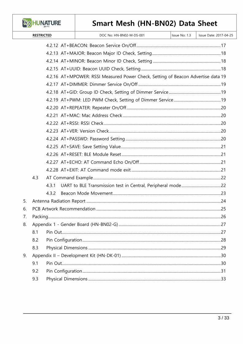
Contents ........................................................................................................................................................................................ 2
1. Introduction ........................................................................................................................................................................ 4
1.1 Related Documents ........................................................................................................................................... 4
1.2 Main Chip Features ........................................................................................................................................... 5
1.3 Application ............................................................................................................................................................ 5
2. Module Specification ...................................................................................................................................................... 6
2.1 Module Architecture ......................................................................................................................................... 6
2.2 Electrical Specification ..................................................................................................................................... 7
2.2.1 Key Specification ................................................................................................................................. 7
2.2.2 Absolute Maximum Rating ............................................................................................................. 8
2.2.3 Recommended Operating Conditions ....................................................................................... 8
2.2.4 Current Consumption ........................................................................................................................ 8
2.3 Module information .......................................................................................................................................... 9
2.3.1 Block Diagram ...................................................................................................................................... 9
2.3.2 Pin Out ..................................................................................................................................................... 9
2.3.3 Pin Configuration .............................................................................................................................. 10
2.4 Physical Dimensions ....................................................................................................................................... 11
3. Smart Mesh Network ................................................................................................................................................... 12
4. AT Command ................................................................................................................................................................... 14
4.1 Communication Environment ..................................................................................................................... 14
4.2 AT Command Set ............................................................................................................................................. 14
4.2.1 +++: Change to AT Command Mode ................................................................................... 14
4.2.2 AT+ROLE: Central, Peripheral Check, Setting ....................................................................... 14
4.2.3 AT+UART: UART Baud rate Check, Setting ........................................................................... 15
4.2.4 AT+TXPOWER: TX Power Level Check, Setting ................................................................... 15
4.2.5 AT+BIND: Mac Address Check and Setting for Target Device to Binding ............. 15
4.2.6 AT+CMODE: Connection Mode Check, Setting .................................................................. 16
4.2.7 AT+NAME: Device Name Check, Setting ............................................................................... 16
4.2.8 AT+SERIAL: Serial Number Check, Setting ............................................................................ 16
4.2.9 AT+MINCINT: Minimum Connection Interval Check, Setting ....................................... 17
4.2.10 AT+MAXCINT: Maximum Connection Interval Check, Setting ..................................... 17
4.2.11 AT+ADVINT: Beacon advertise Interval Check, Setting ................................................... 17
Smart Mesh (HN-BN02) Data Sheet
RESTRICTED DOC No: HN-BN02-M-DS-001 Issue No: 1.3 Issue Date: 2017-04-25
3 / 33
4.2.12 AT+BEACON: Beacon Service On/Off ...................................................................................... 17
4.2.13 AT+MAJOR: Beacon Major ID Check, Setting ...................................................................... 18
4.2.14 AT+MINOR: Beacon Minor ID Check, Setting ..................................................................... 18
4.2.15 AT+UUID: Beacon UUID Check, Setting ................................................................................. 18
4.2.16 AT+MPOWER: RSSI Measured Power Check, Setting of Beacon Advertise data 19
4.2.17 AT+DIMMER: Dimmer Service On/Off .................................................................................... 19
4.2.18 AT+GID: Group ID Check, Setting of Dimmer Service ..................................................... 19
4.2.19 AT+PWM: LED PWM Check, Setting of Dimmer Service ................................................ 19
4.2.20 AT+REPEATER: Repeater On/Off ................................................................................................ 20
4.2.21 AT+MAC: Mac Address Check .................................................................................................... 20
4.2.22 AT+RSSI: RSSI Check ....................................................................................................................... 20
4.2.23 AT+VER: Version Check .................................................................................................................. 20
4.2.24 AT+PASSWD: Password Setting ................................................................................................. 20
4.2.25 AT+SAVE: Save Setting Value...................................................................................................... 21
4.2.26 AT+RESET: BLE Module Reset ..................................................................................................... 21
4.2.27 AT+ECHO: AT Command Echo On/Off ................................................................................... 21
4.2.28 AT+EXIT: AT Command mode exit ........................................................................................... 21
4.3 AT Command Example .................................................................................................................................. 22
4.3.1 UART to BLE Transmission test in Central, Peripheral mode ........................................ 22
4.3.2 Beacon Mode Movement .............................................................................................................. 23
5. Antenna Radiation Report ......................................................................................................................................... 24
6. PCB Artwork Recommendation ............................................................................................................................... 25
7. Packing ................................................................................................................................................................................ 26
8. Appendix 1 - Gender Board (HN-BN02-G) ........................................................................................................ 27
8.1 Pin Out.................................................................................................................................................................. 27
8.2 Pin Configuration ............................................................................................................................................. 28
8.3 Physical Dimensions ....................................................................................................................................... 29
9. Appendix II – Development Kit (HN-DK-01) ..................................................................................................... 30
9.1 Pin Out.................................................................................................................................................................. 30
9.2 Pin Configuration ............................................................................................................................................. 31
9.3 Physical Dimensions ....................................................................................................................................... 33

Smart Mesh (HN-BN02) Data Sheet
RESTRICTED DOC No: HN-BN02-M-DS-001 Issue No: 1.3 Issue Date: 2017-04-25
4 / 33
1. Introduction
The Smart Mesh BLE (HN-BN) is a module for Bluetooth Low Energy
communication (BLE 4.1). This module enables up to 20 Byte
Segmentation, and provides Mesh network implementation function.
It also provides AT command about Beacon & setting of several BLE functions for user
convenience. Various networks can be formed as shown in Picture 1-1, using these functions.
We offers a service for building LED Dimming Network only using AT Command.
Picture 1-1 Network Topology
(a) P2P, (b) Star, (c) Mesh
It supplies Programming function through SWD Interface for SW developers. We also offer
Development Kit with which you can develop various sensors and Interface very easily.
Antenna and RF (Radio Frequency) characteristics of the Smart Mesh BLE Module are optimized,
therefore over 30-meter signal transmission is possible, and BLE network construction using
Repeater & Mesh Function is also possible. This results in greater scalability and cost reduction
of network implementation.
1.1 Related Documents
The following documents and Apps are available at www.Hunature.net .
BLE AT Command user Manual (T.B.D)
BLE Application Guide (T.B.D)
BLE Application SW for Mobile (T.B.D)

Smart Mesh (HN-BN02) Data Sheet
RESTRICTED DOC No: HN-BN02-M-DS-001 Issue No: 1.3 Issue Date: 2017-04-25
5 / 33
1.2 Main Chip Features
Single chip, highly flexible, 2.4 GHz multi-protocol device
32-bit ARM Cortex M0 CPU core
256kB flash + 32kB RAM
Supports Bluetooth low energy protocol stacks
Thread safe and run-time protected
Event driven API
On air compatible with nRF24L series
3 data rates (2Mbps/1Mbps/250kbps)
+4dBm output power
-93dBm sensitivity, Bluetooth low energy
PPI system for maximum power-efficient applications and code simplification
Flexible power management system with automatic power management of each
peripheral
Configurable I/O mapping for analog and digital I/O
Operating temperature range: -40°C to +105°C
1.3 Application
Mobile phone accessories
Wearables
Beacons
Device/System monitoring
PC peripherals
Consumer Electronics (CE) remote controls
Proximity/Alert sensors
Smart Home
Sports, fitness and healthcare sensors
Smart RF tags
Toys and electronic games
Lighting, Dimming
Repeater & Mesh Network
Sensor Network

Smart Mesh (HN-BN02) Data Sheet
RESTRICTED DOC No: HN-BN02-M-DS-001 Issue No: 1.3 Issue Date: 2017-04-25
6 / 33
2. Module Specification
2.1 Module Architecture
The Architecture of the Smart Mesh Module is shown in the following Picture 2-1.
Picture 2-1 Module Architecture

Smart Mesh (HN-BN02) Data Sheet
RESTRICTED DOC No: HN-BN02-M-DS-001 Issue No: 1.3 Issue Date: 2017-04-25
7 / 33
2.2 Electrical Specification
2.2.1 Key Specification
The Key Specification of HN-BN Bluetooth Low Energy Module is shown in Table 2.2-1 below.
Table 2.2-1 Key Specification
Item Description 비고
Main Chipset
SoC ARM Cortex-M0 32bit nRF51822 series
32kB RAM
256kB Flash
Bluetooth
Bluetooth Low Energy 4.1 stack for HN-BN02
On-module integrated chip antenna
No external trimming is required in production
RF
On-module integrated chip antenna
-93dBm sensitivity
Integrated channel filters
Clock External 16MHz, Internal 32KHz RTC
Operating Mode Running, Idle, Deep sleep
I/F SPI, I2C, UART, GPIO(Analog, Digital)
Download I/F SPI Programming (SWDIO, SWDCLK)
Network P2P, Repeater, Star, Mesh
Max 20 Byte Segmentation
AT Command Beacon (iBeacon)
LED Dimming (Dimmer)
P2P, Repeater, Star, Mesh configuration
FW Option AT Command, On Demand, Empty,

Smart Mesh (HN-BN02) Data Sheet
RESTRICTED DOC No: HN-BN02-M-DS-001 Issue No: 1.3 Issue Date: 2017-04-25
8 / 33
2.2.2 Absolute Maximum Rating
The Behavior Characteristics are displayed in Table 2.2-2.
Table 2.2-2 Absolute Maximum Rating
Operating Conditions Min Typ Max Unit
Storage temperature -40 - 85 ℃
Power Supply Voltage 1.8 - 4.4 V
2.2.3 Recommended Operating Conditions
The Behavior Characteristics are displayed in Table 2.2-3.
Table 2.2-3 Recommended Operating Conditions
Operating Conditions Min Typ Max Unit
Operating temperature -30 - 85 ℃
Power Supply Voltage 1.8 3.3 3.6 V
2.2.4 Current Consumption
The amount of current consumption is shown in Table 2.2-4.
Table 2.2-4 Current Consumption
Mode Description
Total Typical
Current at
3.0V
Deep
sleep
VDD_PADS = ON, REFCLK = OFF, SLEEPCLK = ON,
VDD_BAT = ON, RAM = ON, digital circuits = ON, SMPS =
ON (low-power mode), 2.2ms wake-up time
<5μA
Idle
VDD_PADS = ON, REFCLK = ON, SLEEPCLK = ON,
VDD_BAT = ON, RAM = ON, digital circuits = ON, MCU =
IDLE, <1μs wake-up time
~1mA
RX
active -
~ 20mA @ 3V
peak current
TX
active -
~ 18mA @ 3V
peak current

Smart Mesh (HN-BN02) Data Sheet
RESTRICTED DOC No: HN-BN02-M-DS-001 Issue No: 1.3 Issue Date: 2017-04-25
9 / 33
2.3 Module information
2.3.1 Block Diagram
The Block Diagram of BLE Block is as below Picture 2-2.
Bluetooth Low Energy Radio
Chip Antenna
MCUCortex M0 32bit
RAM32KByte
Flash 256KByte
ClockInternal 32KHz RTC
16MHz Crystal I2C/SPI
I/O
UART
PWM
Analog
Digital
RF Filter
Picture 2-2 Block Diagram
2.3.2 Pin Out
The pin configuration of the BLE block is shown in Picture 2-3 below
Picture 2-3 Pin out Diagram
Smart Mesh (HN-BN02) Data Sheet
RESTRICTED DOC No: HN-BN02-M-DS-001 Issue No: 1.3 Issue Date: 2017-04-25
10 / 33
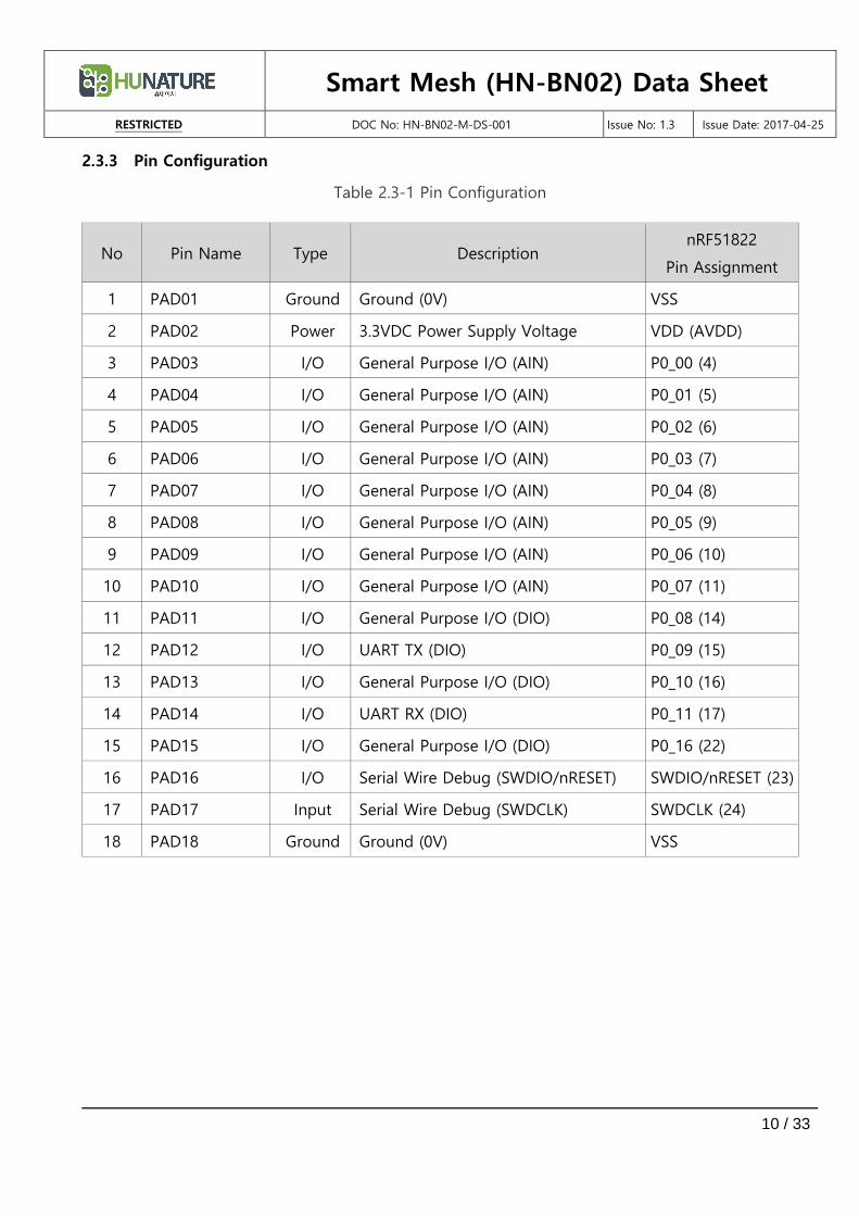
2.3.3 Pin Configuration
Table 2.3-1 Pin Configuration
No Pin Name Type Description nRF51822
Pin Assignment
1 PAD01 Ground Ground (0V) VSS
2 PAD02 Power 3.3VDC Power Supply Voltage VDD (AVDD)
3 PAD03 I/O General Purpose I/O (AIN) P0_00 (4)
4 PAD04 I/O General Purpose I/O (AIN) P0_01 (5)
5 PAD05 I/O General Purpose I/O (AIN) P0_02 (6)
6 PAD06 I/O General Purpose I/O (AIN) P0_03 (7)
7 PAD07 I/O General Purpose I/O (AIN) P0_04 (8)
8 PAD08 I/O General Purpose I/O (AIN) P0_05 (9)
9 PAD09 I/O General Purpose I/O (AIN) P0_06 (10)
10 PAD10 I/O General Purpose I/O (AIN) P0_07 (11)
11 PAD11 I/O General Purpose I/O (DIO) P0_08 (14)
12 PAD12 I/O UART TX (DIO) P0_09 (15)
13 PAD13 I/O General Purpose I/O (DIO) P0_10 (16)
14 PAD14 I/O UART RX (DIO) P0_11 (17)
15 PAD15 I/O General Purpose I/O (DIO) P0_16 (22)
16 PAD16 I/O Serial Wire Debug (SWDIO/nRESET) SWDIO/nRESET (23)
17 PAD17 Input Serial Wire Debug (SWDCLK) SWDCLK (24)
18 PAD18 Ground Ground (0V) VSS

Smart Mesh (HN-BN02) Data Sheet
RESTRICTED DOC No: HN-BN02-M-DS-001 Issue No: 1.3 Issue Date: 2017-04-25
11 / 33
2.4 Physical Dimensions
The Dimension information of BLE Module is as Picture 2-4, 2-5 below.
Picture 2-4 Dimension – Top View
Picture 2-5 Dimension – Side View

Smart Mesh (HN-BN02) Data Sheet
RESTRICTED DOC No: HN-BN02-M-DS-001 Issue No: 1.3 Issue Date: 2017-04-25
12 / 33
3. Smart Mesh Network
HN-BN supports two types of Mesh Network. Picture 3-1 illustrates the Smart Mesh Network 1
using Advertising Packet of Bluetooth, and Picture 3-3 shows the Smart Mesh Network 2, which
has the Connection Function between devices together with the function of Picture 3-1.
Picture 3-1 displays the Mesh Network constructed using Advertising Packet of HN-BN, the
data transmissions for two paths, A -> B, C -> A are marked by the orange and purple arrows
respectively. As Mesh Network is constructed, each device will broadcast the received Advertising
Packet as it is (Picture 3-1). Therefore, it is possible to improve the limited coverage of BLE like a
dotted line shown in Picture 3-2.
Picture 3-1 Smart Mesh Network 1 (Broadcasting type)
Picture 3-2 Coverage of Mesh Network

Smart Mesh (HN-BN02) Data Sheet
RESTRICTED DOC No: HN-BN02-M-DS-001 Issue No: 1.3 Issue Date: 2017-04-25
13 / 33
The Broadcasting Type Mesh Network has a very simple network configuration, but it is not a
direct exchange of information via connection between devices. If the number of devices in the
Mesh Network is very large, the quality of communication can degrade due to repetitive
Advertising of data and the increase in data traffic caused by the data propagation of the Relay
node received.
Therefore, HN-BN supports Smart Mesh Network 2 to prevent this increase in data traffic.
Picture 3-3 is a Concept Diagram of Smart Mesh Network 2 for reduction of data traffic, and this
supports the connection mode linked to C – R – D as well as the function in Picture 3-1 at the
same time.
As described in Picture 3-3, the data between C and D will be transferred directly by the
Connection, rather than by exchanging information by Broadcasting.
Picture 3-3 Smart Mesh Network 2 (Broadcasting + Connection type)
The network construction by Smart Mesh Network 2 reduces unnecessary wireless data traffic, and
enables the improvement of Coverage and communication quality by connecting more devices
than Smart Mesh Network 1.
Smart Mesh (HN-BN02) Data Sheet
RESTRICTED DOC No: HN-BN02-M-DS-001 Issue No: 1.3 Issue Date: 2017-04-25
14 / 33
4. AT Command
4.1 Communication Environment
Data Transmission: BLE Modem <-> Smart Phone App, Serial Terminal Program
Data Communication System: UART (8bit data, none parity, 1 bit stop, none flow control)
Communication Speed: 115200bps(default), can be set by AT Command
4.2 AT Command Set
<CR+LF> means Carriage-Return(0x0D) and Line-Feed(0x0A)
In UART to BLE transmission, the data received from UART are divided into 20 byte unit
and are sent to BLE. For example, when 50 bytes are received by UART, the data is divided
into 20/20/10 bytes each and send to BLE. The UART Receiving buffer consists of a FIFO
structure of 256 bytes.
The setting values for the module are available in AT Command Mode (enter " +++ "),
and the UART to BLE transmission is available in Transmit Mode (" AT + EXIT "). It
operates in Transmit Mode at boot time
4.2.1 +++: Change to AT Command Mode
AT Command Response Parameter
+++ <CR+LF>OK<CR+LF>
4.2.2 AT+ROLE: Central, Peripheral Check, Setting
AT Command Response Parameter
AT+ROLE=?<CR+LF> <CR+LF>
+ROLE=<Param>
<CR+LF>OK<CR+LF>
Param :
“C” : central
“P” : Peripheral
AT+ROLE=<Param><CR+LF> <CR+LF>OK<CR+LF>
or
<CR+LF>ERROR<CR+LF>
Param :
“C” : central
“P” : Peripheral
Smart Mesh (HN-BN02) Data Sheet
RESTRICTED DOC No: HN-BN02-M-DS-001 Issue No: 1.3 Issue Date: 2017-04-25
15 / 33
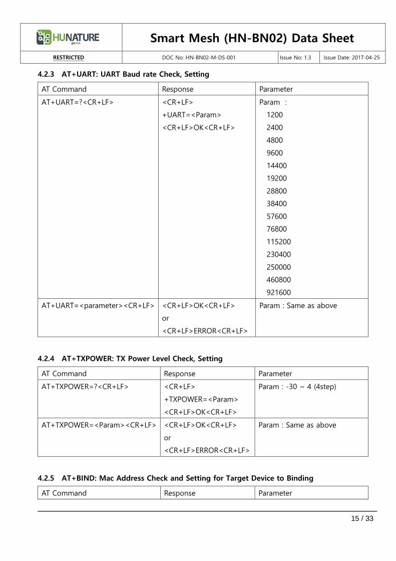
4.2.3 AT+UART: UART Baud rate Check, Setting
AT Command Response Parameter
AT+UART=?<CR+LF> <CR+LF>
+UART=<Param>
<CR+LF>OK<CR+LF>
Param :
1200
2400
4800
9600
14400
19200
28800
38400
57600
76800
115200
230400
250000
460800
921600
AT+UART=<parameter><CR+LF> <CR+LF>OK<CR+LF>
or
<CR+LF>ERROR<CR+LF>
Param : Same as above
4.2.4 AT+TXPOWER: TX Power Level Check, Setting
AT Command Response Parameter
AT+TXPOWER=?<CR+LF> <CR+LF>
+TXPOWER=<Param>
<CR+LF>OK<CR+LF>
Param : -30 ~ 4 (4step)
AT+TXPOWER=<Param><CR+LF> <CR+LF>OK<CR+LF>
or
<CR+LF>ERROR<CR+LF>
Param : Same as above
4.2.5 AT+BIND: Mac Address Check and Setting for Target Device to Binding
AT Command Response Parameter

Smart Mesh (HN-BN02) Data Sheet
RESTRICTED DOC No: HN-BN02-M-DS-001 Issue No: 1.3 Issue Date: 2017-04-25
16 / 33
AT+BIND=?<CR+LF> <CR+LF>
+BIND=<Param>
<CR+LF>OK<CR+LF>
Param : Mac Address (Hex)
예) 12,34,56,78,9a,bc
AT+BIND=<Param><CR+LF> <CR+LF>OK<CR+LF>
or
<CR+LF>ERROR<CR+LF>
Param : Same as above
4.2.6 AT+CMODE: Connection Mode Check, Setting
AT Command Response Parameter
AT+CMODE=?<CR+LF> <CR+LF>
+CMODE=<Param>
<CR+LF>OK<CR+LF>
Param :
“A” : can connect to all
devices
“U”: only connect to the
binding device
AT+CMODE=<Param><CR+LF> <CR+LF>OK<CR+LF>
or
<CR+LF>ERROR<CR+LF>
Param : Same as above
4.2.7 AT+NAME: Device Name Check, Setting
AT Command Response Parameter
AT+NAME =?<CR+LF> <CR+LF>
+NAME=<Param>
<CR+LF>OK<CR+LF>
Param :
AT+NAME=<Param><CR+LF> <CR+LF>OK<CR+LF>
or
<CR+LF>ERROR<CR+LF>
Param : less than 20 byte
4.2.8 AT+SERIAL: Serial Number Check, Setting
AT Command Response Parameter
AT+SERIAL=?<CR+LF> <CR+LF>
+SERIAL=<Param>
<CR+LF>OK<CR+LF>
Param : less than 10 byte
AT+SERIAL=<Param><CR+LF> <CR+LF>OK<CR+LF> Param : Same as above

Smart Mesh (HN-BN02) Data Sheet
RESTRICTED DOC No: HN-BN02-M-DS-001 Issue No: 1.3 Issue Date: 2017-04-25
17 / 33
or
<CR+LF>ERROR<CR+LF>
4.2.9 AT+MINCINT: Minimum Connection Interval Check, Setting
AT Command Response Parameter
AT+MINCINT=?<CR+LF> <CR+LF>
+MINCINT=<Param>
<CR+LF>OK<CR+LF>
Param :
10 < param < 1024
AT+MINCINT=<Param><CR+LF> <CR+LF>OK<CR+LF>
or
<CR+LF>ERROR<CR+LF>
Param : Same as above
4.2.10 AT+MAXCINT: Maximum Connection Interval Check, Setting
AT Command Response Parameter
AT+MAXCINT=?<CR+LF> <CR+LF>
+MAXCINT=<Param>
<CR+LF>OK<CR+LF>
Param :
10 < param < 1024
AT+MAXCINT=<Param><CR+LF> <CR+LF>OK<CR+LF>
or
<CR+LF>ERROR<CR+LF>
Param : Same as above
4.2.11 AT+ADVINT: Beacon advertise Interval Check, Setting
AT Command Response Parameter
AT+ADVINT=?<CR+LF> <CR+LF>
+ADVINT=<Param>
<CR+LF>OK<CR+LF>
Param :
100 < param < 1024
AT+ADVINT=<Param><CR+LF> <CR+LF>OK<CR+LF>
or
<CR+LF>ERROR<CR+LF>
Param : Same as above
4.2.12 AT+BEACON: Beacon Service On/Off
AT Command Response Parameter
AT+BEACON=?<CR+LF> <CR+LF> Param :

Smart Mesh (HN-BN02) Data Sheet
RESTRICTED DOC No: HN-BN02-M-DS-001 Issue No: 1.3 Issue Date: 2017-04-25
18 / 33
+BEACON=<Param>
<CR+LF>OK<CR+LF>
“ON” : On
“OFF” : Off
AT+BEACON=<Param><CR+LF> <CR+LF>OK<CR+LF>
or
<CR+LF>ERROR<CR+LF>
Param : Same as above
4.2.13 AT+MAJOR: Beacon Major ID Check, Setting
AT Command Response Parameter
AT+MAJOR=?<CR+LF> <CR+LF>
+MAJOR=<Param>
<CR+LF>OK<CR+LF>
Param : 0~65535
AT+MAJOR=<Param><CR+LF> <CR+LF>OK<CR+LF>
or
<CR+LF>ERROR<CR+LF>
Param : Same as above
4.2.14 AT+MINOR: Beacon Minor ID Check, Setting
AT Command Response Parameter
AT+MINOR=?<CR+LF> <CR+LF>
+MINOR=<Param>
<CR+LF>OK<CR+LF>
Param : 0~65535
AT+MINOR=<Param><CR+LF> <CR+LF>OK<CR+LF>
or
<CR+LF>ERROR<CR+LF>
Param : Same as above
4.2.15 AT+UUID: Beacon UUID Check, Setting
AT Command Response Parameter
AT+UUID=?<CR+LF> <CR+LF>
+UUID=<Param>
<CR+LF>OK<CR+LF>
Param : UUID 16 bytes (Hex)
예) 12,34,56,78,9a,bc,~ 16bytes
AT+UUID=<Param><CR+LF> <CR+LF>OK<CR+LF>
or
<CR+LF>ERROR<CR+LF>
Param : Same as above

Smart Mesh (HN-BN02) Data Sheet
RESTRICTED DOC No: HN-BN02-M-DS-001 Issue No: 1.3 Issue Date: 2017-04-25
19 / 33
4.2.16 AT+MPOWER: RSSI Measured Power Check, Setting of Beacon Advertise data
AT Command Response Parameter
AT+MPOWER =?<CR+LF> <CR+LF>
+MPOWER=<Param>
<CR+LF>OK<CR+LF>
Param :
AT+MPOWER=<Param><CR+LF> <CR+LF>OK<CR+LF>
or
<CR+LF>ERROR<CR+LF>
Param :
4.2.17 AT+DIMMER: Dimmer Service On/Off
AT Command Response Parameter
AT+DIMMER=?<CR+LF> <CR+LF>
+DIMMER=<Param>
<CR+LF>OK<CR+LF>
Param :
“ON” : On
“OFF” : Off
AT+DIMMER=<Param><CR+LF> <CR+LF>OK<CR+LF>
or
<CR+LF>ERROR<CR+LF>
Param : Same as above
4.2.18 AT+GID: Group ID Check, Setting of Dimmer Service
AT Command Response Parameter
AT+GID=?<CR+LF> <CR+LF>
+GID=<Param>
<CR+LF>OK<CR+LF>
Param : 0000 ~ FFFF (hex)
AT+GID=<Param><CR+LF> <CR+LF>OK<CR+LF>
or
<CR+LF>ERROR<CR+LF>
Param : Same as above
4.2.19 AT+PWM: LED PWM Check, Setting of Dimmer Service
AT Command Response Parameter
AT+PWM=?<CR+LF> <CR+LF>
+PWM=<Param>
<CR+LF>OK<CR+LF>
Param : R,G,B (00~64 (hex)
예) 30,30,30
AT+PWM=<Param><CR+LF> <CR+LF>OK<CR+LF> Param : Same as above

Smart Mesh (HN-BN02) Data Sheet
RESTRICTED DOC No: HN-BN02-M-DS-001 Issue No: 1.3 Issue Date: 2017-04-25
20 / 33
or
<CR+LF>ERROR<CR+LF>
4.2.20 AT+REPEATER: Repeater On/Off
AT Command Response Parameter
AT+ REPEATER=?<CR+LF> <CR+LF>
+REPEATER=<Param>
<CR+LF>OK<CR+LF>
Param :
“ON” : On
“OFF” : Off
AT+REPEATER=<Param><CR+LF> <CR+LF>OK<CR+LF>
or
<CR+LF>ERROR<CR+LF>
Param : Same as above
4.2.21 AT+MAC: Mac Address Check
AT Command Response Parameter
AT+MAC=?<CR+LF> <CR+LF>
+MAC=<Param>
<CR+LF>OK<CR+LF>
Param : Mac Address (Hex)
예) 12,34,56,78,9a,bc
4.2.22 AT+RSSI: RSSI Check
AT Command Response Parameter
AT+RSSI=?<CR+LF> <CR+LF>
+RSSI=<Param>
<CR+LF>OK<CR+LF>
4.2.23 AT+VER: Version Check
AT Command Response Parameter
AT+RSSI=?<CR+LF> <CR+LF>
+RSSI=<Param>
<CR+LF>OK<CR+LF>
4.2.24 AT+PASSWD: Password Setting
AT Command Response Parameter
Smart Mesh (HN-BN02) Data Sheet
RESTRICTED DOC No: HN-BN02-M-DS-001 Issue No: 1.3 Issue Date: 2017-04-25
21 / 33
AT+PASSWD=<Param><CR+LF> <CR+LF>OK<CR+LF>
or
<CR+LF>ERROR<CR+LF>
Param : less than 12 byte
Description: confirm password
and proceed
4.2.25 AT+SAVE: Save Setting Value
AT Command Response Parameter
AT+SAVE<CR+LF> <CR+LF>OK<CR+LF>
or
<CR+LF>ERROR<CR+LF>
Description
: confirm password and
proceed
4.2.26 AT+RESET: BLE Module Reset
AT Command Response Parameter
AT+RESET<CR+LF> <CR+LF>OK<CR+LF>
4.2.27 AT+ECHO: AT Command Echo On/Off
AT Command Response Parameter
AT+ECHO =?<CR+LF> <CR+LF>
+ECHO=<Param>
<CR+LF>OK<CR+LF>
Param :
“ON” : On
“OFF” : Off
AT+ECHO=<Param><CR+LF> <CR+LF>OK<CR+LF>
or
<CR+LF>ERROR<CR+LF>
Param : Same as above
4.2.28 AT+EXIT: AT Command mode exit
AT Command Response Parameter
AT+EXIT<CR+LF> <CR+LF>OK<CR+LF>

Smart Mesh (HN-BN02) Data Sheet
RESTRICTED DOC No: HN-BN02-M-DS-001 Issue No: 1.3 Issue Date: 2017-04-25
22 / 33
4.3 AT Command Example
4.3.1 UART to BLE Transmission test in Central, Peripheral mode

Smart Mesh (HN-BN02) Data Sheet
RESTRICTED DOC No: HN-BN02-M-DS-001 Issue No: 1.3 Issue Date: 2017-04-25
23 / 33
4.3.2 Beacon Mode Movement

Smart Mesh (HN-BN02) Data Sheet
RESTRICTED DOC No: HN-BN02-M-DS-001 Issue No: 1.3 Issue Date: 2017-04-25
24 / 33
5. Antenna Radiation Report
The Antenna 3D Radiation pattern and the measurement result of HN-BN module are as shown
below.
Picture 5-1 3D Radiation pattern & Test setup
Frequency 2442 MHz
Efficiency 83.75 %
Average Gain -0.77 dBi
Peak Gain 5.56 dBi
Table 5-1 Antenna test result

Smart Mesh (HN-BN02) Data Sheet
RESTRICTED DOC No: HN-BN02-M-DS-001 Issue No: 1.3 Issue Date: 2017-04-25
25 / 33
6. PCB Artwork Recommendation
When performing the PCB Artwork for target products of HN-BN Module, for optimum RF
performance, you need to secure 3mm of Copper Clearance area based on Chip Antenna
location as shown in below Picture 6-1.
Picture 6-1 3D Radiation pattern & Test setup
The position of HN module placed on the Target PCB needs to be located at the end of PCB
not middle, and the Antenna of Module must be located at the very end of PCB.

Smart Mesh (HN-BN02) Data Sheet
RESTRICTED DOC No: HN-BN02-M-DS-001 Issue No: 1.3 Issue Date: 2017-04-25
26 / 33
7. Packing
We safely wrap the product to protect it from storage, vibration from travelling, and impact
This product is packaged in Reel unit, and the 500 modules are packaged in one Reel.

Smart Mesh (HN-BN02) Data Sheet
RESTRICTED DOC No: HN-BN02-M-DS-001 Issue No: 1.3 Issue Date: 2017-04-25
27 / 33
8. Appendix 1 - Gender Board (HN-BN02-G)
This module is a board that provides the scalability of the Smart Mesh (HN-BN02-M) module,
it consists of a 2.54mm Pitch I/O and a Serial Wire Debug (SWD) Connector, as shown in Picture
8-1 below.
Picture 8-1 Gender Board
8.1 Pin Out
The pin configuration of BLE blocks is shown in Picture 8-2 below.
Picture 8-2 Pin out Diagram

Smart Mesh (HN-BN02) Data Sheet
RESTRICTED DOC No: HN-BN02-M-DS-001 Issue No: 1.3 Issue Date: 2017-04-25
28 / 33
8.2 Pin Configuration
Table 8.2-1 Pin Configuration
No Pin Name Type Description HN-BN02-M
Pin Assignment
1 GND Ground Ground (0V) PAD01 & PAD18
2 VDD Power 3.3VDC Power Supply Voltage PAD02
3 P00 I/O General Purpose I/O (AIN) PAD03
4 P01 I/O General Purpose I/O (AIN) PAD04
5 P02 I/O General Purpose I/O (AIN) PAD05
6 P03 I/O General Purpose I/O (AIN) PAD06
7 P04 I/O General Purpose I/O (AIN) PAD07
8 P05 I/O General Purpose I/O (AIN) PAD08
9 P06 I/O General Purpose I/O (AIN) PAD09
10 P07 I/O General Purpose I/O (AIN) PAD10
11 P08 I/O General Purpose I/O (DIO) PAD11
12 P09 I/O UART TX (DIO) PAD12
13 P10 I/O General Purpose I/O (DIO) PAD13
14 P11 I/O UART RX (DIO) PAD14
15 P16 I/O General Purpose I/O (DIO) PAD15
16 SWDIO I/O Serial Wire Debug (SWDIO/nRESET) PAD16
17 SWDCLK Input Serial Wire Debug (SWDCLK) PAD17
18 VDD Power 3.3VDC Power Supply Voltage PAD02
19 GND Ground Ground (0V) PAD01 & PAD18
20 GND Ground Ground (0V) PAD01 & PAD18
21 SWDIO (J3) I/O Serial Wire Debug (SWDIO/nRESET) PAD16
22 SWDCLK (J3) Input Serial Wire Debug (SWDCLK) PAD17
23 GND (J3) Ground Ground (0V) PAD01 & PAD18
Smart Mesh (HN-BN02) Data Sheet
RESTRICTED DOC No: HN-BN02-M-DS-001 Issue No: 1.3 Issue Date: 2017-04-25
29 / 33
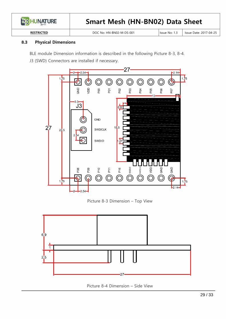
8.3 Physical Dimensions
BLE module Dimension information is described in the following Picture 8-3, 8-4.
J3 (SWD) Connectors are installed if necessary.
Picture 8-3 Dimension – Top View
Picture 8-4 Dimension – Side View

Smart Mesh (HN-BN02) Data Sheet
RESTRICTED DOC No: HN-BN02-M-DS-001 Issue No: 1.3 Issue Date: 2017-04-25
30 / 33
9. Appendix II – Development Kit (HN-DK-01)
This module is a board which provides a development environment using HN-BN02, HN-SO01
module, providing Debug and External Interface (Serial). It is a board attached with a Light
Sensor (CDS), Motion Sensor (PIR), and RGB LED (RGB), and it consists of 2.54 mm I/O and a
USB-C Connector. Using the HN-DK board, various applications can be developed, such as
Beacon, Mesh Network, Motion Sensor, Light Sensor, LED Dimming, and RGB Lighting Control,
and interlocking with a separate external sensor module is possible.
Picture 9-1 HN-DK Board
9.1 Pin Out
The pin configuration of BLE blocks is shown in Picture 9-2 below.
Picture 9-2 Pin out Diagram

Smart Mesh (HN-BN02) Data Sheet
RESTRICTED DOC No: HN-BN02-M-DS-001 Issue No: 1.3 Issue Date: 2017-04-25
31 / 33
9.2 Pin Configuration
Table 9.2-1 Pin Configuration
No Pin Name Type Description Remark
1 VDD5.0 Power 5.0VDC Power Supply Voltage J4
2 GND Ground Ground (0V) J4
3 SW1 Input Pull-Down Switch Input (AIN) J4
4 SW2 Input Pull-Down Switch Input (AIN) J4
5 LED_R I/O LED (Red) J4
6 LED_G I/O LED (Green) J4
7 LED_B I/O LED (Blue) J4
8 PAD08 I/O General Purpose I/O (DIO) J4
9 CDS Input CDS Sensor (AIN) J4
10 T_OUT I/O PIR Sensor (DIO) J4
11 GND Ground Ground (0V) J2
12 VDD Power 3.3VDC Power Supply Voltage J2
13 SW1 Input Pull-Down Switch Input (AIN) J2
14 SW2 Input Pull-Down Switch Input (AIN) J2
15 LED_R I/O LED (Red) J2
16 LED_G I/O LED (Green) J2
17 LED_B I/O LED (Blue) J2
18 PAD08 I/O General Purpose I/O (DIO) J2
19 CDS Input CDS Sensor (AIN) J2
20 T_OUT I/O PIR Sensor (DIO) J2
21 PAD11
UART_RTS I/O
(Normal) General Purpose I/O (DIO)
(Option) UART_RTS J3
22 UART_TXD I/O UART TX (DIO) J3
23 PAD13
UART_CTS I/O
(Normal) General Purpose I/O (DIO)
(Option) UART_CTS J3
24 UART_RXD I/O UART RX (DIO) J3

Smart Mesh (HN-BN02) Data Sheet
RESTRICTED DOC No: HN-BN02-M-DS-001 Issue No: 1.3 Issue Date: 2017-04-25
32 / 33
25 MOTION I/O PIR Sensor (DIO) J3
26 SWDIO I/O Serial Wire Debug (SWDIO/nRESET) J3
27 SWDCLK Input Serial Wire Debug (SWDCLK) J3
28 VDD Power 3.3VDC Power Supply Voltage J3
29 GND Ground Ground (0V) J3
30 GND Ground Ground (0V) J3
31 PAD11
UART_RTS I/O
(Normal) General Purpose I/O (DIO)
(Option) UART_RTS J5
32 UART_TXD_EXT I/O UART TX External (Control by SW4) J5
33 PAD13
UART_CTS I/O
(Normal) General Purpose I/O (DIO)
(Option) UART_CTS J5
34 UART_RXD_EXT I/O UART RX External (Control by SW4) J5
35 MOTION I/O PIR Sensor (DIO) J5
36 SWDIO I/O Serial Wire Debug (SWDIO/nRESET) J5
37 SWDCLK Input Serial Wire Debug (SWDCLK) J5
38 VDD Power 3.3VDC Power Supply Voltage J5
39 GND Ground Ground (0V) J5
40 GND Ground Ground (0V) J5

Smart Mesh (HN-BN02) Data Sheet
RESTRICTED DOC No: HN-BN02-M-DS-001 Issue No: 1.3 Issue Date: 2017-04-25
33 / 33
9.3 Physical Dimensions
The Dimension information of DK Board is described in the following Picture 9-3, 9-4.
Picture 9-3 Dimension – Top View
Picture 9-4 Dimension – Side View