Embed Size (px)
Citation preview
2.1 VTPS62730
V = 2.1 VOUT
CC1120
at 169 MHz
Balun and Antenna
Connector
2.3 to 3.9 V
RF matching
TI DesignsSmart Grid wM-Bus RF Subsystem at 169 MHz
TI Designs Design FeaturesTI Designs provide the foundation that you need • Low-Power 169-MHz, wM-Bus RF Deviceincluding methodology, testing and design files to • Market-Leading, RF-Blocking, Selectivity, andquickly evaluate and customize the system. TI Designs RX-Sensitivity Solution for 169 MHzhelp you accelerate your time to market.
• ETSI Category 1 Receiver-Capable RF SystemDesign Resources • No Costly SAW Filter Required
• No Costly TCXO RequiredTool Folder Containing Design FilesTIDC-WMBUS-169MHz
• Supports Multiple Battery TechnologiesCC1120 Product Folder (LiSoCl2, LiMnO2, and Others)TPS62730 Product Folder
Featured Applications• Smart Flow Meters (Gas, Water, and Heat)ASK Our E2E Experts
WEBENCH® Calculator Tools • Data Collectors with 169-MHz wM-Bus• Narrow-Band Applications for Tracking, Tracing,
and Meter Reading• Social Alarms in the 169-MHz ETSI Band
An IMPORTANT NOTICE at the end of this TI reference design addresses authorized use, intellectual property matters and otherimportant disclaimers and information.
Windows is a registered trademark of Microsoft Corporation.R&S is a registered trademark of Rohde & Schwarz GmbH & Co.All other trademarks are the property of their respective owners.
1TIDU512–September 2014 Smart Grid wM-Bus RF Subsystem at 169 MHzSubmit Documentation Feedback
Copyright © 2014, Texas Instruments Incorporated
Key System Specifications www.ti.com
1 Key System SpecificationsCC1120 operates from 2 to 3.6 V (3.9 V is the absolute maximum value). The transmit current for 15 dBmof TX power (conducted measurement) is typically 54 mA at 3.3-V supply. The input supply voltagecoming from the battery or power management system should be more than 2.1 V to provide the best RFperformance of the CC1120 radio.
Supported data rates are from 0 to 200 kbps and the device supports 2-FSK, 2-GFSK, 4-FSK, 4-GFSK,MSK, and OOK modulation formats. 2-GFSK and 4-GFSK are required to comply with the wM-Bus N-modes at 169 MHz.
The BOM has been optimized for the 169-MHz band. This design uses no SAW filter and no TCXOcomponents and is targeted at ETSI Category 1, receiver-compliant wM-Bus systems. Adding an externalSAW component is possible and a good practice in many applications.
In addition to low-cost XTAL devices, CC1120 also supports TCXO components for applications thatmandate the highest-possible frequency accuracy over temperature and lifetime, such as gas or watermeters.
To achieve the lowest energy consumption with CC1120, the TPS62730 with a fixed 2.1-V output hasbeen selected. The input voltage range for this DC-DC converter is from 1.9 to 3.9 V and a 30 nA (typical)ultra-low power bypass mode is integrated. The TPS62730 automatically enters bypass mode once thebattery voltage falls below the transition threshold VIT BYP.
Table 1. Energy Consumption
MIN TYP MAX UNITAutomatic bypass switch transition ON/falling VIN 2.14 2.20 2.3
VIT BYP threshold (activation/deactivation) TPS62730 (2.1 V) VOFF/rising VIN 2.19 2.25 2.35ON/BYP = High
The DC-DC converter is available in a very-small 1 × 1.5 mm2, 6-pin QFN package. The converterachieves up to 95% DC-DC efficiency and can provide up to 100-mA output current, using up to 3-MHzswitching frequency.
CC1120 uses a VQFN32 package of 5 × 5 mm with a ground pad.
The operating ambient temperature for both CC1120 and TPS62730 is TA = –40°C to 85°C.
2 Smart Grid wM-Bus RF Subsystem at 169 MHz TIDU512–September 2014Submit Documentation Feedback
Copyright © 2014, Texas Instruments Incorporated
www.ti.com System Description
2 System DescriptionCC1120 is targeted at systems with ETSI Category 1 Compliance in 169-MHz and 433-MHz bands andoffers a high spectral efficiency (9.6 kbps in 12.5-kHz channel in compliance with FCC narrow-bandingmandate). CC1120 delivers market-leading blocking, selectivity, and sensitivity RF performance numbersin all supported ISM bands.
This design is focused specifically on 169-MHz wM-Bus systems, as defined for the smart gas metersrollout in Italy and France.
Using a supply voltage of up to 3.6 V delivers excellent RF results. However, the drawback is increasedpower loss in the internal LDOs of CC1120. To reduce these losses and extend the battery life in such anRF system, TI recommends to use the lowest-possible supply voltage.
Another consideration is that the supply voltage must be the same for both MCUs running the RFcommunication protocol (for example, the wM-Bus N2-mode RF stack) and the CC1120 radio. The supplyvoltage must be the same to avoid voltage level issues on the SPI and on the control signals between theradio and the MCU.
These considerations lead to the choice of TPS62730 with 2.1-V output for this design (TPS62733 with2.3-V fixed output is also available).
Depending on the application’s duty cycle (for example, how many transmit and receive operations perday, how long each of these operations is, and at which transmit power level), a different power schemewill be most efficient. In wM-Bus capable gas or water meters, as used in Italy and France, the transmitoperations occur just a few times per day. For these meters, the recommended solution for the highestpower savings is to shut down the CC1120 device completely during the inactivity time. The power-up andinitialization procedure of CC1120 takes just a few milliseconds and can be easily repeated every time thedevice starts from shutdown. In other cases with much higher duty cycles, using the power-down modewith register retention (a typical value is 120 nA) may be the better option.
The combination of TPS62730 plus the CC1120 radio delivers a RF solution, which is market-leading interms of both RF performance and low-power consumption. The design has been developed to meet andexceed the requirements of all wM-Bus systems at 169 MHz, which are becoming popular in Europe forsmart flow meters.
Additionally, due to the CC1120 excellent blocking and selectivity performance (see ETSI category 1receiver requirements in ETSI EN 300 220-2), this CC1120-based solution is perfectly suited for use insocial alarms and data tracking systems.
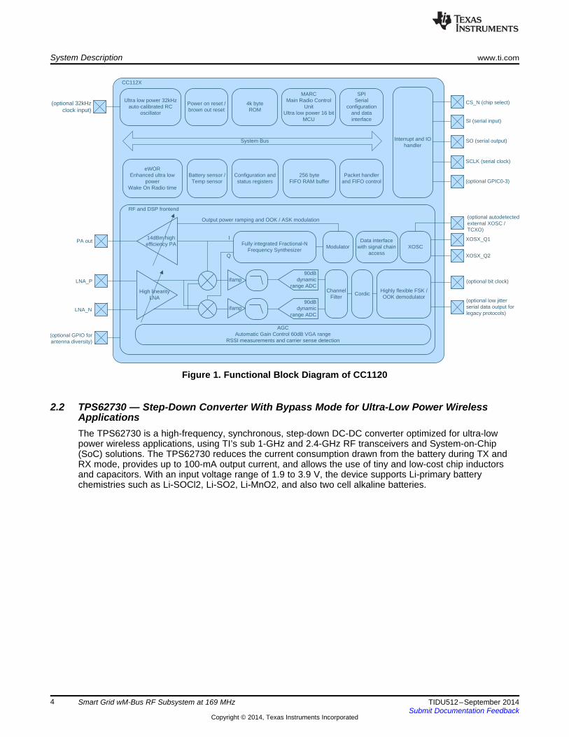
2.1 CC1120 — High-Performance RF Transceiver for Narrow-Band SystemsThe CC1120 transceiver features adjacent channel selectivity of 64 dB at 12.5-kHz offset and blockingperformance of 91 dB at 10-MHz offset in combination with excellent receiver sensitivity of –123 dBm at1.2 kbps.
In transmit mode, the CC1120 transforms the data packets created in the MCU into RF signal and passesthe RF signal to the antenna. In receive mode, the CC1120 receives RF signal from the antenna, detectsthe bit stream, and converts the bits into data bytes, which are passed to the MCU for further processing.
3TIDU512–September 2014 Smart Grid wM-Bus RF Subsystem at 169 MHzSubmit Documentation Feedback
Copyright © 2014, Texas Instruments Incorporated
90dB dynamic
range ADC
90dB dynamic
range ADC
High linearity LNA
AGCAutomatic Gain Control 60dB VGA range
RSSI measurements and carrier sense detection
CordicChannel
FilterHighly flexible FSK / OOK demodulator
XOSCData interface
with signal chain access
ModulatorFully integrated Fractional-N
Frequency Synthesizer
eWOREnhanced ultra low
powerWake On Radio time
Battery sensor / Temp sensor
Configuration and status registers
256 byteFIFO RAM buffer
Packet handler and FIFO control
Interrupt and IO handler
SPISerial
configurationand data interface
MARCMain Radio Control
UnitUltra low power 16 bit
MCU
4k byteROM
Power on reset / brown out reset
Ultra low power 32kHzauto-calibrated RC
oscillator
System Bus
RF and DSP frontend
Output power ramping and OOK / ASK modulation
CC112X
PA out
LNA_P
LNA_N
(optional GPIO for antenna diversity)
CS_N (chip select)
SI (serial input)
SO (serial output)
SCLK (serial clock)
(optional GPIC0-3)
(optional autodetected external XOSC / TCXO)
XOSX_Q1
XOSX_Q2
(optional bit clock)
(optional low jitter serial data output for legacy protocols)
14dBm high efficiency PA
ifamp
ifamp
I
Q
(optional 32kHz clock input)
System Description www.ti.com
Figure 1. Functional Block Diagram of CC1120
2.2 TPS62730 — Step-Down Converter With Bypass Mode for Ultra-Low Power WirelessApplicationsThe TPS62730 is a high-frequency, synchronous, step-down DC-DC converter optimized for ultra-lowpower wireless applications, using TI’s sub 1-GHz and 2.4-GHz RF transceivers and System-on-Chip(SoC) solutions. The TPS62730 reduces the current consumption drawn from the battery during TX andRX mode, provides up to 100-mA output current, and allows the use of tiny and low-cost chip inductorsand capacitors. With an input voltage range of 1.9 to 3.9 V, the device supports Li-primary batterychemistries such as Li-SOCl2, Li-SO2, Li-MnO2, and also two cell alkaline batteries.
4 Smart Grid wM-Bus RF Subsystem at 169 MHz TIDU512–September 2014Submit Documentation Feedback
Copyright © 2014, Texas Instruments Incorporated
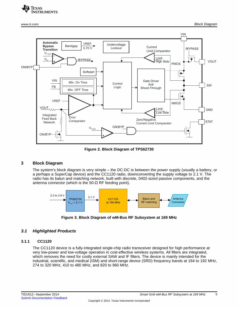
2.1 VTPS62730
V = 2.1 VOUT
CC1120
at 169 MHz
Balun and Antenna
Connector
2.3 to 3.9 V
RF matching
Gate DriverAnti
Shoot-Through
Current
Limit Comparator
SW
Softstart
Bandgap UndervoltageLockout
LimitHigh Side
Limit
Low Side
VOUT
ON/BYP
VIN
GND
Min. On Time
Min. OFF Time
VIN
ON/BYP
IntegratedFeed BackNetwork
VREF
FB
ErrorComparator Zero/Negative
Current Limit Comparator
ControlLogic
PMOS
NMOS
VREF
0.70 V
VOUT
/BYPASS
VIT BYP
VIN /BYPASS
VTSTAT
+
-
+
-
STAT
AutomaticBypassTransition
ON/BYP
www.ti.com Block Diagram
Figure 2. Block Diagram of TPS62730
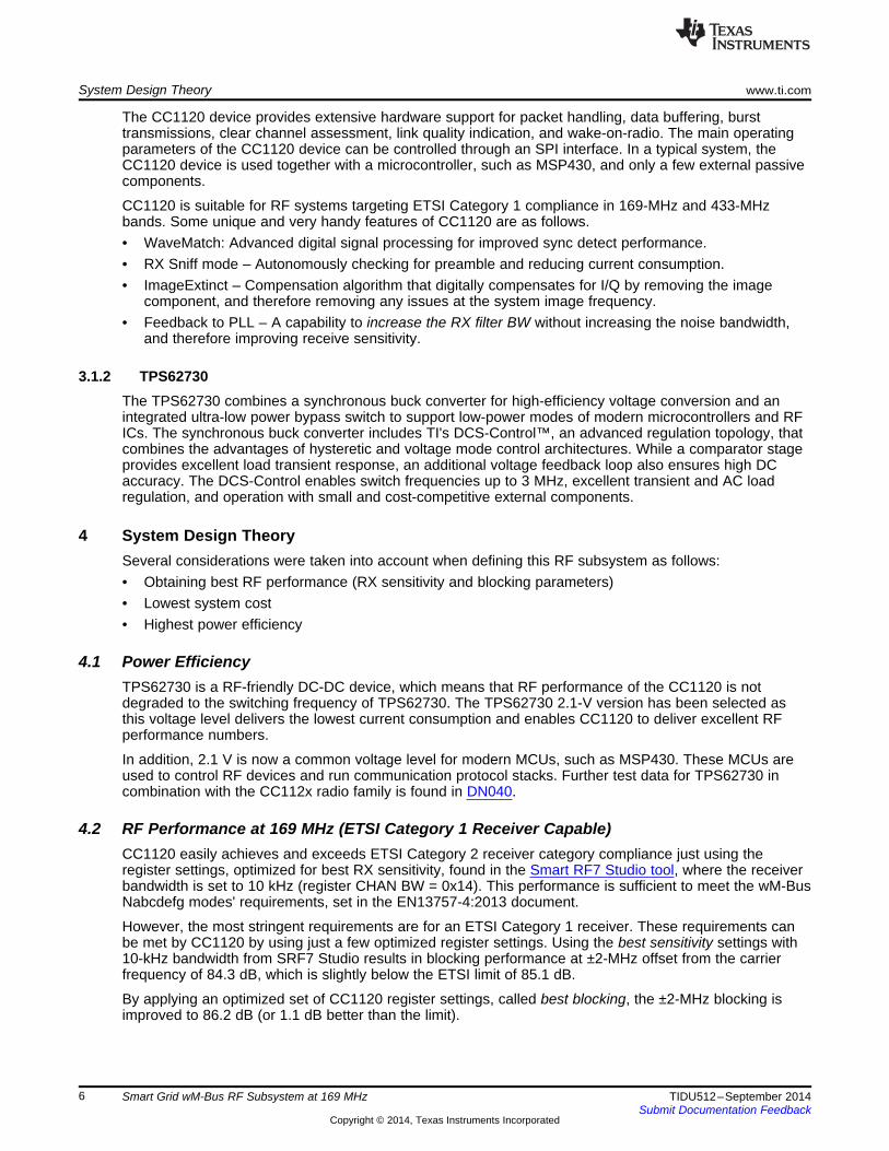
3 Block DiagramThe system’s block diagram is very simple – the DC-DC is between the power supply (usually a battery, ora perhaps a SuperCap device) and the CC1120 radio, downconverting the supply voltage to 2.1 V. Theradio has its balun and matching network, built with discrete, 0402-sized passive components, and theantenna connector (which is the 50-Ω RF feeding point).
Figure 3. Block Diagram of wM-Bus RF Subsystem at 169 MHz
3.1 Highlighted Products
3.1.1 CC1120The CC1120 device is a fully-integrated single-chip radio transceiver designed for high performance atvery low-power and low-voltage operation in cost-effective wireless systems. All filters are integrated,which removes the need for costly external SAW and IF filters. The device is mainly intended for theindustrial, scientific, and medical (ISM) and short-range device (SRD) frequency bands at 164 to 192 MHz,274 to 320 MHz, 410 to 480 MHz, and 820 to 960 MHz.
5TIDU512–September 2014 Smart Grid wM-Bus RF Subsystem at 169 MHzSubmit Documentation Feedback
Copyright © 2014, Texas Instruments Incorporated
System Design Theory www.ti.com
The CC1120 device provides extensive hardware support for packet handling, data buffering, bursttransmissions, clear channel assessment, link quality indication, and wake-on-radio. The main operatingparameters of the CC1120 device can be controlled through an SPI interface. In a typical system, theCC1120 device is used together with a microcontroller, such as MSP430, and only a few external passivecomponents.
CC1120 is suitable for RF systems targeting ETSI Category 1 compliance in 169-MHz and 433-MHzbands. Some unique and very handy features of CC1120 are as follows.• WaveMatch: Advanced digital signal processing for improved sync detect performance.• RX Sniff mode – Autonomously checking for preamble and reducing current consumption.• ImageExtinct – Compensation algorithm that digitally compensates for I/Q by removing the image
component, and therefore removing any issues at the system image frequency.• Feedback to PLL – A capability to increase the RX filter BW without increasing the noise bandwidth,
and therefore improving receive sensitivity.
3.1.2 TPS62730The TPS62730 combines a synchronous buck converter for high-efficiency voltage conversion and anintegrated ultra-low power bypass switch to support low-power modes of modern microcontrollers and RFICs. The synchronous buck converter includes TI's DCS-Control™, an advanced regulation topology, thatcombines the advantages of hysteretic and voltage mode control architectures. While a comparator stageprovides excellent load transient response, an additional voltage feedback loop also ensures high DCaccuracy. The DCS-Control enables switch frequencies up to 3 MHz, excellent transient and AC loadregulation, and operation with small and cost-competitive external components.
4 System Design TheorySeveral considerations were taken into account when defining this RF subsystem as follows:• Obtaining best RF performance (RX sensitivity and blocking parameters)• Lowest system cost• Highest power efficiency
4.1 Power EfficiencyTPS62730 is a RF-friendly DC-DC device, which means that RF performance of the CC1120 is notdegraded to the switching frequency of TPS62730. The TPS62730 2.1-V version has been selected asthis voltage level delivers the lowest current consumption and enables CC1120 to deliver excellent RFperformance numbers.
In addition, 2.1 V is now a common voltage level for modern MCUs, such as MSP430. These MCUs areused to control RF devices and run communication protocol stacks. Further test data for TPS62730 incombination with the CC112x radio family is found in DN040.
4.2 RF Performance at 169 MHz (ETSI Category 1 Receiver Capable)CC1120 easily achieves and exceeds ETSI Category 2 receiver category compliance just using theregister settings, optimized for best RX sensitivity, found in the Smart RF7 Studio tool, where the receiverbandwidth is set to 10 kHz (register CHAN BW = 0x14). This performance is sufficient to meet the wM-BusNabcdefg modes' requirements, set in the EN13757-4:2013 document.
However, the most stringent requirements are for an ETSI Category 1 receiver. These requirements canbe met by CC1120 by using just a few optimized register settings. Using the best sensitivity settings with10-kHz bandwidth from SRF7 Studio results in blocking performance at ±2-MHz offset from the carrierfrequency of 84.3 dB, which is slightly below the ETSI limit of 85.1 dB.
By applying an optimized set of CC1120 register settings, called best blocking, the ±2-MHz blocking isimproved to 86.2 dB (or 1.1 dB better than the limit).
6 Smart Grid wM-Bus RF Subsystem at 169 MHz TIDU512–September 2014Submit Documentation Feedback
Copyright © 2014, Texas Instruments Incorporated
www.ti.com System Design Theory
NOTE: These excellent blocking numbers are achieved without a costly external SAW filtercomponent.
The trade-off for getting ETSI Category 1 receiver compliance and improved blocking numbers is that theRX sensitivity is reduced from –120 dB to –116 dB.
It has been confirmed in field measurements that the channel noise at 169 MHz in some European areascan be significantly higher, close to –110 or even –100 dB. In such cases, having two optimized registersets, which differ by only a few registers values, a CC1120-based 169-MHz RF system can dynamicallyadapt to the changing RF channel conditions in the field. This dynamic adaption is enabled by a periodicmeasurement of the channel noise level and switching between the best sensitivity or best blockingsettings, based on the RSSI levels measured over time.
4.3 System CostIn high-volume rollouts of 169-MHz RF systems in Europe, the total system cost (and also the BOM cost)is of the utmost importance. Achieving the ETSI Category 1 receiver performance is already quitechallenging. However, achieving the performance without external TCXO and without an external SAWfilter is even better. CC1120-based designs are also leading not only in RF performance, but also in termsof system cost, as TCXO and SAW filters are not needed. In addition, no external LNA device is requiredto meet the RX sensitivity requirements at 169 MHz for France.
7TIDU512–September 2014 Smart Grid wM-Bus RF Subsystem at 169 MHzSubmit Documentation Feedback
Copyright © 2014, Texas Instruments Incorporated
Getting Started Hardware www.ti.com
5 Getting Started HardwareThe test hardware comprises two PCBs: the TRXEB platform from the CC1120DK and the CC1120 plusTPS62730 evaluation board. Two existing TPS62730 plus CC1120EM at 868-MHz boards have beenmodified (BOM component changes only) to support 169 MHz. All reported results were measuredconducted, which means using a RF cable connection between the R&S® RF signal generator and theDUT (the RF boards).
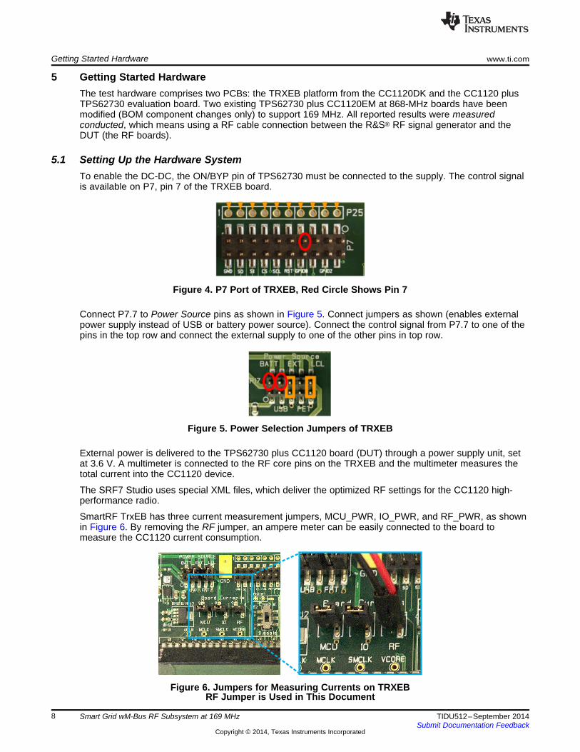
5.1 Setting Up the Hardware SystemTo enable the DC-DC, the ON/BYP pin of TPS62730 must be connected to the supply. The control signalis available on P7, pin 7 of the TRXEB board.
Figure 4. P7 Port of TRXEB, Red Circle Shows Pin 7
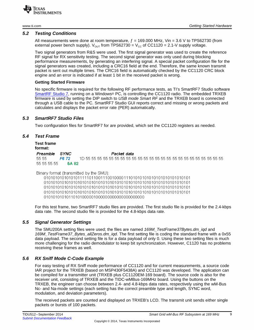
Connect P7.7 to Power Source pins as shown in Figure 5. Connect jumpers as shown (enables externalpower supply instead of USB or battery power source). Connect the control signal from P7.7 to one of thepins in the top row and connect the external supply to one of the other pins in top row.
Figure 5. Power Selection Jumpers of TRXEB
External power is delivered to the TPS62730 plus CC1120 board (DUT) through a power supply unit, setat 3.6 V. A multimeter is connected to the RF core pins on the TRXEB and the multimeter measures thetotal current into the CC1120 device.
The SRF7 Studio uses special XML files, which deliver the optimized RF settings for the CC1120 high-performance radio.
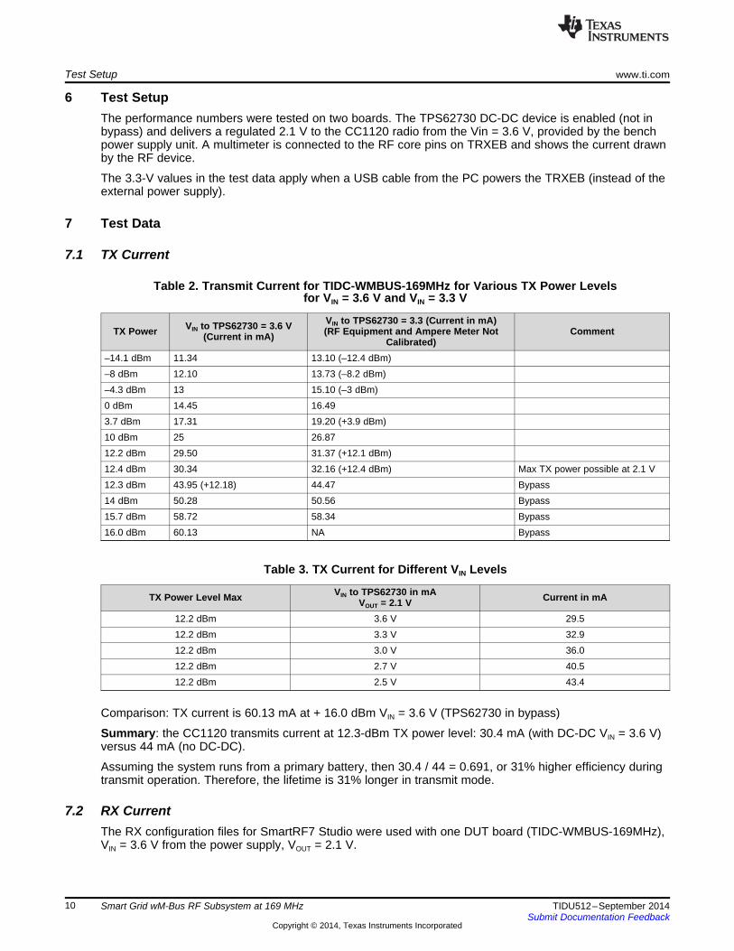
SmartRF TrxEB has three current measurement jumpers, MCU_PWR, IO_PWR, and RF_PWR, as shownin Figure 6. By removing the RF jumper, an ampere meter can be easily connected to the board tomeasure the CC1120 current consumption.
Figure 6. Jumpers for Measuring Currents on TRXEBRF Jumper is Used in This Document
8 Smart Grid wM-Bus RF Subsystem at 169 MHz TIDU512–September 2014Submit Documentation Feedback
Copyright © 2014, Texas Instruments Incorporated
www.ti.com Getting Started Hardware
5.2 Testing ConditionsAll measurements were done at room temperature, ƒ = 169.000 MHz, Vin = 3.6 V to TPS62730 (fromexternal power bench supply). VOUT from TPS62730 = VCC of CC1120 = 2.1-V supply voltage.
Two signal generators from R&S were used. The first signal generator was used to create the referenceRF signal for RX sensitivity testing. The second signal generator was only used during blockingperformance measurements, by generating an interfering signal. A special packet configuration file for thesignal generators was created, including a CRC16 field at the end. Therefore, the same known transmitpacket is sent out multiple times. The CRC16 field is automatically checked by the CC1120 CRC blockengine and an error is indicated if at least 1 bit in the received packet is wrong.
Getting Started FirmwareNo specific firmware is required for the following RF performance tests, as TI’s SmartRF7 Studio softwareSmartRF Studio 7, running on a Windows® PC, is controlling the CC1120 radio. The embedded TRXEBfirmware is used by setting the DIP switch to USB mode Smart RF and the TRXEB board is connectedthrough a USB cable to the PC. SmartRF7 Studio GUI reports correct and missing or wrong packets andcalculates and displays the packet error rate (PER) automatically.
5.3 SmartRF7 Studio FilesTwo configuration files for SmartRF7 for are provided, which set the CC1120 registers as needed.
5.4 Test FrameTest frameformat:
For this test frame, two SmartRF7 studio files are provided. The first studio file is provided for the 2.4-kbpsdata rate. The second studio file is provided for the 4.8-kbps data rate.
5.5 Signal Generator SettingsThe SMU200A setting files were used; the files are named 169M_TestFrame37Bytes.dm_iqd and169M_TestFrame37_Bytes_allZeros.dm_iqd. The first setting file is coding the standard frame with a 0x55data payload. The second setting file is for a data payload of only 0. Using these two setting files is muchmore challenging for the radio demodulator to keep bit synchronization. However, C1120 has no problemsreceiving these frames as well.
5.6 RX Sniff Mode C-Code ExampleFor easy testing of RX Sniff mode performance of CC1120 and for current measurements, a source codeIAR project for the TRXEB (based on MSP430F5438A) and CC1120 was developed. The application canbe compiled for a transmitter unit (TRXEB plus CC1120EM-169 board). The source code is also for thereceiver unit, consisting of TRXEB and the TIDC-wMBus-169MHz board. Using the buttons on theTRXEB, the engineer can choose between 2.4- and 4.8-kbps data rates, respectively using the wM-BusNc- and Na-mode settings (each setting has the correct preamble type and length, SYNC word,modulation, and deviation parameters).
The received packets are counted and displayed on TRXEB’s LCD. The transmit unit sends either singlepackets or bursts of 100 packets.
9TIDU512–September 2014 Smart Grid wM-Bus RF Subsystem at 169 MHzSubmit Documentation Feedback
Copyright © 2014, Texas Instruments Incorporated
Test Setup www.ti.com
6 Test SetupThe performance numbers were tested on two boards. The TPS62730 DC-DC device is enabled (not inbypass) and delivers a regulated 2.1 V to the CC1120 radio from the Vin = 3.6 V, provided by the benchpower supply unit. A multimeter is connected to the RF core pins on TRXEB and shows the current drawnby the RF device.
The 3.3-V values in the test data apply when a USB cable from the PC powers the TRXEB (instead of theexternal power supply).
7 Test Data
7.1 TX Current
Table 2. Transmit Current for TIDC-WMBUS-169MHz for Various TX Power Levelsfor VIN = 3.6 V and VIN = 3.3 V
VIN to TPS62730 = 3.3 (Current in mA)VIN to TPS62730 = 3.6 VTX Power (RF Equipment and Ampere Meter Not Comment(Current in mA) Calibrated)–14.1 dBm 11.34 13.10 (–12.4 dBm)–8 dBm 12.10 13.73 (–8.2 dBm)–4.3 dBm 13 15.10 (–3 dBm)0 dBm 14.45 16.493.7 dBm 17.31 19.20 (+3.9 dBm)10 dBm 25 26.8712.2 dBm 29.50 31.37 (+12.1 dBm)12.4 dBm 30.34 32.16 (+12.4 dBm) Max TX power possible at 2.1 V12.3 dBm 43.95 (+12.18) 44.47 Bypass14 dBm 50.28 50.56 Bypass15.7 dBm 58.72 58.34 Bypass16.0 dBm 60.13 NA Bypass
Table 3. TX Current for Different VIN Levels
VIN to TPS62730 in mATX Power Level Max Current in mAVOUT = 2.1 V12.2 dBm 3.6 V 29.512.2 dBm 3.3 V 32.912.2 dBm 3.0 V 36.012.2 dBm 2.7 V 40.512.2 dBm 2.5 V 43.4
Comparison: TX current is 60.13 mA at + 16.0 dBm VIN = 3.6 V (TPS62730 in bypass)
Summary: the CC1120 transmits current at 12.3-dBm TX power level: 30.4 mA (with DC-DC VIN = 3.6 V)versus 44 mA (no DC-DC).
Assuming the system runs from a primary battery, then 30.4 / 44 = 0.691, or 31% higher efficiency duringtransmit operation. Therefore, the lifetime is 31% longer in transmit mode.
7.2 RX CurrentThe RX configuration files for SmartRF7 Studio were used with one DUT board (TIDC-WMBUS-169MHz),VIN = 3.6 V from the power supply, VOUT = 2.1 V.
10 Smart Grid wM-Bus RF Subsystem at 169 MHz TIDU512–September 2014Submit Documentation Feedback
Copyright © 2014, Texas Instruments Incorporated
www.ti.com Test Data
Table 4. RX Sniff Currents at VIN = 3.6 V
RX Sniff Mode VIN to TPS62730 = 3.6 V VIN = 3.6 VData Rate TPS62730 = 3.6 V Normal Mode Bypass Mode Normal RX Mode Comment
(Current in mA) (Current in mA) (Current in mA)Data packetsPHY-WM2400 10.5 13.20 22.45 999/1000 OK
PHY-WM2400 8.5 13.54 23.08 No data packetsData packetsPHY-WM4800 10.0 13.35 22.76 999/1000 OK
PHY-WM4800 10.0 13.72 23.28 No data packets
Comparison: CC1120 RX current = 23 mA at 3.6 V
Summary: The CC1120 receive current when using TPS62730 is reduced from 23 to 13.5 mA, whichequals 13.5 / 23 = 0.5869 or 41% higher efficiency during receive. Therefore, the lifetime is 41% longer inreceive operation.
Enabling RX sniff mode, which is working for 2.4- and 4.8-kbps wM-Bus modes at 169 MHz, can drive theaverage receive current consumption to approximately 10 mA if a 3.6-V external supply voltage isprovided.
7.3 RX Current With Sniff Mode EnabledRX Sniff mode, which can reduce the current consumption without sacrificing RF performance, has beentested for both PHY-WM2400 and PHY-WM4800 (used in France) and Ncd and Nabef modes (used inItaly).
RX Sniff mode uses another feature of CC1120 called Wavematch, which uses on-chip DSP circuitry tolock onto the incoming waveform. The on-chip advantage is much faster settling the receiver. Therefore,the result is lower current consumption. RX Sniff mode is a feature that automatically duty cycles the radioand quickly triggers on either RSSI or preamble conditions. Triggering on RSSI or carrier sense (CS) isfaster and gives the lowest average power consumption (if there is no RF noise), so this method has beenimplemented in the software example.
Table 5. Average RX Current Consumption in RX Sniff Mode in PHY-WM2400 and PHY-WM4800
Triggering On RSSI, Triggering On RSSIPreambleData Rate CC1120EM-169 With TPS62730 CommentsBytes (No TPS62730) CS = –116 dBm2.4 kb/s GFSK = PHY-WM2400 2 13.8 mA 8.5 mA Using RX Sniff code project4.8 kb/s GFSK = PHY-WM4800 2 18.0 mA 10.0 mA Using RX Sniff code project
Note that the values in Table 5 can be achieved only if the RF channel is noise free or if the noise level isbelow the RX sensitivity limit, which is set in the CC1120. This limit is called the CS threshold and can beadjusted as needed by the application through the AGC_CS_THRESHOLD register field found in theAGC_CS_THR register. The AGC_CS_THRESHOLD field is a 2's complement number with 1-dBresolution and is given by Equation 1.
CS Threshold = AGC_CS_THR + RSSI Offset
where• RSSI Offset of CC1120 = –102 dBm (1)
7.4 RX SensitivityA test packet of 31 bytes payload plus 2 bytes CRC has been used. The CRC bytes were adjusted so theCC1120 hardware block checks the CRC16 sum and reports error or OK status automatically. Thecorresponding XML configuration file for SmartRF7 Studio is loaded and puts the RF board in RX mode.The proper IQD configuration file for the RF signal generator (CMU) is loaded and used as the TXreference packet.
11TIDU512–September 2014 Smart Grid wM-Bus RF Subsystem at 169 MHzSubmit Documentation Feedback
Copyright © 2014, Texas Instruments Incorporated
Test Data www.ti.com
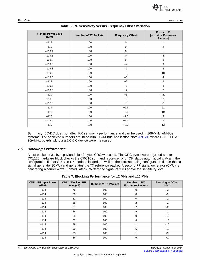
Table 6. RX Sensitivity versus Frequency Offset Variation
Errors in %RF Input Power Level Number of TX Packets Frequency Offset [= Lost or Erroneous(dBm) Packets]–118 100 0 1–119 100 0 2
–119.4 100 0 1–119.5 100 0 4–119.7 100 0 9–119.5 100 –2 9–119.3 100 –2 2–119.3 100 –3 18–118.5 100 –3 4–119 100 +2 2
–119.5 100 +2 8–119.3 100 +2 7–119 100 +3 >20
–118.5 100 +3 31–117.5 100 +3 21–119 100 +2.5 22–118 100 +2.5 10–118 100 +2.3 3
–118.5 100 +2.3 2–119 100 +2.3 13
Summary: DC-DC does not affect RX sensitivity performance and can be used in 169-MHz wM-Bussystems. The achieved numbers are inline with TI wM-Bus Application Note AN121, where CC1120EM-169-MHz boards without a DC-DC device were measured.
7.5 Blocking PerformanceA test packet of 31-byte payload plus 2-bytes CRC was used. The CRC bytes were adjusted so theCC1120 hardware block checks the CRC16 sum and reports error or OK status automatically. Again, theconfiguration file for SRF7 in RX mode is loaded, as well as the corresponding configuration file for the RFsignal generator (CMU) and generates the TX reference packet. A second RF signal generator (CMU) isgenerating a carrier wave (unmodulated) interference signal at 3 dB above the sensitivity level.
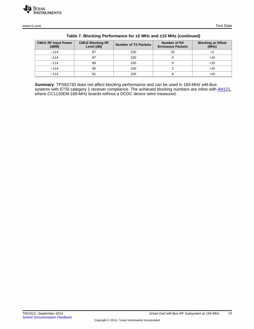
Table 7. Blocking Performance for ±2 MHz and ±10 MHz
CMU1 RF Input Power CMU2 Blocking RF Number of RX Blocking at OffsetNumber of TX Packets(dBM) Level (dB) Erroneous Packets (MHz)–114 75 100 0 –2–114 80 100 0 –2–114 82 100 0 –2–114 85 100 2 –2–114 87 100 21 –2–114 86 100 9 –2–114 85 100 0 –10–114 87 100 0 –10–114 89 100 1 –10–114 90 100 6 –10–114 85 100 1 +2–114 86 100 6 +2
12 Smart Grid wM-Bus RF Subsystem at 169 MHz TIDU512–September 2014Submit Documentation Feedback
Copyright © 2014, Texas Instruments Incorporated
www.ti.com Test Data
Table 7. Blocking Performance for ±2 MHz and ±10 MHz (continued)CMU1 RF Input Power CMU2 Blocking RF Number of RX Blocking at OffsetNumber of TX Packets(dBM) Level (dB) Erroneous Packets (MHz)
–114 87 100 25 +2–114 87 100 0 +10–114 89 100 0 +10–114 90 100 2 +10–114 91 100 8 +10
Summary: TPS62730 does not affect blocking performance and can be used in 169-MHz wM-Bussystems with ETSI category 1 receiver compliance. The achieved blocking numbers are inline with AN121,where CC1120EM-169-MHz boards without a DCDC device were measured.
13TIDU512–September 2014 Smart Grid wM-Bus RF Subsystem at 169 MHzSubmit Documentation Feedback
Copyright © 2014, Texas Instruments Incorporated
Test Data www.ti.com
14 Smart Grid wM-Bus RF Subsystem at 169 MHz TIDU512–September 2014Submit Documentation Feedback
Copyright © 2014, Texas Instruments Incorporated
www.ti.com Design Files
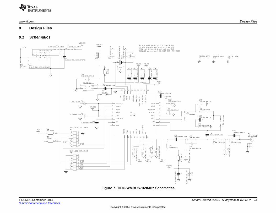
8 Design Files
8.1 Schematics
Figure 7. TIDC-WMBUS-169MHz Schematics
15TIDU512–September 2014 Smart Grid wM-Bus RF Subsystem at 169 MHzSubmit Documentation Feedback
Copyright © 2014, Texas Instruments Incorporated
Design Files www.ti.com
16 Smart Grid wM-Bus RF Subsystem at 169 MHz TIDU512–September 2014Submit Documentation Feedback
Copyright © 2014, Texas Instruments Incorporated
www.ti.com Design Files
8.2 Bill of MaterialsTo download the bill of materials (BOM), see the design files at TIDC-WMBUS-169MHz.
Table 8. BOM of TIDC-WMBUS-169MHz
ITEM QTY REFERENCE VALUE PART MANUFACTURER PARTNUMBER ALTERNATE PCB NOTEDESCRIPTION PART FOOTPRINT
U1 1 CC1120 CC1120 TI Transceiver TI N/A N/A N/A N/AC302 1 C_0402 Capacitor,
general, 0402;Do not mount
C177 1 C_1P2_0402_NP Capacitor, 1p2, Capacitor Murata GRM1555C1H1 04020_B_50 0402, NP0, +/- R2BZ01D
0.1pF 50VC321 1 C_100N_0402_X Do not mount Capacitor 0402
5R_K_10C172;C173 2 C_100P_0402_N Capacitor, 100p, Capacitor Murata GRM1555C1H10 0402
P0_J_50 0402, NP0, 5% 1JZ01D50V
C171;C211 2 C_10N_0402_X7 Capacitor, 10n, Capacitor Murata GRM155R71E10 0402R_K_25 0402, X7R, 10%, 3KA01D
25VC2 1 C_1210 Capacitor, Capacitor
general, 1210C174 1 C_82P_0402_NP Capacitor, 82p, Capacitor Murata GRM1555C1H82 0402
0_J_50 0402, NP0, 5% 0JZ01D50V
C301;C311;C175 3 C_15P_0402_NP Capacitor, 15p, Capacitor Murata GRM1555C1H15 04020_J_50 0402, NP0, 5%, 0JA01D
50VC231 1 C_1N8_0402_U2 Capacitor, 1n8, Capacitor Murata GRM1557U1A18 0402
J_J_10 0402, U2J, 5%, 2JA01D10V
C61 1 C_220N_0402_X Capacitor, 220n, Capacitor Murata GRM155R61A22 04025R_K_10 0402, X5R, 10%, 4KE19D
10VC322 1 C_22P_0402_NP Do not mount Capacitor Murata GRM1555C1H22 0402
0_J_50 0JZ01DC201; C191; 3 C_12P_0402_NP Capacitor, 12p, Capacitor Murata GRM1555C1H12 0402C181 0_J_50 0402, NP0, 5%, 0JA01D
50VC10;C13 2 C_2U2_0402_X5 Capacitor, 2u2, Capacitor 0402
R_M_6P3VDC 0402, X5R, +/-20%, 6.3V
17TIDU512–September 2014 Smart Grid wM-Bus RF Subsystem at 169 MHzSubmit Documentation Feedback
Copyright © 2014, Texas Instruments Incorporated
Design Files www.ti.com
Table 8. BOM of TIDC-WMBUS-169MHz (continued)ITEM QTY REFERENCE VALUE PART MANUFACTURER PARTNUMBER ALTERNATE PCB NOTE
DESCRIPTION PART FOOTPRINTC176 1 C_12P_0402_NP Capacitor, 12p, Capacitor Murata GRM1555C1H12 0402
0_J_50 0402, NP0, 5%, 0JA01D50V
C11;C51;C121;C 11 C_47N_0402_X7 Capacitor, 47n, Capacitor Murata GRM155R71E47 0402131;C151;C221; R_K_25 0402, X7R, 10%, 3KA88DC251;C261;C271 25V;C281;C291;L192;L201 2 L_82N_0402_J_ Inductor, 82n, Inductor Murata LQW15AN82NJ0 0402
LQW 0402, ±5%, wire- 0wound type
L174 1 L_68N_0402_J_ Inductor, 68n, Inductor Murata LQW15AN68NJ0 0402LQW 0402, ±5%, wire- 0
wound typeL172 1 L_18N_0402_J_ Inductor, 18n, Inductor Murata LQW15AN18NJ0 0402
LQW 0402, ±5%, wire- 0Dwound type
L191 1 L_150N_0402_J Inductor, 150n, Inductor Murata LQG15HSR15J0 04020402, ±5% 2
L193 1 L_39N_0402_J_ Inductor, 39n, Inductor Murata LQW15AN39NJ0 0402LQW 0402, ±5%, wire- 0D
wound typeL173 1 L_100N_0402_J Inductor, 100n, Inductor Murata LQW15ANR10J0 0402
_LQW 0402, ±5%, wire- 0wound type
L3 1 L_2U2_0805_N_ Inductor, 2u2, Inductor Murata LQM21PN2R2N 0805LQM21 0805, ±30% GC
L171 1 L_220N_0402_J Inductor, 220n, Inductor Murata LQG15HSR22J0 04020402, ±5% 2
L2 1 L_BEAD_102_04 EMI filter bead, Filter bead Murata BLM15HG102SN 040202 0402 1k ohms 1D
Tape GHz BandGen Use
R1;R321 2 R_0402 Resistor, Resistor 0402general, 0402;Do not mount
R12 (edited 1 R_0_0402 Resistor, 0 ohm, Resistor Koa RK73Z1ETTP 0402manually) 0402R322 1 R_0_0402 Do not mount Resistor 0402R2 1 R_0_0402 Resistor, 0 ohm, Resistor Koa RK73Z1ETTP 0402
0402
18 Smart Grid wM-Bus RF Subsystem at 169 MHz TIDU512–September 2014Submit Documentation Feedback
Copyright © 2014, Texas Instruments Incorporated
www.ti.com Design Files
Table 8. BOM of TIDC-WMBUS-169MHz (continued)ITEM QTY REFERENCE VALUE PART MANUFACTURER PARTNUMBER ALTERNATE PCB NOTE
DESCRIPTION PART FOOTPRINTR171 1 R_22_0402_J Resistor, 22 Resistor Koa RK73H1ETTP22 0402
ohms, 0402, 5% R0F (±1%)R141 1 R_56K_0402_F Resistor, 56k Resistor Koa RK73H1ETTP56 0402
ohms, 0402, 02F±1%
P3 1 SMA_SMD SMA connector, Connector Hus-Tsan Group SMA-10V21-straight SMD- Taiwan TGGmount
P1-2 2 SMD_SOCKET_ SMD pinrow Connector Samtec SFM-110-02-SM-2X10 socket, .050 D-A-K-TR
spacing, 2x10X2 1 TG_5021CG Do not mount TCXO Epson Toyocom TG_5021CGU3 1 TPS62730 Step Down TI DC-DC TI TPS62730DRY
Converter with converterBypass Mode
X1 1 X_32.000/10/20/ Crystal, XTAL NDK, Epson60/10 32.000000MHz,
FA-128, 10.0pF,+/-10ppm, (FTC:+/-20ppm at -40/85C), 60ohms
19TIDU512–September 2014 Smart Grid wM-Bus RF Subsystem at 169 MHzSubmit Documentation Feedback
Copyright © 2014, Texas Instruments Incorporated
Design Files www.ti.com
8.3 Layout GuidelinesCopy the layout exactly as shown in the Gerber files as it has been optimized for best RF performance;the RF subsystem is using a 4-layer PCB. Find additional information on PCB layout considerations in theTI documents AN098 and AN068.
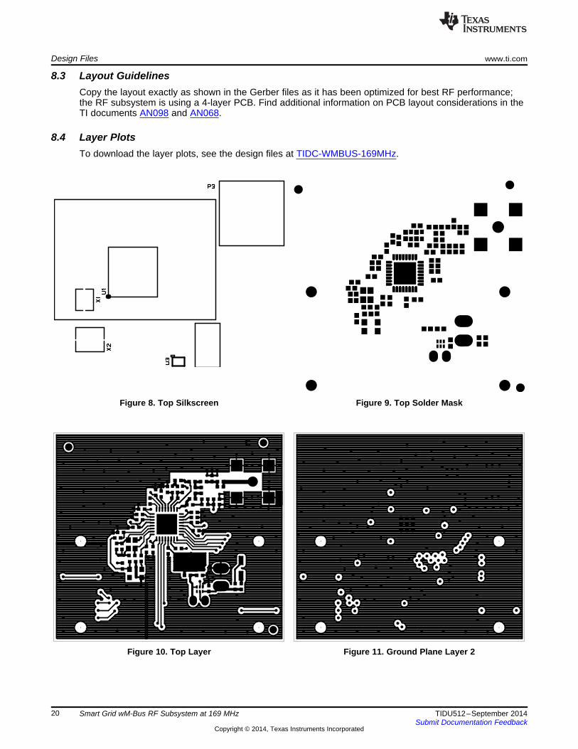
8.4 Layer PlotsTo download the layer plots, see the design files at TIDC-WMBUS-169MHz.
Figure 8. Top Silkscreen Figure 9. Top Solder Mask
Figure 10. Top Layer Figure 11. Ground Plane Layer 2
20 Smart Grid wM-Bus RF Subsystem at 169 MHz TIDU512–September 2014Submit Documentation Feedback
Copyright © 2014, Texas Instruments Incorporated
www.ti.com Design Files
Figure 12. Power Plane Layer 3 Figure 13. Bottom Layer 4
Figure 14. Bottom Solder Mask Figure 15. Bottom Silkscreen
21TIDU512–September 2014 Smart Grid wM-Bus RF Subsystem at 169 MHzSubmit Documentation Feedback
Copyright © 2014, Texas Instruments Incorporated
Design Files www.ti.com
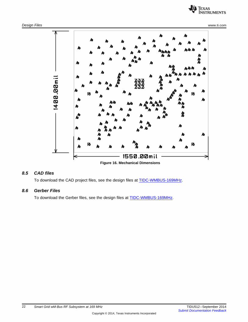
Figure 16. Mechanical Dimensions
8.5 CAD filesTo download the CAD project files, see the design files at TIDC-WMBUS-169MHz.
8.6 Gerber FilesTo download the Gerber files, see the design files at TIDC-WMBUS-169MHz.
22 Smart Grid wM-Bus RF Subsystem at 169 MHz TIDU512–September 2014Submit Documentation Feedback
Copyright © 2014, Texas Instruments Incorporated
www.ti.com Design Files
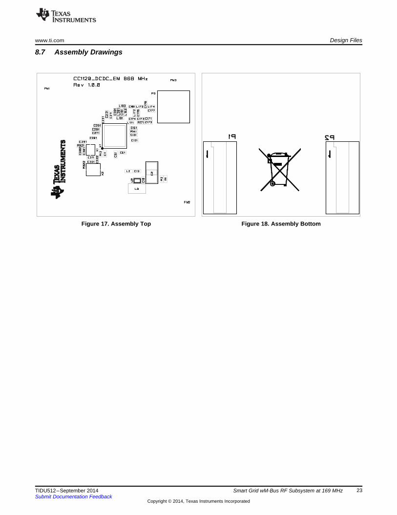
8.7 Assembly Drawings
Figure 17. Assembly Top Figure 18. Assembly Bottom
23TIDU512–September 2014 Smart Grid wM-Bus RF Subsystem at 169 MHzSubmit Documentation Feedback
Copyright © 2014, Texas Instruments Incorporated
Design Files www.ti.com
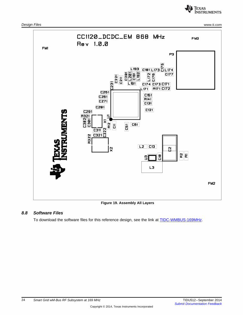
Figure 19. Assembly All Layers
8.8 Software FilesTo download the software files for this reference design, see the link at TIDC-WMBUS-169MHz.
24 Smart Grid wM-Bus RF Subsystem at 169 MHz TIDU512–September 2014Submit Documentation Feedback
Copyright © 2014, Texas Instruments Incorporated
www.ti.com References
9 References
1. CC1120 data sheet, CC1120 High-Performance RF Transceiver for Narrowband Systems, CC11202. TPS62730 data sheet, Step-Down Converter with Bypass Mode for Ultra Low Power Wireless
Applications, TPS627303. Application Note AN121, Wireless M-Bus Implementation with CC112x / CC120x High Performance
Transceiver Family, AN1214. Design Note DN040, Reduced Battery Current Using CC112x/CC1175/CC1200 with TPS62730,
DN0405. European Standard, ETSI EN 300 220-2 V2.4.1 (2012-05), ETSI EN 300 220-26. Application Note AN098, Layout Review Techniques for Low Power RF Designs, AN0987. Application Note AN068, Adapting TI LPRF Reference Designs for Layer Stacking, AN0688. SmartRF Studio 7, SmartRF Studio 79. Application Report CC112x/CC120x, CC112x/CC120x RX Sniff Mode, CC112x/CC120x
10 TerminologyETSI Category 1 Receiver—Definition for most stringent set of RF parameters in EN300 220 v2.4.1
N-mode— The wM-Bus mode at 169 MHz, selected for Italy and France smart gas meter rollout, withminor changes respectively
wM-Bus— The European RF Metering standard, providing solutions for 169-, 433-, and 868-MHz bands
25TIDU512–September 2014 Smart Grid wM-Bus RF Subsystem at 169 MHzSubmit Documentation Feedback
Copyright © 2014, Texas Instruments Incorporated
About the Author www.ti.com
11 About the AuthorMILEN STEFANOV is a system applications engineer at Texas Instruments, where he is responsible forSub-1-GHz RF communications solutions for smart meters. Milen has significantly contributed to deliveringTI’s full wM-Bus system solution, consisting of MCU + RF chipset, a complete wM-Bus protocol stack, anda dedicated power management solution. Milen has system-level expertise on smart metering and RFcommunications and more than 15 years of experience working with customers. He has published severaltechnical articles on wM-Bus-related topics in the past four years. He earned his master of science inelectrical engineering (MSEE) from Technical University in Chemnitz, Germany.
26 Smart Grid wM-Bus RF Subsystem at 169 MHz TIDU512–September 2014Submit Documentation Feedback
Copyright © 2014, Texas Instruments Incorporated
IMPORTANT NOTICE FOR TI REFERENCE DESIGNS
Texas Instruments Incorporated ("TI") reference designs are solely intended to assist designers (“Buyers”) who are developing systems thatincorporate TI semiconductor products (also referred to herein as “components”). Buyer understands and agrees that Buyer remainsresponsible for using its independent analysis, evaluation and judgment in designing Buyer’s systems and products.TI reference designs have been created using standard laboratory conditions and engineering practices. TI has not conducted anytesting other than that specifically described in the published documentation for a particular reference design. TI may makecorrections, enhancements, improvements and other changes to its reference designs.Buyers are authorized to use TI reference designs with the TI component(s) identified in each particular reference design and to modify thereference design in the development of their end products. HOWEVER, NO OTHER LICENSE, EXPRESS OR IMPLIED, BY ESTOPPELOR OTHERWISE TO ANY OTHER TI INTELLECTUAL PROPERTY RIGHT, AND NO LICENSE TO ANY THIRD PARTY TECHNOLOGYOR INTELLECTUAL PROPERTY RIGHT, IS GRANTED HEREIN, including but not limited to any patent right, copyright, mask work right,or other intellectual property right relating to any combination, machine, or process in which TI components or services are used.Information published by TI regarding third-party products or services does not constitute a license to use such products or services, or awarranty or endorsement thereof. Use of such information may require a license from a third party under the patents or other intellectualproperty of the third party, or a license from TI under the patents or other intellectual property of TI.TI REFERENCE DESIGNS ARE PROVIDED "AS IS". TI MAKES NO WARRANTIES OR REPRESENTATIONS WITH REGARD TO THEREFERENCE DESIGNS OR USE OF THE REFERENCE DESIGNS, EXPRESS, IMPLIED OR STATUTORY, INCLUDING ACCURACY ORCOMPLETENESS. TI DISCLAIMS ANY WARRANTY OF TITLE AND ANY IMPLIED WARRANTIES OF MERCHANTABILITY, FITNESSFOR A PARTICULAR PURPOSE, QUIET ENJOYMENT, QUIET POSSESSION, AND NON-INFRINGEMENT OF ANY THIRD PARTYINTELLECTUAL PROPERTY RIGHTS WITH REGARD TO TI REFERENCE DESIGNS OR USE THEREOF. TI SHALL NOT BE LIABLEFOR AND SHALL NOT DEFEND OR INDEMNIFY BUYERS AGAINST ANY THIRD PARTY INFRINGEMENT CLAIM THAT RELATES TOOR IS BASED ON A COMBINATION OF COMPONENTS PROVIDED IN A TI REFERENCE DESIGN. IN NO EVENT SHALL TI BELIABLE FOR ANY ACTUAL, SPECIAL, INCIDENTAL, CONSEQUENTIAL OR INDIRECT DAMAGES, HOWEVER CAUSED, ON ANYTHEORY OF LIABILITY AND WHETHER OR NOT TI HAS BEEN ADVISED OF THE POSSIBILITY OF SUCH DAMAGES, ARISING INANY WAY OUT OF TI REFERENCE DESIGNS OR BUYER’S USE OF TI REFERENCE DESIGNS.TI reserves the right to make corrections, enhancements, improvements and other changes to its semiconductor products and services perJESD46, latest issue, and to discontinue any product or service per JESD48, latest issue. Buyers should obtain the latest relevantinformation before placing orders and should verify that such information is current and complete. All semiconductor products are soldsubject to TI’s terms and conditions of sale supplied at the time of order acknowledgment.TI warrants performance of its components to the specifications applicable at the time of sale, in accordance with the warranty in TI’s termsand conditions of sale of semiconductor products. Testing and other quality control techniques for TI components are used to the extent TIdeems necessary to support this warranty. Except where mandated by applicable law, testing of all parameters of each component is notnecessarily performed.TI assumes no liability for applications assistance or the design of Buyers’ products. Buyers are responsible for their products andapplications using TI components. To minimize the risks associated with Buyers’ products and applications, Buyers should provideadequate design and operating safeguards.Reproduction of significant portions of TI information in TI data books, data sheets or reference designs is permissible only if reproduction iswithout alteration and is accompanied by all associated warranties, conditions, limitations, and notices. TI is not responsible or liable forsuch altered documentation. Information of third parties may be subject to additional restrictions.Buyer acknowledges and agrees that it is solely responsible for compliance with all legal, regulatory and safety-related requirementsconcerning its products, and any use of TI components in its applications, notwithstanding any applications-related information or supportthat may be provided by TI. Buyer represents and agrees that it has all the necessary expertise to create and implement safeguards thatanticipate dangerous failures, monitor failures and their consequences, lessen the likelihood of dangerous failures and take appropriateremedial actions. Buyer will fully indemnify TI and its representatives against any damages arising out of the use of any TI components inBuyer’s safety-critical applications.In some cases, TI components may be promoted specifically to facilitate safety-related applications. With such components, TI’s goal is tohelp enable customers to design and create their own end-product solutions that meet applicable functional safety standards andrequirements. Nonetheless, such components are subject to these terms.No TI components are authorized for use in FDA Class III (or similar life-critical medical equipment) unless authorized officers of the partieshave executed an agreement specifically governing such use.Only those TI components that TI has specifically designated as military grade or “enhanced plastic” are designed and intended for use inmilitary/aerospace applications or environments. Buyer acknowledges and agrees that any military or aerospace use of TI components thathave not been so designated is solely at Buyer's risk, and Buyer is solely responsible for compliance with all legal and regulatoryrequirements in connection with such use.TI has specifically designated certain components as meeting ISO/TS16949 requirements, mainly for automotive use. In any case of use ofnon-designated products, TI will not be responsible for any failure to meet ISO/TS16949.IMPORTANT NOTICE
Mailing Address: Texas Instruments, Post Office Box 655303, Dallas, Texas 75265Copyright © 2015, Texas Instruments Incorporated