Embed Size (px)
Citation preview
Small-signal Analysis and Design of Constant-on-
time V2 Control for Ceramic Caps
Shuilin Tian
Thesis submitted to the Faculty of the Virginia Polytechnic Institute and State University
in partial fulfillment of the requirements for the degree of
Master of Science
in Electrical Engineering
APPROVED
Fred C. Lee, Chair Paolo Mattavelli
Dushan Boroyevich
April 19th, 2012 Blacksburg, Virginia
Keywords: constant-on-time control, V2 control Digital control, small-signal analysis and design
© 2012, Shuilin Tian
Small-signal Analysis and Design of Constant-on-
time V2 Control for Ceramic Caps
Shuilin Tian
(Abstract)
Recently, constant-on-time V2 control is more and more popular in industry products due to
features of high light load efficiency, simple implementation and fast transient response. In many
applications such as cell phone, camera, and other portable devices, low-ESR capacitors such as
ceramic caps are preferred due to small size and small output voltage ripple requirement.
However, for the converters with ceramic caps, the conventional V2 control suffers from the sub-
harmonic oscillation due to the lagging phase of the capacitor voltage ripple relative to the
inductor current ripple. Two solutions to eliminate sub-harmonic oscillations are discussed in [39]
and the small-signal models are also derived based on time-domain describing function.
However, the characteristic of constant-on-time V2 with external ramp is not fully understood
and no explicit design guideline for the external ramp is provided. For digital constant on-time
V2 control, the high resolution PWM can be eliminated due to constant on-time modulation
scheme and direct output voltage feedback [43]. However, the external ramp design is not only
related to the amplitude of the limit-cycle oscillation, but also very important to the stability of
the system. The previous analysis is not thorough since numerical solution is used. The primary
objective of this work is to gain better understanding of the small-signal characteristic for analog
and digital constant-on-time V2 with ramp compensations, and provide the design guideline
based on the factorized small-signal model.
iii
First, constant on-time current-mode control and constant on-time V2 control are reviewed.
Generally speaking, constant-on-time current mode control does not have stability issues.
However, for constant-on-time V2 control with ceramic caps, sub-harmonic oscillation occurs
due to the lagging phase of the capacitor voltage ripple. External ramp compensation and current
ramp compensation are two solutions to solve the problem. Previous equivalent circuit model
extended by Ray Ridley’s sample-and-hold concept is not applicable since it fails to consider the
influence of the capacitor voltage ripple. The model proposed in [39] successfully considers the
influence from the capacitor voltage ripple by using time-domain describing function method.
However, the characteristic of constant-on-time V2 with external ramp is not fully understood.
Therefore, more research focusing on the analysis is needed to gain better understanding of the
characteristic and provide the design guideline for the ramp compensations.
After that, the small-signal model and design of analog constant on-time V2 control is
investigated and discussed. The small-signal models are factorized and pole-zero movements are
identified. It is found that with increasing the external ramp, two pairs of double poles first move
toward each other at half of switching frequency, after meeting at the key point, the two double
poles separate, one pair moves to a lower frequency and the other moves to a higher frequency
while keeping the quality factor equal to each other. For output impedance, with increasing the
external ramp, the low frequency magnitude also increases. The recommended external ramp is
around two times the magnitude at the key point K. When Duty cycle is larger, the damping
performance is not good with only external ramp compensation, unless very high switching
frequency is used. With current ramp compensation, it is recommended to design the current
iv
ramp so that the quality factor of the double pole is around 1. With current ramp compensation,
the damping can be well controlled regardless of the circuit parameters.
Next, the small-signal analysis and design strategy is also extended to digital constant on-
time V2 control structure which is proposed in [43]. It is found that the scenario is very similar as
analog constant on-time V2 control. The external ramp should be designed around the key point
to improve the dynamic performance. The sampling effects of the output voltage require a larger
external ramp to stabilize digital constant-on-time V2 control while suffers only a little bit of
damping performance. One simple method for measuring control-to-output transfer functions in
digital constant-on-time V2 control is presented. The experimental results verify the small-signal
analysis except for the high frequency phase difference which reveals the delay effects in the
circuit. Load transient experimental results prove the proposed design guideline for digital
constant on-time V2 control.
As a conclusion, the characteristics of analog and digital constant-on-time V2 control
structures are examined and design guidelines are proposed for ramp compensations based on the
factorized small-signal model. The analysis and design guideline are verified with simplis
simulation and experimental results.

v
Acknowledgments
First I would like to express my sincere gratitude to my advisor, Dr. Fred C. Lee, for his
advising, encouragement, and generous patience. It is him who leads me into the world of power
electronics. I have learned a lot from his extensive knowledge and his rigorous research attitude
during the past three years. He often shares his philosophy with me, which is the most beneficial
to me. His help has become my life-long heritage. Without his help, none of the results showing
here would be possible.
I am also grateful to my other committee members: Dr. Paolo Mattavelli and Dr. Dushan
Boroyevich. For Dr. Mattavelli, your rich knowledge and suggestions inspires me a lot. I would
like to thank you for all the discussions and all the great suggestions. For Dr. Dushan Boroyevich,
I would like to thank you for your support, suggestions and encouragement throughout this entire
process.
I would also like to thank all the great staff in CPES: Ms. Teresa Shaw, Ms. Linda Gallagher,
Ms. Marianne Hawthorne, Ms. Teresa Rose, Ms Linda Long, Mr. Doug Sterk, Mr. David Gilham,
and Dr. Wenli Zhang.
I am especially indebted to my colleagues in the VRM Group and Digital Control Group.
In particular, I would like to thank Dr. Jian Li, Dr. Brian Cheng, Mr. Feng Yu for their help and
time on my research. It has been a great pleasure to work with the talented, creative, helpful and
dedicated colleagues. I would like to thank all the students of our teams: Dr. Shuo Wang, Dr.
Dianbo Fu, Dr. Pengju Kong, Dr. Qiang Li, Dr. Brian Cheng, Dr. David Reusch, Mr. Daocheng
Huang, Mr. Pengjie Lai, Mr. Zijian Wang, Mr. Qian Li, Mr. Alex Ji, Mr. Chanwit

vi
Prasantanakorn, Mr. Mingkai Mu, Mr. Yingyi Yan , Mr. Haoran Wu, Mr. Feng Yu, Mr. Yipeng
Su, Mr. Weiyi Feng, Mr. Wei Zhang, Mr. Li Jiang, Mr. Zhiqiang Wang, Mr. Pei-Hsin Liu, Ms.
Le Du, Mr. Xiucheng Huang, Mr.Yang Jiao, Mr. Zhengyang Liu, Mr Yucheng Yang and Dr.
Dongbing Hou, Mr Sizhao Lu. I also would like to thank all the visiting scholars of our teams for
their suggestion and support: Dr. Yue Chang, Dr. Xiaoyong Ren, Dr. Fanghua Zhang, Dr.
Yuling Li, Dr. Feng Zheng, Dr. Xinke Wu, Mr. Jim Chen, Mr. Feng Wang, Dr Weijun Lei and
Mr Zeng Li. My thanks also go to all of the other students I have met in CPES: Dr. Xiao Cao,
Mr. Zheyuan Tan, Ms.Yiying Yao, Mr. Yin Wang, Mr. Li Jiang, Ms Han Cui, Mr. Kim,
Woochan, Mr. Tao Tao, Mr. Di Xu; Dr. Di Zhang, Dr. Puqi Ning, Dr. Fang Luo, Dr. Sara
Ahmad, Mr. Dong Jiang , Mr. Ruxi Wang , Mr. Dong Dong, Mr. Zhiyu Shen, Mr. Zhen Chen,
Mr. Bo Wen, Mr Xuning Zhang, Mr. Jaksic, Marko, Mr. Danilovic, Milisav, Mr. Bishnoi,
Hemant, Mr. Justin Walraven, Mr. Jing Xue, Ms. Zhuxian Xu, Ms. Zheng Zhao; Mr. Lingxiao
Xue, Mr. Zhemin Zhang and Mr. Bo Zhou.
My deepest appreciation goes toward my family, my father Chunyong Tian, my mother
Qiu’e Gu and my sister Lijun Tian, who have always provided support and encouragement
throughout my further education. Thank you for the support over these years.

vii
This work was supported by the power management consortium(AcBel Polytech, Chicony
Power, Crane Aerospace, Delta Electronics, Emerson Network Power, Huawei Technologies,
International Rectifier, Intersil Corporation, Linear Technology, Lite-On Technology, Monolithic
Power Systems, National Semiconductor, NXP Semiconductors, Richtek Technology and Texas
Instruments), and the Engineering Research Center Shared Facilities supported by the National
Science Foundation under NSF Award Number EEC-9731677. Any opinions, findings and
conclusions or recommendations expressed in this material are those of the author and do not
necessarily reflect those of the National Science Foundation.
This work was conducted with the use of SIMPLIS software, donated in kind by Transim
Technology of the CPES Industrial Consortium.
viii
Table of Contents
Chapter 1. Introduction ................................................................................................................. 1
1.1 Review of Constant-on-time Current Mode Control ....................................................... 1
1.2 Research Background: Constant-on-time V2 Control ..................................................... 9
1.3 Thesis Outline .................................................................................................................... 19
Chapter 2. Small-signal Analysis and Design of Analog Constant-on-time V2 Control ........ 22
2.1 Previous Small-signal Model with External Ramp Compensation .............................. 22
2.2 Factorized Small-signal Model with External Ramp Compensation ........................... 27
2.3 Design Guideline of External Ramp for Small Duty Cycle Case .................................. 30
2.4 The Effect of Duty Cycle and Switching Frequency ...................................................... 37
2.5 External Ramp Design Example and Simplis Simulation Verification ........................ 43
2.6 Small-signal Analysis and Design with Current Ramp Compensation ........................ 48
2.7 Summary ............................................................................................................................ 55
Chapter 3. Small-signal Analysis and Design of Digital Constant-on-time V2 Control ......... 56
3.1 Digital Implementation of Constant-on-time V2 Control with External Ramp .......... 56
3.2 Small-signal Model of Digital Constant-on-time V2 Control with External Ramp ..... 58
3.3 External Ramp Design Guideline .................................................................................... 62
3.4 Comparison with Analog Constant-on-time V2 Control ............................................... 66
3.5 Small-Signal Model and Load Transient Experimental Verification........................... 69
3.6 Summary ............................................................................................................................ 77

ix
Chapter 4. Summary and Future Work ..................................................................................... 79
4.1 Summary ............................................................................................................................ 79
4.2 Future Work ...................................................................................................................... 81
Appendix A. Factorization Methodology and Results ................................................................... 83
Reference ..………………………………………………………………………………………….87

x
List of Figures
Figure 1.1. Control structure of current-mode control .................................................................................. 1
Figure 1.2 Four different modulation schemes of current mode control ...................................................... 2
Figure 1.3 CPU power chart ......................................................................................................................... 4
Figure 1.4 Inductor waveforms for different load conditions. ...................................................................... 4
Figure 1.5 R. Ridley’ model for peak current-mode control ......................................................................... 5
Figure 1.6 Perturbed inductor current waveform: (a) in peak current-mode control (b) in constant on-time
control ........................................................................................................................................................... 6
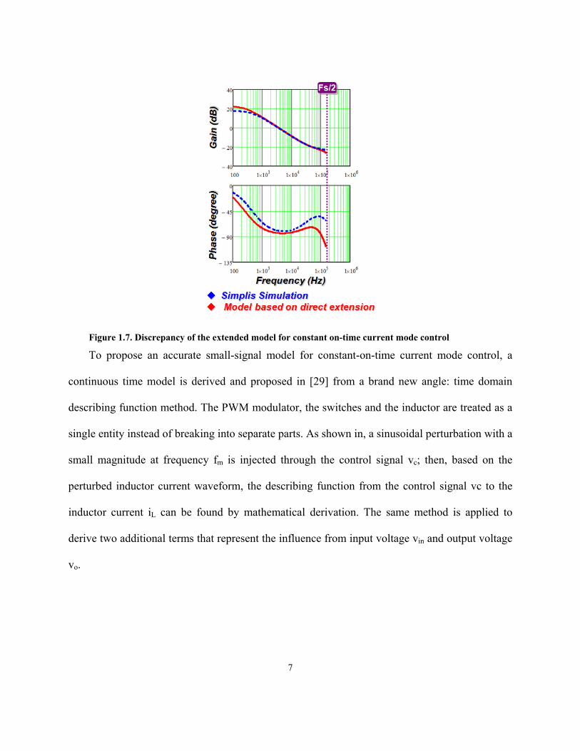
Figure 1.7. Discrepancy of the extended model for constant on-time current mode control ........................ 7
Figure 1.8. Perturbed waveform in constant on-time control. ...................................................................... 8
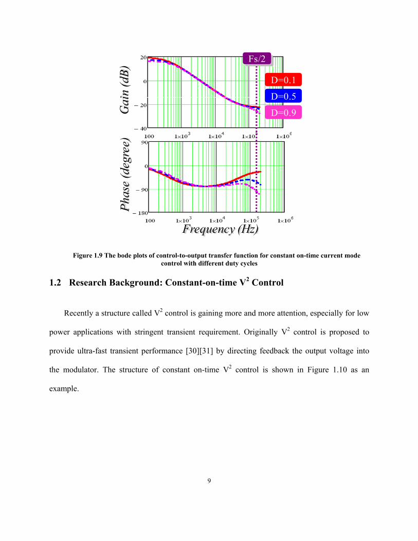
Figure 1.9 The bode plots of control-to-output transfer function for constant on-time current mode control
with different duty cycles .............................................................................................................................. 9
Figure 1.10 Structure of constant on-time V2 control ................................................................................. 10
Figure 1.11. Feedback output voltage waveform of V2 control. ................................................................. 12
Figure 1.12 Comparisons of waveforms for constant on-time V2 control with different caps when
Fsw=300kHz; D=0.1; (a) OSCON Cap (560uF/6mΩ) (b) Ceramic Cap (100uF/1.4 mΩ) .......................... 13
Figure 1.13 Extension of R. Ridley’s model to constant on-time V2 control.............................................. 14
Figure 1.14 Modeling concept for constant on-time V2 control based on describing function method ...... 16
Figure 1.15 Control to output transfer function comparison: (a) output capacitor (560μF/6mΩ), (b) output
capacitor (56μF/6mΩ). Red solid curve: Model; Blue dashed curve: Simplis simulation.......................... 17
Figure 2.1. Constant-on-time V2 control with external ramp compensation. ............................................. 23
Figure 2.2. Bode plots comparison of control-to-output transfer function between simplified small-signal
model and simplis simulation. Red solid curve: Model; Blue dashed curve: Simplis simulation .............. 25

xi
Figure 2.3 The pole-zero maps of control-to-output with two different external ramps using numerical
solutions. ..................................................................................................................................................... 26
Figure 2.4. Pole-zero map of the control-to-output transfer function with increasing se in region I .......... 31
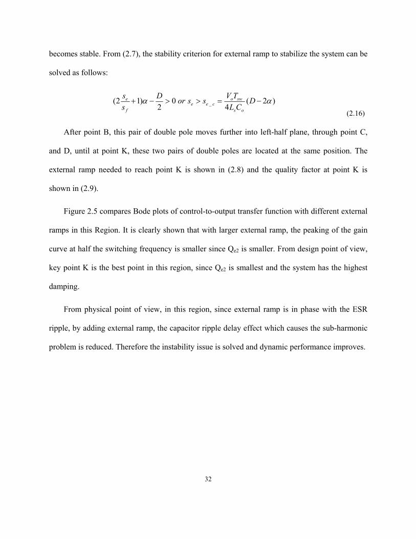
Figure 2.5. Bode plots comparison of control-to-output transfer function in region I ................................ 33
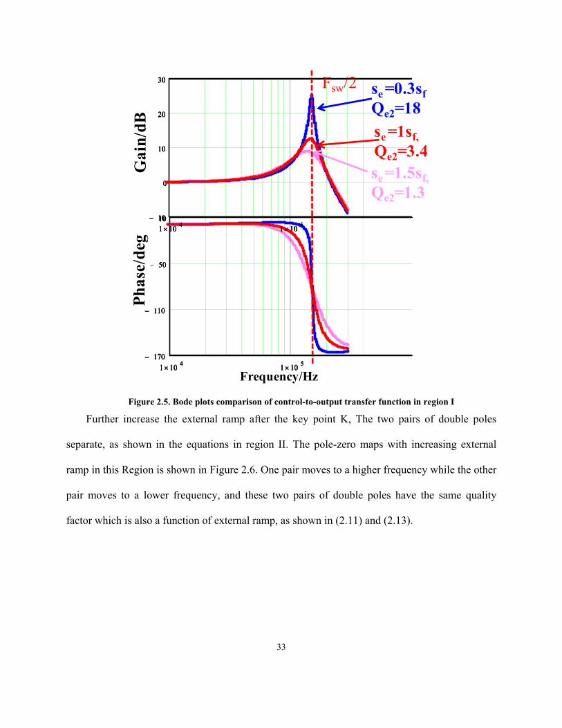
Figure 2.6. Pole-zero map of the control-to-output transfer function with increasing se in region II. ........ 34
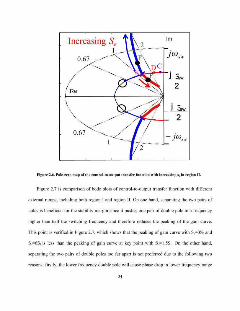
Figure 2.7. Bode plots comparison of control-to-output transfer function in region I and II. .................... 35
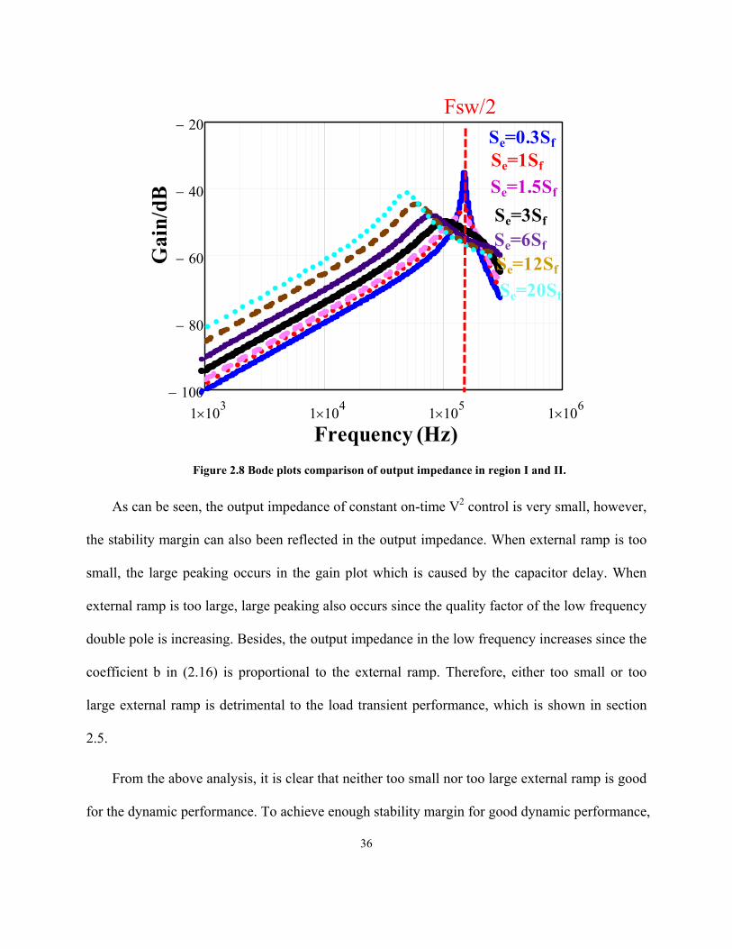
Figure 2.8 Bode plots comparison of output impedance in region I and II. ................................................ 36
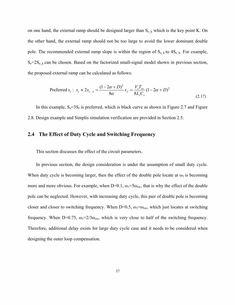
Figure 2.9. The relations between Qe_k and D with Fsw=300kHz. ............................................................... 39
Figure 2.10 Bode plots comparisons of control-to-output transfer function with different Se for D=0.1, 0.5
and 0.9 ......................................................................................................................................................... 40
Figure 2.11 Bode plots comparisons of output impedance with different Se between D=0.1, 0.5 and 0.9 . 40
Figure 2.12 The relations between Qe_k and D with Fsw=300kHz, 800kHz and 3MHz. .............................. 42
Figure 2.13 Bode plots comparison of control-to-output transfer function with different switching
frequencies. ................................................................................................................................................. 43
Figure 2.14 Comparison of control-to-output transfer function with three external ramp designs ............. 45
Figure 2.15. Bode Plots comparison of output impedance with three external ramp designs .................... 46
Figure 2.16. Load transient simplis simulations with three external ramp designs .................................... 46
Figure 2.17. Bode plots of control-to-output transfer function between model and simulation for different
duty cycles. ................................................................................................................................................. 47
Figure 2.18. Bode plots of control-to-output transfer function between model and simulation for different
switching frequencies at D=0.9 case. .......................................................................................................... 48
Figure 2.19 Constant-on-time V2 control with current ramp compensation. (a) Circuit diagram; (b)
Steady-state waveforms. ............................................................................................................................. 50
Figure 2.20. Comparison of of control-to-output transfer function with three current ramp designs (a)
Pole-zero maps (b) Bode plots. .................................................................................................................. 52
xii
Figure 2.21. Bode plots comparison of output impedance with three current ramp designs ...................... 53
Figure 2.22. Load transient simulations with three different current ramp designs .................................... 54
Figure 3.1 Circuit diagram of digital constant on-time V2 control with external ramp compensation. ...... 57
Figure 3.2 The steady-state waveform for digital constant-on-time V2 control. ......................................... 57
Figure 3.3. Pole-zero map of the control-to-output transfer function with increasing se ............................ 63
Figure 3.4 Bode plots comparison of control-to-output transfer function with different Se. ...................... 65
Figure 3.5. Bode plots comparison of output impedance with different digital external ramp. .................. 66
Figure 3.6. Bode plots comparison of control-to-output transfer function between analog and digital case
.................................................................................................................................................................... 68
Figure 3.7. Bode plots comparison of output impedance between analog and digital case ........................ 69
Figure 3.8. Control-to-output transfer function comparison of three external ramp designs of digital
constant-on-time V2 control (a) Pole-zero map. (b) Bode plots. ................................................................. 70
Figure 3.9. The output impedance comparison of three external ramp designs. ......................................... 71
Figure 3.10. FPGA-based hardware platform for digital constant-on-time V2 control. .............................. 73
Figure 3.11. Small-signal control-to-output transfer function measurement circuit. .................................. 74
Figure 3.12. Measurement results of control-to-output transfer function with different external ramps. ... 75
Figure 3.13. Comparison of small-signal model and measurement result for Se=15Sf case. ..................... 76
Figure 3.14. Load transient experimental results with three different external ramp designs for digital
constant-on-time V2 control. ....................................................................................................................... 77
1
Chapter 1. Introduction
1.1 Review of Constant-on-time Current Mode Control
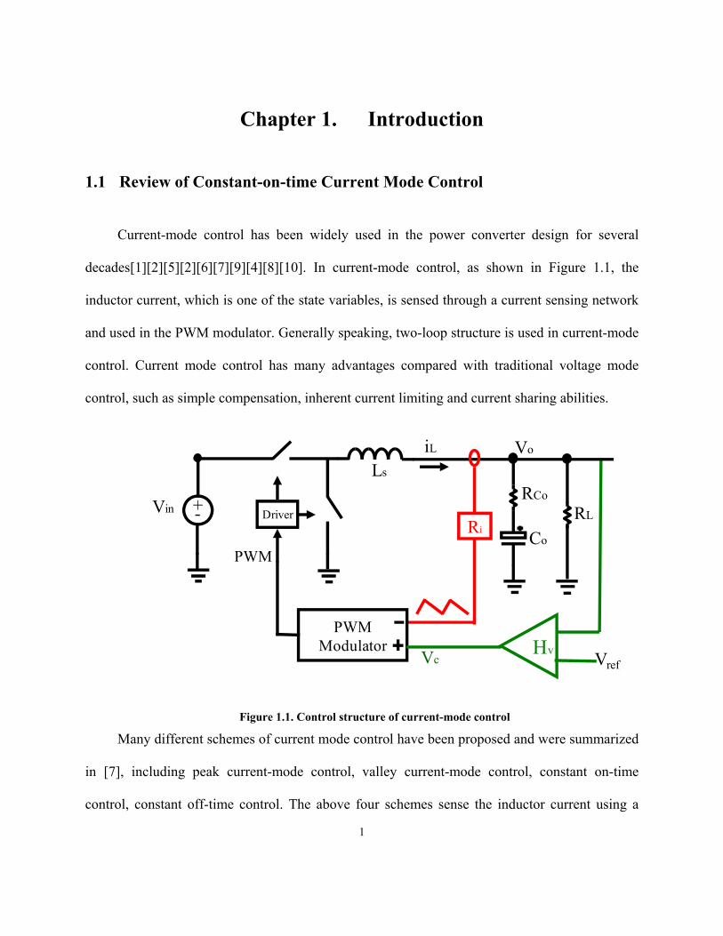
Current-mode control has been widely used in the power converter design for several
decades[1][2][5][2][6][7][9][4][8][10]. In current-mode control, as shown in Figure 1.1, the
inductor current, which is one of the state variables, is sensed through a current sensing network
and used in the PWM modulator. Generally speaking, two-loop structure is used in current-mode
control. Current mode control has many advantages compared with traditional voltage mode
control, such as simple compensation, inherent current limiting and current sharing abilities.
Figure 1.1. Control structure of current-mode control
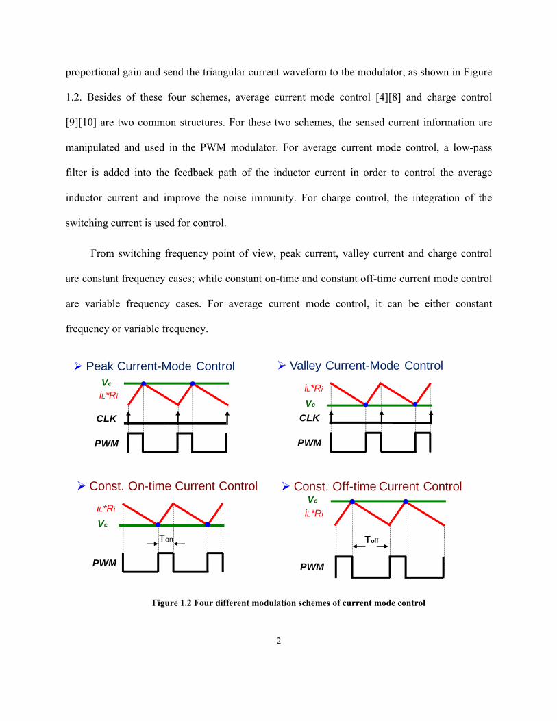
Many different schemes of current mode control have been proposed and were summarized
in [7], including peak current-mode control, valley current-mode control, constant on-time
control, constant off-time control. The above four schemes sense the inductor current using a
VrefHv
PWM
Vin
Vo
Driver
iL
RCo
Co
RL
Ls
+-Ri
PWMModulator
Vc
2
proportional gain and send the triangular current waveform to the modulator, as shown in Figure
1.2. Besides of these four schemes, average current mode control [4][8] and charge control
[9][10] are two common structures. For these two schemes, the sensed current information are
manipulated and used in the PWM modulator. For average current mode control, a low-pass
filter is added into the feedback path of the inductor current in order to control the average
inductor current and improve the noise immunity. For charge control, the integration of the
switching current is used for control.
From switching frequency point of view, peak current, valley current and charge control
are constant frequency cases; while constant on-time and constant off-time current mode control
are variable frequency cases. For average current mode control, it can be either constant
frequency or variable frequency.
Figure 1.2 Four different modulation schemes of current mode control
Const. On-time Current Control
iL*Ri
Vc
PWM
Ton
iL*Ri
Vc
PWM
CLK
Valley Current-Mode Control
iL*Ri
Vc
PWM
Toff
Const. Off-time Current Control
Peak Current-Mode Control
iL*Ri
Vc
PWM
CLK
3
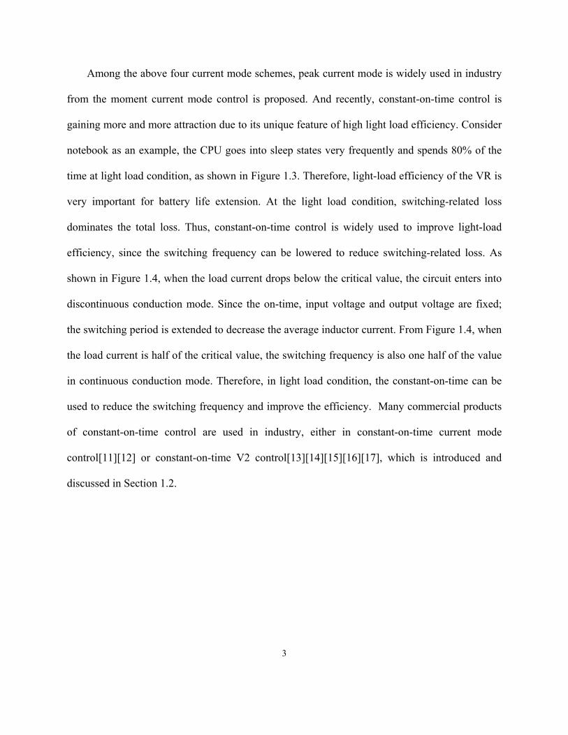
Among the above four current mode schemes, peak current mode is widely used in industry
from the moment current mode control is proposed. And recently, constant-on-time control is
gaining more and more attraction due to its unique feature of high light load efficiency. Consider
notebook as an example, the CPU goes into sleep states very frequently and spends 80% of the
time at light load condition, as shown in Figure 1.3. Therefore, light-load efficiency of the VR is
very important for battery life extension. At the light load condition, switching-related loss
dominates the total loss. Thus, constant-on-time control is widely used to improve light-load
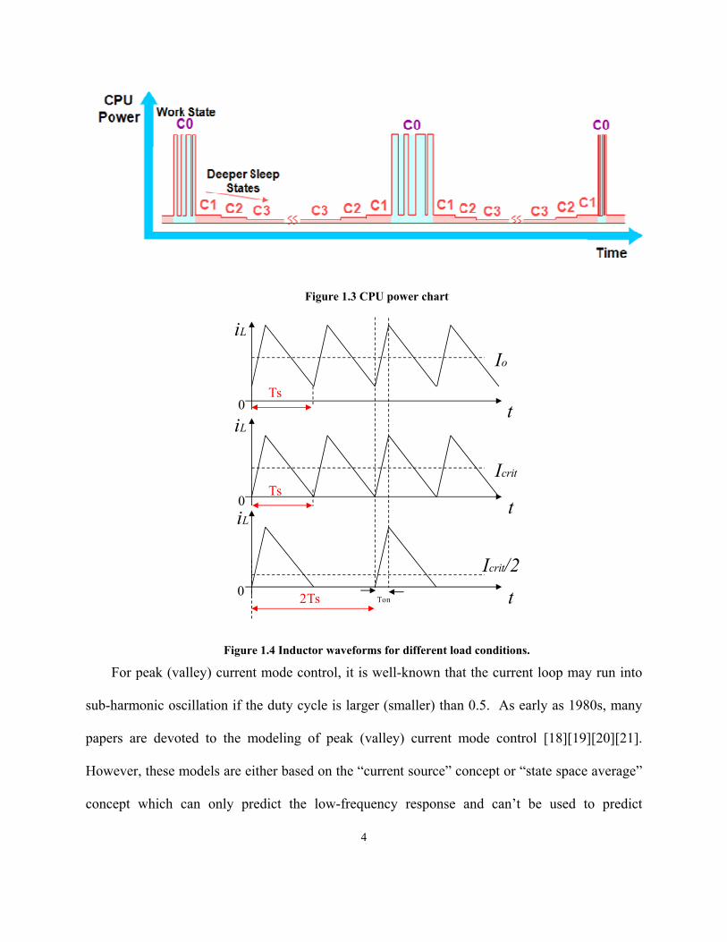
efficiency, since the switching frequency can be lowered to reduce switching-related loss. As
shown in Figure 1.4, when the load current drops below the critical value, the circuit enters into
discontinuous conduction mode. Since the on-time, input voltage and output voltage are fixed;
the switching period is extended to decrease the average inductor current. From Figure 1.4, when
the load current is half of the critical value, the switching frequency is also one half of the value
in continuous conduction mode. Therefore, in light load condition, the constant-on-time can be
used to reduce the switching frequency and improve the efficiency. Many commercial products
of constant-on-time control are used in industry, either in constant-on-time current mode
control[11][12] or constant-on-time V2 control[13][14][15][16][17], which is introduced and
discussed in Section 1.2.
4
Figure 1.3 CPU power chart
Figure 1.4 Inductor waveforms for different load conditions.
For peak (valley) current mode control, it is well-known that the current loop may run into
sub-harmonic oscillation if the duty cycle is larger (smaller) than 0.5. As early as 1980s, many
papers are devoted to the modeling of peak (valley) current mode control [18][19][20][21].
However, these models are either based on the “current source” concept or “state space average”
concept which can only predict the low-frequency response and can’t be used to predict
iL
t
Icrit/20
Ton2Ts
iL
t
Icrit
0Ts
iL
t
Io
0Ts
5
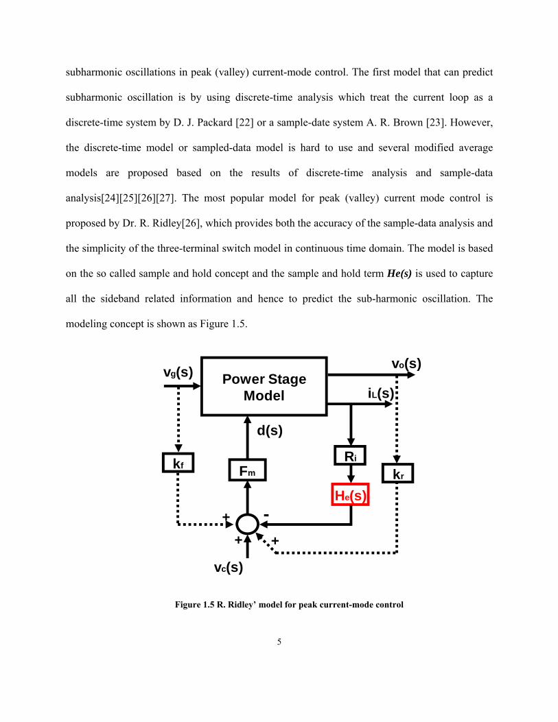
subharmonic oscillations in peak (valley) current-mode control. The first model that can predict
subharmonic oscillation is by using discrete-time analysis which treat the current loop as a
discrete-time system by D. J. Packard [22] or a sample-date system A. R. Brown [23]. However,
the discrete-time model or sampled-data model is hard to use and several modified average
models are proposed based on the results of discrete-time analysis and sample-data
analysis[24][25][26][27]. The most popular model for peak (valley) current mode control is
proposed by Dr. R. Ridley[26], which provides both the accuracy of the sample-data analysis and
the simplicity of the three-terminal switch model in continuous time domain. The model is based
on the so called sample and hold concept and the sample and hold term He(s) is used to capture
all the sideband related information and hence to predict the sub-harmonic oscillation. The
modeling concept is shown as Figure 1.5.
Figure 1.5 R. Ridley’ model for peak current-mode control
kr
+
Ri
He(s)
Fm
vc(s)
Power StageModel
vo(s)
iL(s)
d(s)
vg(s)
-+
kf
+
6
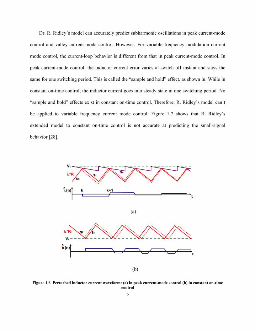
Dr. R. Ridley’s model can accurately predict subharmonic oscillations in peak current-mode
control and valley current-mode control. However, For variable frequency modulation current
mode control, the current-loop behavior is different from that in peak current-mode control. In
peak current-mode control, the inductor current error varies at switch off instant and stays the
same for one switching period. This is called the “sample and hold” effect. as shown in. While in
constant on-time control, the inductor current goes into steady state in one switching period. No
“sample and hold” effects exist in constant on-time control. Therefore, R. Ridley’s model can’t
be applied to variable frequency current mode control. Figure 1.7 shows that R. Ridley’s
extended model to constant on-time control is not accurate at predicting the small-signal
behavior [28].
(a)
(b)
Figure 1.6 Perturbed inductor current waveform: (a) in peak current-mode control (b) in constant on-time control
7
Figure 1.7. Discrepancy of the extended model for constant on-time current mode control
To propose an accurate small-signal model for constant-on-time current mode control, a
continuous time model is derived and proposed in [29] from a brand new angle: time domain
describing function method. The PWM modulator, the switches and the inductor are treated as a
single entity instead of breaking into separate parts. As shown in, a sinusoidal perturbation with a
small magnitude at frequency fm is injected through the control signal vc; then, based on the
perturbed inductor current waveform, the describing function from the control signal vc to the
inductor current iL can be found by mathematical derivation. The same method is applied to
derive two additional terms that represent the influence from input voltage vin and output voltage
vo.

8
Figure 1.8. Perturbed waveform in constant on-time control.
Essentially, the current mode control converter is an infinite order system. For practical
design purposes, the system can be simplified as a third order system.The simplified control-to-
Vo transfer function for constant-on-time current mode control is shown as follows:
21
2
11
1
1
1/
1
)(
)(
s
Q
ss
sCRK
sv
sv
a
oCoc
c
o
(1.1)
Where ω1=π/Ton, Q1=2/π. From ((1.1), the location of double poles is determined by Ton and
the quality factor is always positive which means that the double poles never move to the right
half plane. From the bode plots shown in Figure 1.9, for constant on-time current mode control,
the current loop is always stable and no sub-harmonic oscillation occurs.
TonToffPWM
r0Sf
Sn
t1=0 t2 t3 ti
TonToff(1) Toff(2)PWM’ Toff(i)
tM
Toff(M)
vc (t)
9
Figure 1.9 The bode plots of control-to-output transfer function for constant on-time current mode control with different duty cycles
1.2 Research Background: Constant-on-time V2 Control
Recently a structure called V2 control is gaining more and more attention, especially for low
power applications with stringent transient requirement. Originally V2 control is proposed to
provide ultra-fast transient performance [30][31] by directing feedback the output voltage into
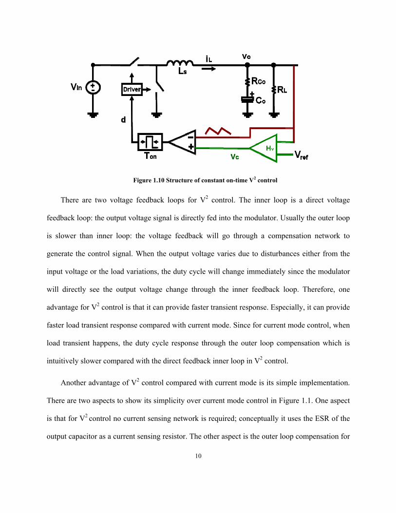
the modulator. The structure of constant on-time V2 control is shown in Figure 1.10 as an
example.
D=0.1
D=0.5
D=0.9
Fs/2
Pha
se (d
egre
e)G
ain
(dB
)
Frequency (Hz)
10
Figure 1.10 Structure of constant on-time V2 control
There are two voltage feedback loops for V2 control. The inner loop is a direct voltage
feedback loop: the output voltage signal is directly fed into the modulator. Usually the outer loop
is slower than inner loop: the voltage feedback will go through a compensation network to
generate the control signal. When the output voltage varies due to disturbances either from the
input voltage or the load variations, the duty cycle will change immediately since the modulator
will directly see the output voltage change through the inner feedback loop. Therefore, one
advantage for V2 control is that it can provide faster transient response. Especially, it can provide
faster load transient response compared with current mode. Since for current mode control, when
load transient happens, the duty cycle response through the outer loop compensation which is
intuitively slower compared with the direct feedback inner loop in V2 control.
Another advantage of V2 control compared with current mode is its simple implementation.
There are two aspects to show its simplicity over current mode control in Figure 1.1. One aspect
is that for V2 control no current sensing network is required; conceptually it uses the ESR of the
output capacitor as a current sensing resistor. The other aspect is the outer loop compensation for
11
V2 control is simpler than current mode control. In current mode control, the outer loop
bandwidth is responsible for the load transient performance and typically a one-zero two-pole
compensation network (or type II compensation) is required to achieve the desired bandwidth
and stability margin. In V2 control, a low-bandwidth integrator network is enough since the
purpose of the outer loop is to eliminate the steady state error which equals to half of the output
voltage switching ripple instead of its responsibility for the transient performance. In some
applications which does not care so much about the steady state error, even no outer loop is used,
which is referred as ripple based control in some literatures[32][33].
V2 control can be implemented as constant frequency modulation (including constant
frequency V2 peak control or constant frequency V2 valley control) or variable frequency
modulation (including constant on-time V2 control and constant off-time V2 control). Constant
on-time V2 control is the most widely used in industry [13][14][15][16][17], as compared with
other V2 control structures, high light load efficiency can be achieved by employing constant on-
time control.
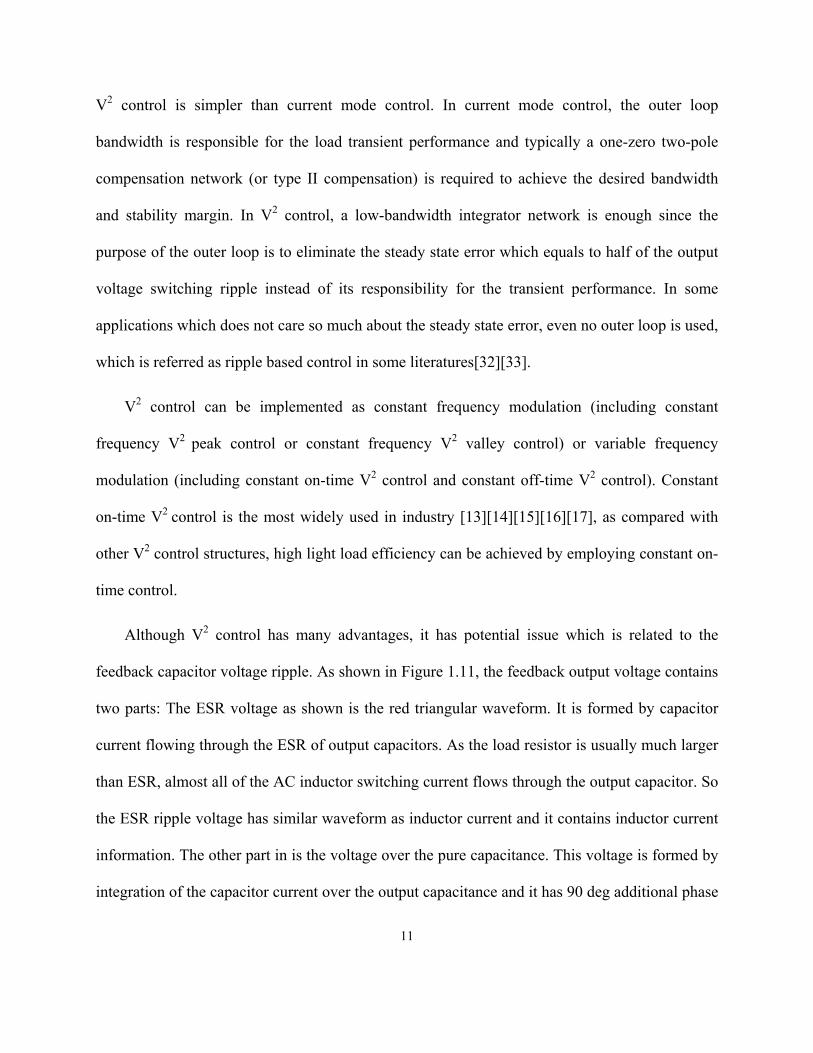
Although V2 control has many advantages, it has potential issue which is related to the
feedback capacitor voltage ripple. As shown in Figure 1.11, the feedback output voltage contains
two parts: The ESR voltage as shown is the red triangular waveform. It is formed by capacitor
current flowing through the ESR of output capacitors. As the load resistor is usually much larger
than ESR, almost all of the AC inductor switching current flows through the output capacitor. So
the ESR ripple voltage has similar waveform as inductor current and it contains inductor current
information. The other part in is the voltage over the pure capacitance. This voltage is formed by
integration of the capacitor current over the output capacitance and it has 90 deg additional phase
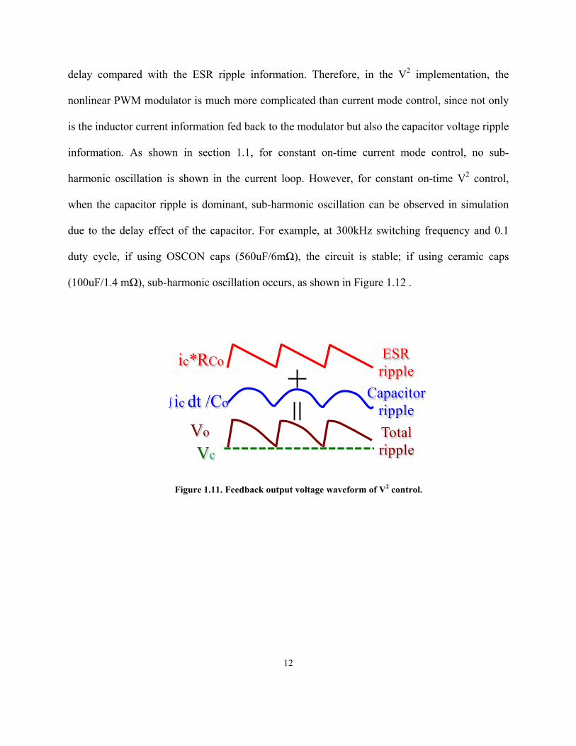
12
delay compared with the ESR ripple information. Therefore, in the V2 implementation, the
nonlinear PWM modulator is much more complicated than current mode control, since not only
is the inductor current information fed back to the modulator but also the capacitor voltage ripple
information. As shown in section 1.1, for constant on-time current mode control, no sub-
harmonic oscillation is shown in the current loop. However, for constant on-time V2 control,
when the capacitor ripple is dominant, sub-harmonic oscillation can be observed in simulation
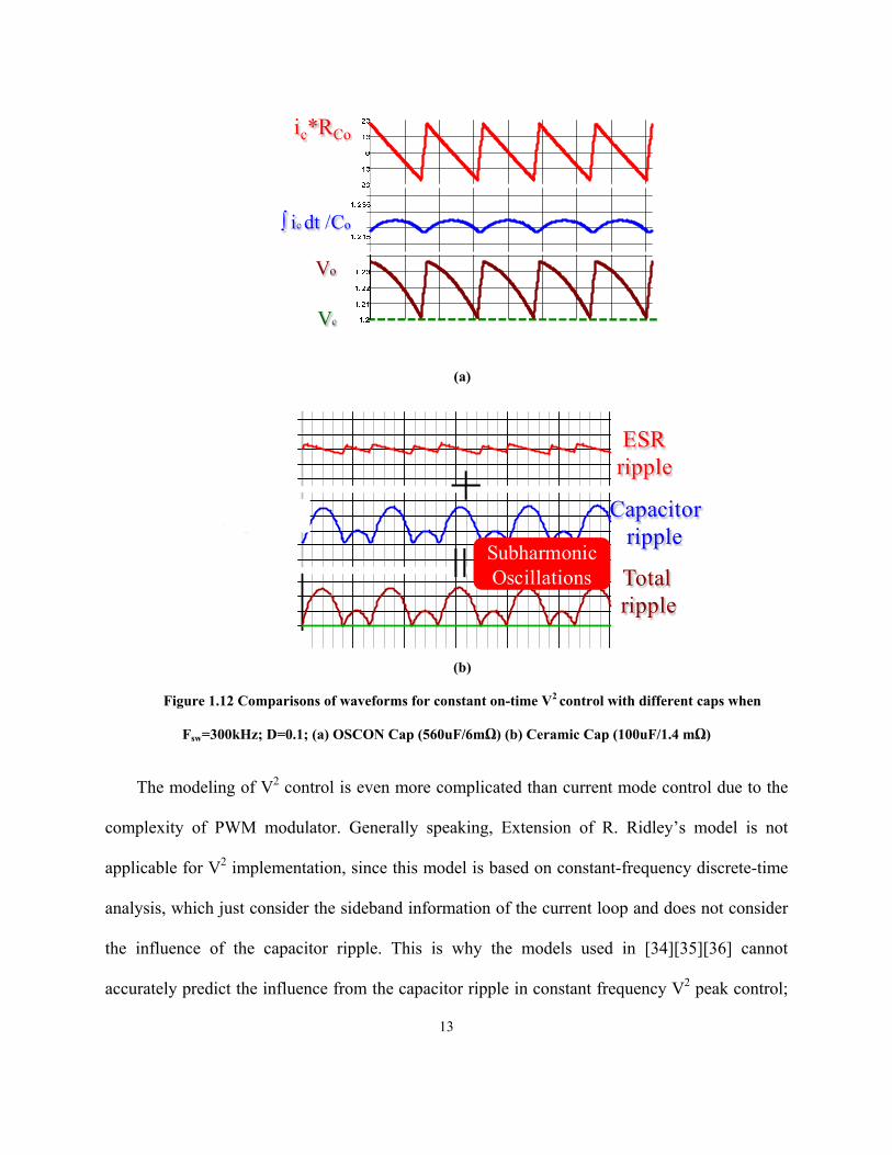
due to the delay effect of the capacitor. For example, at 300kHz switching frequency and 0.1
duty cycle, if using OSCON caps (560uF/6mΩ), the circuit is stable; if using ceramic caps
(100uF/1.4 mΩ), sub-harmonic oscillation occurs, as shown in Figure 1.12 .
Figure 1.11. Feedback output voltage waveform of V2 control.
ic*RCo ESRripple
∫ ic dt /CoCapacitor
ripple
Vo
Vc
Totalripple
+=
13
(a)
(b)
Figure 1.12 Comparisons of waveforms for constant on-time V2 control with different caps when
Fsw=300kHz; D=0.1; (a) OSCON Cap (560uF/6mΩ) (b) Ceramic Cap (100uF/1.4 mΩ)
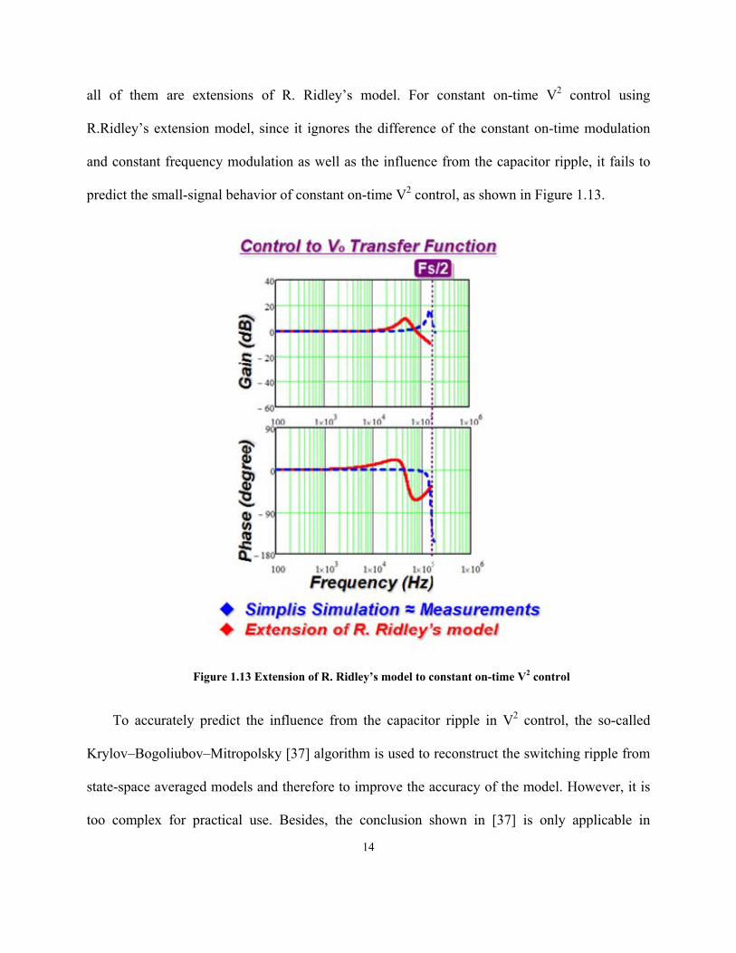
The modeling of V2 control is even more complicated than current mode control due to the
complexity of PWM modulator. Generally speaking, Extension of R. Ridley’s model is not
applicable for V2 implementation, since this model is based on constant-frequency discrete-time
analysis, which just consider the sideband information of the current loop and does not consider
the influence of the capacitor ripple. This is why the models used in [34][35][36] cannot
accurately predict the influence from the capacitor ripple in constant frequency V2 peak control;
∫ ic dt /Co
Vo
Vc
ic*RCo
Capacitorripple
∫ ic dt /Co
ESRripple
Total ripple
+=
SubharmonicOscillations
14
all of them are extensions of R. Ridley’s model. For constant on-time V2 control using
R.Ridley’s extension model, since it ignores the difference of the constant on-time modulation
and constant frequency modulation as well as the influence from the capacitor ripple, it fails to
predict the small-signal behavior of constant on-time V2 control, as shown in Figure 1.13.
Figure 1.13 Extension of R. Ridley’s model to constant on-time V2 control
To accurately predict the influence from the capacitor ripple in V2 control, the so-called
Krylov–Bogoliubov–Mitropolsky [37] algorithm is used to reconstruct the switching ripple from
state-space averaged models and therefore to improve the accuracy of the model. However, it is
too complex for practical use. Besides, the conclusion shown in [37] is only applicable in
15
constant frequency V2 control and no small-signal model and design analysis is presented for
constant-on-time V2 control. In [38], the sampled-data modeling technique which is based on the
response of inductor current and capacitor voltage at the switching instants is used to derive the
stability criterion for V2 control based on the sign of the Eigen values of the state transition
matrix. Although the stability criterion can be derived using this method, this method is based on
the discrete-time analysis and is not easy to use since most of power electronics engineers are
costumed to continuous time analysis. Besides, no continuous-time transfer function is provided
and no stability margin can be controlled for design purpose.
Recently V2 control is modeled based on describing function method by Dr. Jian Li [39],
which is an extension of the modeling work for current mode control, as shown in Section 1.1. In
order to capture the nonlinearity of the circuit, the power stage as well as the inner voltage
feedback is considered as a single entity. By doing this, the influence from capacitor voltage
ripple is considered and included in the modeling result. The modeling concept is shown as in
Figure 1.14. A small-signal sinusoidal perturbation is injected into the control signal, and the
time domain output voltage variation is calculated. After the time domain relation between
control signal perturbation and output voltage variation is obtained, the time domain relation is
transferred into frequency domain using Fourier analysis.
16
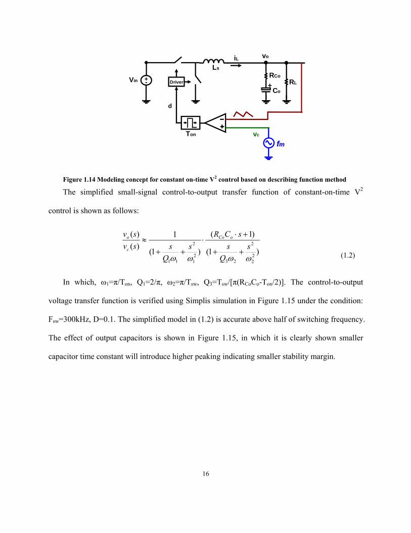
Figure 1.14 Modeling concept for constant on-time V2 control based on describing function method
The simplified small-signal control-to-output transfer function of constant-on-time V2
control is shown as follows:
)1(
)1(
)1(
1
)(
)(
22
2
2321
2
11 s
Q
s
sCR
s
Q
ssv
sv oCo
c
o
(1.2)
In which, ω1=π/Ton, Q1=2/π, ω2=π/Tsw, Q3=Tsw/[π(RCoCo-Ton/2)]. The control-to-output
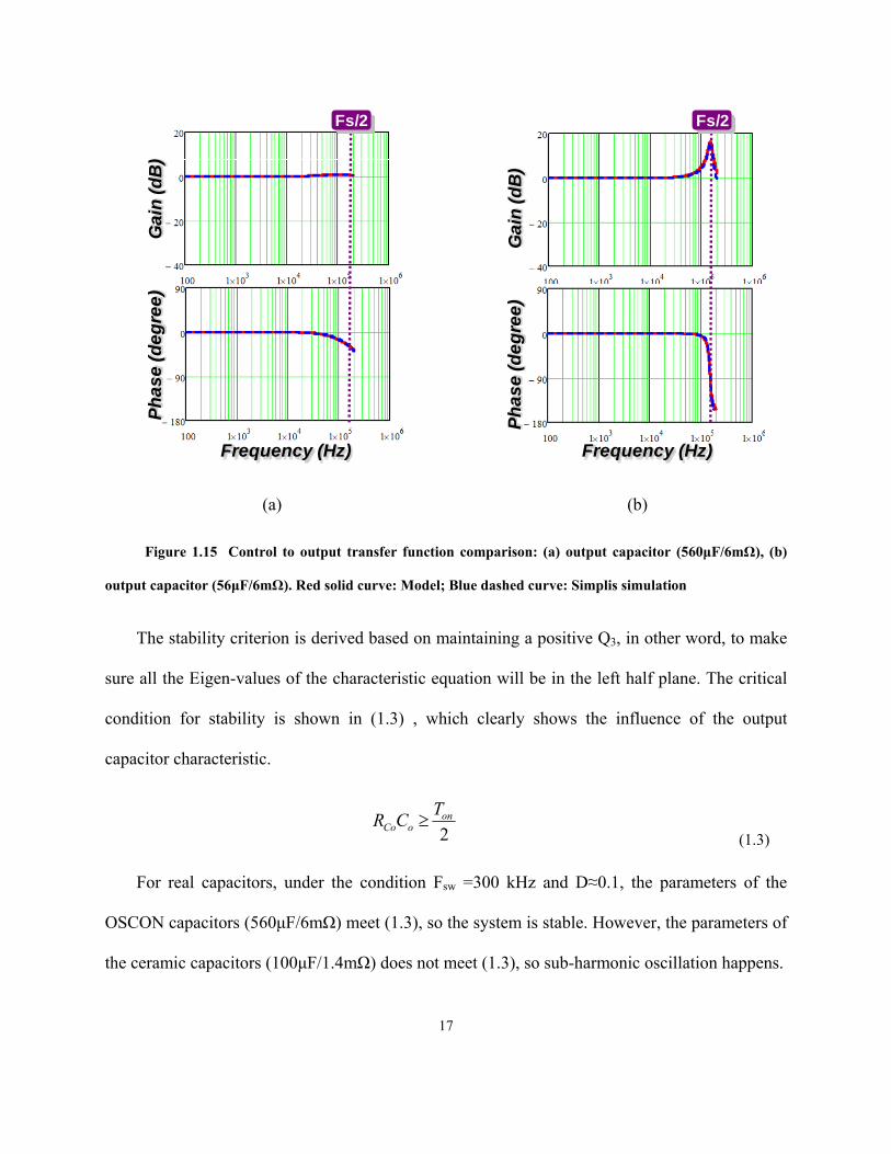
voltage transfer function is verified using Simplis simulation in Figure 1.15 under the condition:
Fsw=300kHz, D=0.1. The simplified model in (1.2) is accurate above half of switching frequency.
The effect of output capacitors is shown in Figure 1.15, in which it is clearly shown smaller
capacitor time constant will introduce higher peaking indicating smaller stability margin.
fm
d
Vin
vo
Driver
iL
RCo
Co
RL
Ls
+- +
Ton vc
17
(a) (b)
Figure 1.15 Control to output transfer function comparison: (a) output capacitor (560μF/6mΩ), (b)
output capacitor (56μF/6mΩ). Red solid curve: Model; Blue dashed curve: Simplis simulation
The stability criterion is derived based on maintaining a positive Q3, in other word, to make
sure all the Eigen-values of the characteristic equation will be in the left half plane. The critical
condition for stability is shown in (1.3) , which clearly shows the influence of the output
capacitor characteristic.
2on
oCo
TCR
(1.3)
For real capacitors, under the condition Fsw =300 kHz and D≈0.1, the parameters of the
OSCON capacitors (560μF/6mΩ) meet (1.3), so the system is stable. However, the parameters of
the ceramic capacitors (100μF/1.4mΩ) does not meet (1.3), so sub-harmonic oscillation happens.
Fs/2
Ph
as
e (
de
gre
e)
Ga
in (
dB
)
Frequency (Hz)
Fs/2
Ph
as
e (
de
gre
e)
Ga
in (
dB
)
Frequency (Hz)
18
However, in many applications such as digital camera, netbook, cellular phone, ceramic
caps are preferred due to its small size and small output voltage ripple requirement. Two
solutions to eliminate sub-harmonic oscillations are discussed in [39] and the small-signal
models are also derived based on time-domain describing function. One method is by adding an
external ramp and the other is by adding the current ramp. However, the characteristic of
constant-on-time V2 with external ramp is not fully understood since the control to output
transfer function in [39] is not factorized and the numerical solution is used instead of identifying
the pole-zero movements. As a result, no explicit design guideline for the external ramp is
provided and the influence of the circuit parameters is not clear either. Therefore, one primary
objective of this thesis is to gain better understanding of the characteristic for constant-on-time
V2 with external ramp by identifying the pole-zero movements based on the factorized small-
signal model, as well as to provide an analytical solution of the external ramp design for constant
on-time V2 control and investigating the influence of the circuit parameters.
Recently, digital control techniques have become more and more popular for many DC/DC
switching converters due to its unique capabilities such as re-programmability, better noise
immunity, etc [40]. The traditional digital voltage mode architecture evolved directly from
analog voltage mode. The difference between the digital structure and the analog structure is that
two major quantizers, the analog-to-digital converter (ADC) and the digital pulse-width
modulator (DPWM), are added into the digital system. Unfortunately, unpredicted limit-cycle
oscillation may occur due to the quantization effects of those two quantizers[41]. High-resolution
DPWM is indispensable for minimizing the possibility of the limit-cycle oscillation [41][42].
However, the DPWM with high resolution is expensive and introduces more challenges to the
19
digital controller design. A digital constant-on-time V2 structure with external ramp is proposed
in [43] to reduce the limit cycle oscillation amplitude and therefore reduce the design challenge
for the digital control IC by getting rid of the high resolution PWM. The small-signal model of
the proposed digital constant-on-time V2 structure is presented in [44] and it is shown that the
selection of the external ramp is not only related to the amplitude of the limit-cycle oscillation,
but also to the stability of the system. The detailed characteristic of the digital constant-on-time
V2 control with external ramps is analyzed in [45]. However, the analysis is not thorough since
numerical solution is used and no analytical form of stability criterion and design guideline is
provided. Besides, it is meaningful to provide experimental verification of the small-signal
analysis since the assumptions which are made when deriving the small-signal models in [44][45]
need to be justified experimentally. Therefore, another objective of this thesis is to gain better
understanding of the characteristic for digital constant-on-time V2 with external ramp to provide
the external ramp design guideline and investigating the influence of sampling effect as well as
to provide small-signal experimental results for digital constant-on-time V2 control.
1.3 Thesis Outline
Constant-on-time V2 control architecture has been widely applied in DC-DC buck
converters mainly due to the following three features: 1) simple control architecture with a
simpler outer-loop compensator and without current sensing resistor 2) fast load transient
characteristics with direct output voltage feedback and 3) good light-load efficiency with
20
constant-on-time structure. However, for the converters with low-ESR capacitors such as
ceramic caps, the conventional V2 control suffers from the sub-harmonic oscillation due to the
lagging phase of the capacitor voltage ripple relative to the inductor current ripple. Two solutions
to eliminate sub-harmonic oscillations are discussed in [39] and the small-signal models are also
derived based on time-domain describing function. However, the characteristic of constant-on-
time V2 with external ramp is not fully understood and no explicit design guideline for the
external ramp is provided. For digital constant on-time V2 control, the high resolution PWM can
be eliminated due to constant on-time modulation scheme and direct output voltage feedback.
However, the external ramp design is not only related to the amplitude of the limit-cycle
oscillation, but also very important to the stability of the system. The previous analysis is not
through since numerical solution is used. The primary objective of this work is to gain better
understanding of the small-signal characteristic for analog and digital constant-on-time V2 with
ramp compensations, and provide the design guideline based on the factorized small-signal
model.
The detailed outline is elaborated as follows.
Chapter 1 is the review of the background of constant on-time current-mode control and
constant on-time V2 control. For applications with ceramic caps, the conventional V2 control
suffers from the sub-harmonic oscillation due to the lagging phase of the capacitor voltage
ripple. Two solutions are previously proposed to solve the sub-harmonic oscillation. However,
the characteristic of constant-on-time V2 with external ramp is not fully understood. The primary
objective of this thesis is to gain better understanding of the characteristic for analog and digital
21
constant-on-time V2 and provide the design guideline by identifying the pole-zero movements
based on the factorized small-signal model.
In Chapter 2, the small-signal model and design of analog constant on-time V2 control is
discussed. The small-signal models are factorized and pole-zero movements are identified. Two
regions with different small-signal characteristics are presented based on the magnitude of
external ramps. After that, the stability criterion and design guideline of the external ramp are
provided to achieve good dynamic performances. The effect of the circuit parameters is also
given and comparisons between external ramp compensation and current ramp compensation are
provided. Design examples are given to verify the analysis.
In Chapter 3, the small-signal model and design of digital constant on-time V2 control is
discussed. The factorized strategy of the small-signal model and design strategy of the external
ramp is extended also to digital constant on-time V2 control. The sampling effects are revealed
by comparison between the small-signal model of analog and digital constant on-time V2 control.
One simple method to measure the small-signal model of digital constant on-time V2 control is
presented and the experimental results verify the small signal analysis.
Chapter 4 is conclusions with the summary and the future work.
22
Chapter 2. Small-signal Analysis and Design of Analog
Constant-on-time V2 Control
As shown in previous chapter, sub-harmonic problem occurs for constant-on-time V2 control
using ceramic caps. To solve the instability problem, two solutions are presented in [39] and the
small-signal model is derived based on the describing function method. One is using external
ramp compensation and the other is using current ramp compensation. However, the
characteristic for constant-on-time V2 control with external ramp compensation is not fully
understood and there is no design guideline provided for the external ramp. Besides, the effect of
circuit parameters such as duty cycle and switching frequency is not clear due to lack of enough
understanding of the small-signal characteristic. This chapter tries to gain a better understanding
of the characteristic for constant-on-time V2 control with external ramp compensation by
factorizing the small-signal control-to-output transfer function. Based on that, the design
consideration for external ramp is discussed and design guideline is provided to achieve good
dynamic performance. Furthermore, the effect of the circuit parameter is also given and
comparisons between external ramp compensation and current ramp compensation are provided.
Simplis simulation is used to verify the analysis.
2.1 Previous Small-signal Model with External Ramp Compensation
Figure 2.1(a) shows the circuit diagram of analog constant-on-time V2 control with external
ramp compensation. Figure 2.1(b) illustrates the steady-state waveforms. As shown in Figure
2.1(b), the output voltage ripple is dominated by the capacitor voltage ripple, and the external
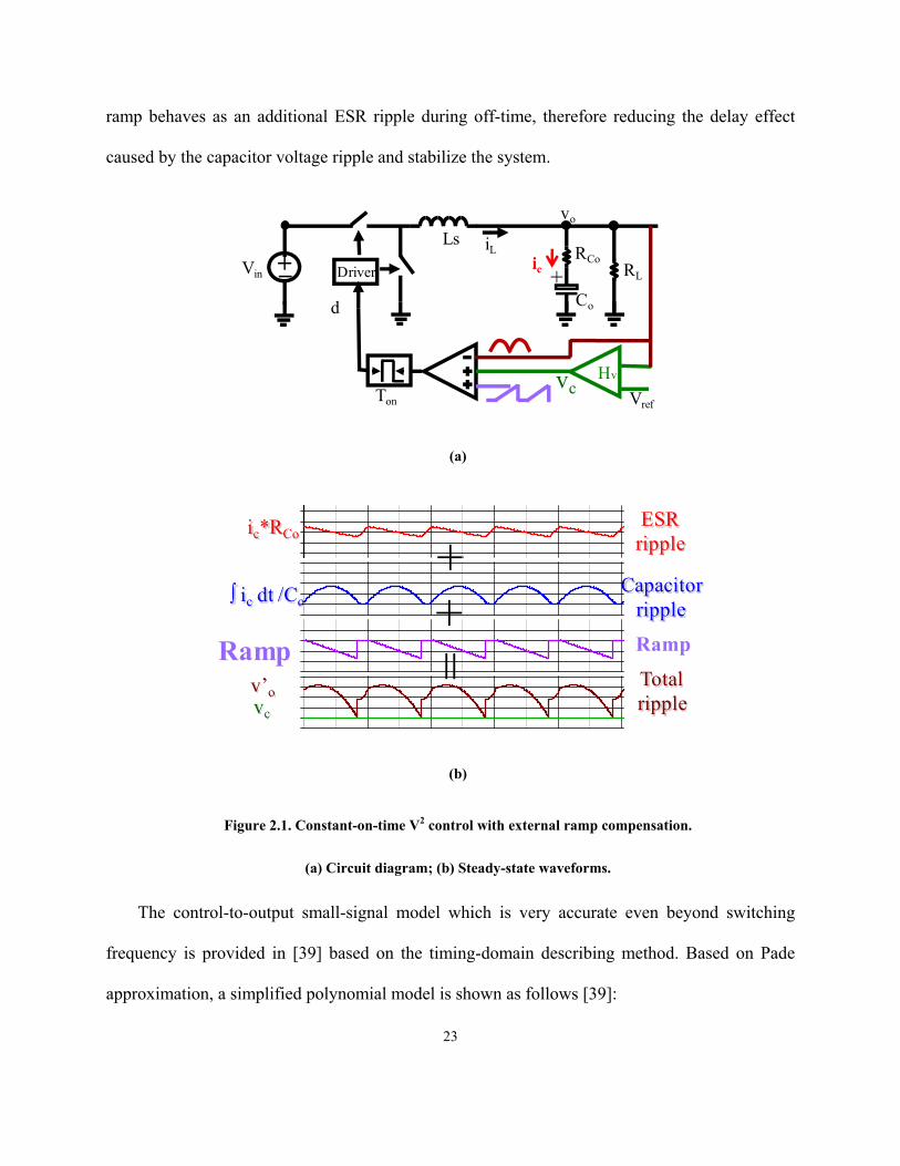
23
ramp behaves as an additional ESR ripple during off-time, therefore reducing the delay effect
caused by the capacitor voltage ripple and stabilize the system.
(a)
(b)
Figure 2.1. Constant-on-time V2 control with external ramp compensation.
(a) Circuit diagram; (b) Steady-state waveforms.
The control-to-output small-signal model which is very accurate even beyond switching
frequency is provided in [39] based on the timing-domain describing method. Based on Pade
approximation, a simplified polynomial model is shown as follows [39]:
Vin
d
vo
Driver
iL RCo
Co
RL
Ls
+_+
Ton
vcVref
Hv
ic
ic*RCo
∫ ic dt /Co
Rampv’ovc
++=
Capacitorripple
ESRripple
Totalripple
Ramp
24
222
2
2122
2
23
22
2
22
21
2
11
)1)(1(
)1)(1(
)1(
1
)(
)(
sTCRs
ss
Q
ss
Q
s
sCRs
Q
s
s
Q
ssv
sv
swoCof
e
oCo
c
o
(2.1)
where Tsw is the switching period, RCo is the ESR of the output capacitors, Co is the
capacitance of the output capacitors, ω1=π/Ton, Q1=2/π, ω2=π/Tsw, Q2=2/π, sf =RCoVo/L, L is the
inductance of the inductor, Q3=Tsw/[RCoCo-Ton/2]π, Ton is the on-time. Since ESR zero of the
output ceramic capacitor is very high compared with the switching frequency, if the duty ratio is
small, then the transfer function can be further simplified as follows:
222
2
2122
2
23
22
2
22
)1)(1(
)1(
)(
)(
sTCRs
ss
Q
ss
Q
s
s
Q
s
sv
sv
swoCof
ec
o
(2.2)
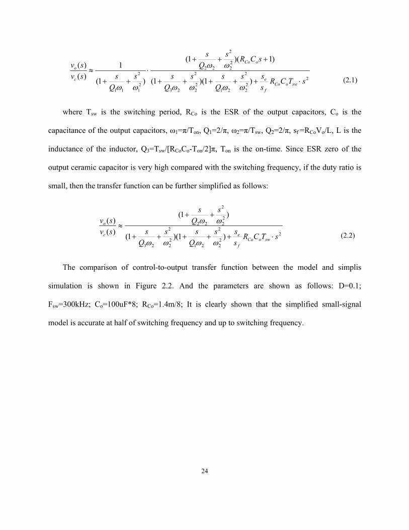
The comparison of control-to-output transfer function between the model and simplis
simulation is shown in Figure 2.2. And the parameters are shown as follows: D=0.1;
Fsw=300kHz; Co=100uF*8; RCo=1.4m/8; It is clearly shown that the simplified small-signal
model is accurate at half of switching frequency and up to switching frequency.
25
Figure 2.2. Bode plots comparison of control-to-output transfer function between simplified small-signal
model and simplis simulation. Red solid curve: Model; Blue dashed curve: Simplis simulation
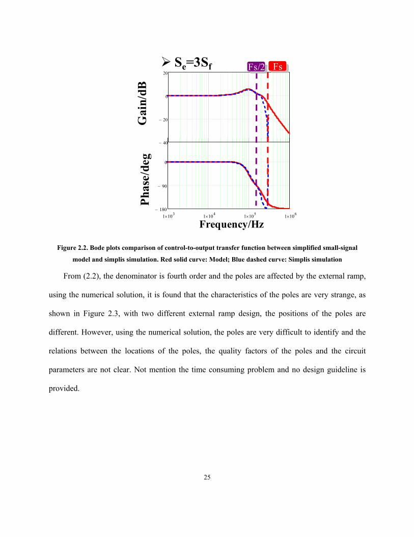
From (2.2), the denominator is fourth order and the poles are affected by the external ramp,
using the numerical solution, it is found that the characteristics of the poles are very strange, as
shown in Figure 2.3, with two different external ramp design, the positions of the poles are
different. However, using the numerical solution, the poles are very difficult to identify and the
relations between the locations of the poles, the quality factors of the poles and the circuit
parameters are not clear. Not mention the time consuming problem and no design guideline is
provided.
1 103 1 10
4 1 105 1 10
6180
90
0
40
20
0
20Fs/2 Fs Se=3Sf
Pha
se/d
egG
ain/
dB
Frequency/Hz
26
Figure 2.3 The pole-zero maps of control-to-output with two different external ramps using numerical
solutions.
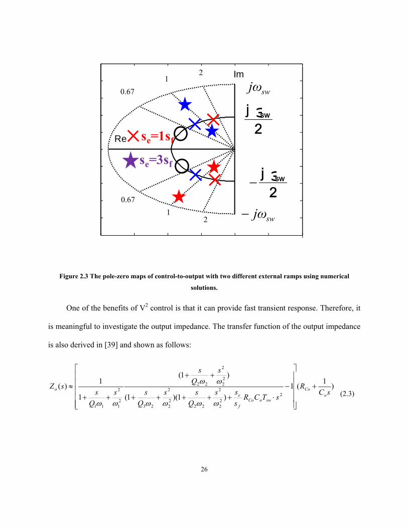
One of the benefits of V2 control is that it can provide fast transient response. Therefore, it
is meaningful to investigate the output impedance. The transfer function of the output impedance
is also derived in [39] and shown as follows:
9 . 4 2 e + 0 0 5
9 . 4 2 e + 0 0 5
0 . 7 5
0 . 5 0 . 2 5
0 . 7 5
0 . 5 0 . 2 5
21
0.67
21
0.67
Im
Re
2j ωsw
2j ωsw
swjω
swjω
se=1sf
se=3sf
)1
(1
)1)(1(
)1(
1
1)(
222
2
2222
2
23
22
2
22
21
2
11
sCR
sTCRs
ss
Q
ss
Q
s
s
Q
s
s
Q
ssZ
oCo
swoCof
eo
(2.3)
27
For the same reason, since the denominator is not factorized, the characteristic of the output
impedance is not very clear. Factorized model and pole zero identification is necessary for
analysis and design purpose.
2.2 Factorized Small-signal Model with External Ramp Compensation
To better understand the system characteristic with different external ramp and therefore
provide design guideline of the external ramp and understand the circuit parameter effect, it is
meaningful and worthwhile to identify the pole-zero movements by factorizing the fourth-order
denominator. The transfer function (2.2) can be factorized in the following form:
))/()/(
1)()()(
1(
)1(
)(
)(
22
2
222
2
2
21
22
2
22
a
s
aQ
s
a
s
aQ
s
s
Q
s
sv
sv
ee
c
o
(2.4)
where a, Qe1, Qe2 are all real numbers. The factorized results are dividing into two Regions
based on the different amplitudes of the external ramp, which are shown as follows. The
factorization details are shown in appendix A.
Region I: for relatively small external ramp.
fe sD
s
16
)21( 2
(2.5)
Where α is defined as following:
28
sw
oCo
T
CR
(2.6)
The expressions of a, Qe1 and Qe2 in (2.4) are shown as follows:
fe
e
fe
e
ssDDQ
ssDDQ
a
/16)21(21
14
/16)21(21
14
1
22
21
(2.7)
In this region, a=1 means that both pairs of double poles are located at half the switching
frequency. The external ramp changes Qe1 and Qe2, as shown in (2.7). At the key point se=se_k ,
Qe1 =Qe2=Qe_k, As shown in the following:
fKe sD
s
16
)21(:pointKey
2
_
(2.8)
DQQQ Keee
21
14:pointKey _21
(2.9)
Region II: for relatively large external ramp.
fe sD
s
16
)21( 2
(2.10)
The expression of a in (2.4) in this region is shown as follows:
12
4
YYa
(2.11)
29
22
222
2142
)12(22
12
2)12(
4D
D
s
sD
s
sY
f
e
f
e
(2.12)
The expressions of Qe1 and Qe2 in (2.4) in this region are shown as follows:
)1
(21
1221 a
aD
QQ ee
(2.13)
As external ramp increases, a>1 in (2.11) means the two pairs of double poles are separated
and are not located at half the switching frequency any more. One pair of double pole moves to a
higher frequency while the other pair of double pole moves to a lower frequency. The interesting
phenomenon is that these two pairs of double poles have the same quality factor in this region
which is shown in (2.13). Compare (2.7), (2.9) and (2.13), it is found that at the key point Qe2
reaches its minimum value, which is very important for design from the dynamic performance
point of view, which will be discussed in section 2.3.
For the output impedance, with the denominator factorized, (2.3) can be simplified and
rewritten as follows:
If the duty cycle is small and for ceramic caps, usually the output ESR zero is high
compared with switching frequency, then (2. 14) can be simplified as (2.15).
)2
(2
1
1
1
))/()/(
1)()()(
1()(
2
22
21
2
112
2
2
222
2
2
21
D
T
CRDD
C
TTR
s
sb
s
Q
s
sCR
a
s
aQ
s
a
s
aQ
ssb
sZ
sw
oCo
o
swswCo
f
e
oCo
ee
o
(2. 14)
30
From (2.15), the output impedance of constant on-time V2 control has a zero at origin, and
its coefficient is related with the external ramp. The poles of the output impedance are same with
control to output impedance. The detail analysis is also presented in section 2.3.
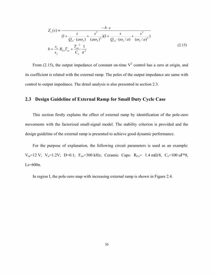
2.3 Design Guideline of External Ramp for Small Duty Cycle Case
This section firstly explains the effect of external ramp by identification of the pole-zero
movements with the factorized small-signal model. The stability criterion is provided and the
design guideline of the external ramp is presented to achieve good dynamic performance.
For the purpose of explanation, the following circuit parameters is used as an example:
Vin=12 V; Vo=1.2V; D=0.1; Fsw=300 kHz; Ceramic Caps: RCo= 1.4 mΩ/8, Co=100 uF*8,
Ls=600n.
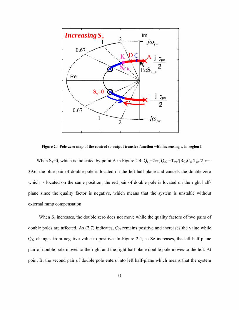
In region I, the pole-zero map with increasing external ramp is shown in Figure 2.4.
2
2
22
2
222
2
2
21
1
))/()/(
1)()()(
1()(
o
swswCo
f
e
ee
o
C
TTR
s
sb
a
s
aQ
s
a
s
aQ
ssb
sZ
(2.15)
31
Figure 2.4 Pole-zero map of the control-to-output transfer function with increasing se in region I
When Se=0, which is indicated by point A in Figure 2.4. Qe1=2/π, Qe2 =Tsw/[RCoCo-Ton/2]π=-
39.6, the blue pair of double pole is located on the left half-plane and cancels the double zero
which is located on the same position; the red pair of double pole is located on the right half-
plane since the quality factor is negative, which means that the system is unstable without
external ramp compensation.
When Se increases, the double zero does not move while the quality factors of two pairs of
double poles are affected. As (2.7) indicates, Qe1 remains positive and increases the value while
Qe2 changes from negative value to positive. In Figure 2.4, as Se increases, the left half-plane
pair of double pole moves to the right and the right-half plane double pole moves to the left. At
point B, the second pair of double pole enters into left half-plane which means that the system
9 . 4 2 e + 0 0 5
9 . 4 2 e + 0 0 5
0 . 7 5
0 . 5 0 . 2 5
0 . 7 5
0 . 5 0 . 2 5
21
0.67
21
0.67
Im
ReB
CD
Increasing Se
:Se_c
K
Se_k
2j ωsw
2j ωsw
swjω
swjω
A
Se=0
32
becomes stable. From (2.7), the stability criterion for external ramp to stabilize the system can be
solved as follows:
)2(4
02
)12( _ DCL
TVssor
D
s
s
os
swocee
f
e
(2.16)
After point B, this pair of double pole moves further into left-half plane, through point C,
and D, until at point K, these two pairs of double poles are located at the same position. The
external ramp needed to reach point K is shown in (2.8) and the quality factor at point K is
shown in (2.9).
Figure 2.5 compares Bode plots of control-to-output transfer function with different external
ramps in this Region. It is clearly shown that with larger external ramp, the peaking of the gain
curve at half the switching frequency is smaller since Qe2 is smaller. From design point of view,
key point K is the best point in this region, since Qe2 is smallest and the system has the highest
damping.
From physical point of view, in this region, since external ramp is in phase with the ESR
ripple, by adding external ramp, the capacitor ripple delay effect which causes the sub-harmonic
problem is reduced. Therefore the instability issue is solved and dynamic performance improves.
33
Figure 2.5. Bode plots comparison of control-to-output transfer function in region I
Further increase the external ramp after the key point K, The two pairs of double poles
separate, as shown in the equations in region II. The pole-zero maps with increasing external
ramp in this Region is shown in Figure 2.6. One pair moves to a higher frequency while the other
pair moves to a lower frequency, and these two pairs of double poles have the same quality
factor which is also a function of external ramp, as shown in (2.11) and (2.13).
1 104 1 10
5170
110
50
101 10
4 1 105
10
0
10
20
30
1 104 1 10
5170
110
50
101 10
4 1 105
10
0
10
20
30
Gai
n/d
B
Fsw/2
Ph
ase/
deg
Frequency/Hz1 10
4 1 105
170
110
50
101 10
4 1 105
10
0
10
20
30
se =0.3sf
Qe2=18
se =1sf,
Qe2=3.4se =1.5sf,
Qe2=1.3
34
Figure 2.6. Pole-zero map of the control-to-output transfer function with increasing se in region II.
Figure 2.7 is comparison of bode plots of control-to-output transfer function with different
external ramps, including both region I and region II. On one hand, separating the two pairs of
poles is beneficial for the stability margin since it pushes one pair of double pole to a frequency
higher than half the switching frequency and therefore reduces the peaking of the gain curve.
This point is verified in Figure 2.7, which shows that the peaking of gain curve with Se=3Sf and
Se=6Sf is less than the peaking of gain curve at key point with Se=1.5Sf. On the other hand,
separating the two pairs of double poles too far apart is not preferred due to the following two
reasons: firstly, the lower frequency double pole will cause phase drop in lower frequency range
9 . 4 2 e + 0 0 5
9 . 4 2 e + 0 0 5
0 . 7 5
0 . 5 0 . 2 5
0 . 7 5
0 . 5 0 . 2 5
21
0.67
21
0.67
Im
Re
2j ωsw
2j ωsw
swjω
swjω
CDK
Increasing Se
F
F

35
and this low frequency double pole slows the transient performance. Secondly, the peaking of the
double poles will be larger which can be seen in (2.13): as variable a increases, Qe1 and Qe2 both
increase. This point is also verified in Figure 2.7, which shows that the peaking of gain curve
with Se=12Sf and Se=20Sf is larger than the peaking of the gain curve with Se=3Sf and Se=6Sf.
Figure 2.7 Bode plots comparison of control-to-output transfer function in region I and II.
The output impedance with small duty cycle case is shown in (2.16). And the comparisons
of output impedance with different external ramp compensations are shown in Figure 2.8.
1 104 1 10
5180
90
0
9020
10
0
10
20
30
Ph
ase/
deg
rees
Se=1.5Sf
Gai
n/d
B
Frequency/Hz
Fsw/2 Se=0.3SfSe=1Sf
Se=3Sf
Se=6Sf
Se=12Sf
Se=20Sf
36
Figure 2.8 Bode plots comparison of output impedance in region I and II.
As can be seen, the output impedance of constant on-time V2 control is very small, however,
the stability margin can also been reflected in the output impedance. When external ramp is too
small, the large peaking occurs in the gain plot which is caused by the capacitor delay. When
external ramp is too large, large peaking also occurs since the quality factor of the low frequency
double pole is increasing. Besides, the output impedance in the low frequency increases since the
coefficient b in (2.16) is proportional to the external ramp. Therefore, either too small or too
large external ramp is detrimental to the load transient performance, which is shown in section
2.5.
From the above analysis, it is clear that neither too small nor too large external ramp is good
for the dynamic performance. To achieve enough stability margin for good dynamic performance,
1 103 1 10
4 1 105 1 10
6100
80
60
40
20Fsw/2
Gai
n/dB
Frequency (Hz)
Se=1.5Sf
Se=0.3Sf
Se=1Sf
Se=3Sf
Se=6Sf
Se=20Sf
Se=12Sf
37
on one hand, the external ramp should be designed larger than Se_k which is the key point K. On
the other hand, the external ramp should not be too large to avoid the lower dominant double
pole. The recommended external ramp slope is within the region of Se_k to 4Se_k. For example,
Se=2Se_k can be chosen. Based on the factorized small-signal model shown in previous section,
the proposed external ramp can be calculated as follows:
22
_ )21(88
)21(2:Preferred D
CL
TVs
Dsss
os
swofkeee
(2.17)
In this example, Se=3Sf is preferred, which is black curve as shown in Figure 2.7 and Figure
2.8. Design example and Simplis simulation verification are provided in Section 2.5.
2.4 The Effect of Duty Cycle and Switching Frequency
This section discusses the effect of the circuit parameters.
In previous section, the design consideration is under the assumption of small duty cycle.
When duty cycle is becoming larger, then the effect of the double pole locate at ω1 is becoming
more and more obvious. For example, when D=0.1, ω1=5ωsw, that is why the effect of the double
pole can be neglected. However, with increasing duty cycle, this pair of double pole is becoming
closer and closer to switching frequency. When D=0.5, ω1=ωsw, which just locates at switching
frequency. When D=0.75, ω1=2/3ωsw, which is very close to half of the switching frequency.
Therefore, additional delay exists for large duty cycle case and it needs to be considered when
designing the outer loop compensation.
38
Besides of the additional delay for large duty cycle case, it is found that the peaking of the
control-to-output transfer function is also related with duty cycle. Referring to (2.9), the quality
factor Qe2 at key point is related with duty cycle, which is rewritten in the following:
21
14:pointKey _21
D
QQQ Keee
(2.18)
From (2.18), Qe_k is related with duty cycle and α. For ceramic caps, if the switching
frequency is not very high, α is very small: for example, for 1.4 mΩ/100uF, with 300kHz
switching frequency, α is only 0.04. α increases as switching frequency increases, which will be
discussed later in this section. The relation between Qe_k and D is plotted as Figure 2.9 with
given switching frequency Fsw=300kHz. It is obvious that with increasing duty cycle, the
minimum quality factor Qe_k is increasing. Qe_k is nearly 7 when D equals to 0.9 which indicates
that the dynamic performance with large duty cycle is very bad.
39
Figure 2.9. The relations between Qe_k and D with Fsw=300kHz.
0 0.1 0.2 0.3 0.4 0.5 0.6 0.7 0.8 0.9 10
2
4
6
8
D
Fsw= 300kkeQ _
1.3
2.2
7.0
1 104 1 10
5180
135
90
45
0
45
90 4 510
0
10
20
30
Frequency
Fsw/2D=0.5 se =0.87se_k
se=0.93se_k
se=se_k
se=2se_k
se=4se_k
se=8se_k
se=12se_k
1 104 1 10
5180
135
90
45
0
45
9010
0
10
20
30
Gai
n/d
BP
has
e/d
egre
es
Frequency
Fsw/2D=0.1se =0.2se_k
se=2/3 se_k
se=se_k
se=2se_k
se=4se_k
se=8se_k
se=13se_k
1 104 1 10
5180
135
90
45
0
45
9010
0
10
20
30
Fsw/2D=0.9 se=se_k
se=2se_k
se=4se_k
se=8se_k
se=12se_k
Frequency
40
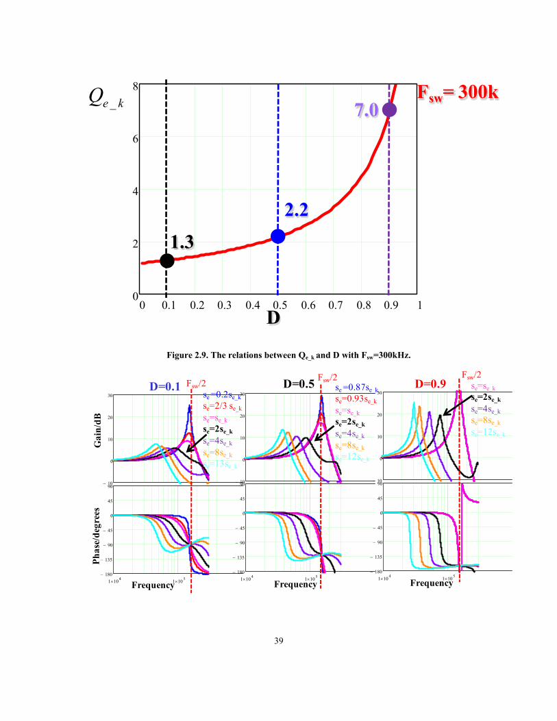
Figure 2.10 Bode plots comparisons of control-to-output transfer function with different Se for D=0.1,
0.5 and 0.9
Figure 2.11 Bode plots comparisons of output impedance with different Se between D=0.1, 0.5 and 0.9
The Bode plots of control-to-output transfer function and output impedance when duty cycle
is 0.1 0.5 and 0.9 are shown in Figure 2.10 and Figure 2.11, respectively. Compare these three
graphs of control to output transfer function, several points can be seen: first, for D=0.1 the
phase at half of switching frequency is around -90 deg, for D=0.5, the phase is around -135 deg
and for D=0.9, the phase is around -165 deg. These different phase delay reveals the effect of the
additional double pole. The large duty cycle, the more phase delay effect caused by this double
pole. Second, for D=0.5 and D=0.9 cases, the effect of different external ramp is very similar
with D=0.1 case: in region I, increasing external ramp reduces the peaking at half the switching
frequency; in region II, increasing external ramp separate the two double poles and also increases
the quality factor of the double poles. From the bode plots, it is also obvious that preferred
external ramp in these cases is also around 2Se_k, which is the same as D=0.1 case. Third,
compare the gain plots of D=0.1, D=0.5 and D=0.9 cases, it is clearly that the peaking increases
with increasing duty cycle. At D=0.5, the peaking is around 10dB and at D=0.9 the peaking is
1 103 1 10
4 1 105
100
80
60
40
20
1 103 1 10
4 1 105
100
80
60
40
20
1 103 1 10
4 1 105
100
80
60
40
20Fsw/2
Gai
n/d
B
Frequency (Hz)
Fsw/2 Fsw/2
Frequency (Hz) Frequency (Hz)
Se=2Se_kSe=2Se_k
Se=2Se_k
D=0.5D=0.1 D=0.9
41
around 20dB. In these two cases, only using external ramp is not enough for good dynamic
performance. From the output impedance in Figure 2.11, it is also shown that preferred external
ramp in these cases is also around 2Se_k, which is shown as black curve in each case. Compare
the magnitude with different duty cycle cases, it can be seen that when duty cycle is larger, not
only the damping is worse; the low frequency magnitude of the output impedance also increases.
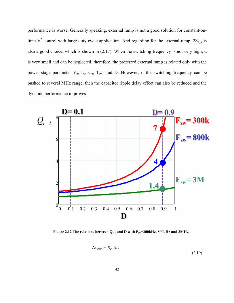
However, the situation changes if the switching frequency is becoming higher and higher,
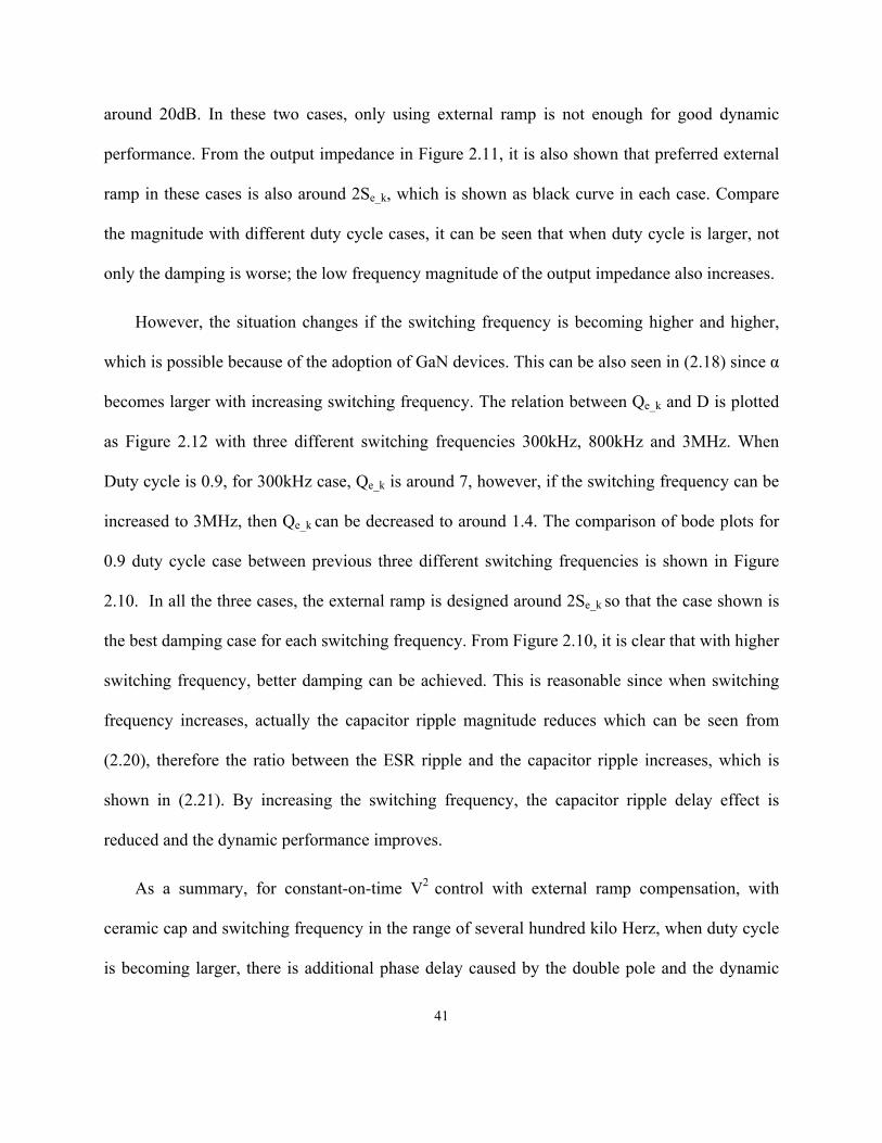
which is possible because of the adoption of GaN devices. This can be also seen in (2.18) since α
becomes larger with increasing switching frequency. The relation between Qe_k and D is plotted
as Figure 2.12 with three different switching frequencies 300kHz, 800kHz and 3MHz. When
Duty cycle is 0.9, for 300kHz case, Qe_k is around 7, however, if the switching frequency can be
increased to 3MHz, then Qe_k can be decreased to around 1.4. The comparison of bode plots for
0.9 duty cycle case between previous three different switching frequencies is shown in Figure
2.10. In all the three cases, the external ramp is designed around 2Se_k so that the case shown is
the best damping case for each switching frequency. From Figure 2.10, it is clear that with higher
switching frequency, better damping can be achieved. This is reasonable since when switching
frequency increases, actually the capacitor ripple magnitude reduces which can be seen from
(2.20), therefore the ratio between the ESR ripple and the capacitor ripple increases, which is
shown in (2.21). By increasing the switching frequency, the capacitor ripple delay effect is
reduced and the dynamic performance improves.
As a summary, for constant-on-time V2 control with external ramp compensation, with
ceramic cap and switching frequency in the range of several hundred kilo Herz, when duty cycle
is becoming larger, there is additional phase delay caused by the double pole and the dynamic
42
performance is worse. Generally speaking, external ramp is not a good solution for constant-on-
time V2 control with large duty cycle application. And regarding for the external ramp, 2Se_k is
also a good choice, which is shown in (2.17). When the switching frequency is not very high, α
is very small and can be neglected, therefore, the preferred external ramp is related only with the
power stage parameter Vo, Ls, Co, Tsw, and D. However, if the switching frequency can be
pushed to several MHz range, then the capacitor ripple delay effect can also be reduced and the
dynamic performance improves.
Figure 2.12 The relations between Qe_k and D with Fsw=300kHz, 800kHz and 3MHz.
LCoESR iRv
(2.19)
0 0.1 0.2 0.3 0.4 0.5 0.6 0.7 0.8 0.9 10
2
4
6
8
Fsw= 800k
D
Fsw= 300k
Fsw= 3M
D= 0.1 D= 0.9keQ _
7
4
1.4
43
swLo
Co TiC
v 8
1 (2.20)
88
sw
oCo
Co
ESR
T
CR
v
v (2.21)
Figure 2.13 Bode plots comparison of control-to-output transfer function with different switching frequencies.
2.5 External Ramp Design Example and Simplis Simulation Verification
10
0
10
20
30
1 104 1 10
5 1 106 1 10
7180
135
90
45
0
Fsw=300kHz
Fsw=800kHz
Fsw=3MHz
Frequency
Gai
n/d
BP
has
e/d
egre
es
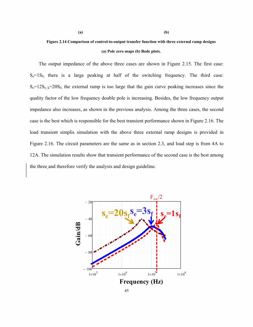
44
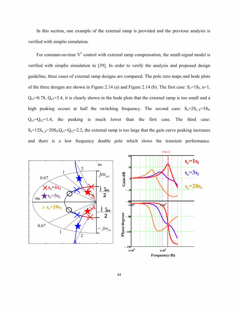
In this section, one example of the external ramp is provided and the previous analysis is
verified with simplis simulation.
For constant-on-time V2 control with external ramp compensation, the small-signal model is
verified with simplis simulation in [39]. In order to verify the analysis and proposed design
guideline, three cases of external ramp designs are compared. The pole zero maps and bode plots
of the three designs are shown in Figure 2.14 (a) and Figure 2.14 (b). The first case: Se=1Sf, a=1,
Qe1=0.78, Qe2=3.4, it is clearly shown in the bode plots that the external ramp is too small and a
high peaking occurs at half the switching frequency. The second case: Se=2Se_k=3Sf,
Qe1=Qe2=1.4, the peaking is much lower than the first case. The third case:
Se=12Se_k=20Sf,Qe1=Qe2=2.2, the external ramp is too large that the gain curve peaking increases
and there is a low frequency double pole which slows the transient performance.
9 . 4 2 e + 0 0 5
9 . 4 2 e + 0 0 5
0 . 7 5
0 . 5 0 . 2 5
0 . 7 5
0 . 5 0 . 2 5
21
0.67
21
0.67
Im
Re
2j ωsw
2j ωsw
swjω
swjω
∆
∆
∆
1 104 1 10
520
10
0
10
20
1 104 1 10
5170
110
50
10
1 104 1 10
520
10
0
10
20
Gai
n/d
B
1 104 1 10
5170
110
50
10
Ph
ase/
deg
rees
Frequency\Hz
Fsw/2
1 104 1 10
520
10
0
10
20
1 104 1 10
5170
110
50
10
se=1sf
se=3sf
se=20sf
∆
se=1sf
se=20sf
se=3sf
45
(a) (b)
Figure 2.14 Comparison of control-to-output transfer function with three external ramp designs
(a) Pole zero maps (b) Bode plots.
The output impedance of the above three cases are shown in Figure 2.15. The first case:
Se=1Sf, there is a large peaking at half of the switching frequency. The third case:
Se=12Se_k=20Sf, the external ramp is too large that the gain curve peaking increases since the
quality factor of the low frequency double pole is increasing. Besides, the low frequency output
impedance also increases, as shown in the previous analysis. Among the three cases, the second
case is the best which is responsible for the best transient performance shown in Figure 2.16. The
load transient simplis simulation with the above three external ramp designs is provided in
Figure 2.16. The circuit parameters are the same as in section 2.3, and load step is from 4A to
12A. The simulation results show that transient performance of the second case is the best among
the three and therefore verify the analysis and design guideline.
1 103 1 10
4 1 105 1 10
6100
80
60
40
20Fsw/2
Gai
n/d
B
Frequency (Hz)
se=3sfse=20sf se=1sf
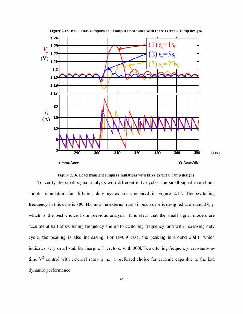
46
Figure 2.15. Bode Plots comparison of output impedance with three external ramp designs
Figure 2.16. Load transient simplis simulations with three external ramp designs
To verify the small-signal analysis with different duty cycles, the small-signal model and
simplis simulation for different duty cycles are compared in Figure 2.17. The switching
frequency in this case is 300kHz, and the external ramp in each case is designed at around 2Se_k,
which is the best choice from previous analysis. It is clear that the small-signal models are
accurate at half of switching frequency and up to switching frequency, and with increasing duty
cycle, the peaking is also increasing. For D=0.9 case, the peaking is around 20dB, which
indicates very small stability margin. Therefore, with 300kHz switching frequency, constant-on-
time V2 control with external ramp is not a preferred choice for ceramic caps due to the bad
dynamic performance.
1.17
1.18
1.19
1.2
1.21
1.22
1.23
1.24
time/uSecs 10uSecs/div
290 300 310 320 330 340 3500
5
10
15
20
1.17
1.18
1.19
1.2
1.21
1.22
1.23
1.24
290 300 310 320 330 340 3500
5
10
15
20
1.17
1.18
1.19
1.2
1.21
1.22
1.23
1.24
time/uSecs 10uSecs/div
290 300 310 320 330 340 3500
5
10
15
20
1.17
1.18
1.19
1.2
1.21
1.22
1.23
1.24
time/uSecs 10uSecs/div
290 300 310 320 330 340 3500
5
10
15
20
Vo
iL
(V)
(A)
(us)
(1) se=1sf
(2) se=3sf
(3) se=20sf
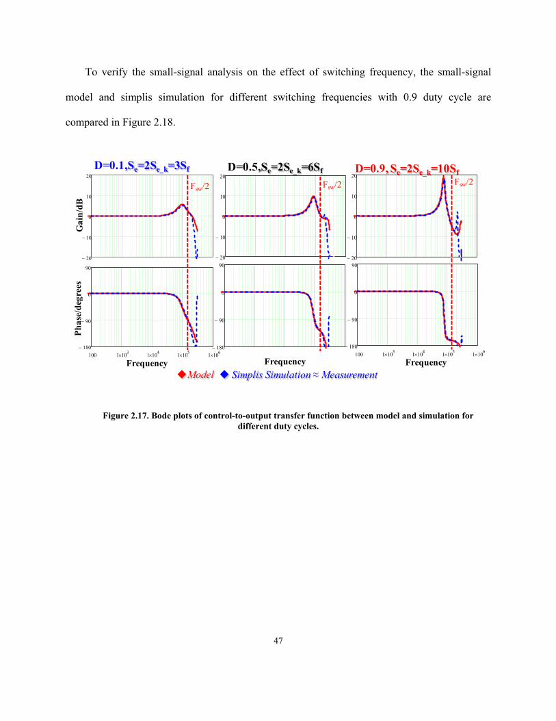
47
To verify the small-signal analysis on the effect of switching frequency, the small-signal
model and simplis simulation for different switching frequencies with 0.9 duty cycle are
compared in Figure 2.18.
Figure 2.17. Bode plots of control-to-output transfer function between model and simulation for different duty cycles.
D=0.5,Se=2Se_k=6Sf
20
10
0
10
20
Frequency
180
90
0
90
Fsw/2
D=0.9, Se=2Se_k=10Sf
3 4 5 620
10
0
10
20
Frequency100 1 10
3 1 104 1 10
5 1 106
180
90
0
90
Fsw/2
20
10
0
10
20
100 1 103 1 10
4 1 105 1 10
6180
90
0
90
Frequency
Fsw/2
Gai
n/d
BP
has
e/d
egre
es
D=0.1,Se=2Se_k=3Sf
Model Simplis Simulation ≈ Measurement
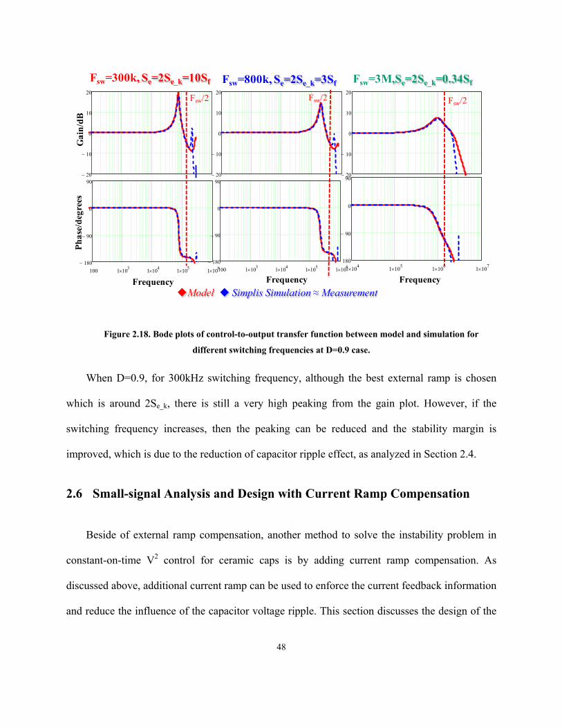
48
Figure 2.18. Bode plots of control-to-output transfer function between model and simulation for
different switching frequencies at D=0.9 case.
When D=0.9, for 300kHz switching frequency, although the best external ramp is chosen
which is around 2Se_k, there is still a very high peaking from the gain plot. However, if the
switching frequency increases, then the peaking can be reduced and the stability margin is
improved, which is due to the reduction of capacitor ripple effect, as analyzed in Section 2.4.
2.6 Small-signal Analysis and Design with Current Ramp Compensation
Beside of external ramp compensation, another method to solve the instability problem in
constant-on-time V2 control for ceramic caps is by adding current ramp compensation. As
discussed above, additional current ramp can be used to enforce the current feedback information
and reduce the influence of the capacitor voltage ripple. This section discusses the design of the
20
10
0
10
20
Model Simplis Simulation ≈ Measurement
20
10
0
10
20
Fsw=800k, Se=2Se_k=3Sf
Frequency
Fsw/2
100 1 103 1 10
4 1 105 1 10
6180
90
0
90
Fsw=3M,Se=2Se_k=0.34Sf
Frequency
Fsw/2
Fsw=300k, Se=2Se_k=10Sf
3 4 5 620
10
0
10
20
Frequency100 1 10
3 1 104 1 10
5 1 106
180
90
0
90
Fsw/2
Gai
n/d
BP
has
e/d
egre
es
1 104 1 10
5 1 106 1 10
7180
90
0
90
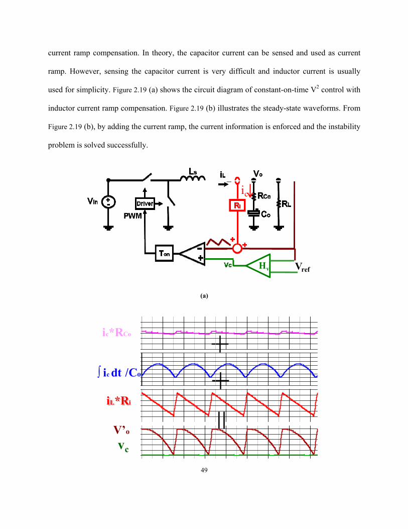
49
current ramp compensation. In theory, the capacitor current can be sensed and used as current
ramp. However, sensing the capacitor current is very difficult and inductor current is usually
used for simplicity. Figure 2.19 (a) shows the circuit diagram of constant-on-time V2 control with
inductor current ramp compensation. Figure 2.19 (b) illustrates the steady-state waveforms. From
Figure 2.19 (b), by adding the current ramp, the current information is enforced and the instability
problem is solved successfully.
(a)
Hv Vref
ic
∫ ic dt /Co
V’o
ic*RCo
iL*Ri
+
=
+
vc
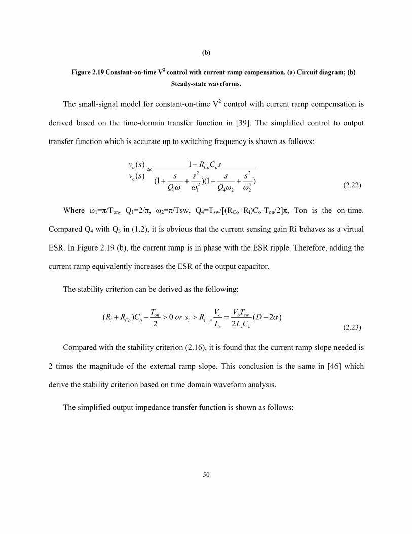
50
(b)
Figure 2.19 Constant-on-time V2 control with current ramp compensation. (a) Circuit diagram; (b)
Steady-state waveforms.
The small-signal model for constant-on-time V2 control with current ramp compensation is
derived based on the time-domain transfer function in [39]. The simplified control to output
transfer function which is accurate up to switching frequency is shown as follows:
)1)(1(
1
)(
)(
22
2
2421
2
11 s
Q
ss
Q
s
sCR
sv
sv oCo
c
o
(2.22)
Where ω1=π/Ton, Q1=2/π, ω2=π/Tsw, Q4=Tsw/[(RCo+Ri)Co-Ton/2]π, Ton is the on-time.
Compared Q4 with Q3 in (1.2), it is obvious that the current sensing gain Ri behaves as a virtual
ESR. In Figure 2.19 (b), the current ramp is in phase with the ESR ripple. Therefore, adding the
current ramp equivalently increases the ESR of the output capacitor.
The stability criterion can be derived as the following:
)2(2
02
)( _ DCL
TV
L
VRsor
TCRR
os
swo
s
ocii
onoCoi
(2.23)
Compared with the stability criterion (2.16), it is found that the current ramp slope needed is
2 times the magnitude of the external ramp slope. This conclusion is the same in [46] which
derive the stability criterion based on time domain waveform analysis.
The simplified output impedance transfer function is shown as follows:
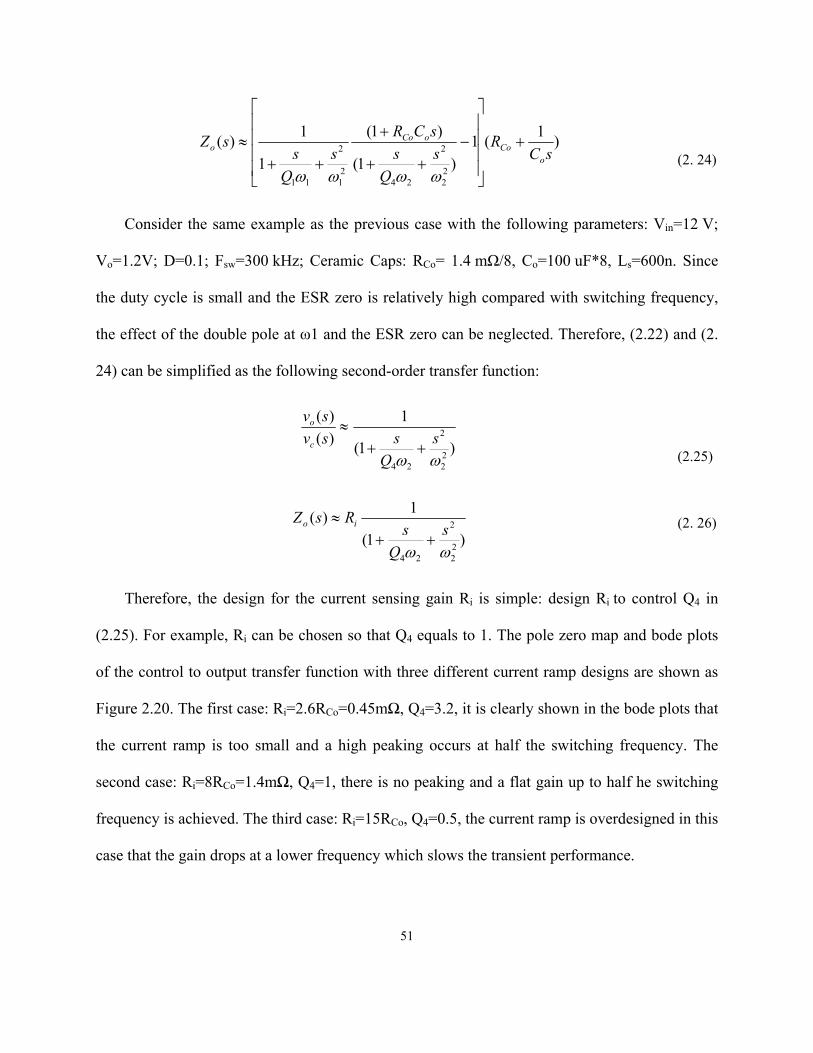
51
)1
(1
)1(
)1(
1
1)(
22
2
2421
2
11
sCR
s
Q
s
sCR
s
Q
ssZ
oCo
oCoo
(2. 24)
Consider the same example as the previous case with the following parameters: Vin=12 V;
Vo=1.2V; D=0.1; Fsw=300 kHz; Ceramic Caps: RCo= 1.4 mΩ/8, Co=100 uF*8, Ls=600n. Since
the duty cycle is small and the ESR zero is relatively high compared with switching frequency,
the effect of the double pole at ω1 and the ESR zero can be neglected. Therefore, (2.22) and (2.
24) can be simplified as the following second-order transfer function:
)1(
1
)(
)(
22
2
24 s
Q
ssv
sv
c
o
(2.25)
)1(
1)(
22
2
24 s
Q
sRsZ io
(2. 26)
Therefore, the design for the current sensing gain Ri is simple: design Ri to control Q4 in
(2.25). For example, Ri can be chosen so that Q4 equals to 1. The pole zero map and bode plots
of the control to output transfer function with three different current ramp designs are shown as
Figure 2.20. The first case: Ri=2.6RCo=0.45mΩ, Q4=3.2, it is clearly shown in the bode plots that
the current ramp is too small and a high peaking occurs at half the switching frequency. The
second case: Ri=8RCo=1.4mΩ, Q4=1, there is no peaking and a flat gain up to half he switching
frequency is achieved. The third case: Ri=15RCo, Q4=0.5, the current ramp is overdesigned in this
case that the gain drops at a lower frequency which slows the transient performance.
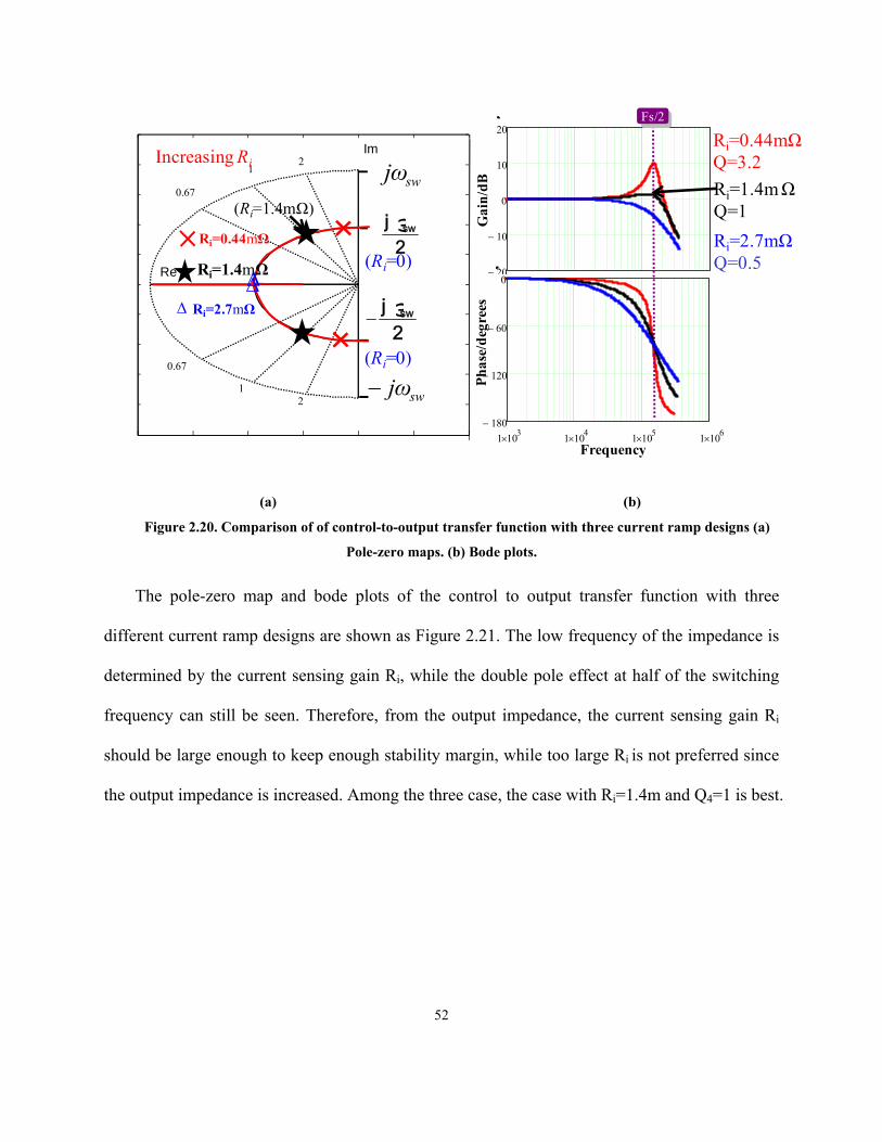
52
(a) (b)
Figure 2.20. Comparison of of control-to-output transfer function with three current ramp designs (a)
Pole-zero maps. (b) Bode plots.
The pole-zero map and bode plots of the control to output transfer function with three
different current ramp designs are shown as Figure 2.21. The low frequency of the impedance is
determined by the current sensing gain Ri, while the double pole effect at half of the switching
frequency can still be seen. Therefore, from the output impedance, the current sensing gain Ri
should be large enough to keep enough stability margin, while too large Ri is not preferred since
the output impedance is increased. Among the three case, the case with Ri=1.4m and Q4=1 is best.
1 103 1 10
4 1 105 1 10
6180
120
60
020
10
0
10
20Fs/2
Ri=0.44mΩQ=3.2
Gai
n/d
BP
has
e/d
egre
es
Frequency
Ri=1.4mΩQ=1
Ri=2.7mΩQ=0.5
9 . 4 2 e + 0 0 5
9 . 4 2 e + 0 0 5
0 . 7 5
0 . 5 0 . 2 5
0 . 7 5
0 . 5 0 . 2 5
21
0.67
21
0.67
Im
Re
2j ωsw
2j ωsw
swjω
swjω
Increasing Ri
(Ri=1.4mΩ)
(Ri=0)
(Ri=0)
∆∆∆
Ri=0.44mΩ
Ri=2.7mΩ
Ri=1.4mΩ
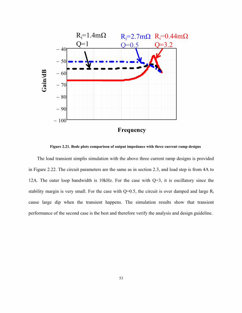
53
Figure 2.21. Bode plots comparison of output impedance with three current ramp designs
The load transient simplis simulation with the above three current ramp designs is provided
in Figure 2.22. The circuit parameters are the same as in section 2.3, and load step is from 4A to
12A. The outer loop bandwidth is 10kHz. For the case with Q=3, it is oscillatory since the
stability margin is very small. For the case with Q=0.5, the circuit is over damped and large Ri
cause large dip when the transient happens. The simulation results show that transient
performance of the second case is the best and therefore verify the analysis and design guideline.
100
90
80
70
60
50
40
Ri=0.44mΩQ=3.2
Ri=1.4mΩQ=1
Ri=2.7mΩQ=0.5
Gai
n/d
B
Frequency

54
Figure 2.22. Load transient simulations with three different current ramp designs
For the application of different duty cycles, from (2.22), when duty cycle is becoming larger,
the effect of the double pole located at ω1 is becoming more obvious and the additional delay
caused by this double pole should be considered when designing the outer loop. However, with
current ramp compensation, the peaking at half of the switching frequency can be well controlled
by designing the current ramp appropriately. For example, from (2.22), the current ramp can be
designed so that the quality factor is around 1. This is quite different compared with external
ramp compensation method where the best dynamic performance can be achieved is related with
duty cycle and the current feedback strength α, as shown in (2.18). It is already shown in Section
2.4 that when duty cycle is larger, the damping performance with external ramp compensation is
very bad, unless very high switching frequency is used. The current ramp needed is shown in
equation (2.27).
1.17
1.18
1.19
1.2
1.21
1.22
480 490 500 510 520 530 5400
5
10
15
20
25
1.17
1.18
1.19
1.2
1.21
1.22
480 490 500 510 520 530 5400
5
10
15
20
25
Vo
iL
(us)
1.17
1.18
1.19
1.2
1.21
1.22
480 490 500 510 520 530 5400
5
10
15
20
25
1.17
1.18
1.19
1.2
1.21
1.22
480 490 500 510 520 530 5400
5
10
15
20
25
(1)Current ramp (Ri=0.44mΩ,Q=3.2)(2)Current ramp (Ri=1.4mΩ ,Q=1)(3)Current ramp (Ri=2.7mΩ ,Q=0.5)
55
CooCo
swi R
CR
TDR
1
2
1
(2.27)
2.7 Summary
This chapter investigates the characteristic for constant-on-time V2 control with external
ramp compensation by factorizing the small-signal control-to-output transfer function. It is found
that with increasing the external ramp, two pairs of double poles first move toward each other at
half of switching frequency, after meeting at the key point, the two double poles separate, one
moves to a lower frequency and the other moves to a higher frequency while keeping the quality
factor equal to each other. For the output impedance, with increasing external ramp, the
magnitude in the low frequency also increases. Based on that, design guideline is provided to
achieve good dynamic performance. The recommended external ramp is around two times the
magnitude at the key point K. When duty cycle is larger, the damping performance is not good
with only external ramp compensation, unless very high switching frequency is used. With
current ramp compensation, it is recommended to design the current ramp so that the quality
factor of the double pole is around 1. With current ramp compensation, the damping can be well
controlled regardless of the circuit parameters.
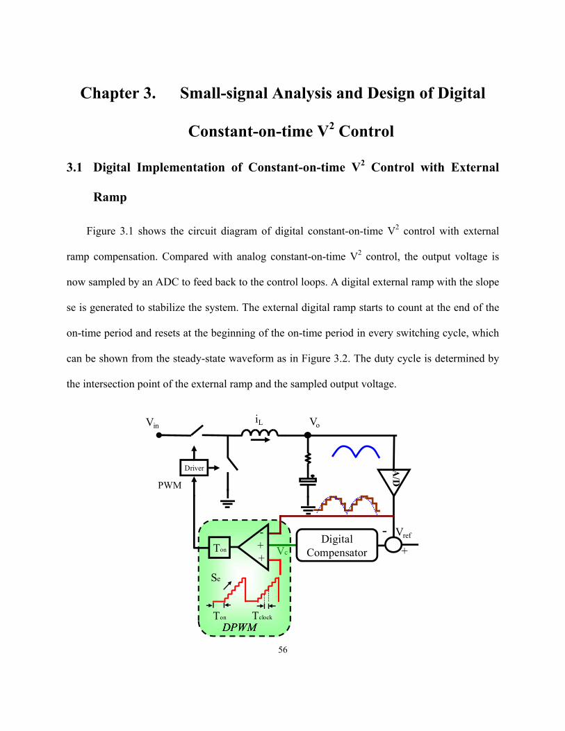
56
Chapter 3. Small-signal Analysis and Design of Digital
Constant-on-time V2 Control
3.1 Digital Implementation of Constant-on-time V2 Control with External
Ramp
Figure 3.1 shows the circuit diagram of digital constant-on-time V2 control with external
ramp compensation. Compared with analog constant-on-time V2 control, the output voltage is
now sampled by an ADC to feed back to the control loops. A digital external ramp with the slope
se is generated to stabilize the system. The external digital ramp starts to count at the end of the
on-time period and resets at the beginning of the on-time period in every switching cycle, which
can be shown from the steady-state waveform as in Figure 3.2. The duty cycle is determined by
the intersection point of the external ramp and the sampled output voltage.
Vc+-
Ton
VrefDigitalCompensator +
-
DPWM
A/D
Vin Vo
Driver
PWM
iL
DPWM
Se
Ton Tclock
+
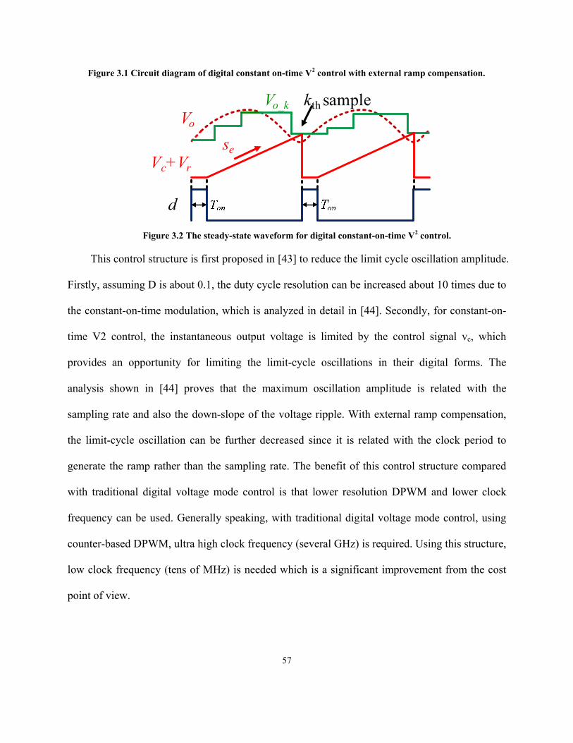
57
Figure 3.1 Circuit diagram of digital constant on-time V2 control with external ramp compensation.
Figure 3.2 The steady-state waveform for digital constant-on-time V2 control.
This control structure is first proposed in [43] to reduce the limit cycle oscillation amplitude.
Firstly, assuming D is about 0.1, the duty cycle resolution can be increased about 10 times due to
the constant-on-time modulation, which is analyzed in detail in [44]. Secondly, for constant-on-
time V2 control, the instantaneous output voltage is limited by the control signal vc, which
provides an opportunity for limiting the limit-cycle oscillations in their digital forms. The
analysis shown in [44] proves that the maximum oscillation amplitude is related with the
sampling rate and also the down-slope of the voltage ripple. With external ramp compensation,
the limit-cycle oscillation can be further decreased since it is related with the clock period to
generate the ramp rather than the sampling rate. The benefit of this control structure compared
with traditional digital voltage mode control is that lower resolution DPWM and lower clock
frequency can be used. Generally speaking, with traditional digital voltage mode control, using
counter-based DPWM, ultra high clock frequency (several GHz) is required. Using this structure,
low clock frequency (tens of MHz) is needed which is a significant improvement from the cost
point of view.
Vo
Vc+Vr
d
Vo_k
se
kth sample
58
However, the concern about this structure is the external ramp design. From the limit cycle
oscillation point of view, the larger the external ramp, the smaller the magnitude of oscillation.
However, as shown in [44], the selection of the external ramp is not only related to the amplitude
of the limit-cycle oscillation, but also very important to the stability of the system. Therefore, the
external ramp needs to be designed properly to solve the instability issue and improve the
dynamic performance.
In this chapter, the characteristic for digital constant-on-time V2 with external ramp is
investigated in detail by factorizing the small-signal model derived in [44]. The stability criterion
and the external ramp design guideline are provided and the influence of sampling effect is
investigated and revealed. The small-signal experimental results and load transient result for
digital constant-on-time V2 control are presented to verify the analysis and proposed design
guideline.
3.2 Small-signal Model of Digital Constant-on-time V2 Control with External
Ramp
The small-signal control-to-output transfer function is derived in [44] as follows:
222
2
2222
2
2
22
2
22
21
2
11
)1)(1(
)1)(1(
)1(
1
)(
)(
sTCRs
ss
Q
ss
Q
s
sCRs
Q
s
s
Q
ssv
sv
swoCof
e
d
oCo
c
o
(3.1)
where Tsw is the switching period, RCo is the ESR of the output capacitors, Co is the
capacitance of the output capacitors, ω1=π/Ton, Q1=2/π, ω2=π/Tsw, Q2=2/π, sf=RCoVo/L, L is the
inductance, Qd=Tsw/[RCoCo+Ton/2+int(Toff/Ts)Ts)]π, Ton is the on-time, int(x) is the integer part
59
of x, Toff is the off-time, and Ts is the sampling time of the ADC. Note that the quantization
effects of the ADC and the digital external ramp are ignored during the derivation.
Since ESR zero of the output ceramic capacitor is very high relative to the switching
frequency, for small duty ratio application, the transfer function can be further simplified as
follows:
222
2
2222
2
2
22
2
22
)1)(1(
)1(
)(
)(
sTCRs
ss
Q
ss
Q
s
s
Q
s
sv
sv
swoCof
e
d
c
o
(3.2)
Compare (3.2) with (2.2), it is interesting that these two forms are very similar. Therefore,
the factorization strategy and design strategy of analog constant-on-time V2 can be extended
directly to digital constant-on-time V2 control.
The transfer function (3.2) can be factorized in the following form:
))/()/(
1)()()(
1(
)1(
)(
)(
22
2
222
2
2
21
22
2
22
a
s
aQ
s
a
s
aQ
s
s
Q
s
sv
sv
dede
c
o
(3.3)
where a, Qde1, Qde2 are all real numbers. The factorized results are dividing into two
Regions based on the different amplitudes of the external ramp, which is very similar as analog
case, the factorization details are shown in appendix A.
Region I: for relatively small external ramp.
60
fsw
s
s
sw
sw
s
s
sw
e sT
T
T
DTD
T
T
T
DTD
s
2
1
4
))1(
int(2
1)1(int2
2
(3.4)
Where α is defined the same as in analog case α= RCoCo/Tsw in (2.6).
The expressions of a, Qde1 and Qde2 in (2.4) are shown as follows:
21
112
21
111
)(811
114
)(811
114
1
B
sABQ
B
sABQ
a
e
de
e
de
(3.5)
Where the expression of A1(se) and B1 is shown as follows:
sw
s
s
sw
sw
s
s
sw
f
ee
T
T
T
DTDB
T
T
T
DTD
s
ssA
))1(
int(212
))1(
int(2
)12
()(
1
1
(3.6)
In this region, a=1 means that both pairs of double poles are located at half the switching
frequency. The external ramp changes Qde1 and Qde2, as shown in (2.7). At the key point se=sde_k ,
Qde1 =Qde2=Qde_k, as shown in the following:
fsw
s
s
sw
sw
s
s
sw
Kde sT
T
T
DTD
T
T
T
DTD
s
2
1
4
))1(
int(2
1)1(int2
:pointKey
2
_
(3.7)
61
1_21
14:pointKey
BQQQ Kdedede
(3.8)
Region II: for relatively large external ramp Se>=Sde_k.
The expression of a in (3.3) in this region is shown as follows:
12
4
YYa
(3.9)
21
2
2
1
2
1
2
4)(2
4)(2
BsAsAY ee
(3.10)
The expressions of Qde1 and Qde2 in (2.4) in this region are shown as follows:
)1
(12
121 a
aB
QQ dede (3.11)
The scenario is very similar as for analog case in this region: As external ramp increases,
a>1 means the two pairs of double poles are separated and are not located at half the switching
frequency any more. One pair of double pole moves to a higher frequency while the other pair of
double pole moves to a lower frequency. These two pairs of double poles have the same quality
factor in this region and at the key point Qde2 reach its minimum value.
For the output impedance, the result is derived in [44] as follows:
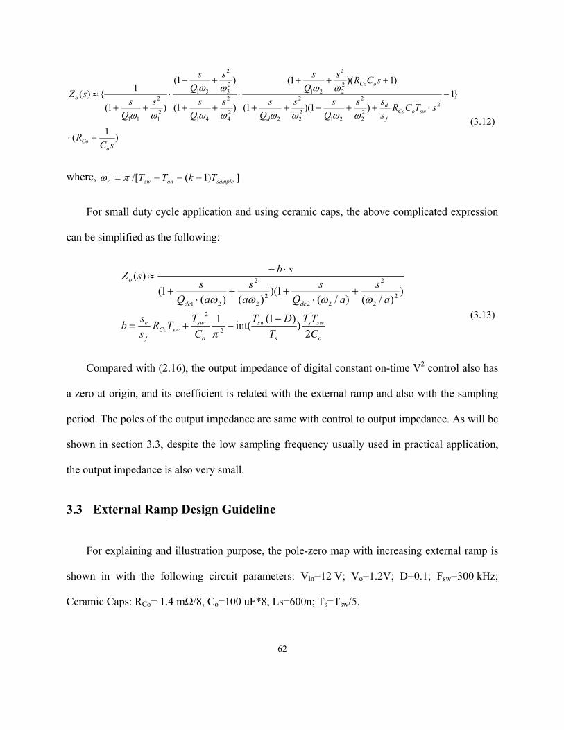
62
where, ])1(/[4 sampleonsw TkTT
For small duty cycle application and using ceramic caps, the above complicated expression
can be simplified as the following:
Compared with (2.16), the output impedance of digital constant on-time V2 control also has
a zero at origin, and its coefficient is related with the external ramp and also with the sampling
period. The poles of the output impedance are same with control to output impedance. As will be
shown in section 3.3, despite the low sampling frequency usually used in practical application,
the output impedance is also very small.
3.3 External Ramp Design Guideline
For explaining and illustration purpose, the pole-zero map with increasing external ramp is
shown in with the following circuit parameters: Vin=12 V; Vo=1.2V; D=0.1; Fsw=300 kHz;
Ceramic Caps: RCo= 1.4 mΩ/8, Co=100 uF*8, Ls=600n; Ts=Tsw/5.
)1
(
1
)1)(1(
)1)(1(
)1(
)1(
)1(
1)(
222
2
2122
2
2
22
2
21
24
2
41
23
2
31
21
2
11
sCR
sTCRs
ss
Q
ss
Q
s
sCRs
Q
s
s
Q
s
s
Q
s
s
Q
ssZ
oCo
swoCof
d
d
oCo
o
(3.12)
o
sws
s
sw
o
swswCo
f
e
dede
o
C
TT
T
DT
C
TTR
s
sb
a
s
aQ
s
a
s
aQ
s
sbsZ
2)
)1(int(
1
))/()/(
1)()()(
1(
)(
2
2
22
2
222
2
2
21
(3.13)
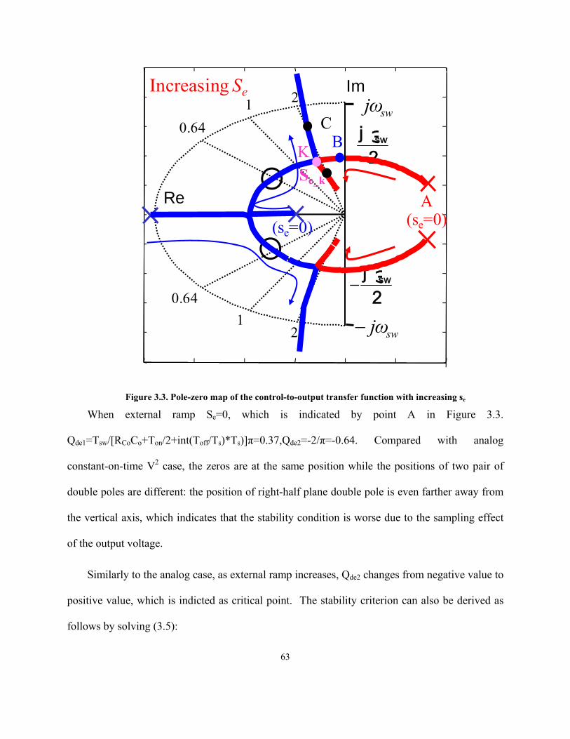
63
Figure 3.3. Pole-zero map of the control-to-output transfer function with increasing se
When external ramp Se=0, which is indicated by point A in Figure 3.3.
Qde1=Tsw/[RCoCo+Ton/2+int(Toff/Ts)*Ts)]π=0.37,Qde2=-2/π=-0.64. Compared with analog
constant-on-time V2 case, the zeros are at the same position while the positions of two pair of
double poles are different: the position of right-half plane double pole is even farther away from
the vertical axis, which indicates that the stability condition is worse due to the sampling effect
of the output voltage.
Similarly to the analog case, as external ramp increases, Qde2 changes from negative value to
positive value, which is indicted as critical point. The stability criterion can also be derived as
follows by solving (3.5):
9 . 4 2 e + 0 0 5
9 . 4 2 e + 0 0 5
0 . 7 5
0 . 5 0 . 2 5
0 . 7 5
0 . 5 0 . 2 5
21
0.64
21
0.64
Im
Re
2j ωsw
2j ωsw
swjω
swjω
Increasing Se
(se=0) (se=0)
KSe_k
A
BC

64
0))1(
int(2
)12(
sw
s
s
sw
f
e
T
T
T
DTD
s
s
(3.14)
Similar as the analog case, at the key point Qde2 has the minimum value, which is shown in
(3.8). The bode plots of control-to-output transfer functions with different external ramps are
shown in Figure 3.4. From the design point of view, for digital constant-on-time V2 control, the
design strategy for external ramp is similar as in analog case. To obtain best dynamic
performance, the external ramp should neither be too small (gain enough damping) or too large
(avoid the low frequency dominant double pole and the phase delay caused by it), it is suggested
that the external ramp designed around the value of key point. In this case Se=15Sf is selected,
which is the black curve with minimum peaking in Figure 3.4 and point C in Figure 3.3.
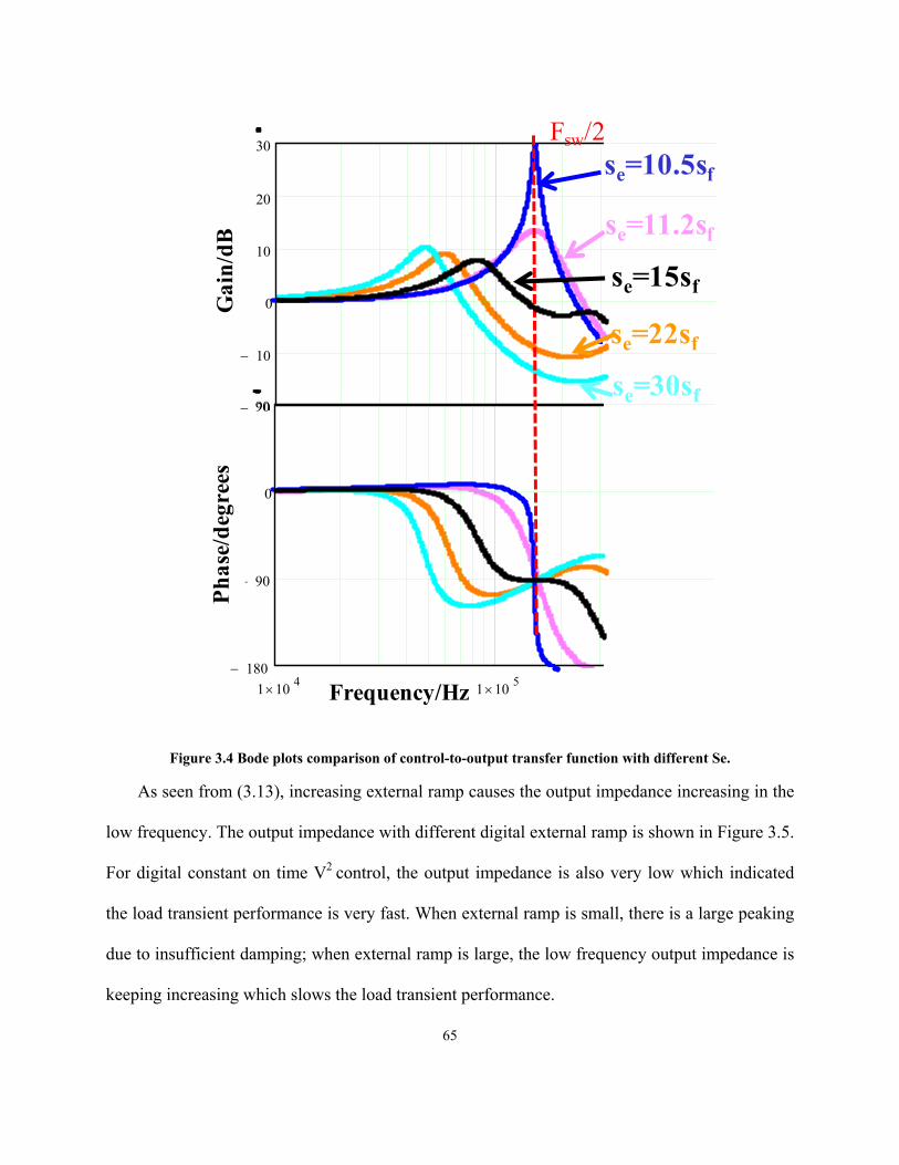
65
Figure 3.4 Bode plots comparison of control-to-output transfer function with different Se.
As seen from (3.13), increasing external ramp causes the output impedance increasing in the
low frequency. The output impedance with different digital external ramp is shown in Figure 3.5.
For digital constant on time V2 control, the output impedance is also very low which indicated
the load transient performance is very fast. When external ramp is small, there is a large peaking
due to insufficient damping; when external ramp is large, the low frequency output impedance is
keeping increasing which slows the load transient performance.
se=22sf
se=11.2sf
se=30sf20
10
0
10
20
30
1 104 1 10
5180
90
0
90
Gai
n/d
BP
has
e/d
egre
es
se=10.5sf
Fsw/2
Frequency/Hz
se=15sf
66
Figure 3.5. Bode plots comparison of output impedance with different digital external ramp.
3.4 Comparison with Analog Constant-on-time V2 Control
To compare the stability criterion of analog and digital case side by side, Equation (2. 14)
and (3.14) are rewritten in the following:
2)12(0
2)12(
D
s
sor
D
s
s
f
e
f
e
(2.16)
sw
s
s
sw
f
e
sw
s
s
sw
f
e
T
T
T
DTD
s
sor
T
T
T
DTD
s
s)
)1(int(2
2)12(0)
)1(int(
2)12(
(3.13)
Compare (2.16) and (3.14), the difference on the right hand side is that for digital case, there
is an additional term which is related with the sampling period. Therefore, larger external ramp is
needed due to the sampling effects. With the given parameters, the stability criterion is Se>0.3Sf
for analog case while the stability criterion is Se>10.3Sf for digital case.
To compare the minimum quality factor of analog and digital case side by side, Equation (2.
14 and (3.8) are rewritten in the following:
Fs/2
Gai
n/d
B
Frequency/Hz1 10
3 1 104 1 10
5 1 106
120
100
80
60
40 se=10.5sfse=11sfse=15sf
se=28sf
se=22sf
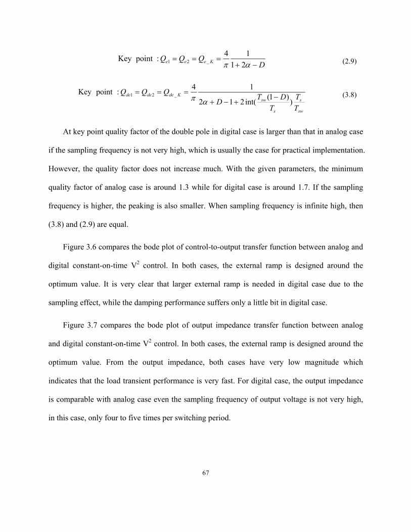
67
DQQQ Keee
21
14:pointKey _21
(2.9)
sw
s
s
swKdedede
T
T
T
DTD
QQQ)
)1(int(212
14:pointKey _21
(3.8)
At key point quality factor of the double pole in digital case is larger than that in analog case
if the sampling frequency is not very high, which is usually the case for practical implementation.
However, the quality factor does not increase much. With the given parameters, the minimum
quality factor of analog case is around 1.3 while for digital case is around 1.7. If the sampling
frequency is higher, the peaking is also smaller. When sampling frequency is infinite high, then
(3.8) and (2.9) are equal.
Figure 3.6 compares the bode plot of control-to-output transfer function between analog and
digital constant-on-time V2 control. In both cases, the external ramp is designed around the
optimum value. It is very clear that larger external ramp is needed in digital case due to the
sampling effect, while the damping performance suffers only a little bit in digital case.
Figure 3.7 compares the bode plot of output impedance transfer function between analog
and digital constant-on-time V2 control. In both cases, the external ramp is designed around the
optimum value. From the output impedance, both cases have very low magnitude which
indicates that the load transient performance is very fast. For digital case, the output impedance
is comparable with analog case even the sampling frequency of output voltage is not very high,
in this case, only four to five times per switching period.
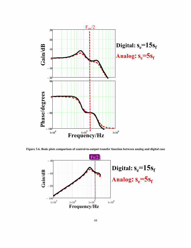
68
Figure 3.6. Bode plots comparison of control-to-output transfer function between analog and digital case
1 104 1 10
5 1 106
180
90
0
9020
10
0
10
20
30
Analog: se=5sf
20
10
0
10
20
30
1 104 1 10
5 1 106
180
90
0
90
Digital: se=15sfG
ain
/dB
Ph
ase/
deg
rees
Fsw/2
Frequency/Hz
Gai
n/d
B
Fs/2
1 103 1 10
4 1 105 1 10
6100
80
60
40
Frequency/Hz
Analog: se=5sf
Digital: se=15sf
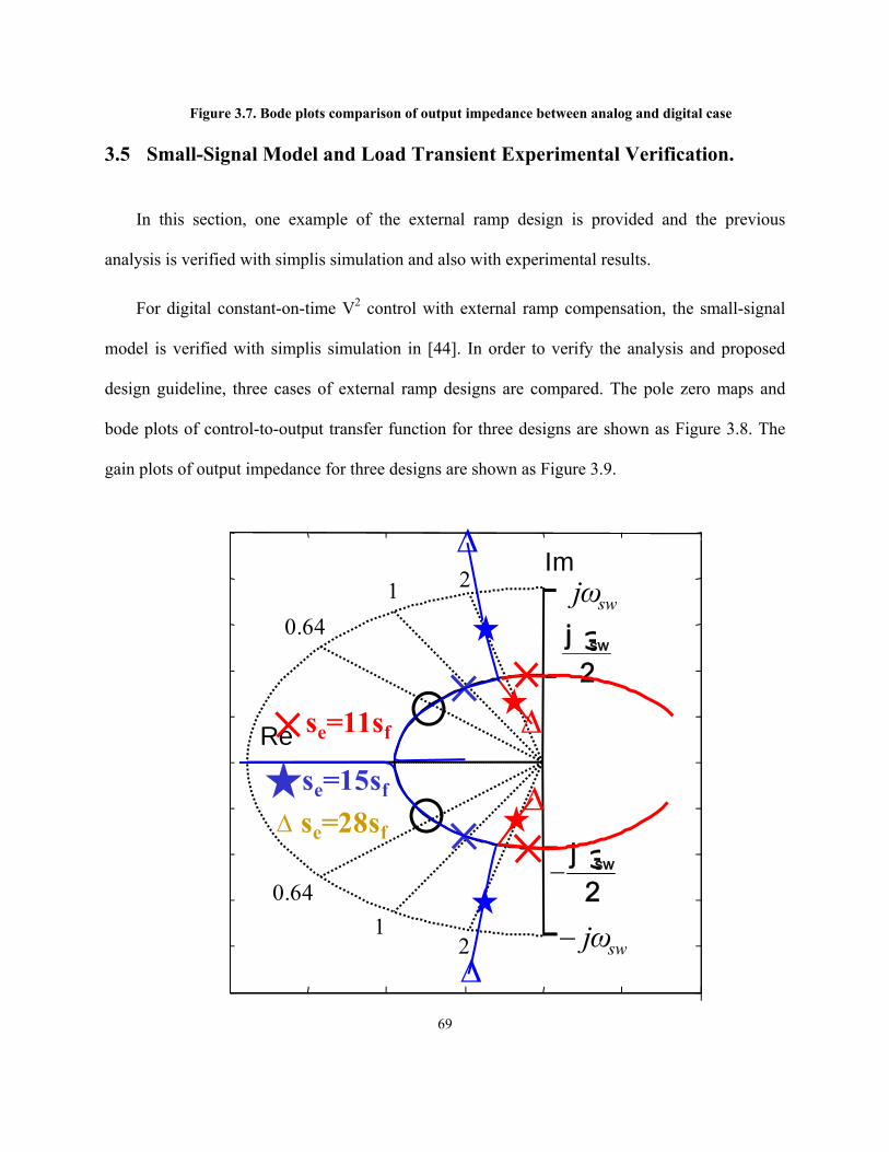
69
Figure 3.7. Bode plots comparison of output impedance between analog and digital case
3.5 Small-Signal Model and Load Transient Experimental Verification.
In this section, one example of the external ramp design is provided and the previous
analysis is verified with simplis simulation and also with experimental results.
For digital constant-on-time V2 control with external ramp compensation, the small-signal
model is verified with simplis simulation in [44]. In order to verify the analysis and proposed
design guideline, three cases of external ramp designs are compared. The pole zero maps and
bode plots of control-to-output transfer function for three designs are shown as Figure 3.8. The
gain plots of output impedance for three designs are shown as Figure 3.9.
9 . 4 2 e + 0 0 5
9 . 4 2 e + 0 0 5
0 . 7 5
0 . 5 0 . 2 5
0 . 7 5
0 . 5 0 . 2 5
21
0.64
21
0.64
Im
Re
2j ωsw
2j ωsw
swjω
swjω
∆
∆
∆
∆
∆
se=11sf
se=28sf
se=15sf
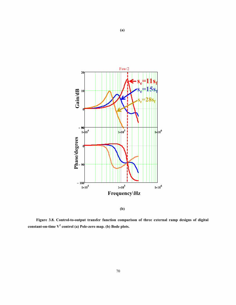
70
(a)
(b)
Figure 3.8. Control-to-output transfer function comparison of three external ramp designs of digital
constant-on-time V2 control (a) Pole-zero map. (b) Bode plots.
1 104 1 10
5 1 106
10
0
10
20
1 104 1 10
5 1 106
180
90
0
90
1 104 1 10
5 1 106
10
0
10
20
1 104 1 10
5 1 106
180
90
0
90
1 104 1 10
5 1 106
180
90
0
90
Gai
n/d
BP
has
e/d
egre
es
Frequency\Hz
Fsw/2
1 104 1 10
5 1 106
10
0
10
20
se=11sf
se=15sf
se=28sf
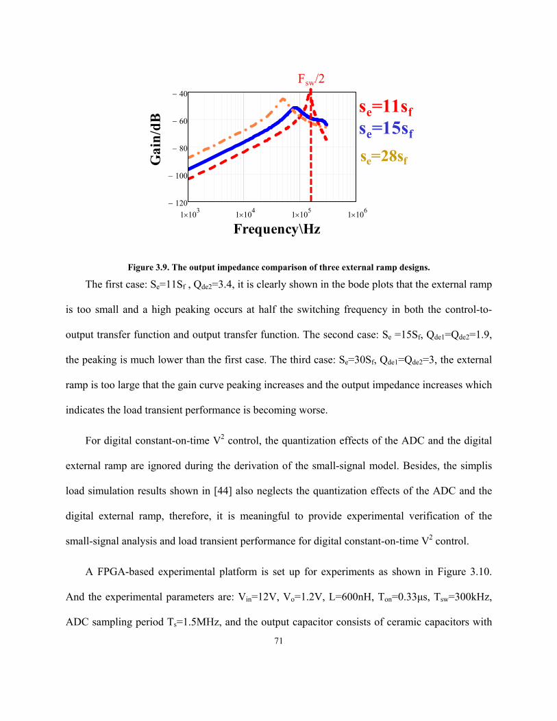
71
Figure 3.9. The output impedance comparison of three external ramp designs.
The first case: Se=11Sf , Qde2=3.4, it is clearly shown in the bode plots that the external ramp
is too small and a high peaking occurs at half the switching frequency in both the control-to-
output transfer function and output transfer function. The second case: Se =15Sf, Qde1=Qde2=1.9,
the peaking is much lower than the first case. The third case: Se=30Sf, Qde1=Qde2=3, the external
ramp is too large that the gain curve peaking increases and the output impedance increases which
indicates the load transient performance is becoming worse.
For digital constant-on-time V2 control, the quantization effects of the ADC and the digital
external ramp are ignored during the derivation of the small-signal model. Besides, the simplis
load simulation results shown in [44] also neglects the quantization effects of the ADC and the
digital external ramp, therefore, it is meaningful to provide experimental verification of the
small-signal analysis and load transient performance for digital constant-on-time V2 control.
A FPGA-based experimental platform is set up for experiments as shown in Figure 3.10.
And the experimental parameters are: Vin=12V, Vo=1.2V, L=600nH, Ton=0.33μs, Tsw=300kHz,
ADC sampling period Ts=1.5MHz, and the output capacitor consists of ceramic capacitors with
1 103 1 10
4 1 105 1 10
6120
100
80
60
40
Fsw/2
Gai
n/d
B
Frequency\Hz
se=11sf
se=15sf
se=28sf
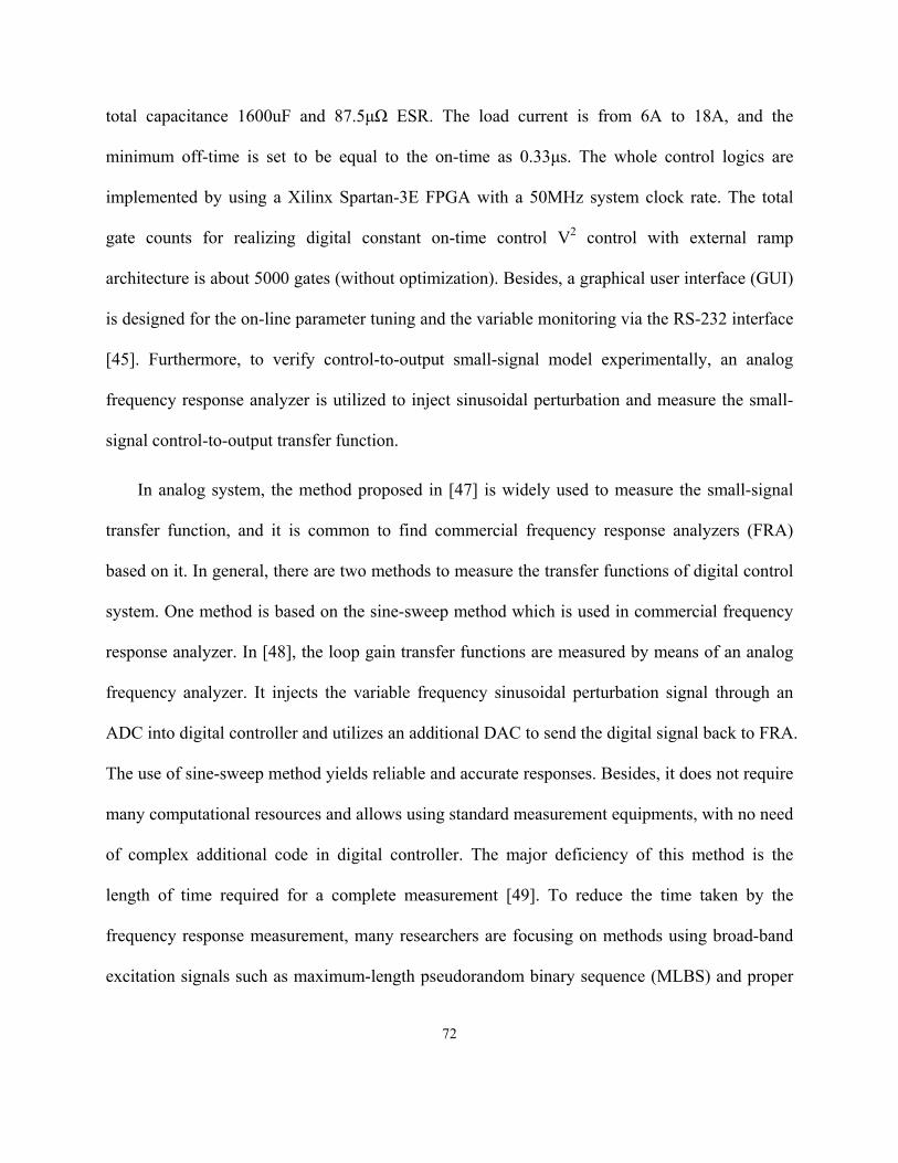
72
total capacitance 1600uF and 87.5μΩ ESR. The load current is from 6A to 18A, and the
minimum off-time is set to be equal to the on-time as 0.33μs. The whole control logics are
implemented by using a Xilinx Spartan-3E FPGA with a 50MHz system clock rate. The total
gate counts for realizing digital constant on-time control V2 control with external ramp
architecture is about 5000 gates (without optimization). Besides, a graphical user interface (GUI)
is designed for the on-line parameter tuning and the variable monitoring via the RS-232 interface
[45]. Furthermore, to verify control-to-output small-signal model experimentally, an analog
frequency response analyzer is utilized to inject sinusoidal perturbation and measure the small-
signal control-to-output transfer function.
In analog system, the method proposed in [47] is widely used to measure the small-signal
transfer function, and it is common to find commercial frequency response analyzers (FRA)
based on it. In general, there are two methods to measure the transfer functions of digital control
system. One method is based on the sine-sweep method which is used in commercial frequency
response analyzer. In [48], the loop gain transfer functions are measured by means of an analog
frequency analyzer. It injects the variable frequency sinusoidal perturbation signal through an
ADC into digital controller and utilizes an additional DAC to send the digital signal back to FRA.
The use of sine-sweep method yields reliable and accurate responses. Besides, it does not require
many computational resources and allows using standard measurement equipments, with no need
of complex additional code in digital controller. The major deficiency of this method is the
length of time required for a complete measurement [49]. To reduce the time taken by the
frequency response measurement, many researchers are focusing on methods using broad-band
excitation signals such as maximum-length pseudorandom binary sequence (MLBS) and proper
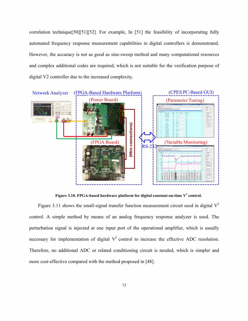
73
correlation technique[50][51][52]. For example, In [51] the feasibility of incorporating fully
automated frequency response measurement capabilities in digital controllers is demonstrated.
However, the accuracy is not as good as sine-sweep method and many computational resources
and complex additional codes are required, which is not suitable for the verification purpose of
digital V2 controller due to the increased complexity.
Figure 3.10. FPGA-based hardware platform for digital constant-on-time V2 control.
Figure 3.11 shows the small-signal transfer function measurement circuit used in digital V2
control. A simple method by means of an analog frequency response analyzer is used. The
perturbation signal is injected at one input port of the operational amplifier, which is usually
necessary for implementation of digital V2 control to increase the effective ADC resolution.
Therefore, no additional ADC or related conditioning circuit is needed, which is simpler and
more cost-effective compared with the method proposed in [48].
(Parameter Tuning)
(Variable Monitoring)RS-232
(CPES PC-Based GUI)(FPGA-Based Hardware Platform)
(Power Board)
(FPGA Board)
Network Analyzer
74
Figure 3.11. Small-signal control-to-output transfer function measurement circuit.
Figure 3.12 shows the measurement results for three different external ramp cases. The pole-
zero movements with different external ramps analyzed previously is verified and the case with
Se=15Sf is the best among the three curves. Figure 3.13 verify the small-signal model with the
experimental results with Se=15Sf case. The gain and phase curves agree with each other very
well up to half the switching frequency except that experimental phase curve shows around 15
deg more phase delay at high frequency. The high frequency phase difference is caused by the
additional delay in the implementation, mainly the driver delay (around 90ns) and the control
delay (around 60 ns). After adding the delay effect in the circuit, the phase discrepancy reduces
and the accuracy improves, which can be seen in Figure 3.13. (The black dotted line is the model
adding the delay term while the blue dashed line is the simulation results).
ADC sV
VinDriver 0.2
L1.4 / 16m
100 *16u
_err dv
erroK
DPWM
_o sv
Digital Ramp ds
_c newv
cv
Constant -on timeDPWM Digital
Comprefv
ov
rv
pv
rvpv ov
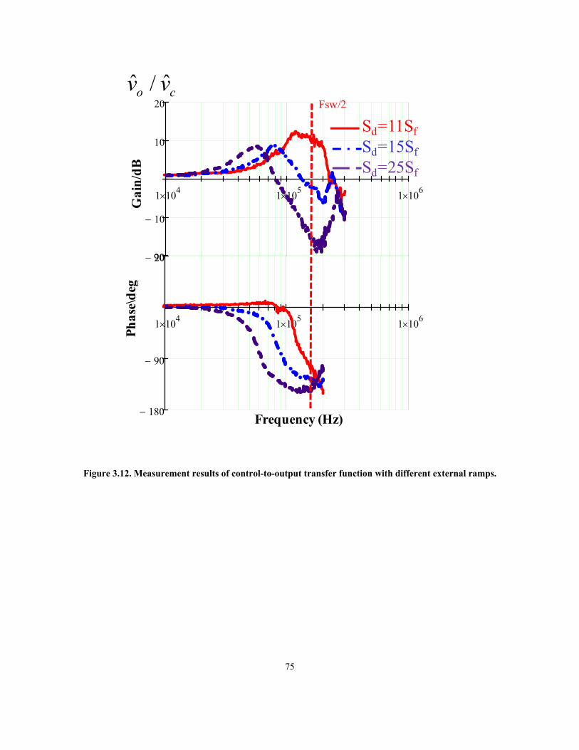
75
Figure 3.12. Measurement results of control-to-output transfer function with different external ramps.
1 104 1 10
5 1 106
180
90
90
1 104 1 10
5 1 106
20
10
10
20
ˆ ˆ/o cv v
Gai
n/d
BP
has
e\d
eg
Frequency (Hz)
Fsw/2
Sd=11Sf
Sd=15Sf
Sd=25Sf
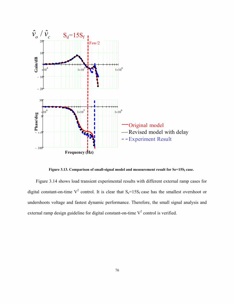
76
Figure 3.13. Comparison of small-signal model and measurement result for Se=15Sf case.
Figure 3.14 shows load transient experimental results with different external ramp cases for
digital constant-on-time V2 control. It is clear that Se=15Sf case has the smallest overshoot or
undershoots voltage and fastest dynamic performance. Therefore, the small signal analysis and
external ramp design guideline for digital constant-on-time V2 control is verified.
1 104 1 10
5 1 106
20
10
10
20
Gai
n/d
B
Fsw/2
1 104 1 10
5 1 106
180
110
40
30
Ph
ase\
deg
Frequency (Hz)
Sd=15Sfˆ ˆ/o cv v
Original model Revised model with delayExperiment Result
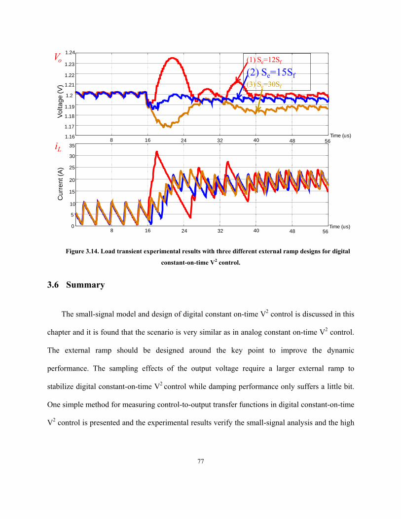
77
Figure 3.14. Load transient experimental results with three different external ramp designs for digital
constant-on-time V2 control.
3.6 Summary
The small-signal model and design of digital constant on-time V2 control is discussed in this
chapter and it is found that the scenario is very similar as in analog constant on-time V2 control.
The external ramp should be designed around the key point to improve the dynamic
performance. The sampling effects of the output voltage require a larger external ramp to
stabilize digital constant-on-time V2 control while damping performance only suffers a little bit.
One simple method for measuring control-to-output transfer functions in digital constant-on-time
V2 control is presented and the experimental results verify the small-signal analysis and the high
Vo
1.2
Vo
ltag
e (V
)
1.16
1.17
1.18
1.19
1.21
1.22
1.23
1.24
Time (us)8 16 24 32 40 48 56
iL
Time (us)8 16 24 32 40 48 56
0
5
10
15
Cu
rre
nt (
A) 25
35
20
30
(1) Se=12Sf
(2) Se=15Sf(3) Se=30Sf

78
frequency phase difference reveals the delay effects in the circuit. Load transient experimental
results prove the proposed design guideline for digital constant on-time V2 control.
79
Chapter 4. Summary and Future Work
4.1 Summary
Recently, constant-on-time V2 control is more and more popular in industry products due to
features of high light load efficiency, simple implementation and fast transient response. In many
applications such as cell phone, camera, and other portable devices, low-ESR capacitors such as
ceramic caps are preferred due to small size and small output voltage ripple requirement.
However, for the converters with ceramic caps, the conventional V2 control suffers from the sub-
harmonic oscillation due to the lagging phase of the capacitor voltage ripple relative to the
inductor current ripple. Two solutions to eliminate sub-harmonic oscillations are discussed in [39]
and the small-signal models are also derived based on time-domain describing function.
However, the characteristic of constant-on-time V2 with external ramp is not fully understood
and no explicit design guideline for the external ramp is provided. For digital constant on-time
V2 control, the high resolution PWM can be eliminated due to constant on-time modulation
scheme and direct output voltage feedback [43]. However, the external ramp design is not only
related to the amplitude of the limit-cycle oscillation, but also very important to the stability of
the system. The previous analysis is not thorough since numerical solution is used. The primary
objective of this work is to gain better understanding of the small-signal characteristic for analog
and digital constant-on-time V2 with ramp compensations, and provide the design guideline
based on the factorized small-signal model.

80
First, constant on-time current-mode control and constant on-time V2 control are reviewed.
Generally speaking, constant-on-time current mode control does not have stability issues.
However, for constant-on-time V2 control with ceramic caps, sub-harmonic oscillation occurs
due to the lagging phase of the capacitor voltage ripple. External ramp compensation and current
ramp compensation are two solutions to solve the problem. Previous equivalent circuit model
extended by Ray Ridley’s sample-and-hold concept is not applicable since it fails to consider the
influence of the capacitor voltage ripple. The model proposed in [39] successfully considers the
influence from the capacitor voltage ripple by using time-domain describing function method.
However, the characteristic of constant-on-time V2 with external ramp is not fully understood.
Therefore, more research focusing on the analysis is needed to gain better understanding of the
characteristic and provide the design guideline for the ramp compensations.
After that, the small-signal model and design of analog constant on-time V2 control is
investigated and discussed. The small-signal models are factorized and pole-zero movements are
identified. It is found that with increasing the external ramp, two pairs of double poles first move
toward each other at half of switching frequency, after meeting at the key point, the two double
poles separate, one pair moves to a lower frequency and the other moves to a higher frequency
while keeping the quality factor equal to each other. For output impedance, with increasing the
external ramp, the low frequency magnitude also increases. The recommended external ramp is
around two times the magnitude at the key point K. When Duty cycle is larger, the damping
performance is not good with only external ramp compensation, unless very high switching
frequency is used. With current ramp compensation, it is recommended to design the current
81
ramp so that the quality factor of the double pole is around 1. With current ramp compensation,
the damping can be well controlled regardless of the circuit parameters.
Next, the small-signal analysis and design strategy is also extended to digital constant on-
time V2 control structure which is proposed in [43]. It is found that the scenario is very similar as
analog constant on-time V2 control. The external ramp should be designed around the key point
to improve the dynamic performance. The sampling effects of the output voltage require a larger
external ramp to stabilize digital constant-on-time V2 control while suffers only a little bit of
damping performance. One simple method for measuring control-to-output transfer functions in
digital constant-on-time V2 control is presented. The experimental results verify the small-signal
analysis except for the high frequency phase difference which reveals the delay effects in the
circuit. Load transient experimental results prove the proposed design guideline for digital
constant on-time V2 control.
As a conclusion, the characteristics of analog and digital constant-on-time V2 control
structures are examined and design guidelines are proposed for ramp compensations based on the
factorized small-signal model. The analysis and design guideline are verified with simplis
simulation and experimental results.
4.2 Future Work
Although small-signal model based on the describing function method is very accurate. The
process is complicated and it needs start over-again when deriving different transfer function or
using different topologies. Equivalent circuit model can be a good way to understand the
complicated small-signal behavior. Right now, there is no equivalent circuit model considering

82
the influence from the capacitor voltage ripple and therefore no equivalent circuit model for V2
control with ceramic caps. Although it is very difficult, it is still possible to get an equivalent
circuit model for V2 control using ceramic caps.
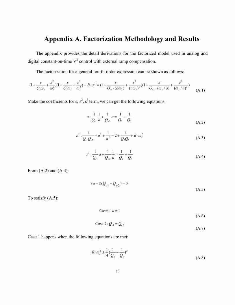
83
Appendix A. Factorization Methodology and Results
The appendix provides the detail derivations for the factorized model used in analog and
digital constant-on-time V2 control with external ramp compensation.
The factorization for a general fourth-order expression can be shown as follows:
))/()/(
1)()()(
1()1)(1(2
2
2
222
2
2
21
222
2
2322
2
22 a
s
aQ
s
a
s
aQ
ssB
s
Q
ss
Q
s
ee
(A.1)
Make the coefficients for s, s2, s3 term, we can get the following equations:
3221
11111:
QQa
QaQs
ee
(A.2)
22
322
2
21
2 12
11: B
QQaa
QQs
ee
(A.3)
3221
3 11111:
QQaQa
Qs
ee
(A.4)
From (A.2) and (A.4):
0)21
)(1( e
Qe
Qa (A.5)
To satisfy (A.5):
1:1 aCase (A.6)
21:2 ee QQCase (A.7)
Case 1 happens when the following equations are met:
2
32
22 )
11(
4
1
QQB
(A.8)
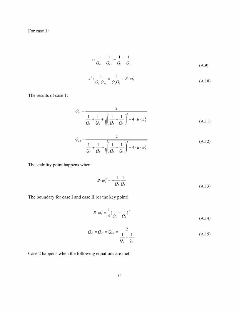
84
For case 1:
3221
1111:
QQQQs
ee
(A.9)
22
3221
2 11: B
QQQQs
ee
(A.10)
The results of case 1:
22
2
3232
1
41111
2
BQQQQ
Qe
(A.11)
22
2
3232
2
41111
2
BQQQQ
Qe
(A.12)
The stability point happens when:
32
22
11
QQB
(A.13)
The boundary for case I and case II (or the key point):
2
32
22 )
11(
4
1
QQB
(A.14)
32
21 112
QQQ eKee
(A.15)
Case 2 happens when the following equations are met:
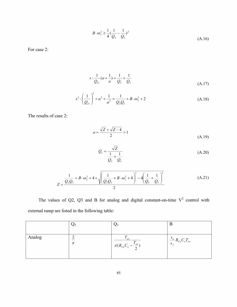
85
2
32
22 )
11(
4
1
QQB
(A.16)
For case 2:
321
11)
1(
1:
QQaa
Qs
e
(A.17)
2111
: 22
322
2
2
1
2
B
QQaa
Qs
e
(A.18)
The results of case 2:
12
4
ZZa
(A.19)
32
11
ZQe
(A.20)
2
1144
14
12
32
2
22
32
22
32
BQQ
BQQ
Z
(A.21)
The values of Q2, Q3 and B for analog and digital constant-on-time V2 control with
external ramp are listed in the following table:
Q2 Q3 B
Analog 2
)2
( onoCo
sw
TCR
T
swoCo
f
e TCRs
s

86
Digital 2
))int(2
( ss
offonoCo
sw
TT
TTCR
T
swoCo
f
e TCRs
s
Substituting these values, the results shown in section 2.2 and 3.2 can be derived.
87
Reference
[1] L. E. Galllaher, “Current Regulator with AC and DC Feedback,” U.S. Patent 3,350,628,
1967.
[2] F. C. Schwarz, “Analog Signal to Discrete Time Interval Converter (ASDTIC),” U. S.
Patent 3,659,184, 1972.
[3] A. D. Schoenfeld, Y. Yu, “ASDTIC Control and Standardized Interface Circuits Applied
to Buck, Parallel and Buck-Boost DC-to-DC Power Converters,” NASA Report NASA
CR-121106, February, 1973.
[4] P. L. Hunter, “Converter Circuit and Method Having Fast Responding Current Balance and
Limiting,” U.S. Patent 4,002,963, 1977.
[5] A. Capel, G. Ferrante, D. O’Sullivan, and A. Weinberg, “Application of the Injected
Current Model for the Dynamic Analysis of Switching Regulators with the New Concept
of LC3 Modulator,” in proc. IEEE PESC’78, pp. 135-147.
[6] C. W. Deisch, “Switching Control Method Changes Power Converter into a Current
Source,” in proc. IEEE PESC’78, pp. 300-306.
[7] R. Redl and N. O. Sokal, “Current-mode control, five different types, used with the three
basic classes of power converters: small-signal ac and large-signal dc characterization,
stability requirements, and implementation of practical circuits,” in Proc. IEEE PESC’85,
pp. 771-785.
[8] L.H. Dixon, “Average Current-Mode Control of Switching Power Supplies,” Unitrode
Power Supply Design Seminar handbook, 1990, pp. 5.1-5.14
[9] W.Tang, Y.Jiang, G.C.Hua, F.C.Lee, I.Cohen, “Power Factor Correction With Flyback
Converter Employing Charge Control” in Proc. IEEE APEC’93, pp. 293 – 298, 1993.
[10] I. Cohen, “Adaptive control method for power converters,” U. S. Patent 5,438,505, 1995.
88
[11] Analog Devices, ADP2102 datasheet, http://www.analog.com/static/imported-
files/data_sheets/ADP2102.pdf.
[12] Linear Technology, LTC3709 datasheet, www.linear.com/docs/6026
[13] Maxim, MAX1545 datasheet, http://datasheets.maxim-ic.com/en/ds/MAX1519-
MAX1545.pdf.
[14] National Semiconductor, LM34919 datasheet, http://www.national.com/ds/LM/
LM34919.pdf.
[15] Texas Instruments, TPS51116 datasheet, http://focus.ti.com/lit/ds/symlink/ tps51116.pdf.
[16] STMicroelectronics, PM6685 data sheet, http://www.st.com/stonline/products/
literature/ds/11674/pm6685.pdf.
[17] Intersil, ISL6237 data sheet, www.intersil.com/data/fn/fn6418.pdf.
[18] Shi-Ping Hsu, A. Brown, L. Rensink, R. Middlebrook, “Modeling and analysis of
switching dc to dc converters in constant frequency current programmed mode,” PESC 79
Record, pp 284-301
[19] F.C. Lee, Y. Yu, and M.F. Mahmoud, “A Unified Analysis and Design Procedure for a
Standardized Control Module for DC-DC Switching Regulators, ” in proc. IEEE PESC’80,
pp.284-301.
[20] R. D. Middlebrook, “Topics in Multiple-Loop Regulators and Current Mode
Programming,” in proc. IEEE PESC’85, pp. 716-732
[21] R.D. Middlebrook, “Modeling Current-Programmed Buck and Boost Regulators,” IEEE
Trans. Power Electron., Vol. 4, pp. 36-52, January 1989.
[22] D. J. Packard, “Discrete Modeling and Analysis of Switching Regulators,” Ph.D.
dissertation, Cal. Tech., CA, May 1976.
[23] A. R. Brown and R. D. Middlebrook, “Sample-Data Modeling of Switched Regulators,” in
proc. IEEE PESC’81, pp. 349-369.
89
[24] G. C. Verghese, C. A. Bruzos, and K. N. Mahabir, “Averaged and sample-data models for
current mode control: A reexamination,” in Proc. IEEE PESC’89, pp. 484-491.
[25] R. Redl, “High-frequency extension of the small-signal model of the constant-frequency
current-mode-controlled converter,” in proc. IEEE APEC '91, pp. 466 – 472.
[26] R. B. Ridley, “A new, continuous-time model for current-mode control,” IEEE Trans.
Power Electron., vol. 6, no. 2, pp. 271-280, April 1991.
[27] F. D. Tan and R. D. Middlebrook, “A unfied model for current-programmed converters,”
IEEE Trans. Power Electron., vol. 10, no. 4, pp.397–408, Jul. 1995.
[28] R. B. Ridley, “A new continuous-time model for current-mode control with constant
frequency, constant on-time, and constant off-time, in CCM and DCM,” in proc. IEEE
PESC’90, pp. 382- 389.
[29] Jian Li, Fred C. Lee, “New modeling approach and equivalent circuit representation for
current mode control” IEEE Trans. Power Electron., vol. 25, no. 5, pp.1218–1230, May.
2010.
[30] D. Goder and W. R. Pelletier, “V2 architecture provides ultra-fast transient response in
switch mode power supplies," in proc. HFPC’96, pp. 19-23.
[31] D. Goder, “Switching regulators,” U.S. Patent, 5,770,940, 1998.
[32] J. Sun, “Characterization and performance comparison of ripple based control for voltage
regulator modules,” IEEE Trans. Power Electron., vol. 21, no. 2, pp. 346-353, Mar. 2006.
[33] R. Redl and J. Sun, “Ripple-based control of switching regulators –an overview,” IEEE
Trans. Power Electron., vol. 24, no. 12, pp.2669-2680, Dec. 2009.
[34] W. Huang and J. Clarkin, “Analysis and design of multiphase synchronous buck converter
with enhanced V2 control,” in Proc. HFPC,2000, pp. 74–81.
[35] W. Huang, “A new control for multi-phase buck converter with fast transient response,” in
Proc. IEEE APEC, Anaheim, CA, 2001, pp.273–279.
[36] S. Qu, “Modeling and design considerations of V2 controlled buck regulator,” in Proc.
IEEE APEC, Anaheim, CA, 2001, pp. 507–513.
90
[37] J. Sun, “Characterization and performance comparison of ripple-based control for voltage
regulator modules,” IEEE Trans. Power Electron.,vol. 21, no. 2, pp. 346–353, Mar. 2006.
[38] R. Redl and J. Sun, “Ripple-based control of switching regulators –an overview,” IEEE
Trans. Power Electron., vol. 24, no. 12, pp.2669-2680, Dec. 2009.
[39] J. Li and F. C. Lee, “Modeling of V2 current-mode control,” in IEEE Tran .Circuits and
Systems, Part I, Vol. 57, No 9. Sep.2009, pp. 2552-2563.
[40] Y. F. Liu, E. Meyer, and X. D. Liu, “Recent developments in digital control strategies for
DC/DC switching power converters,” IEEE Trans. Power Electron., vol. 24, no. 11, pp.
2567-2577, Nov. 2009.
[41] A. V. Peterchev and S. R. Sanders, “Quantization resolution and limit cycling in digitally
controlled PWM converters”, IEEE Trans. Power Electron., vol. 18, pp. 301-308, Jan.
2003.
[42] H. Peng, A. Prodic, E. Alarcon, and D. Maksimovic, "Modeling of quantization effects in
digitally controlled dc-dc converters," in Proc. IEEE PESC’04, Aachen, Germany, pp.
4312-4318.
[43] J. Li and F. C. Lee, “Digital current mode control architecture with improved performance
for DC-DC converters,” in Proc. IEEE APEC, 2008, pp. 1087-1092.
[44] J. Li, “Current-mode control: modeling and its digital application,” Ph. D. Dissertation,
Virginia Tech, April, 2009. pp. 121-130.
[45] K. Y. Cheng, F. Yu, P. Mattavelli, and F. C. Lee, “Characterization and performance
comparison of digital V2-type constant on-time control for buck converters,” in Proc.
IEEE COMPEL Conf., 2010.
[46] T. Qian W. Wu, “Analysis of the ramp compensation approaches to improve stability for
buck converters with constant-on-time control,” in IET Power Electronics .Vol 5, Issue 2.
2012.pp.196-204
[47] R. Middlebrook, “Measurement of loop gain in feedback systems,” Int. J.Electron., vol. 38,
no. 4, pp. 485–512, Apr. 1975.
91
[48] F. G. Espín, E.Figueres, G. Garcera, R.G.Medina, M. Pascual “Measurement of the Loop
Gain Frequency Response of Digitally Controlled Power Converters,” IEEE Trans.
Industrial Electronics, vol. 57, no. 8, pp. 2785-2796, Aug. 2010.
[49] T.Roinila, M.Vilkko, T.Suntio."Frequency-Response Measurement of Switched-Mode
Power Supplies in the Presence of Nonlinear Distortions", IEEE Trans. Power Electronics,
vol. 25, no. 8,pp2179-2187.Aug.2010.
[50] B. Miao, R. Zane, and D. Maksimovic, “A modified cross-correlation method for system
identification of power converters with digital control,”in Proc. IEEE Power Electron.
Spec. Conf., 2004, pp. 3728–3733.
[51] M. Shirazi, J. Morroni, A.Dorgov, K. Zane and D. maksimovic, "Integration of frequency
response measurement capabilities in digital controllers for dc-dc converters," IEEE Trans.
Power Electronics, vol.23, no. 5, pp. 2524-2535, Sep. 2008.
[52] A. Barkley and E. Santi, “Improved online identification of switching converters using
digital network analyzer techniques,” in Proc. IEEE PowerElectron. Spec. Conf., 2008, pp.
891–896.