Embed Size (px)
Citation preview

International Journal of Engineering Trends and Technology (IJETT) – Volume-44 Number-2 -February 2017
ISSN: 2231-5381 http://www.ijettjournal.org Page 78
Small Scale Two Level PWM Driver Design
for Single Phase Sine Wave Inverter and Total
Harmonic Distortion Mitigation Mohammad Kamruzzaman Khan Prince1, Md. ZahedIqbal2, Mohammed AbrarFahim3
1Faculty, Dept. of EEE, Shahjalal University of Science and Technology, Kumargaon, Sylhet-3114, Bangladesh 2Student, Dept. of EEE, Shahjalal University of Science and Technology, Kumargaon, Sylhet-3114, Bangladesh 3Student, Dept. of EEE, Shahjalal University of Science and Technology, Kumargaon, Sylhet-3114, Bangladesh
Abstract
Inverter is necessary for DC to AC conversion for
uninterrupted AC power supply and utilization of
many types of AC electrical equipment in our day to
day life. Square wave inverter and modified sine
wave (actually a cascaded square wave) inverter is
available which includes total harmonic distortion
(THD). In fact the generation of a pure sinusoidal
AC voltage is a big challenge with minimum amount
of total harmonic distortion. This paper deals with
the design of a project which is the hardware
implementation of a two level PWM driver to
achieve close approximated sinusoidal waveform for
DC to AC conversion with low harmonic distortion
in unloaded condition.
Keywords
Inverter, DC to AC Conversion, Total Harmonic
Distortion (THD), Pulse Width Modulation (PWM)
I. INTRODUCTION
An inverter is a DC to AC converter. In real life,
for numerous applications DC to AC conversion is
required. Uninterruptible Power Supply (UPS), AC
motor drives, grid-connected wind energy or
photovoltaic system are few of such fields where
inverter is widely used.
At present three types of single phase inverters
are available in the market. These are
1. Square wave inverter
2. Modified sine wave inverter
3. Pure sine wave inverter
Among those square wave inverter and modified
sine wave inverter suffers from high harmonic
contents. These are inefficient and not suitable for a
large number of applications like clock and timers.
But pure sine wave inverter provides output very
close to the output generated by an AC generator.
Inverter can also be classified as voltage source
inverter (VSI) where the output is AC voltage and as
current source inverter (CSI) where the output is AC
current.
Common topologies used by an inverter are half
bridge and full bridge topologies in conjunction with
Pulse Width Modulation (PWM) switching schemes.
Three basic PWM techniques are available-
1. Single pulse width modulation
2. Multiple pulse width modulation
3. Sinusoidal pulse width modulation
This paper deals with a VSI type pure sine wave
inverter in conjunction with analog sinusoidal PWM
techniques implemented by half bridge topology.
II.OBJECTIVES Our aim is to design a close approximation of
pure sine wave with low total harmonic distortion on
no load condition.
III. SOFTWARE USED
TINA-TI is simulator software of Texas Instrument.
Tina90-TIen.9.3.150.4 version is used for
simulation.
IV. SINGLE PHASE HALF BRIDGE PURE
SINE WAVE INVERTER
From Fig. 1 it is clear that, two semiconductor
switches are employed with freewheeling diodes. By
operating these switches simultaneously using PWM
technique, desired AC output is generated.
Fig.1Half bridge inverter topology
As switch BJT, Thyristor, IGBT, MOSFET etc. can
be used. In our project MOSFET switches have been
used due to the following advantages-
1. MOSFET contains an anti-parallel Schoktty
diode
2. Fast switching characteristics
3. High efficiency
International Journal of Engineering Trends and Technology (IJETT) – Volume-44 Number-2 -February 2017
ISSN: 2231-5381 http://www.ijettjournal.org Page 79
V. SINUSOIDAL PULSE WIDTH
MODULATION (SPWM) TECHNIQUE
This type of control generates constant amplitude
pulses by modulating the pulse duration by varying
duty cycle. Here a reference sine wave with desired
AC output frequency and a high frequency triangular
or saw tooth carrier wave is compared using a
comparator circuit.
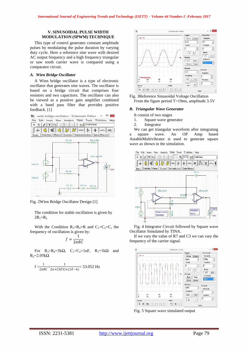
A. Wien Bridge Oscillator
A Wien bridge oscillator is a type of electronic
oscillator that generates sine waves. The oscillator is
based on a bridge circuit that comprises four
resistors and two capacitors. The oscillator can also
be viewed as a positive gain amplifier combined
with a band pass filter that provides positive
feedback. [1]
Fig. 2Wien Bridge Oscillator Design [1]
The condition for stable oscillation is given by
2R1=R2
With the Condition R3=R4=R and C1=C2=C, the
frequency of oscillation is given by:
𝑓 =1
2𝜋𝑅𝐶
For R3=R4=3kΩ, C1=C2=1uF, R1=1kΩ and
R2=2.05kΩ
f =1
2𝜋𝑅𝐶=
1
2𝜋× 3𝐸3 ×(1𝐸−6)= 53.052 Hz
Fig. 3Reference Sinusoidal Voltage Oscillation
From the figure period T=19ms, amplitude 3.5V
B. Triangular Wave Generator
It consist of two stages
1. Square wave generator
2. Integrator
We can get triangular waveform after integrating
a square wave. An OP Amp based
AstableMultivibrator is used to generate square
wave as shown in the simulation.
Fig. 4 Integrator Circuit followed by Square wave
Oscillator Simulated by TINA.
If we vary the value of R7 and C3 we can vary the
frequency of the carrier signal.
Fig. 5 Square wave simulated output

International Journal of Engineering Trends and Technology (IJETT) – Volume-44 Number-2 -February 2017
ISSN: 2231-5381 http://www.ijettjournal.org Page 80
Fig. 6 Triangular carrier wave after the integration
of square wave
C. Comparator Circuit: Basic PWM Gate Pulse
Generation
We have designed a comparator circuit by op amp
where Vin is the carrier triangular wave and Vref is
the sine 50-60 Hz oscillation wave.
After comparision of this two signals output gives
us PWM signal which can be used as gate pulse.
Fig. 7 Compared PWM output where, Vref is
modulating sine wave oscillation and Vin is carrier
Triangular wave [2]
D. Complete Design of PWM Driver Circuit
By assembling wein bridge oscillator, triangular
wave generator and comparator circuit the complete
PWM driver circuit is built which is shown in Fig. 8
below.
Fig. 8 PWM driver circuit schematic design
VI.INVERTING AMPLIFIER AND BUFFER
CIRCUIT
Inverting amplifier is used for gain maintaining of
sine wave from attenuation. Another inverting
amplifier is used for the generation of
complimentary PWM gate pulse [1].
Fig. 9 Inverting Amplifier and Buffer circuit
schematic by TINA.
Where, Vout = - Vin (R2/R1)
When R2=R1
Then Vout = - Vin
Voltage follower mitigates the distortion of a
voltage from loading effect.Here it works as a
perfect voltage source.It saves Op-Amp from
bruning out in loading condition.
Where Vin=Vout
Two buffer circuits are practically implemented
after two PWM gate pulse circuit. Buffer circuit is
also used after sine wave oscillator circuit and
carrier wave circuit although buffer circuit is
withdrawn from schematic design here.
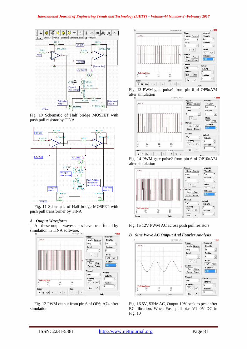
VII.APPLICATION OF PWM TECHNIQUE TO
HALF BRIDGE SINE WAVE INVERTER
It consists of PWM gate pulse circuit from where
gate pulses are applied in the gate pin of two
MOSFETs. In this case push pull technique is
applied in the drain terminal by two low valued
resistances. Second order low pass RC filter is used
across the push pull resistors (R12 and R13) to get
smooth sinusoidal AC voltage.
International Journal of Engineering Trends and Technology (IJETT) – Volume-44 Number-2 -February 2017
ISSN: 2231-5381 http://www.ijettjournal.org Page 81
Fig. 10 Schematic of Half bridge MOSFET with
push pull resistor by TINA.
Fig. 11 Schematic of Half bridge MOSFET with
push pull transformer by TINA
A. Output Waveform
All these output waveshapes have been found by
simulation in TINA software.
Fig. 12 PWM output from pin 6 of OP6uA74 after
simulation
Fig. 13 PWM gate pulse1 from pin 6 of OP9uA74
after simulation
Fig. 14 PWM gate pulse2 from pin 6 of OP10uA74
after simulation
Fig. 15 12V PWM AC across push pull resistors
B. Sine Wave AC Output And Fourier Analysis
Fig. 16 5V, 53Hz AC, Output 10V peak to peak after
RC filtration, When Push pull bias V1=0V DC in
Fig. 10

International Journal of Engineering Trends and Technology (IJETT) – Volume-44 Number-2 -February 2017
ISSN: 2231-5381 http://www.ijettjournal.org Page 82
Fig. 17 10V, 53Hz sine AC, Output 20V peak to
peak after RC filtration, When Push pull Bias
V1=12V DC in Fig. 10
Fig. 18 110V AC when Push Pull bias voltage
V1=0V DC in Fig. 11
Fig. 19 220V AC when Push Pull bias voltage
V1=12V DCin Fig. 11
TABLE I
FOURIER COEFFICIENTS OF SINE
WAVE AC BY TINA SOFTWARE
Output is 110V AC with carrier frequency of 8kHz.
Amplitude and phase versus frequency plotof
Fourier coefficients is shown below.
Fig. 20 Amplitude and phase versus frequency
plot of Fouriercoefficients, for fc=8 kHz
VIII. HARDWARE IMPLEMENTATION
DC source: Two 6V and two 12V Lead Acid
Battery.
Resistors: 680,1K,10K,12K,22K,100K, 10K
(variable) Ohm resistors.
Capacitors: 10nF,0.47uF,1uF
Op-Amp IC: LM324N
MOSFETS: IRF630N N channel

International Journal of Engineering Trends and Technology (IJETT) – Volume-44 Number-2 -February 2017
ISSN: 2231-5381 http://www.ijettjournal.org Page 83
Fig. 21 Quad Op-Amp IC LM324N datasheet [3]
Fig. 22 N channel IRF 630N MOSFET Datasheet [4]
Fig. 23 Hardware Implementation of ICs
A. Circuit output waveform in Oscilloscope
Fig. 24 Reference 53Hz sine wave form Wien
Bridge Oscillator circuit.
Fig. 25 Carrier triangular wave form
Fig. 26 PWM Wave shape
Fig. 27 Filtered 53Hz, 10V AC output from
MOSFET-Push pull Network.

International Journal of Engineering Trends and Technology (IJETT) – Volume-44 Number-2 -February 2017
ISSN: 2231-5381 http://www.ijettjournal.org Page 84
B. AC Wave shape Quality: A Comparison
TABLE III
TOTAL HARMONIC DISTORTION
(THD) OF THE SIGNAL
CALCULATED BY TINA TI.
Base frequency, fsin=50Hz
Two levels PWM circuit (No load condition)
Carrier
freque
nc-y fc
(Appr
oxi-
mated)
Modulat
i-on
Index
m=fc/fsi
n
Resista-
nce
value R7
for
variable
fc
THD
for
10V
AC
THD
for
110V
AC
500 10 1.75kΩ 66.54% 46.00%
750 15 1.17kΩ 58.12% 58.48%
1000 20 1.09kΩ 64.31% 53.92%
1250 25 900Ω 59.45% 57.17%
1500 30 640Ω 69.54% 68.69%
2000 40 500Ω 54.59% 64.89%
4000 80 300Ω 55.68% 45.16%
5700 114 149Ω 70.44% 24.45%
8000 160 120Ω 56.27% 13.09%
IX. DISCUSSION
From our implemented sine wave inverter,
sinusoidal AC voltage has been found which has less
harmonic distortion. However this sine wave AC
output voltage includes 1.5V average ripple content.
Wien bridge oscillator is practically implemented for
carrier wave generation for better triangular wave
shape. From the circuit we’ve designed THD is
minimized to 13% by using much higher 8kHz
carrier signal. The output voltage is stepped up when
more push-pull bias voltage is used. For example,
with push-pull bias voltage 0V output is 5V AC
(10V peak to peak) but with push-pull bias voltage
12V output is 10V AC (20V peak to peak). 2V DC is
lost.
X. FUTURE WORK
1. Design a feedback control system to
improve the capability of PWM diver for effective
implementation on inverter.
2. Hardware design of multi carrier based
PWM driver to implement multilevel inverter,
achieving less total harmonic distortion.
3. Improve the load capacity of the inverter.
XI. CONCLUSION
The simulated two levels PWM driver circuit is
designed successfully and implemented in hardware
project. The sinusoidal wave shape has been
achieved (no load) with minimum total harmonic
distortion and ripple. Transformer impedance
matching and feedback control system design is
necessary for the PWM driver to be effectively
implemented in inverter. Total harmonic distortion
(THD) in AC voltage would be mitigated much
more when high frequency (more than 8 kHz) carrier
signal would be used in the implemented circuit.
REFERENCES
[1] Electronics - Circuits and Systems by Woen Bishop, (4th
Edition) chapter 11, 12 and 14
[2] “Design and performance comparison of Two-level and
Multilevel Converters for HVDC Applications” by CARLOS
CASTILLO, BONILLASHWETA, MERILYN TIGGA,
Department of Energy and Environment, Division of Electric
Power Engineering, Sweden, year published 2011
[3] Quad OpAmp IC LM324N datasheet
[4] N channel IRF 630N MOSFET Datasheet by New Jersy
Semiconductors Inc.
[5] Power Electronics by M H Rashid, Third Edition Chapter 6
[6] Donald Fink (ed), Electronics Engineers' Handbook, McGraw
Hill, 1975 ISBN 0-07-020980-4, page 16-40
[7] “Analysis and Simulation of Cascaded H-Bridge Multi Level
Inverter Using Level-Shift PWM Technique” by Abhishek Kumar
Ranjan, D.VijayaBhaskar, Nibeditaparida. International
Conference on Circuit, Power and Computing Technologies
[ICCPCT], 2015
[8] “Inverter Control using output feedback for power
compensating devices” by A.Ghosh, A.K Jindal, A.Joshi,
Conference on Conergent Technologies for Asia Pasific Region,
publisher IEEE, TENCON Oct 2003