Embed Size (px)
Citation preview

Seiko Instruments Inc. 1
S-8323/8327 SeriesSMALL PACKAGE PWM CONTROL
STEP-UP SWITCHING REGULATOR
The S-8323/8327 Series is a CMOS PWM-control step-up switchingregulator which mainly consists of a reference voltage source, anoscillation circuit, a power MOS FET (for S-8323 Series) , and an erroramplifier. Equipped with best-designed control circuits, the productsmaintain high efficiency over a wide range of conditions with thecapability of automatically controlling the duty ratio from 0% to 83%(78% for 250kHz model) according to each applied load. A step-upswitching regulator is constructed by externally connecting only a coil, acapacitor and a diode to the S-8323 Series. This feature, along with itssmall package and low current consumption, makes the S-8323 Seriesideal for the power supply of portable equipment. For applicationsrequiring a high output current, products used with an external transistor(S-8327 Series) are also available.
n n Features
• Low voltage operation:0.9V(IOUT=1mA, 50kHz and 100kHz models)
• Low current consumption :During operation: 17.2µA (typ.)
(VOUT = 3 V, 50 kHz)During shutdown: 0.5µA (max.)
• Duty ratio: Built-in PWM control circuit
• External parts: coil, diode, and capacitor only(a transistor is needed for the S-8327 Series.)
• Output voltage: accuracy of ±2.4%
• Oscillation frequency: 30kHz, 50kHz, 100kHz, and250kHz
• Software start function is built-in
• Shutdown function
• External transistor type is available (S-8327 Series)
• SOT-23-5 small plastic package
• SOT-23-3 small plastic package
• SOT-89-3 miniature power molded plastic package
• Step-down and voltage-inverting type are available.
n n Applications
• Power supplies for portable equipment such as pagers, handy calculators, and remote controllers
• Constant voltage power supplies for cameras, video equipment, and communications equipment
• Power supply for microcomputers
n n Block Diagram
ON/ OFF
PWMcontrolcircuit
-+
VOUT
VOUTVOUT
VOUT
CONT
CONT
VREF
Soft start circuit
VSS
-+
VREF
VSS
VDDVDD
VSS
VSS
-+
VREF
-+
VREF
EXT
EXT
ON/ OFF
(2) S-8327 Series (Types B, H)(1) S-8323 Series (Types A, C, H)
PWMcontrolcircuit
Soft start circuit
(4) S-8327 Series (Types E, J)(3) S-8323 Series (Types D, J)
PWMcontrolcircuit
Soft start circuit
PWMcontrolcircuit
Soft start circuit
Figure 1 Block Diagram
Rev. 7.1

SMALL PACKAGE PWM CONTROL STEP-UP SWITCHING REGULATORS-8323/8327 Series Rev. 7.1
2 Seiko Instruments Inc.
n n Selection Guide
1. Product NameS-832 X X XX XX - XXX - T2
Tape Specification
Product name (abbreviation)
Package name (abbreviation)MA : SOT-23-3 (without shutdown function)MC : SOT-23-5 (with shutdown function, VDD/VOUT separate product)UA : SOT-89-3 (without shutdown function)
Output voltage x 10
Product categoryA : Normal product, fosc=50 kHz (S-8323 only)B : Normal product, fosc=100 kHz (S-8327 only)C : For pagers, fosc=30 kHz (S-8323 only)D : VDD/VOUT separate product, fosc=50 kHz (S-8323 only)E : VDD/VOUT separate product, fosc=100 kHz (S-8327 only)H : Normal product, fosc=250 kHz (S-8323/7)J : VDD/VOUT separate product, fosc=250 kHz (S-8323/7)
Power transistor3: Built-in switch.7: External transistor.
2. Function List
Product NameBuilt In power
transistorwith external
powertransistor
Switchingfrequency
(kHz)
shutdownfunction
VDD/VOUT
separatetype
Package Application Referencepage
S-8323AXXMC Yes 50 Yes SOT-23-5 With shutdown function S-8323AXXMA Yes 50 SOT-23-3 Without shutdown function S-8323AXXUA Yes 50 SOT-89-3 Without shutdown function S-8323DXXMC Yes 50 Yes SOT-23-5 For variable output voltage by
step-up DC/DC converter andstep-down, inverted output DC/DCconverter with an external resistor
Page 20
S-8323CXXMA Yes 30 SOT-23-3 For pagers S-8323HXXMC Yes 250 Yes SOT-23-5 With shutdown function S-8323JXXMC Yes 250 Yes SOT-23-5 For variable output voltage by
step-up DC/DC converter andstep-down, inverted output DC/DCconverter with an external resistor
Page 20
S-8327BXXMC Yes 100 Yes SOT-23-5For large load current withshutdown function
Pages 19
S-8327BXXMA Yes 100 SOT-23-3For large load current withoutshutdown function
Pages 19
S-8327BXXUA Yes 100 SOT-89-3For large load current withoutshutdown function
Pages 19
S-8327EXXMC Yes 100 Yes SOT-23-5For variable output voltage bystep-up DC/DC converter with anexternal resistor
Pages 19 and20
S-8327HXXMC Yes 250 Yes SOT-23-5 For large load current withoutshutdown function
Pages 19
S-8327JXXMC Yes 250 Yes SOT-23-5 For variable output voltage bystep-up DC/DC converter with anexternal resistor
Pages 19 and20

SMALL PACKAGE PWM CONTROL STEP-UP SWITCHING REGULATORRev. 7.1 S-8323/8327 Series
Seiko Instruments Inc. 3
3. Product list
Output voltage(V)
S-8323AXXMCSeries
S-8323AXXMASeries
S-8323AXXUASeries
S-8323CXXMASeries
S-8323DXXMCSeries
2.0 S-8323D20MC-EZA-T22.5 S-8323A25MC-ELF-T2 S-8323A25MA-ELF-T2 S-8323A25UA-ELF-T2 S-8323C25MA-ENF-T2 2.7 S-8323A27MC-ELH-T2 S-8323A27MA-ELH-T2 S-8323A27UA-ELH-T2 S-8323C27MA-ENH-T2 3.0 S-8323A30MC-ELK-T2 S-8323A30MA-ELK-T2 S-8323A30UA-ELK-T2 S-8323C30MA-ENK-T2 S-8323D30MC-EZK-T23.3 S-8323A33MC-ELN-T2 S-8323A33MA-ELN-T2 S-8323A33UA-ELN-T2 5.0 S-8323A50MC-EME-T2 S-8323A50MA-EME-T2 S-8323A50UA-EME-T2 S-8323D50MC-E3E-T25.2 S-8323A52MC-EMG-T2
Output voltage(V)
S-8323HXXMCSeries
S-8323JXXMASeries
2.5 S-8323J25MC-FQF-T23.0 3.3 S-8323H33MC-F4N-T2 5.0 S-8323H50MC-F5E-T2 S-8323J50MC-FRE-T2
Output voltage(V)
S-8327BXXMCSeries
S-8327BXXMASeries
S-8327BXXUASeries
S-8327EXXMCSeries
2.0 S-8327E20MC-EVA-T22.5 S-8327B25MC-ERF-T2 S-8327B25MA-ERF-T2 S-8327B25UA-ERF-T2 2.7 S-8327B27MC-ERH-T2 S-8327B27MA-ERH-T2 S-8327B27UA-ERH-T2 2.8 S-8327B28MC-ERI-T2 3.0 S-8327B30MC-ERK-T2 S-8327B30MA-ERK-T2 S-8327B30UA-ERK-T2 3.3 S-8327B33MC-ERN-T2 S-8327B33MA-ERN-T2 S-8327B33UA-ERN-T2 3.6 S-8327B36MC-ERQ-T2 5.0 S-8327B50MC-ESE-T2 S-8327B50MA-ESE-T2 S-8327B50UA-ESE-T2 S-8327E50MC-EKE-T25.4 S-8327B54MC-ESI-T2
Output voltage(V)
S-8327HXXMCSeries
S-8327JXXMASeries
2.5 S-8327J25MC-F8F-T23.0 S-8327H30MC-FWK-T2 3.3 S-8327H33MC-FWN-T2 5.0 S-8327H50MC-FXE-T2 S-8327J50MC-F9E-T2
Consult our sales person for products with an output voltage other than specified above.

SMALL PACKAGE PWM CONTROL STEP-UP SWITCHING REGULATORS-8323/8327 Series Rev. 7.1
4 Seiko Instruments Inc.
n n Pin Assignment
Figure 2
n n Absolute Maximum RatingsNote: A protect circuit for static electricity is built into this IC chip.
However, prevent a charge of static electricity which exceeds the capacity of the protect circuit.
Pin No. Pin name Functions
1 ON / OFF
Shutdown pin“H”: normal operation (stepping up operation)“L”: stop stepping up (whole circuit stop)
2 VOUT Output voltage pin and powersupply pin
3 N.C. (Non Connection)4 VSS GND pin
CONT External inductor connectionpin (for S-8323 Series)
EXT External transistor connectionpin (for S-8327 Series)
Pin No. Pin name Functions1 VOUT Output voltage pin2 VDD Power supply pin3 N.C. (Non Connection)4 VSS GND pin
CONT External inductor connectionpin (for S-8323 Series)
EXT External transistor connectionpin (for S-8327 Series)
Pin No. Pin name Functions1 VSS GND pin2 VOUT Output voltage pin and power
supply pin
CONT External inductor connectionpin (for S-8323 Series)
EXT External transistor connectionpin (for S-8327 Series)
Parameter Symbol Ratings Unit
VOUT, VDD pin voltage VOUT, VDD 11 V
ON/OFF pin voltage ON/OFF Vss-0.3 to 11 V
CONT pin voltage VCONT 11 V
CONT pin current ICONT 300 mA
EXT pin voltage VEXT Vss-0.3 to VOUT+0.3 V
EXT pin current IEXT ±50 mA
Power dissipation PD SOT-89-3 500 mW
SOT-23-5, SOT-23-3 150
Operating temperature TOPR -40 to +85 °C
Storage temperature TSTG -40 to +125 °C
2
31
SOT-23-3Top view
5 4
321
SOT-23-5Top view
321
SOT-89-3Top view
5
• S-8323AXXMC, S-8327BXXMCS-8323HXXMC/S-8327HXXMCSOT-23-5
5
• S-8323DXXMC, S-8327EXXMCS-8323JXXMC/S-8327JXXMCSOT-23-5
• S-8323AXXMA, S-8323AXXUA, S-8323CXXMAS-8327BXXMA, S-8327BXXUASOT-23-3, SOT-89-3
3
( Unless otherwise specified: Ta=25°C)

SMALL PACKAGE PWM CONTROL STEP-UP SWITCHING REGULATORRev. 7.1 S-8323/8327 Series
Seiko Instruments Inc. 5
n n Electrical Characteristics
1-1. S-8323AXXMC(Unless otherwise specified: Ta=25°C)
Parameter Symbol Conditions Min. Typ. Max. Unit Test circuit
S-8323A52MC 5.075 5.200 5.325S-8323A50MC 4.880 5.000 5.120
Output voltage VOUT S-8323A33MC 3.221 3.300 3.379S-8323A30MC 2.928 3.000 3.072S-8323A27MC 2.635 2.700 2.765 V 1S-8323A25MC 2.440 2.500 2.560
Input voltage VIN 9Operation start voltage VST1 IOUT=1mA 0.9Oscillation start voltage VST2 No external parts, voltage applied to VOUT
CONT pulled up to 5 V by 10kΩ 0.8 2
Operation holding voltage VHLD IOUT=1mA, Measured by decreasing VIN voltagegraduelly
0.7 1
S-8323A52MC 31.6 52.6S-8323A50MC 30.2 50.3
Current consumption 1 ISS1 VOUT=output voltage×0.95 S-8323A33MC 19.1 31.8S-8323A30MC 17.2 28.7S-8323A27MC 15.5 25.9S-8323A25MC 14.3 23.9S-8323A52MC 3.5 6.9 µA 2S-8323A50MC 3.5 6.9
Current consumption 2 ISS2 VOUT=output voltage+0.5 S-8323A33MC 3.3 6.5S-8323A30MC 3.2 6.4S-8323A27MC 3.2 6.4S-8323A25MC 3.2 6.3
Current consumption duringshutdown
ISSS shutdown pin=0V 0.5
S-8323A52MC 114 182 S-8323A50MC 114 182
Switching current ISW VCONT=0.4V S-8323A33MC 78 125 mA S-8323A30MC 78 125 S-8323A27MC 61 98 S-8323A25MC 61 98
Switchin transistor leakcurrent
ISWQ VOUT= VCONT=10V 1.0 µA
Line regulation ∆VOUT1 VIN=output voltage×0.4 to ×0.6 30 60 mVLoad regulation ∆VOUT2 IOUT=10µA to IOUT(below) ×1.25 30 60
S-8323A52MC ±0.26 Output voltage S-8323A50MC ±0.25 1temperature ∆VOUT/∆Ta Ta=-40°C to +85°C S-8323A33MC ±0.17 mV/°Ccoefficient S-8323A30MC ±0.15
S-8323A27MC ±0.14 S-8323A25MC ±0.13
Oscillation frequency fosc VOUT=output voltage×0.95Measured waveform at CONT pin
42.5 50 57.5 kHz 2
Max. duty ratio MaxDuty VOUT=output voltage×0.95Measured waveform at CONT pin
75 83 90 %
Shutdown pinVSH VOUT=output voltage×0.95
Judged the oscillation at CONT pin0.75
Input voltage(ON/OFF type)
VSL1 VOUT=output voltage×0.95 WhenVOUT≥1.5V
0.3 V
VSL2 Judged the stop of oscillationat CONT pin
WhenVOUT<1.5V
0.2
Soft start time TSS 3.0 6.0 12.0 ms S-8323A52MC 87 S-8323A50MC 87
Efficiency EFFI S-8323A33MC 83 % 1S-8323A30MC 83 S-8323A27MC 79 S-8323A25MC 79
External parts used:- Coil: CD54 (100µH) of Sumida Electric Co., Ltd.- Diode: MA720 (Schottky type) of Matsushita Electronic Components Co., Ltd.- Capacitor: F93 (16V, 22µF, tantalum type) of Nichicon Corporation
Applied VIN=output voltage×0.6, applied, IOUT=output voltage/250ΩThe shutdown pin is connected to VOUT pin.
Note 1: The output voltage specified above is the typical value.

SMALL PACKAGE PWM CONTROL STEP-UP SWITCHING REGULATORS-8323/8327 Series Rev. 7.1
6 Seiko Instruments Inc.
1-2. S-8323AXXMA, S-8323AXXUA, S-8323DXXMC (Unless otherwise specified: Ta=25°C)
Parameter Symbol Conditions Min. Typ. Max. Unit Test circuit
S-8323X50XX 4.880 5.000 5.120S-8323X33XX 3.221 3.300 3.379
Output voltage VOUT S-8323X30XX 2.928 3.000 3.072S-8323X27XX 2.635 2.700 2.765 V 1S-8323X25XX 2.440 2.500 2.560S-8323X20XX 1.952 2.000 2.048
Input voltage VIN 9Operation start voltage VST1 IOUT=1mA 0.9Oscillation start voltage VST2 No external parts, voltage applied to VOUT
CONT pulled up to 5 V by 10Ω 0.8 2
Operation holding voltage VHLD IOUT=1mA, Measured by decreasing VIN
voltage gradually.0.7 1
S-8323X50XX 30.2 50.3S-8323X33XX 19.1 31.8
Current consumption 1 ISS1 VOUT=output voltage×0.95 S-8323X30XX 17.2 28.7S-8323X27XX 15.5 25.9S-8323X25XX 14.3 23.9S-8323X20XX 11.6 19.4 µA 2S-8323X50XX 3.5 6.9S-8323X33XX 3.3 6.5
Current consumption 2 ISS2 VOUT=output voltage+0.5 S-8323X30XX 3.2 6.4S-8323X27XX 3.2 6.4S-8323X25XX 3.2 6.3S-8323X20XX 3.1 6.2S-8323X50XX 114 182 S-8323X33XX 78 125
Switching current ISW VCONT=0.4V S-8323X30XX 78 125 mAS-8323X27XX 61 98 S-8323X25XX 61 98 S-8323X20XX 45 71
Switchin transistor leakcurrent
ISWQ VOUT= VCONT=9V 1.0 µA
Line regulation ∆VOUT1 VIN= output voltage ×0.4 to ×0.6 30 60 mVLoad regulation ∆VOUT2 IOUT=10µA to IOUT (below) ×1.25 30 60
S-8323X50XX ±0.25 Output voltage S-8323X33XX ±0.17 temperature ∆VOUT/∆Ta Ta=-40°C to +85°C S-8323X30XX ±0.15 mV/°C 1coefficient S-8323X27XX ±0.14
S-8323X25XX ±0.13 S-8323X20XX ±0.10
Oscillation frequency fosc VOUT=output voltage×0.95Measured waveform at CONT pin
42.5 50 57.5 kHz2
Max.duty ratio MaxDuty VOUT=output voltage×0.95Measured waveform at CONT pin
75 83 90 %
Soft start time TSS 3.0 6.0 12.0 ms S-8323X50XX 87 S-8323X33XX 83
Efficiency EFFI S-8323X30XX 83 % 2S-8323X27XX 79 S-8323X25XX 79 S-8323X20XX 75
External parts used:- Coil: CD54 (100µH) of Sumida Electric Co., Ltd.- Diode: MA720 (Schottky type) of Matsushita Electronic Components Co., Ltd.- Capacitor: F93 (16V, 22µF, tantalum type) of Nichicon Corporation
Applied VIN=output voltage×0.6, IOUT=output voltage/250ΩThe VDD pin is connected to VOUT pin for VDD/VOUT separate product.
Note 1: The output voltage specified above is the typical value.Note 2: VDD/VOUT Separate products:
Boot operation is performed from VDD=0.8V.However, 2.0 V or more for VDD is recommended to stabilize the output voltage and oscilation frequency.

SMALL PACKAGE PWM CONTROL STEP-UP SWITCHING REGULATORRev. 7.1 S-8323/8327 Series
Seiko Instruments Inc. 7
1-3. S-8323CXXMA (Unless otherwise specified: Ta=25°C)
Parameter Symbol Conditions Min. Typ. Max. Unit Test circuit
S-8323C30MA 2.928 3.000 3.072Output voltage VOUT S-8323C27MA 2.635 2.700 2.765
S-8323C25MA 2.440 2.500 2.560 V 1Input voltage VIN 9Operation start voltage VST1 IOUT=1mA 0.9Oscillation start voltage VST2 No external parts, voltage applied to VOUT
CONT pulled up to 5 V by 10kΩ 0.8 2
Operation holding voltage VHLD IOUT=1mA, Measured by decreasing VIN voltagegradually.
0.7 1
S-8323C30MA 11.6 19.3Current consumption 1 ISS1 VOUT=output voltage×0.95 S-8323C27MA 10.5 17.5
S-8323C25MA 9.8 16.3S-8323C30MA 3.0 5.9 µA 2
Current consumption 2 ISS2 VOUT=output voltage+0.5 S-8323C27MA 2.9 5.8S-8323C25MA 2.9 5.8S-8323C30MA 78 125
Switching current ISW VCONT=0.4V S-8323C27MA 61 98 mAS-8323C25MA 61 98
Switching transistor leakcurrent
ISWQ VOUT= VCONT=9V 1.0 µA
Line regulation ∆VOUT1 VIN= output voltage ×0.4 to ×0.6 30 60 mVLoad regulation ∆VOUT2 IOUT=10µA to IOUT (below) ×1.25 30 60Output voltage S-8323C30MA ±0.15 1temperature ∆VOUT/∆Ta Ta=-40°C to +85°C S-8323C27MA ±0.14 mV/°Ccoefficient S-8323C25MA ±0.13 Oscillation frequency fosc VOUT=output voltage×0.95
Measured waveform at CONT pin25 30 35 kHz
2Max. duty ratio MaxDuty VOUT=output voltage×0.95
Measured waveform at CONT pin75 83 90 %
Soft start time TSS 3.0 6.0 12.0 ms S-8323C30MA 81
Efficiency EFFI S-8323C27MA 77 % 2S-8323C25MA 77
External parts used:-Coil: CD54 (100µH) of Sumida Electric Co., Ltd.-Diode: MA720 (Schottky type) of Matsushita Electronic Components Co., Ltd.-Capacitor: F93 (16V, 22µF, tantalum type) of Nichicon Corporation
Applied VIN=output voltage×0.6, IOUT=output voltage/250Ω
Note 1: The output voltage specified above is the typical value of the output voltage.

SMALL PACKAGE PWM CONTROL STEP-UP SWITCHING REGULATORS-8323/8327 Series Rev. 7.1
8 Seiko Instruments Inc.
1-4. S-8323HXXMC(Unless otherwise specified: Ta=25°C)
Parameter Symbol Conditions Min. Typ. Max. Unit Test circuit
Output voltage VOUT S-8323H33MC 3.221 3.300 3.379S-8323H50MC 4.880 5.000 5.120
Input voltage VIN 9 V 1Operation start voltage VST1 IOUT=1mA 1.4Oscillation start voltage VST2 No external parts, voltage applied to VOUT
CONT pulled up to 5 V by 10kΩ 1.3 2
Operation holding voltage VHLD IOUT=1mA, Measured by decreasing VIN voltagegraduelly
0.7 1
Current consumption 1 VOUT=output voltage×0.95 S-8323H33MC 87.9 146.5 µAS-8323H50MC 142.6 237.7
Current consumption 2 ISS2 VOUT=output voltage+0.5 S-8323H33MC 10.0 19.9 2S-8323H50MC 10.2 20.3
Current consumption duringshutdown
ISSS shutdown pin=0V 0.5
Switching current ISW VCONT=0.4V S-8323H33MC 78 125 mAS-8323H50MC 114 182
Switchin transistor leakcurrent
ISWQ VOUT= VCONT=10V 1.0 µA
Line regulation ∆VOUT1 VIN=output voltage×0.4 to ×0.6 30 60 mVLoad regulation ∆VOUT2 IOUT=10µA to IOUT(below) ×1.25 30 60Output voltage ∆VOUT/∆Ta Ta=-40°C to +85°C S-8323H33MC ±0.17 mV/°C 1temperature coefficient S-8323H50MC ±0.25 Oscillation frequency fosc VOUT=output voltage×0.95
Measured waveform at CONT pin212.5 250 287.5 kHz
Max. duty ratio MaxDuty VOUT=output voltage×0.95Measured waveform at CONT pin
70 78 85 %
Shutdown pinVSH VOUT=output voltage×0.95
Judged the oscillation at CONT pin0.75 2
Input voltage(ON/OFF type)
VSL1 VOUT=output voltage×0.95 WhenVOUT≥1.5V
0.3 V
VSL2 Judged the stop of oscillationat CONT pin
WhenVOUT<1.5V
0.2
Soft start time TSS 1.8 3.6 7.2 ms Efficiency EFFI S-8323H33MC 83 % 1
S-8323H50MC 87
External parts used:- Coil: CD54 (22µH) of Sumida Electric Co., Ltd.- Diode: MA720 (Schottky type) of Matsushita Electronic Components Co., Ltd.- Capacitor: F93 (16V, 22µF, tantalum type) of Nichicon Corporation
Applied VIN=output voltage×0.6, applied, IOUT=output voltage/250ΩThe shutdown pin is connected to VOUT pin.
Note 1: The output voltage specified above is the typical value.

SMALL PACKAGE PWM CONTROL STEP-UP SWITCHING REGULATORRev. 7.1 S-8323/8327 Series
Seiko Instruments Inc. 9
1-5. S-8323JXXMC (Unless otherwise specified: Ta=25°C)
Parameter Symbol Conditions Min. Typ. Max. Unit Test circuit
Output voltage VOUT S-8323J25MC 2.440 2.500 2.560S-8323J50MC 4.880 5.000 5.120
Input voltage VIN 9 V 1Operation start voltage VST1 IOUT=1mA 1.4Oscillation start voltage VST2 No external parts, voltage applied to VOUT
CONT pulled up to 5 V by 10Ω 1.3 2
Operation holding voltage VHLD IOUT=1mA, Measured by decreasing VIN
voltage gradually.0.7 1
Current consumption 1 ISS1 VOUT=output voltage×0.95 S-8323J25MC 64.8 108.0S-8323J50MC 142.6 237.7 µA 2
Current consumption 2 ISS2 VOUT=output voltage+0.5 S-8323J25MC 9.9 19.7S-8323J50MC 10.2 20.3
Switching current ISW VCONT=0.4V S-8323J25MC 61 98 mAS-8323J50MC 114 182
Switchin transistor leakcurrent
ISWQ VOUT= VCONT=9V 1.0 µA
Line regulation ∆VOUT1 VIN= output voltage ×0.4 to ×0.6 30 60 mVLoad regulation ∆VOUT2 IOUT=10µA to IOUT (below) ×1.25 30 60Output voltage ∆VOUT/∆Ta Ta=-40°C to +85°C S-8323J25MC ±0.13 mV/°C 1temperature coefficient S-8323J50MC ±0.25 Oscillation frequency fosc VOUT=output voltage×0.95
Measured waveform at CONT pin212.5 250 287.5 kHz
2Max.duty ratio MaxDuty VOUT=output voltage×0.95
Measured waveform at CONT pin70 78 85 %
Soft start time TSS 1.8 3.6 7.2 ms Efficiency EFFI S-8323J25MC 79 % 2
S-8323J50MC 87
External parts used:- Coil: CD54 (22µH) of Sumida Electric Co., Ltd.- Diode: MA720 (Schottky type) of Matsushita Electronic Components Co., Ltd.- Capacitor: F93 (16V, 22µF, tantalum type) of Nichicon Corporation
Applied VIN=output voltage×0.6, IOUT=output voltage/250ΩThe VDD pin is connected to VOUT pin for VDD/VOUT separate product.
Note 1: The output voltage specified above is the typical value.Note 2: VDD/VOUT Separate products:
Boot operation is performed from VDD=0.8V.However, 2.0 V or more for VDD is recommended to stabilize the output voltage and oscilation frequency.However,accuuracy of output volutage is degraded to ±4% under the VDD volltage between 2.0V to 2.35V.

SMALL PACKAGE PWM CONTROL STEP-UP SWITCHING REGULATORS-8323/8327 Series Rev. 7.1
10 Seiko Instruments Inc.
2-1. S-8327BXXMC (Unless otherwise specified: Ta=25°C)
Parameter Symbol Conditions Min. Typ. Max. Unit Test circuitS-8327B54MC 5.270 5.400 5.530S-8327B50MC 4.880 5.000 5.120S-8327B36MC 3.514 3.600 3.686
Output voltage VOUT S-8327B33MC 3.221 3.300 3.379S-8327B30MC 2.928 3.000 3.072S-8327B28MC 2.733 2.800 2.867 V 3S-8327B27MC 2.635 2.700 2.765S-8327B25MC 2.440 2.500 2.560
Input voltage VIN 9Operation start voltage VST1 IOUT=1mA 0.9Oscillation start voltage VST2 No external parts, voltage applied to VOUT 0.8 4Operation holding voltage VHLD IOUT=1mA, Measured by decreasing VIN voltage
gradually.0.7 3
S-8327B54MC 41.0 68.3S-8327B50MC 37.6 62.6S-8327B36MC 26.0 43.3
Current consumption 1 ISS1 VOUT=output voltage×0.95 S-8327B33MC 23.7 39.5S-8327B30MC 21.4 35.7S-8327B28MC 20.0 33.3S-8327B27MC 19.2 32.0S-8327B25MC 17.8 29.7 µA 4S-8327B54MC 4.2 8.3S-8327B50MC 4.2 8.3S-8327B36MC 4.0 7.9
Current consumption 2 ISS2 VOUT=output voltage+0.5 S-8327B33MC 4.0 7.9S-8327B30MC 3.9 7.8S-8327B28MC 3.9 7.8S-8327B27MC 3.9 7.7S-8327B25MC 3.9 7.7
Current consumption whileshutdown
ISSS shutdown pin=0V 0.5
S-8327B54MC -5.3 -8.0 S-8327B50MC -5.3 -8.0 S-8327B36MC -3.5 -5.3
IEXTH VEXT=VOUT-0.4V S-8327B33MC -3.5 -5.3 S-8327B30MC -3.5 -5.3 S-8327B28MC -2.7 -4.0 S-8327B27MC -2.7 -4.0
EXT pin output current S-8327B25MC -2.7 -4.0 mA S-8327B54MC 10.7 16.0 S-8327B50MC 10.7 16.0 S-8327B36MC 7.0 10.5
IEXTL VEXT=0.4V S-8327B33MC 7.0 10.5 S-8327B30MC 7.0 10.5 S-8327B28MC 5.3 8.0 S-8327B27MC 5.3 8.0 S-8327B25MC 5.3 8.0
Line regulation ∆VOUT1 VIN=output voltage×0.4 to ×0.6 30 60 mVLoad regulation ∆VOUT2 IOUT=10µA to IOUT(below) ×1.25 30 60
S-8327B54MC ±0.27 S-8327B50MC ±0.25
Output voltage S-8327B36MC ±0.18 3temperature ∆VOUT/∆Ta Ta=-40°C to +85°C S-8327B33MC ±0.17 mV/°Ccoefficient S-8327B30MC ±0.15
S-8327B28MC ±0.14 S-8327B27MC ±0.14 S-8327B25MC ±0.13
Oscillation frequency fosc VOUT=output voltage×0.95Measure waveform at EXT pin
85 100 115 kHz
Max. duty ratio MaxDuty VOUT=output voltage×0.95Measure waveform at EXT pin
75 83 90 %
Shutdown pinVSH VOUT=output voltage×0.95
Measure the oscillation at EXT pin0.75
Input voltage VSL1 VOUT=output voltage×0.95 WhenVOUT≥1.5V
0.3 V 4
VSL2 Judged the stop of oscillationat EXT pin
WhenVOUT<1.5V
0.2
Soft start time TSS 3.0 6.0 12.0 ms S-8327B54MC 88 S-8327B50MC 88 S-8327B36MC 84
Efficiency EFFI S-8327B33MC 84 % 3S-8327B30MC 84 S-8327B28MC 80 S-8327B27MC 80 S-8327B25MC 80
External parts used:- Coil: CD54 (47µH) of Sumida Electric Co., Ltd.- Diode: MA720 (Schottky type) of Matsushita Electronic Components Co., Ltd.- Capacitor: F93 (16V, 47µF, tantalum type) of Nichicon Corporation- Transistor: 2SD1628G of Sanyo Electronics- Base Resistance (Rb): 1.0kΩ- Base Capacitor (Cb): 2200 pF (ceramic)
Applied VIN=output voltage×0.6, IOUT=output voltage/50ΩThe shutdown pin is connected to VOUT pin.
Note 1: The output voltage specified above is the typical value.

SMALL PACKAGE PWM CONTROL STEP-UP SWITCHING REGULATORRev. 7.1 S-8323/8327 Series
Seiko Instruments Inc. 11
2-2. S-8327BXXMA, S-8327BXXUA, S-8327EXXMC (Unless otherwise specified: Ta=25°C)
Parameter Symbol Conditions Min. Typ. Max. Unit Test circuit
S-8327X50XX 4.880 5.000 5.120S-8327X33XX 3.221 3.300 3.379
Output voltage VOUT S-8327X30XX 2.928 3.000 3.072S-8327X27XX 2.635 2.700 2.765 V 3S-8327X25XX 2.440 2.500 2.560S-8327X20XX 1.952 2.000 2.048
Input voltage VIN 9Operation start voltage VST1 IOUT=1mA 0.9Oscillation start voltage VST2 No external parts, voltage applied to VOUT 0.8 4Operation holding voltage VHLD IOUT=1mA, Measured by decreasing VIN
voltage gradually B.0.7 3
S-8327X50XX 37.6 62.6S-8327X33XX 23.7 39.5
Current consumption 1 ISS1 VOUT=output voltage×0.95 S-8327X30XX 21.4 35.7S-8327X27XX 19.2 32.0S-8327X25XX 17.8 29.7S-8327X20XX 14.5 24.1 µA 4S-8327X50XX 4.2 8.3S-8327X33XX 4.0 7.9
Current consumption 2 ISS2 VOUT=output voltage+0.5 S-8327X30XX 3.9 7.8S-8327X27XX 3.9 7.7S-8327X25XX 3.9 7.7S-8327X20XX 3.8 7.6S-8327X50XX -5.3 -8.0 S-8327X33XX -3.5 -5.3
IEXTH VEXT=VOUT-0.4V S-8327X30XX -3.5 -5.3 S-8327X27XX -2.7 -4.0 S-8327X25XX -2.7 -4.0
EXT pin output current S-8327X20XX -1.9 -2.9 mA S-8327X50XX 10.7 16.0 S-8327X33XX 7.0 10.5
IEXTL VEXT=-0.4V S-8327X30XX 7.0 10.5 S-8327X27XX 5.3 8.0 S-8327X25XX 5.3 8.0 S-8327X20XX 3.8 5.7
Line regulation ∆VOUT1 VIN=output voltage×0.4 to ×0.6 30 60Load regulation ∆VOUT2 IOUT=10µA to IOUT(below) ×1.25 30 60 mV
S-8327X50XX ±0.25 Output voltage S-8327X33XX ±0.17 temperature ∆VOUT/∆Ta Ta=-40°C to +85°C S-8327X30XX ±0.15 mV/°C 3coefficient S-8327X27XX ±0.14
S-8327X25XX ±0.13 S-8327X20XX ±0.10
Oscillation frequency fosc VOUT=output voltage×0.95Measured waveform at EXT pin
85 100 115 kHz
Max. duty ratio MaxDuty VOUT=output voltage×0.95Measured waveform at EXT pin
75 83 90 % 4
Soft start time TSS 3.0 6.0 12.0 ms S-8327X50XX 88 S-8327X33XX 84
Efficiency EFFI S-8327X30XX 84 % 3S-8327X27XX 80 S-8327X25XX 80 S-8327X20XX 76
External parts used:- Coil: CD54 (47µH) of Sumida Electric Co., Ltd.- Diode: MA720 (Schottky type) of Matsushita Electronic Components Co., Ltd.- Capacitor: F93 (16V, 47µF, tantalum type) of Nichicon Corporation- Transistor: 2SD1628G of Sanyo Electronics- Base resistor (Rb): 1.0KΩ- Base capacitor (Cb): 2200pF (ceramic)
Applied VIN=output voltage×0.6, IOUT=output voltage/50Ω
The VDD pin is connected to VOUT pin for VDD/VOUT separate product.
Note 1: The output voltage specified above is the typical value.Note 2: VDD/VOUT Separate products:
Boot operation is performed from VDD=0.8V.However, 2.0 V or more for VDD is recommended to stabilize the output voltage and oscilation frequency.

SMALL PACKAGE PWM CONTROL STEP-UP SWITCHING REGULATORS-8323/8327 Series Rev. 7.1
12 Seiko Instruments Inc.
2-3. S-8327HXXMC (Unless otherwise specified: Ta=25°C)
Parameter Symbol Conditions Min. Typ. Max. Unit Test circuitS-8327H30MC 2.928 3.000 3.072
Output voltage VOUT S-8327H33MC 3.221 3.300 3.379S-8327H50MC 4.880 5.000 5.120 V 3
Input voltage VIN 9Operation start voltage VST1 IOUT=1mA 1.4Oscillation start voltage VST2 No external parts, voltage applied to VOUT 1.3 4Operation holding voltage VHLD IOUT=1mA, Measured by decreasing VIN voltage
gradually.0.7 3
S-8327H30MC 53.9 89.8Current consumption 1 ISS1 VOUT=output voltage×0.95 S-8327H33MC 59.4 99.0
S-8327H50MC 93.7 156.1S-8327H30MC 10.0 19.9 µA 4
Current consumption 2 ISS2 VOUT=output voltage+0.5 S-8327H33MC 10.0 19.9S-8327H50MC 10.2 20.3
Current consumption whileshutdown
ISSS shutdown pin=0V 0.5
S-8327H30MC -3.5 -5.3 IEXTH VEXT=VOUT-0.4V S-8327H33MC -3.5 -5.3
EXT pin output current S-8327H50MC -5.3 -8.0 S-8327H30MC 7.0 10.5 mA
IEXTL VEXT=0.4V S-8327H33MC 7.0 10.5 S-8327H50MC 10.7 16.0
Line regulation ∆VOUT1 VIN=output voltage×0.4 to ×0.6 30 60 mVLoad regulation ∆VOUT2 IOUT=10µA to IOUT(below) ×1.25 30 60 3Output voltage temperature S-8327H30MC ±0.15 coefficient ∆VOUT/∆Ta Ta=-40°C to +85°C S-8327H33MC ±0.17 mV/°C
S-8327H50MC ±0.25 Oscillation frequency fosc VOUT=output voltage×0.95
Measure waveform at EXT pin212.5 250 287.5 kHz
Max. duty ratio MaxDuty VOUT=output voltage×0.95Measure waveform at EXT pin
70 78 85 %
Shutdown pin Input voltageVSH VOUT=output voltage×0.95 0.75 4
(ON/OFF type) VSL1 VOUT=output voltage×0.95 When VOUT≥1.5V 0.3 VVSL2 When VOUT<1.5V 0.2
Soft start time TSS 1.5 3.0 6.0 ms S-8327H30MC 81
Efficiency EFFI S-8327H33MC 81 % 3S-8327H50MC 85
External parts used:- Coil: CD54 (22µH) of Sumida Electric Co., Ltd.- Diode: MA720 (Schottky type) of Matsushita Electronic Components Co., Ltd.- Capacitor: F93 (16V, 47µF, tantalum type) of Nichicon Corporation- Transistor: NDS355AN of National Semiconductor
Applied VIN=output voltage×0.6, IOUT=output voltage/50ΩThe shutdown pin is connected to VOUT pin.
Note 1: The output voltage specified above is the typical value.

SMALL PACKAGE PWM CONTROL STEP-UP SWITCHING REGULATORRev. 7.1 S-8323/8327 Series
Seiko Instruments Inc. 13
2-4. S-8327JXXMC (Unless otherwise specified: Ta=25°C)
Parameter Symbol Conditions Min. Typ. Max. Unit Test circuit
Output voltage VOUT S-8327H25MC 2.440 2.500 2.560S-8327H50MC 4.880 5.000 5.120 V 3
Input voltage VIN 9Operation start voltage VST1 IOUT=1mA 1.4Oscillation start voltage VST2 No external parts, voltage applied to VOUT 1.3 4Operation holding voltage VHLD IOUT=1mA, Measured by decreasing VIN voltage
gradually B.0.7 3
Current consumption 1 ISS1 VOUT=output voltage×0.95 S-8327H25MC 44.9 74.8S-8327H50MC 93.7 156.1 µA 4
Current consumption 2 ISS2 VOUT=output voltage+0.5 S-8327H25MC 9.9 19.7S-8327H50MC 10.2 20.3
IEXTH VEXT=VOUT-0.4V S-8327H25MC -2.7 -4.0 EXT pin output current S-8327H50MC -5.3 -8.0 mA
IEXTL VEXT=-0.4V S-8327H25MC 5.3 8.0 S-8327H50MC 10.7 16.0
Line regulation ∆VOUT1 VIN=output voltage×0.4 to ×0.6 30 60Load regulation ∆VOUT2 IOUT=10µA to IOUT(below) ×1.25 30 60 mVOutput voltage ∆VOUT/∆Ta Ta=-40°C to +85°C S-8327H25MC ±0.13 mV/°C 3temperature coefficient S-8327H50MC ±0.25 Oscillation frequency fosc VOUT=output voltage×0.95
Measured waveform at EXT pin212.5 250 287.5 kHz
Max. duty ratio MaxDuty VOUT=output voltage×0.95Measured waveform at EXT pin
70 78 85 % 4
Soft start time TSS 1.5 3.0 6.0 ms Efficiency EFFI S-8327H25MC 77 % 3
S-8327H50MC 85
External parts used:- Coil: CD54 (22µH) of Sumida Electric Co., Ltd.- Diode: MA720 (Schottky type) of Matsushita Electronic Components Co., Ltd.- Capacitor: F93 (16V, 47µF, tantalum type) of Nichicon Corporation- Transistor: NDS355AN of National Semiconductor
Applied VIN=output voltage×0.6, IOUT=output voltage/50Ω
The VDD pin is connected to VOUT pin for VDD/VOUT separate product.
Note 1: The output voltage specified above is the typical value.Note 2: VDD/VOUT Separate products:
Boot operation is performed from VDD=0.8V.However, 2.0 V or more for VDD is recommended to stabilize the output voltage and oscilation frequency.However,accuuracy of output volutage is degraded to ±4% under the VDD volltage between 2.0V to 2.35V.

SMALL PACKAGE PWM CONTROL STEP-UP SWITCHING REGULATORS-8323/8327 Series Rev. 7.1
14 Seiko Instruments Inc.
n n Test Circuits
n n Operation
1. Step-Up DC/DC Converter
The S-8323/8327 Series is a step-up switching regulator using a pulse width modulation method (PWM) and DC/DCconverter and features a low current consumption.
In conventional PFM DC/DC converters, pulses are skipped at low output load current, causing fluctuation in ripple frequencyof the output voltage, with the result of increase in ripple voltage.
In S-8323/27 series the switching frequency does not change, although the pulse width changes from 0% to 83%(78% for H,J types) corresponding to each load current.
The ripple voltage generated from switching can be removed easily through the filter because the switching frequency isconstant.
The built-in soft start circuit controls a rush current and overshoot of the output voltage when powering on or the ON/OFFterminal turns to “H” level.
Shutdown pin: Stops or starts step-up operation.(Only for SOT-23-5 package products of A, B, and H Series.)
Turning the shutdown pin low stops operation of all the internal circuits and reduces current consumptionsignificantly. DO NOT use the shutdown pin in floating state because it has a structure shown in Figure 4and is not pulled up or pulled down internally. DO NOT apply voltage of between 0.3 V and 0.75 V to theshutdown pin because applying such voltage increases the current consumption. If the shutdown pin is notused, connect it to VOUT (VDD for D, E, J types) pin.The shutdown pin doesn’t have hysteresis.
Shutdown pin CR oscillation
circuit
Output
voltage
“H” Operation Fixed
“L” Stop ≅VIN*
Figure 4
ON/OFF
VOUT
(VDD for D, E, J types)
VSS
* Voltage obtained by extracting the voltage dropdue to DC resistance of the inductor and the diodeforward voltage from VIN.
Figure 3
1.
VSS
VOUTCONT V
-
+-
+
(ON/OFF)
2.
VSS
(ON/OFF) VOUT
CONT
10k
-
+A
4.
VSS
(ON/OFF) VOUT
-
+A
EXT
3.
VSS
VOUT V-
+-
+
(ON/OFF)
Rb
EXT
Cb
Figure 3
Oscilloscope
Oscilloscope
(VDD)(VDD)
(VDD)(VDD)

SMALL PACKAGE PWM CONTROL STEP-UP SWITCHING REGULATORRev. 7.1 S-8323/8327 Series
Seiko Instruments Inc. 15
+
+-
OSC
COUTCONT
M1
VINL VA Di
ON/OFF VOUT
Figure 5
The following are basic equations [(1) through (7)] of the step-up switching regulator (see Figure 5.)
Voltage at CONT pin the moment M1 is turned ON (current IL flowing through L is zero):
The change in IL over time:
dIL VL VIN-VS
= = ........................................................ (2) d L L
Integration of the above equation (IL):
VIN - VS
IL = t ................................................................ (3) L
IL flows while M1 is ON (tON). The time of tON is determined by the oscillation frequency of the OSC.The peak current (IPK) after tON:
VIN - VS
IPK = tON ......................................................... (4) L
The energy stored in L is represented with 1/2 L (IPK)2.
When M1 is turned OFF (tOFF), the energy stored in L is transmitted through a diode to the output capacitor. Then reverse voltage(VL) is generated.
VL= (VOUT+VD) - VIN........................................................................ (5)(VD: Diode forward voltage)
The voltage at CONT pin rises only by the voltage corresponding to VOUT+VD.
The change in the current flowing through the diode into VOUT during tOFF:
dIL VL VOUT+VD-VIN
= = .............................................. (6) d L L
Integration of the above equation is as follows:
VOUT+VD-VIN
IL=IPK - t .................................................... (7) L
VA=VS .............................................................................. (1)(VS: Non-saturated voltage of M1)

SMALL PACKAGE PWM CONTROL STEP-UP SWITCHING REGULATORS-8323/8327 Series Rev. 7.1
16 Seiko Instruments Inc.
During tON, the energy is stored in L and is not transmitted to VOUT. When receiving output current (IOUT) from VOUT, the energy of thecapacitor (COUT) is consumed. As a result, the pin voltage of COUT is reduced, and goes to the lowest level after M1 is turned ON(tON). When M1 is turned OFF, the energy stored in L is transmitted through the diode to COUT, and the voltage of COUT risesdrastically. VOUT is a time function that indicates the maximum value (ripple voltage: VP-P) when the current flowing through the diodeinto VOUT and load current (IOUT) match.Next, the ripple voltage is found out as follows:IOUT vs t1 (time) from when M1 is turned OFF (after tON) to when VOUT reaches the maximum level:
VOUT+VD-VIN
IOUT=IPK -
t1 ............................................... (8) L
L t1=(IPK-IOUT) ...................................... (9) VOUT+VD-VIN
When M1 is turned ON (after tOFF), IL=0 (when the energy of the inductor is completely transmitted). Based on equation (7),
L tOFF
= .....................................................(10) VOUT+VD-VIN IPK
When substituting equation (10) for equation (9),
IOUT
t1=tOFF - tOFF .................................................(11) IPK
Electric charge Q1 which is charged in COUT during t1:
VOUT+VD-VIN
Q1 = ILdt= IPK dt - tdt L
VOUT+VD-VIN 1 =IPK t1 - t1
2 ................................(12) L 2
t10
t10
t10
When substituting equation (12) for equation (9):
1 IPK+IOUT
Q1=IPK - (IPK - IOUT) t1 = t1 ....................(13) 2 2
A rise in voltage (VP-P) due to Q1:
Q1 1 IPK+IOUT
VP-P = = t1 .......................(14) COUT COUT 2
When taking into consideration IOUT to be consumed during t1 and ESR (Equivalent Series Resistance) of COUT, namely RESR:
Q1 1 IPK+IOUT IPK+IOUT IOUT t1
VP-P = = t1 + RESR - ...........................(15) COUT COUT 2 2 COUT
When substituting equation (11) for equation (15):
(IPK-IOUT)2 tOFF IPK+IOUT
VP-P = + RESR ..................(16) 2IPK COUT 2
Therefore to reduce the ripple voltage, it is important that the capacitor connected to the output pin has a large capacity and a smallESR.

SMALL PACKAGE PWM CONTROL STEP-UP SWITCHING REGULATORRev. 7.1 S-8323/8327 Series
Seiko Instruments Inc. 17
n n External parts selection for DC-DC converter
The relationship between majorcharacteristics of the step-up circuit and characteristics parameters of the external parts areshown in Figure 6.
for large output current? for high efficiency? for small ripple voltage
operation efficiency stand-by efficiency
Figure 6 Relationship between major character stics of the step-up circuit and external parts
small inductancelarge inductance
small DC resistance of inductor
large output capacitance
built-in switchingtransistorexternal switching transistor
(small ON resistance)
small resistance of external resistorRb when an external switching
transistor is used
large resistance ofexternal resistor Rb when
an external switchingtransistor is used.

SMALL PACKAGE PWM CONTROL STEP-UP SWITCHING REGULATORS-8323/8327 Series Rev. 7.1
18 Seiko Instruments Inc.
1. Inductor
An inductance has strong influence on max. output current IOUT and efficiency η.
Figure 7 shows IOUT η characteristics for inductance of S-8323 and S-8327.
Figure 7
The peak current IPK increases by decreasing L and IOUT is at max. value at L value.
Further decreasing L decreases IOUT due to the lack of the current driving capacity of the switching transistor.
The loss of IPK by the switching transistor decreases by increasing L and the efficiency becomes max. at L value.
Further increasing L decreases efficiency due to the loss of DC resistance of the coil.
47 to 220µH inductor for S-8323 A/B/C/D/E, 22 to 100µH inductor for S-8327 A/B/C/D/E, 10 to 22µH inductor for S-8323 H/J,and 4.7 to 10µH inductor for S-8327 H/J are recommended.
Choose a value for L by refering to the reference data because the maximum output current is due to the input voltage in anactual case.
Choose an inductor so that the peak current IPK does not exceed the allowable current.
Exceeding the allowable current of the inductor causes magnetic saturation, remarkable low efficiency and destruction of theIC chip due to a large current.
The peak current IPK in uncontinuous mode is caluculated from the following formula:
IPK =
fosc: oscillation frequency
VD ≅ 0.4V
For instance, when you choose 100 µH at fosc=50 kHz for L using the S-8323A50MC at the following conditions, IPK iscaluculated to 170 mA from the (17) formula.
• Input voltage VIN=3 V
• Output voltage VOUT=5 V
• Load current IOUT=30 mA
The switching current limit circuit is not built into this IC chip.
IPK current must be 500 mA or less.
2 IOUT (VOUT+VD-VIN)
fOSC • L(A) (17)
S-8323 A/B/C/D/E
IOUT
D75C
ηη
IOUT
47 220
recommended range
L (µH)
VOUT=5.0V, VIN=3.0V
recommended range
S-8327 A/B/C/D/E
IOUT
CD105
ηη
IOUT
22 100 L (µH)
VOUT=5.0V, VIN=3.0V

SMALL PACKAGE PWM CONTROL STEP-UP SWITCHING REGULATORRev. 7.1 S-8323/8327 Series
Seiko Instruments Inc. 19
2. Diode
Use an external diode that meets the following requirements:
• Low forward voltage: (VF<0.3V)
• High switching speed: (50 ns max.)
• Reverse voltage: VOUT+VF or more
• Rated current: IPK or more
3. Capacitors (CIN, COUT)
A capacitor at the input side (CIN) improves the efficiency by reducing the power impedance and stabilizing the input current.Select a CIN value according to the impedance of the power supply used. The capacitor value should be around 10 µF.
A capacitor at the output side (COUT) is used for smoothing the ripple voltage. Therefore select a capacitor with a small ESR(Equivalent Series Resistance) and a large capacitance. The capacitor value should be 10 µF min. A tantalum electrolyticcapacitor and an organic semiconductor capacitor are especially recommended because of their superior low-temperaturecharacteristic and leakage current characteristic.
4. External transistor (S-8327 Series)
For the S-8327 Series, connecting an external transistor increases the output current. A bipolar (NPN) transistor or anenhancement (N-channel) MOS FET transistor can be used as external transistor.
4.1. Bipolar (NPN) transistor
A circuit example using a bipolar transistor (NPN), Sanyo 2SD1628G (hFE=280 to 560) is shown in Figure 11. The hFE
value and the Rb value determine the driving capacity to increase the output current using a bipolar transistor. Aperipheral circuit example of the transistor is shown in Figure 8.
1 kΩ is recommended for Rb. Rb is caluculated from the following formula:
VOUT-0.7 0.4 VDD-0.7 0.4Rb= - (Rb= - for D, E, J types) Ib |IEXTH| Ib |IEXTH|
Ib : IPK/hFE
A small Rb increases output current, however, the efficiency decreases.
The current flows pulsating and there is voltage drop due to wiring resistance in an actual circuit, therefore optimum Rbvalue should be determined by experiment.
A speed-up capacitor connected in parallel with Rb resistance as shown in Figure 9 decreases the switching loss andimproves the efficiency.
Cb is caluculated from the following formula:
1Cb≤ 2π × Rb × fOSC × 0.7
However, in practice, the optimum Cb value also varies with the characteristics of the bipolar transistor to be employed.Therefore, determine the optimum value through experiments.
Figure 8 External transistor peripheral
VOUT (VDD for D, E, J types)
IPK
EXT 1K
Nch
PchCb
Rb
S-8327
2200pF

SMALL PACKAGE PWM CONTROL STEP-UP SWITCHING REGULATORS-8323/8327 Series Rev. 7.1
20 Seiko Instruments Inc.
4.2. Enhancement MOS FET type
5. Others (S-8323D/J and S-8327E/J only)
The S-8323D/J and S-8327E/J are applicable to the following uses because the power pin for IC chip and Vout pin for outputvoltage are separated:
When changing the output voltage with an external resistance.
When outputing the high voltage such as +12 V or +15 V.
When making the step-down DC/DC converter
When making the voltage inverting type DC/DC converter.
Choose the products in the following table according to applications for to .
Use Step-up Step-down
Output voltage VCC 2V≤VCC<3V 3V≤VCC<5V 5V≤VCC<9V 9V≤VCC Ref. circuit 2V≤VCC<3V 3V≤VCC<5V 5V≤VCC<9V Ref. circuit
S-8323D20 ¡ Std. circuit (5) ¡ Appl. circuit 3
S-8323D30 ¡ Std. circuit (5) ¡ Appl. circuit 3
S-8323D50 ¡ Std. circuit (5) ¡ Appl. circuit 3
S-8323J25 ¡ Std. circuit (5)
S-8323J50 ¡ Std. circuit (5)
S-8327E20 ¡ ¡ ¡ ¡ Std. circuit (6)
S-8327E50 ¡ ¡ Std. circuit (6)
S-8327J25 ¡ ¡ ¡ Std. circuit (6)
S-8327J50 ¡ ¡ Std. circuit (6)
Connection to VDD pin VIN or VCC VIN or VCC VIN or VCC VIN VIN VIN VIN
The operational precautions are follows:
I. This IC starts to oscillate and step up operation at VDD=0.8V(1.3V for J-type) but frequency of the oscillator does notstabilize.
Input the voltage from 2 V to 9 V for VDD pin to get the stabilized output voltage and oscilation frequency.
The input voltage from 2 V to 9 V for VDD pin allows the connection of VDD pin to both input power pin VIN and output powerpin Vout.
II. Choose external resistors RA and RB not to affect to the output voltage with the consideration of the impedance betweenVOUT and VSS pins in the IC chip.
Internal resistance between VOUT and VSS pins are as follows:
S-8323D20, S-8323J20 and S-8327E20: 3.0 MΩ to 19.6 MΩ
S-8323J25, S-8327J25:3.9 MΩ to 22.5MΩ
S-8323D30: 3.3 MΩ to 22.6 MΩ
S-8323D50,S-8323J50, S-8327E50 and S-8327J50: 2.1 MΩ to 19.1 MΩ
III. Attach the capacitor “CC” in parallel to RA resistance when the oscilation of the output voltage occurs.
Caluculate “CC” from the following formula:
Figure 9 Circuit example using 2SK1959
Figure 9 is a circuit example using NEC 2SK1959 MOS FETtransistor (N-channel).
For a MOS FET, an N-channel power MOS FET should be used.Because the gate voltage and current of the external power MOSFET are supplied from the stepped up output voltage VOUT, theMOS FET is driven more effectively.
Depending on which MOS FET you use in your device, there is achance of a current overrun at power ON.
Thoroughly test all settings with your device before deciding onwhich one to use. Also, try to use a MOS FET with the gatecapacitance of 300 pF or less.
Since the ON resistor of the MOS FET might affect the outputamperage as well as the efficiency, the threshold voltage shouldbe low. When the output voltage is as low as 2.0V the same as inthe S-8327E20, the circuit operates only when the MOS FET hasthe threshold voltage lower than 2.0V.
VOUT
EXT
VOUT
-
+(ON / OFF)
(VDD)
VSS
+
-

SMALL PACKAGE PWM CONTROL STEP-UP SWITCHING REGULATORRev. 7.1 S-8323/8327 Series
Seiko Instruments Inc. 21
IV. When the device is used with an external resistance in the output voltages-variable mode, a large ripple voltage having afrequency lower than that of the switching frequency may appear as an output, if the load current is large, depending onthe circuit patterns on the evaluation board and other factors (the interval is several times or a few tens times as large asthe switching interval (4µS), see waves in Figure 10). Be sure to check the circuit patterns on your board in advance forpractical use.
-30
-20
-10
0
10
20
-25 -20 -15 -10 -5 0 5 10 15 20 25
TIME (µsec)
CONTPinVoltage(V)
-2
0
2
4
6
8
CoilCurrent(A)
CONT Pin Voltage (V)
Coil Current (A)
Figure 10
CC (F)= 2 • π • RA • 20 kHz1

SMALL PACKAGE PWM CONTROL STEP-UP SWITCHING REGULATORS-8323/8327 Series Rev. 7.1
22 Seiko Instruments Inc.
n n Standard Circuits
Figure 11
(1) S-8323AXXMC
Figure 12
(2) S-8327BXXMCS-8327HXXMC
Figure 13
(3) S-8323AXXMAS-8323AXXUAS-8323CXXMA
PWMcontrolcircuit
VREF
+-
L CONT SD VOUT
VIN
VSS
ON / OFF
-
+
COUT
-
+
CIN
Soft start circuit
Note:The power supply forIC chip is suppliedfrom VOUT pin.
PWMcontrolcircuit
VREF
+-
SD VOUT
VSS
-
+
COUT
2200pF
1 kΩ
L
VIN
-
+
CIN
ON / OFF
EXT
Soft start circuit
Note:The power supply forIC chip is suppliedfrom VOUT pin.
PWMcontrolcircuit
VREF
+-
L CONT SD VOUT
VIN
VSS
-
+
COUT
-
+
CIN
Soft start circuit
Note:The power supply forIC chip is suppliedfrom VOUT pin.

SMALL PACKAGE PWM CONTROL STEP-UP SWITCHING REGULATORRev. 7.1 S-8323/8327 Series
Seiko Instruments Inc. 23
(4) S-8327BXXMAS-8327BXXUA
Figure 14
Figure 15
(5) S-8323DXXMC (Output voltage adjustment circuit with external resistors)S-8323JXXMC
(6) S-8327EXXMC (Output voltage adjustment circuit with external resistors)
Figure 16
PWMcontrolcircuit
VREF
+-
SD VOUT
VSS
-
+
COUT
2200pF
1KΩ
VIN
-
+
CIN
EXT
Soft start circuit
VOUT
L
Note:The power supply forIC chip is suppliedfrom VOUT pin.
VCC
PWMcontrolcircuit
VREF
+-
L CONT SD VDD
VIN
-
+
COUT-
+
CIN
Soft start circuit
CC
VOUT
VSS
RB
RA
R1
R2
Note:The power supply forIC chip is suppliedfrom VDD pin.
VCC
PWMcontrolcircuit
+-
SD
2200pF
1KΩ
VIN
-
+
CIN
EXT
Soft start circuit
VDD
-
+
COUT
CC
VOUT
VSS
RB
RA
L
R1
R2
Note:The power supply forIC chip is suppliedfrom VDD pin.
VREF

SMALL PACKAGE PWM CONTROL STEP-UP SWITCHING REGULATORS-8323/8327 Series Rev. 7.1
24 Seiko Instruments Inc.
(7) S-8327JXXMC
R1
R2
PWMcontrolcircuit
VREF
+-
SD
VOUT
VSS
-
+
COUT
VIN
-
+
CIN
EXT
Soft start circuit
Note:The power supply forIC chip is suppliedfrom VDD pin.
L VDD
(8) S-8327HXXMC
VREF
+-
VSS
-
+
COUT
VIN
-
+
CIN
EXT Note:The power supply forIC chip is suppliedfrom VOUT pin.
L VOUT
ON / OFF
-
Soft start circuit
PWMcontrolcircuit
SD
VREF
n n Precautions
• Mount external capacitors, a diode, and a coil as near as possible to the IC.
• Ripple voltage and spike noise occur in switching regulators. Because they largely depend on the coil and the capacitorused, check them using an actually mounted model.
• The performance of this IC varies depending on the PCB patterns, peripheral circuits or external parts. Thoroughly test allsettings with your device. Also, try to use recommended external parts. If not, contact your local SII Sales Office.
• Seiko Instruments shall not be responsible for any patent infringement by products including S-8323/8327 Series inconnection with the method of using S-8323/8327 Series in such products, the specification of such products, or the countryof destination thereof.
• Make sure dissipation of the switching transistor (especially at a high temperatures) does not exceed the allowable powerdissipation of the package.
Figure 17
Figure 18
Amb. Temperature Ta (°C)
Figure 19 Power dissipation of the package (before mounting)
Powerdissipation
PD
(mW)
600
400
200
00 50 100 150
SOT-23-5, SOT-23-3
SOT-89-3

SMALL PACKAGE PWM CONTROL STEP-UP SWITCHING REGULATORRev. 7.1 S-8323/8327 Series
Seiko Instruments Inc. 25
n n Application Circuits
1. Backup Circuit
Reduces the backup battery voltage from 3 V to 1.5 V (from 2 cells to 1 cell).
2. 5V/Backup Change
For the products with shutdown function built-in, VOUT becomes about VIN-0.6V at shutdown. This characteristic allows thebackup voltage of the microcomputer to be supplied with low current consumption.
3. Step-down DC/DC converter
The start circuit is not needed because the power supply is supplied from VDD to the IC.
The maximum input voltage for VDD is 9 V.
DO NOT mount RA and RB resistors when VCC is 2V for S-8323D20MC, 3V for S-8323D30MC and 5V for S-8323D50MC.
The external resistor Rb must be 60Ω or more and RE must be 6kΩ or less. A large value for RE raises efficiency due to thereduction of reactive current for RE and Rb.
Too large value of RE lowers efficiency due to the large switching loss of the external transistor (Tr). Choose a suitable valueof RE under the operating conditions.
Figure 20
CONT
ON/OFFS-8323A VOUT
VSS -
+
-
+
S-RAM
1.5V
Main Power
Figure 21
CONT
ON/OF
S-8323AVOUT
VSS -
+
-
+
VoltageDetector
CE
CPU
VIN
Figure 22
VDD
S-8323D
-
+
-
+
VOUT
VSS
COUT
RE
Rb
CONTCIN
VIN
TrVCC
RA
RB
CC

SMALL PACKAGE PWM CONTROL STEP-UP SWITCHING REGULATORS-8323/8327 Series Rev. 7.1
26 Seiko Instruments Inc.
4. PDA/Digital Camera Power Supply
The following are a circuit example and its characteristics showing a 3-V system drive (3V/200mA) powered by 4 secondaryNicd batteries (3.6 to 4.8V), 2 lithium-ion batteries (4.8 to 8.8V) or 4 alkaline-manganese batteries (3.6 to 6.0V).
(a) Output Current - Output Voltage (b) Output Current - Efficiency
2.95
2.97
2.99
3.01
3.03
3.05
0.01 0.1 1. 10. 100. 1000.Output Current IOUT(mA)
OutputVoltageVout (V)
VIN=3.3V
VIN=3.6V
VIN=4.8V
VIN=7.2V
0
20
40
60
80
100
0.01 0.1 1. 10. 100. 1000.
Efficiencyη (%)
VIN=3.3V
VIN=3.6V
VIN=4.8V
VIN=7.2V
Output Current IOUT(mA)
Figure 24
t (10 µsec/div)
OutputVoltage(10mV/div)
0V
Point AVoltage(1V/div)
3VVIN=3.6V IOUT=300mA
(c) Ripple Characteristics
Figure 25
VDD
S-8324D30
-
+-
+
VOUT
VSS
COUT
RE
Rb
CONTCIN
VIN
3V2SA1213/TOSHIBA
5.1kΩ
750Ω
A MA720SD
CD54/100µH
F9322µF
L
Figure 23

SMALL PACKAGE PWM CONTROL STEP-UP SWITCHING REGULATORRev. 7.1 S-8323/8327 Series
Seiko Instruments Inc. 27
5. Voltage Inverting Type DC/DC Converter
The Start circuit is not needed because the power is supplied from VDD to the IC. Set VIN to 9V-|VCC| or less.
When VCC is -2 V, - 3 V and - 5 V, use the S-8323D20MC, the S-8323D30MC and the S-8323D50MC respectively. Alwaysconnect VOUT to GND without attaching RA, RB.
Set Rb to 60Ω or more and RE to 6 kΩ or less. The larger RE, the smaller the reactive current through RE and Rb, allowing theefficiency to be improved. On the other hand, the switching loss of the Tr becomes large and consequently the efficiency willbe worsend. Select RE to ensure high efficiency under operating conditions.
6. Power Supply for GaAs and MR Head
The following are an application negative power supply circuit for GaAs and MR head, and its characteristics when -3V(-3V±10%) and -5V (-5V±10%) are used for the applied power. Set VIN to 9V-|VCC| or less.
(a) Output Current - Output Voltage (b) Output Current - Efficiency
Output Current IOUT(mA)
OutputVoltageVCC (V)
Efficiencyη (%)
Output Current IOUT(mA)
-3.05
-3.03
-3.01
-2.99
-2.97
-2.950.01 0.1 1. 10. 100.
VIN=2.7V
VIN=3.0V
VIN=4.5V
VIN=5.0V
0
20
40
60
80
100
0.01 0.1 1. 10. 100.
VIN=2.7V
VIN=3.0V
VIN=4.5V
VIN=5.0V
Figure 28
Figure 27
VDD
S-8323D30
-
+
+
-
VSS
VOUT
COUTRE
Rb
CONTCIN
VIN
-3V2SA1362/Toshiba
750Ω
2kΩ
ACD54/100µH
F9347µF
MA720
SD VCC
Figure 26
VDD
S-8323D
-
+
+
-
VSS
VOUT
COUT
RE
Rb
CONTCIN
VIN
TrVCC
RB
RA

SMALL PACKAGE PWM CONTROL STEP-UP SWITCHING REGULATORS-8323/8327 Series Rev. 7.1
28 Seiko Instruments Inc.
t (10 µsec/div)
(10mV/div)
0V
-3V
Point A Voltage (2V/div)
Output Voltage
(c) Ripple Characteristics
Figure 29
When output current IOUT exceeds 50 mA, the current capacitance in the external transistor 2SA1362 becomes in shortsupply and the IC may be broken. Select a large current capacitance transistor.
The start circuit is not needed because the power supply is supplied from VDD to the IC. Set Vin to 9 V - |VCC | or less.
The output voltage cannot be changed with external resistors.
Set Rb to 60Ω or more and RE to 6 kΩ or less. The larger RE, the smaller the reactive current through RE and Rb, allowing theefficiency to be improved. On the other hand, the switching loss of the Tr becomes large and consequently the efficiency willbe worsened. Select RE to ensure high efficiency under operating conditions.
7. LCD Power Supply (Standard circuit (6))
The following are an application power supply circuit (30V/5mA) for intermidiate and large size LCD, and its characteristicswhen 3V (3V±10%) and 5V (5V±10%) are used for the applied power.
S-8327E50
-
+ -
+
VOUT
4.7µF/50V×2
EXT
CIN
VIN
to 30V
F93COUT
CD54/100µH
1kΩ
0.022µF
Rb VSS2SD1624T
MA720
SDL
CbVDD
RA
100kΩ
CC
15pF 482kΩ
RB
Figure 30
SMALL PACKAGE PWM CONTROL STEP-UP SWITCHING REGULATORRev. 7.1 S-8323/8327 Series
Seiko Instruments Inc. 29
27
28
29
30
31
32
33
0.01 0.1 1. 10. 100.
VIN=2.7VVIN=3.0V
VIN=4.5VVIN=5.0V
0
20
40
60
80
100
0.01 0.1 1. 10. 100.
VIN=2.7VVIN=3.0V
VIN=4.5VVIN=5.0V
(a) Output Current - Output Voltage (b) Output Current - Efficiency
Output Current IOUT(mA)
OutputVoltageVout (V)
Efficiencyη (%)
Output Current IOUT(mA)
Figure 31
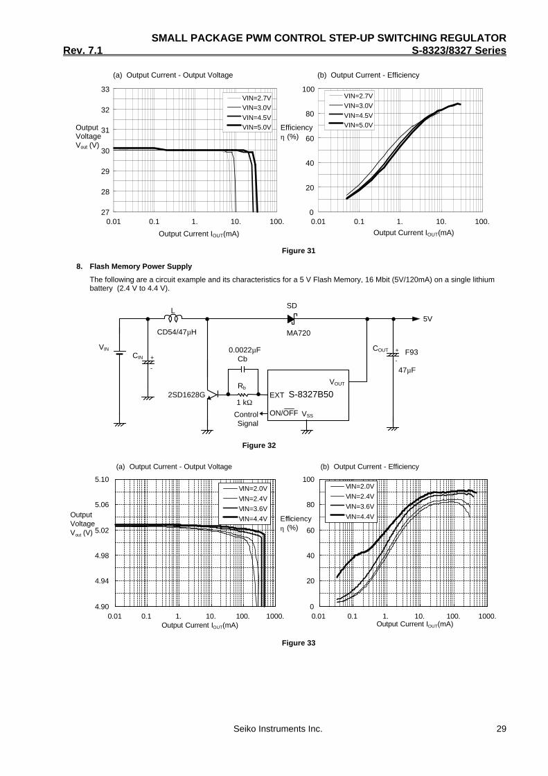
8. Flash Memory Power Supply
The following are a circuit example and its characteristics for a 5 V Flash Memory, 16 Mbit (5V/120mA) on a single lithiumbattery (2.4 V to 4.4 V).
4.90
4.94
4.98
5.02
5.06
5.10
0.01 0.1 1. 10. 100. 1000.
VIN=2.0V
VIN=2.4V
VIN=3.6V
VIN=4.4V
0
20
40
60
80
100
0.01 0.1 1. 10. 100. 1000.
VIN=2.0V
VIN=2.4V
VIN=3.6V
VIN=4.4V
(a) Output Current - Output Voltage (b) Output Current - Efficiency
Output Current IOUT(mA)
OutputVoltageVout (V)
Efficiencyη (%)
Output Current IOUT(mA)
Figure 33
S-8327B50
-
+ -
+
VOUT
47µF
EXT
CIN
VIN
5V
F93COUT
CD54/47µH
1 kΩ
0.0022µF
Rb
ON/OFFControlSignal
VSS
MA720
SDL
2SD1628G
Cb
Figure 32

SMALL PACKAGE PWM CONTROL STEP-UP SWITCHING REGULATORS-8323/8327 Series Rev. 7.1
30 Seiko Instruments Inc.
9. Power Supply for CCD
The follows are a circuit example and its characteristics for CCD power supply (+15, -5.5V/10mA) powered by 4 alkaline-manganese batteries (3.6-6.0V), used for digital still cameras and others.
S-8327J50
Vss-
+ -
+
-
+VIN
Co1
Co2
/F9310u
10u
CEE93
10 30
11
MA720
MA720
100u
100uH
VDD VOUT
EXT
CIN
NDS335N
k
k
RA
270
RB
140
Cc
30p
/F93
VOUT+
+15V
VOUT -
-5.5VTR1
Figure 34
(a) Output Current - Output Voltage (positive output) (b) Output Current - Output Voltage (negative output)
14
14.4
14.8
15.2
15.6
16
0.1 1 10 100
VIN=3.0 V
VIN=3.6 V
VIN=6.0 V
OutputVoltageVOUT
(V)
Output Current IOUT (mA)
-6.5
-6.1
-5.7
-5.3
-4.9
-4.50.1 1 10 100
VIN=3.0 V
VIN=3.6 V
VIN=6.0 V
OutputVoltageVOUT
(V)
Output Current IOUT (mA)
(c) Output Current - Efficiency
0
20
40
60
80
100
0.1 1 10 100
Output Current IOUT (mA)
Efficiencyη (%)
VIN=3.0VVIN=3.6V
VIN=6.0V
Figure 35

SMALL PACKAGE PWM CONTROL STEP-UP SWITCHING REGULATORRev. 7.1 S-8323/8327 Series
Seiko Instruments Inc. 31
n n Temperature Characteristics
VST1 - Ta VST2 - Ta
ISS1 - Ta ISS2 - Ta
ISSS - Ta ISW - Ta
ISWQ - Ta fosc - Ta
20 8060400-20-40 1000.0
VOUT=3.0V, fosc=50kHz type1.2
1.0
0.8
0.6
0.4
0.2
VST1
(V)
Ta (°C)
S-8323
20 8060400-20-40 1000.0
VOUT=3.0V, fosc=50kHz type
0.2
0.4
0.6
0.8
1.0
VST2
(V)
Ta (°C)
S-8323
20 8060400-20-40 1000
VOUT=3.0V, fosc=50kHz type
10
20
30
40
50
Ta (°C)
ISS1
(µA)
S-8323
20 8060400-20-40 1000
VOUT=3.0V, fosc=50kHz type
1
2
3
4
5
Ta (°C)
ISS2
(µA)
S-8323
S-8323
20 8060400-20-40 1000.0
VOUT=3.0V, fosc=50kHz type
0.2
0.4
0.6
0.8
1.0
Ta (°C)
ISSS
(µA)
S-8323
20 8060400-20-40 1000
VOUT=3.0V, fosc=50kHz type200
175
150
125
100
75
50
25
Ta (°C)
ISW
(mA)
20 8060400-20-40 1000.0
VOUT=3.0V, fosc=50kHz type
0.2
0.4
0.6
0.8
1.0
ISWQ
(µA)
S-8323
Ta (°C) 20 8060400-20-40 10030
VOUT=3.0V, fosc=50kHz type70
65
60
55
50
45
40
35
fosc
(kHz)
S-8323
Ta (°C)

SMALL PACKAGE PWM CONTROL STEP-UP SWITCHING REGULATORS-8323/8327 Series Rev. 7.1
32 Seiko Instruments Inc.
MaxDuty - Ta
VSH - Ta VSL1 - Ta
VSL2 - Ta TSS - Ta
IEXTH - Ta IEXTL - Ta
20 8060400-20-40 10050
S-8323 VOUT=3.0V, fosc=50kHz type
60
70
80
90
100
MaxDuty
(%)
Ta (°C)
20 8060400-20-40 1000.0
S-8323 VOUT=3.0V, fosc=50kHz type
0.2
0.4
0.6
0.8
1.0
VSH
(V)
Ta (°C)
20 8060400-20-40 1000.0
S-8323 VOUT=3.0V, fosc=50kHz type
0.2
0.4
0.6
0.8
1.0
VSL1
(V)
Ta (°C)
20 8060400-20-40 1000.0
S-8323 VOUT=3.0V, fosc=50kHz type
0.2
0.4
0.6
0.8
1.0
Ta (°C)
VSL2
(V)
20 8060400-20-40 100
S-8323 VOUT=3.0V, fosc=50kHz type14.0
12.0
10.0
8.0
6.0
4.0
2.0
0.0
Ta (°C)
TSS
(mS)
20 8060400-20-40 100-0
S-8327 VOUT=3.0V, fosc=100kHz type-16
-14
-12
-10
-8
-6
-4
-2
IEXTH
(mA)
Ta (°C)
S-8327 VOUT=3.0V, fosc=100kHz type
20 8060400-20-40 1000
16
14
12
10
8
6
4
2
IEXTL
(mA)
Ta (°C)

SMALL PACKAGE PWM CONTROL STEP-UP SWITCHING REGULATORRev. 7.1 S-8323/8327 Series
Seiko Instruments Inc. 33
VST1 - Ta VST2 - TaS-8323 VOUT=3.3V, fosc=250kHz type S-8323 VOUT=3.3V, fosc=250kHz type
0.0
0.2
0.4
0.6
0.8
1.0
1.2
-40 -20 0 20 40 60 80 100Ta(°C)
VST
(V)
0
0.2
0.4
0.6
0.8
1
-40 -20 0 20 40 60 80 100Ta(°C)
VST2
(V)
ISS1 - Ta ISs2 - TaS-8323 VOUT=3.3V, fosc=250kHz type S-8323 VOUT=3.3V, fosc=250kHz type
0
20
40
60
80
100
ISS1
(µA)
-40 -20 0 20 40 60 80 100Ta(°C)
0
2
4
6
8
10
12
ISS2
(µA)
-40 -20 0 20 40 60 80 100Ta(°C)
fOSC - Ta MaxDuty - TaS-8323 VOUT=3.3V, fosc=250kHz type S-8323 VOUT=3.3V, fosc=250kHz type
220
230
240
250
260
270
280
-40 -20 0 20 40 60 80 100
Ta(°C)
fosc(kHz)
50
60
70
80
90
100
-40 -20 0 20 40 60 80 100
MaxDuty(%)
Ta(°C)

SMALL PACKAGE PWM CONTROL STEP-UP SWITCHING REGULATORS-8323/8327 Series Rev. 7.1
34 Seiko Instruments Inc.
n n Voltage Characteristics
ISS1, 2 - VDD ISW - VDD
fosc - VDD
ISS1, 2-VDD fosc - VDD
S-8323J50 Ta=25°C, VOUT=5.0V, fosc=50kHz type S-8323J50 Ta=25°C, VOUT=5.0V, fosc=50kHz type
0
100
200
300
0 2 4 6 8 10VDD(V)
ISS1
ISS2
(µA)
100
200
300
0 1 2 3 4 5VDD(V)
fosc(kHz)
2 8640 100
S-8323 Ta=25°C, VOUT=5.0V, fosc=50kHz type
10
20
30
40
50
VDD (V)
ISS1
ISS2
(µA)
S-8323
1 4320 50
Ta=25°C, VOUT=5.0V, fosc=50kHz type
50
100
150
200
250
VDD (V)
ISW
(mA)
1 4320 530
S-8323 Ta=25°C, VOUT=5.0V, fosc=50kHz type
40
50
60
70
fosc
(kHz)
VDD (V)

SMALL PACKAGE PWM CONTROL STEP-UP SWITCHING REGULATORRev. 7.1 S-8323/8327 Series
Seiko Instruments Inc. 35
n n Ripple Characteristics
S-8323A301. Light Load (IOUT=200µA) VIN=1.8V
t (10 µsec/div)
OutputVoltage
(10mV/div)
0V
3V
CONTVoltage(1V/div)
2. Medium Load (IOUT=10mA) VIN=1.8V
t (10 µsec/div)
OutputVoltage
(10mV/div)
0V
3V
CONTVoltage(1V/div)
3. Heavy Load (IOUT=60mA) VIN=1.8V
t (10 µsec/div)
OutputVoltage
(10mV/div)
0V
3V
CONTVoltage(1V/div)
S-8327B301. Light Load (IOUT=200µA) VIN=1.8V
t (5 µsec/div)
OutputVoltage
(10mV/div)
0V
3V
CONTVoltage(1V/div)
2. Medium Load (IOUT=10mA) VIN=1.8V
t (5 µsec/div)
OutputVoltage
(10mV/div)
0V
3V
CONTVoltage(1V/div)
3. Heavy Load (IOUT=200mA) VIN=1.8V
t (5 µsec/div)
OutputVoltage
(20mV/div)
0V
3V
CONTVoltage(1V/div)

SMALL PACKAGE PWM CONTROL STEP-UP SWITCHING REGULATORS-8323/8327 Series Rev. 7.1
36 Seiko Instruments Inc.
n n Transient Responses
1. Powering ON due to VIN (VIN: 0V → 1.8 V)
S-8323A30 (Light Load:IOUT=1mA)
t (1msec/div)
2V
Input Vol.(1V/div)
Output V.(1V/div)
0V
3V
0V
S-8323A30 (Heavy Load:IOUT=60mA)
t (1msec/div)
2V
Input Vol.(1V/div)
Output V.(1V/div)
0V
3V
0V
S-8327B30 (Light Load:IOUT=1mA)
t (1msec/div)
2V
Input Vol.(1V/div)
Output V.(1V/div)
0V
3V
0V
S-8327B30 (Heavy Load:IOUT=200mA)
t (1msec/div)
2V
Input Vol.(1V/div)
Output V.(1V/div)
0V
3V
0V
2. Powering ON due to Shutdown pin (Von/off: 0V → 3.0 V)
S-8323A30 (Light Load:IOUT=1mA)
t (1msec/div)
3V
Input Vol.(1V/div)
Output V.(1V/div)
0V
3V
0V
VIN=1.8V S-8323A30 (Heavy Load:IOUT=60mA)
t (1msec/div)
3V
Input Vol.(1V/div)
Output V.(1V/div)
0V
3V
0V
VIN=1.8V
S-8327B30 (Light Load:IOUT=1mA)
t (1msec/div)
3V
Input Vol.(1V/div)
Output V.(1V/div)
0V
3V
0V
VIN=1.8V S-8327B30 (Heavy Load:IOUT=200mA)
t (1msec/div)
3V
Input Vol.(1V/div)
Output V.(1V/div)
0V
3V
0V
VIN=1.8V

SMALL PACKAGE PWM CONTROL STEP-UP SWITCHING REGULATORRev. 7.1 S-8323/8327 Series
Seiko Instruments Inc. 37
3. Load Fluctuations
S-8323A30 (IOUT:100µA→50mA) VIN=1.8V
t (100µsec/div)
3V
Output Vol.(50mV/div)
100µA
50mA
Load Current
S-8323A30 (IOUT:50mA→100µA) VIN=1.8V
t (5msec/dvi)
3V
Output Vol.(50mV/div)
100µA
50mA
Load Current
S-8327B30 (IOUT:100µA→100mA) VIN=1.8V
t (100µsec/div)
3V
Output Vol.(50mV/div)
100µA
100mA
Load Current
S-8327B30 (IOUT:100mA→100µA) VIN=1.8V
t (5msec/dvi)
3V
Output Vol.(50mV/div)
100µA
100mA
Load Current
There is no significant difference in load/power-voltage fluctuations between A, B, and H types.
4. Power Voltage Fluctuations
S8323A30 (VIN:1.8V→2.4V) IOUT=50mA
t (100µsec/div)
3V
Output Vol.(25mV/div)
Load Current(0.2V/div)
1.8V
2.4V
S8323A30 (VIN:2.4V→1.8V) IOUT=50mA
t (100µsec/div)
3V
Output Vol.(25mV/div)
Load Current(0.2V/div)
1.8V
2.4V
S8327B30 (VIN:1.8V→2.4V) IOUT=100mA
t (100µsec/div)
3V
Output Vol.(25mV/div)
Load Current(0.2V/div)
1.8V
2.4V
S8327B30 (VIN:2.4V→1.8V) IOUT=100mA
t (100µsec/div)
3V
Output Vol.(25mV/div)
Load Current(0.2V/div)
1.8V
2.4V
There is no significant difference in load/power-voltage fluctuations between A, B, and H types.

SMALL PACKAGE PWM CONTROL STEP-UP SWITCHING REGULATORS-8323/8327 Series Rev. 7.1
38 Seiko Instruments Inc.
n n Operation Start Voltage and Operation Holding Voltage Characteristics for Output Current
(The characteristics measurement circuits are Standard Circuit(1) for S-8323A/H, Standard Circuit(2) for S-8327B, StandardCircuit(8) for S-8327H. The external parts are subject to the electrical properties of each A/B/H type.)
S-8323A30
0.0
0.2
0.4
0.6
0.8
1.0
0 2 4 6 8 10Output Current IOUT (mA)
InputVoltageVIN (V)
VST1
VHLD
S-8323A50
0.0
0.2
0.4
0.6
0.8
1.0
0 2 4 6 8 10Output Current IOUT (mA)
InputVoltageVIN (V)
VST1
VHLD
S-8327B30
0.0
0.2
0.4
0.6
0.8
1.0
0 2 4 6 8 10Output Current IOUT (mA)
InputVoltageVIN (V)
VST1
VHLD
S-8327B50
0.0
0.2
0.4
0.6
0.8
1.0
0 2 4 6 8 10Output Current IOUT (mA)
InputVoltageVIN (V)
VST1
VHLD
0.0
0.2
0.4
0.6
0.8
1.0
1.2
1.4
0 2 4 6 8 10
S-8323H33
Output Current IOUT (mA)
InputVoltageVIN (V)
VST1
VHLD
0.0
0.2
0.4
0.6
0.8
1.0
1.2
1.4
0 2 4 6 8 10
S-8323H50
Output Current IOUT (mA)
InputVoltageVIN (V)
VST1
VHLD
0.0
0.2
0.4
0.6
0.8
1.0
1.2
1.4
0 2 4 6 8 10
S-8327H33
Output Current IOUT (mA)
InputVoltageVIN (V)
VST1
VHLD0.0
0.2
0.4
0.6
0.8
1.0
1.2
1.4
0 2 4 6 8 10
S-8327H50
Output Current IOUT (mA)
InputVoltageVIN (V)
VST1
VHLD

SMALL PACKAGE PWM CONTROL STEP-UP SWITCHING REGULATORRev. 7.1 S-8323/8327 Series
Seiko Instruments Inc. 39
n n Input Voltage Characteristics for Input Current
(The characteristics measurement circuits are Standard Circuit(1) for S-8323A/H, Standard Circuit(2) for S-8327B, StandardCircuit(8) for S-8327H. The external parts are compatible with the specified conditions of electrical characteristics of Types A, Band H, respectively. The input current adopted for the measuring condition is the consumption current from VIN under no load.)
0
100
200
300
400
0 1 2 3 4 5
VOUT=2VVOUT=3VVOUT=5V
S-8323A
Input Voltage VIN (V)
InputCurrentIIN (µA)
0
10
20
30
40
50
0 1 2 3 4 5
VOUT=3V,Rb=300Ω
VOUT=3V,Rb=1kΩ
VOUT=5V,Rb=300Ω
VOUT=5V,Rb=1kΩ
S-8327B
Input Voltage VIN (V)
InputCurrentIIN (mA)
0
100
200
300
400
500
600
700
1 2 3 4 5
VOUT=2.5VVOUT=3.3VVOUT=5.0V
S-8323H
Input Voltage VIN (V)
InputCurrentIIN (µA)
0
1
2
3
4
5
6
7
8
1 2 3 4 5
VOUT=3.3VVOUT=5.0V
S-8327H
Input Voltage VIN (V)
InputCurrentIIN (mA)

SMALL PACKAGE PWM CONTROL STEP-UP SWITCHING REGULATORS-8323/8327 Series Rev. 7.1
40 Seiko Instruments Inc.
n n Reference Data
Use reference data to choose the external parts.
Reference data give yor the procedure to choose the recommended external parts for various applications and its characteristicsdata.
1. Classification of Products and Inductors by Usage
The products are classified in general into built-in/external switching transistor(S-8323/7) types and low/high switchingfrequency(A,B/H) types.
Compared with built-in switching transistors, external switching transistors can yield larger output current but their efficiencydecreases in a small output current range(especially less than 1mA).
Compared with low frequency models, the high frequency models can yield smaller external parts, in particular inductors, andsmaller output ripple voltage. However, they need more than two alkaline-manganese battery cells(operation voltageincreases from 0.9V to 1.4V).
And the efficiency decreases in a small output current range(especially less than 1mA).
The figures below summarize above features. Please refer to those figures when choosing your models.
Output Current
S-8323H Type
(built-in switching transistor)
2V
3V
5V
CDH113
D62F
D62F
S-8327H Type
(external switching transistor)
10mA 100mA 1A
OutputVoltage
CDRH4D18
Figure 36 Classification of Inductors by Output Current
S-8327B TypeS-8323A Type
(built-in switching transistor)
LQH3C2V
3V
5V
LQH4NCD54
CD105
CD54
(external switching transistor)
10mA 100mA 1A
OutputVoltage
Output Current

SMALL PACKAGE PWM CONTROL STEP-UP SWITCHING REGULATORRev. 7.1 S-8323/8327 Series
Seiko Instruments Inc. 41
2. Procedure to choose the most suitable condition from reference data.
Please refer to the procedures shown below when choosing external parts based on the reference data.
START
Choose the desired output voltage
Choose the condition for desired outputcurrent
Operation efficiency ismore important rather thanstand-by efficiency?
*1
*2
*3
No
Yes
Choose the best condition for operation efficiency.
Stand-by
efficiency is OK?
*4Choose next bestcondition for operationefficiency
Choose the best condition for stand-by efficiency.
Operation efficiency is OK?
*4*4
Choose next bestcondition for operationefficiencyNo
*4
*5
Ripple voltage is OK?Increase output
current
Yes
*5
No
END
Yes
*4
*4
*1) Choose desired output voltage from conditions (1) to (29) shown in Table 1 and 2.
When desired output voltage does not exist in Tables, choose the next higher voltage.
For instance, when VOUT=3V for S-8323A, choose from conditions (3) to (6).
*2) Choose all conditions from conditions choosed above for output current needed for input voltage (min) of the
operational condition from “Reference data 1 (a) output voltage characteristics for output current”.
For instance, when 10mA output current is needed at VIN=0.9V, choose from conditions (4) to (6).
*3) Stand-by efficiency means the efficiency when the output current is small (approx. 100µA), operation efficiency
means the efficiency when the output current is large (several mA).
For instance, go to “YES” when operation efficiency is more important rather than stand-by efficiency.
*4) Read the efficiency for input voltage and output current in operational condition from “Reference data 1 (b)
efficiency characteristics for output current”.
For instance, when VIN =0.9V at IOUT=10mA, the efficiency is max. (75%) in condition (6) in (4) to (6).
There is no difference between conditions (4) to (6) when the output current is 100µA at stand-by condition.
Therefore, choose condition (6).
*5) Read the ripple voltage under the operational condition selected above from “Reference data 2 ripple voltage
characteristics for output current”.
For instance, when condition (6) is selected above, the ripple voltage is 12mV at VIN=0.9V and IOUT=10mA.
No
Yes
SMALL PACKAGE PWM CONTROL STEP-UP SWITCHING REGULATORS-8323/8327 Series Rev. 7.1
42 Seiko Instruments Inc.
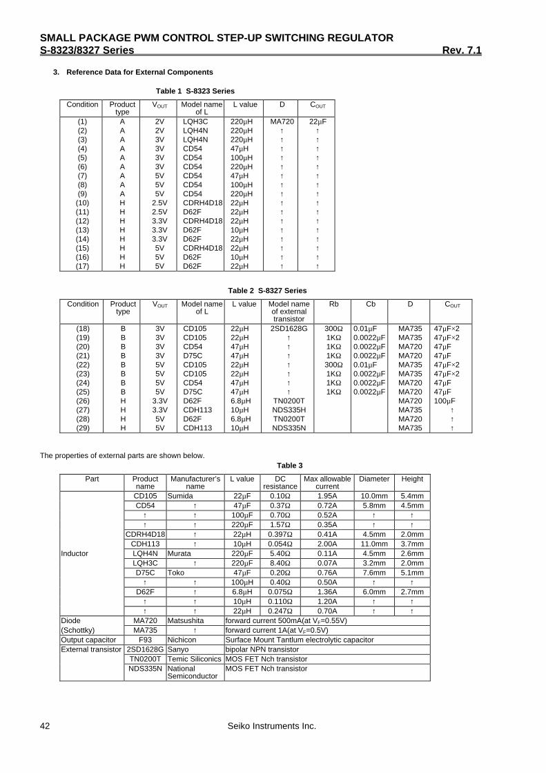
3. Reference Data for External Components
Table 1 S-8323 Series
Condition Producttype
VOUT Model nameof L
L value D COUT
(1)(2)(3)(4)(5)(6)(7)(8)(9)
(10)(11)(12)(13)(14)(15)(16)(17)
AAAAAAAAAHHHHHHHH
2V2V3V3V3V3V5V5V5V
2.5V2.5V3.3V3.3V3.3V5V5V5V
LQH3CLQH4NLQH4NCD54CD54CD54CD54CD54CD54CDRH4D18D62FCDRH4D18D62FD62FCDRH4D18D62FD62F
220µH220µH220µH47µH100µH220µH47µH100µH220µH22µH22µH22µH10µH22µH22µH10µH22µH
MA720↑↑↑↑↑↑↑↑↑↑↑↑↑↑↑↑
22µF↑↑↑↑↑↑↑↑↑↑↑↑↑↑↑↑
Table 2 S-8327 Series
Condition Producttype
VOUT Model nameof L
L value Model nameof externaltransistor
Rb Cb D COUT
(18)(19)(20)(21)(22)(23)(24)(25)(26)(27)(28)(29)
BBBBBBBBHHHH
3V3V3V3V5V5V5V5V
3.3V3.3V5V5V
CD105CD105CD54D75CCD105CD105CD54D75CD62FCDH113D62FCDH113
22µH22µH47µH47µH22µH22µH47µH47µH6.8µH10µH6.8µH10µH
2SD1628G↑↑↑↑↑↑↑
TN0200TNDS335HTN0200TNDS335N
300Ω1KΩ1KΩ1KΩ300Ω1KΩ1KΩ1KΩ
0.01µF0.0022µF0.0022µF0.0022µF0.01µF0.0022µF0.0022µF0.0022µF
MA735MA735MA720MA720MA735MA735MA720MA720MA720MA735MA720MA735
47µF×247µF×247µF47µF47µF×247µF×247µF47µF100µF
↑↑↑
The properties of external parts are shown below.Table 3
Part Productname
Manufacturer’sname
L value DCresistance
Max allowablecurrent
Diameter Height
CD105 Sumida 22µF 0.10Ω 1.95A 10.0mm 5.4mmCD54 ↑ 47µF 0.37Ω 0.72A 5.8mm 4.5mm
↑ ↑ 100µF 0.70Ω 0.52A ↑ ↑↑ ↑ 220µF 1.57Ω 0.35A ↑ ↑
CDRH4D18 ↑ 22µH 0.397Ω 0.41A 4.5mm 2.0mmCDH113 ↑ 10µH 0.054Ω 2.00A 11.0mm 3.7mm
Inductor LQH4N Murata 220µF 5.40Ω 0.11A 4.5mm 2.6mmLQH3C ↑ 220µF 8.40Ω 0.07A 3.2mm 2.0mmD75C Toko 47µF 0.20Ω 0.76A 7.6mm 5.1mm
↑ ↑ 100µH 0.40Ω 0.50A ↑ ↑D62F ↑ 6.8µH 0.075Ω 1.36A 6.0mm 2.7mm
↑ ↑ 10µH 0.110Ω 1.20A ↑ ↑↑ ↑ 22µH 0.247Ω 0.70A ↑ ↑
Diode MA720 Matsushita forward current 500mA(at VF=0.55V)(Schottky) MA735 ↑ forward current 1A(at VF=0.5V)Output capacitor F93 Nichicon Surface Mount Tantlum electrolytic capacitorExternal transistor 2SD1628G Sanyo bipolar NPN transistor
TN0200T Temic Siliconics MOS FET Nch transistorNDS335N National
SemiconductorMOS FET Nch transistor

SMALL PACKAGE PWM CONTROL STEP-UP SWITCHING REGULATORRev. 7.1 S-8323/8327 Series
Seiko Instruments Inc. 43
4. Reference Data 1
Output voltage characteristics for output current and (b) efficiency characteristics for output current under conditions (1) to(29) shown in Tables 1 and 2 are shown below.
(1)S-8323A20(LQH3C:220µµH)
1.95
1.97
1.99
2.01
2.03
2.05
0.01 0.1 1. 10. 100.Output Current IOUT (mA)
OutputVoltageVOUT (V)
VIN=0.9VVIN=1.0VVIN=1.2VVIN=1.6V
(a) Output Current - Output Voltage
50
60
70
80
90
100
0.01 0.1 1. 10. 100.
Output Current IOUT (mA)
Efficiencyη (%)
VIN=0.9VVIN=1.0VVIN=1.2VVIN=1.6V
(b) Output Current - Efficiency
(2)S-8323A20(LQH4N:220µµH)
Output Current IOUT (mA)
OutputVoltageVOUT (V)
(a) Output Current - Output Voltage
1.95
1.97
1.99
2.01
2.03
2.05
0.01 0.1 1. 10. 100.
VIN=0.9VVIN=1.0VVIN=1.2VVIN=1.6V
50
60
70
80
90
100
0.01 0.1 1. 10. 100.
Output Current IOUT (mA)
Efficiencyη (%)
VIN=0.9VVIN=1.0VVIN=1.2VVIN=1.6V
(b) Output Current - Efficiency

SMALL PACKAGE PWM CONTROL STEP-UP SWITCHING REGULATORS-8323/8327 Series Rev. 7.1
44 Seiko Instruments Inc.
(3)S-8323A30(LQH4N:220µµH)
2.95
2.97
2.99
3.01
3.03
3.05
0.01 0.1 1. 10. 100. 1000.
VIN=0.9VVIN=1.2VVIN=1.8VVIN=2.4V
Output Current IOUT (mA)
OutputVoltageVOUT
(V)
(a) Output Current - Output Voltage
50
60
70
80
90
100
0.01 0.1 1. 10. 100. 1000.
VIN=0.9VVIN=1.2VVIN=1.8VVIN=2.4V
Output Current IOUT (mA)
Efficiencyη (%)
(b) Output Current - Efficiency
(4)S-8323A30(CD54:47µµH)
2.95
2.97
2.99
3.01
3.03
3.05
0.01 0.1 1. 10. 100. 1000.
VIN=0.9VVIN=1.0VVIN=1.2VVIN=1.6V
Output Current IOUT (mA)
OutputVoltageVOUT
(V)
(a) Output Current - Output Voltage
50
60
70
80
90
100
0.01 0.1 1. 10. 100. 1000.
VIN=0.9VVIN=1.0VVIN=1.2VVIN=1.6V
Output Current IOUT (mA)
Efficiencyη (%)
(b) Output Current - Efficiency
(5)S-8323A30(CD54:100µµH)
2.95
2.97
2.99
3.01
3.03
3.05
0.01 0.1 1. 10. 100. 1000.
VIN=0.9VVIN=1.2VVIN=1.8VVIN=2.4V
Output Current IOUT (mA)
OutputVoltageVOUT
(V)
(a) Output Current - Output Voltage
50
60
70
80
90
100
0.01 0.1 1. 10. 100. 1000.
VIN=0.9VVIN=1.2VVIN=1.8VVIN=2.4V
Output Current IOUT (mA)
Efficiencyη (%)
(b) Output Current - Efficiency
(6)S-8323A30(CD54:220µµH)
2.95
2.97
2.99
3.01
3.03
3.05
0.01 0.1 1. 10. 100. 1000.
VIN=0.9VVIN=1.2VVIN=1.8VVIN=2.4V
Output Current IOUT (mA)
OutputVoltageVOUT
(V)
(a) Output Current - Output Voltage
50
60
70
80
90
100
0.01 0.1 1. 10. 100. 1000.
VIN=0.9VVIN=1.2VVIN=1.8VVIN=2.4V
Output Current IOUT (mA)
Efficiencyη (%)
(b) Output Current - Efficiency

SMALL PACKAGE PWM CONTROL STEP-UP SWITCHING REGULATORRev. 7.1 S-8323/8327 Series
Seiko Instruments Inc. 45
(7)S-8323A50(CD54:47µµH)
4.90
4.94
4.98
5.02
5.06
5.10
0.01 0.1 1. 10. 100. 1000.
VIN=0.9VVIN=1.8VVIN=3.0VVIN=4.0V
Output Current IOUT (mA)
OutputVoltageVOUT
(V)
(a) Output Current - Output Voltage
50
60
70
80
90
100
0.01 0.1 1. 10. 100. 1000.Output Current IOUT (mA)
Efficiencyη (%)
(b) Output Current - Efficiency
VIN=0.9VVIN=1.8VVIN=3.0VVIN=4.0V
(8)S-8323A50(CD54:100µµH)
4.90
4.94
4.98
5.02
5.06
5.10
0.01 0.1 1. 10. 100. 1000.
VIN=0.9VVIN=1.8VVIN=3.0VVIN=4.0V
Output Current IOUT (mA)
OutputVoltageVOUT
(V)
(a) Output Current - Output Voltage
50
60
70
80
90
100
0.01 0.1 1. 10. 100. 1000.Output Current IOUT (mA)
Efficiencyη (%)
(b) Output Current - Efficiency
VIN=0.9VVIN=1.8VVIN=3.0VVIN=4.0V
(9)S-8323A50(CD54:220µµH)
4.90
4.94
4.98
5.02
5.06
5.10
0.01 0.1 1. 10. 100. 1000.
VIN=0.9VVIN=1.8VVIN=3.0VVIN=4.0V
Output Current IOUT (mA)
OutputVoltageVOUT
(V)
(a) Output Current - Output Voltage
50
60
70
80
90
100
0.01 0.1 1. 10. 100. 1000.Output Current IOUT (mA)
Efficiencyη (%)
(b) Output Current - Efficiency
VIN=0.9VVIN=1.8VVIN=3.0VVIN=4.0V

SMALL PACKAGE PWM CONTROL STEP-UP SWITCHING REGULATORS-8323/8327 Series Rev. 7.1
46 Seiko Instruments Inc.
(10)S-8323H25(CDRH4D18:22µµH)
2.45
2.47
2.49
2.51
2.53
2.55
0.01 0.1 1 10 100 1000
0
20
40
60
80
100
0.01 0.1 1 10 100 1000
Output Current IOUT (mA)
Efficiencyη (%)
(b) Output Current - Efficiency
VIN=1.5V
(11)S-8323H25(D62F:22µµH)
2.45
2.47
2.49
2.51
2.53
2.55
0.01 0.1 1 10 100 10000
20
40
60
80
100
0.01 0.1 1 10 100 1000
Output Current IOUT (mA)
Efficiencyη (%)
(b) Output Current - Efficiency
VIN=1.5V
(12)S-8323H33(CDRH4D18:22µµH )
3.25
3.27
3.29
3.31
3.33
3.35
0.01 0.1 1 10 100 1000 0
20
40
60
80
100
0.01 0.1 1 10 100 1000
(13)S-8323H33(D62F:10µµH)
3.25
3.27
3.29
3.31
3.33
3.35
0.01 0.1 1 10 100 1000 0
20
40
60
80
100
0.01 0.1 1 10 100 1000
VIN=1.5VVIN=1.8VVIN=3.0V
Output Current IOUT (mA)
Efficiencyη (%)
(b) Output Current - Efficiency
VIN=1.5V
Output Current IOUT (mA)
OutputVoltageVOUT
(V)
(a) Output Current - Output Voltage
VIN=1.5V
Output Current IOUT (mA)
OutputVoltageVOUT
(V)
(a) Output Current - Output Voltage
VIN=1.5VVIN=1.8VVIN=3.0V
Output Current IOUT (mA)
OutputVoltageVOUT
(V)
(a) Output Current - Output Voltage
VIN=1.5VVIN=1.8VVIN=3.0V
Output Current IOUT (mA)
OutputVoltageVOUT
(V)
(a) Output Current - Output Voltage
VIN=1.5VVIN=1.8VVIN=3.0V
Output Current IOUT (mA)
Efficiencyη (%)
(b) Output Current - Efficiency

SMALL PACKAGE PWM CONTROL STEP-UP SWITCHING REGULATORRev. 7.1 S-8323/8327 Series
Seiko Instruments Inc. 47
(14)S-8323H33(D62F:22µµH)
3.25
3.27
3.29
3.31
3.33
3.35
0.01 0.1 1 10 100 1000 0
20
40
60
80
100
0.01 0.1 1 10 100 1000
VIN=1.5VVIN=1.8VVIN=3.0V
Output Current IOUT (mA)
Efficiencyη (%)
(b) Output Current - Efficiency
(15)S-8323H50(CDRH 4D18:22µµH)
4.9
4.94
4.98
5.02
5.06
5.1
0.01 0.1 1 10 100 1000
0
20
40
60
80
100
0.01 0.1 1 10 100 1000
(16)S-8323H50(D62F:10µµH)
4.9
4.94
4.98
5.02
5.06
5.1
0.01 0.1 1 10 100 1000 0
20
40
60
80
100
0.01 0.1 1 10 100 1000
(17)S-8323H50(D62F:22µµH )
4.9
4.94
4.98
5.02
5.06
5.1
0.01 0.1 1 10 100 1000
0
20
40
60
80
100
0.01 0.1 1 10 100 1000
VIN=1.5VVIN=1.8VVIN=3.0V
Output Current IOUT (mA)
OutputVoltageVOUT
(V)
(a) Output Current - Output Voltage
VIN=1.8VVIN=3.0VVIN=4.5V
Output Current IOUT (mA)
OutputVoltageVOUT
(V)
(a) Output Current - Output Voltage
VIN=1.8VVIN=3.0VVIN=4.5V
Output Current IOUT (mA)
OutputVoltageVOUT
(V)
(a) Output Current - Output Voltage
VIN=1.8VVIN=3.0VVIN=4.5V
Output Current IOUT (mA)
OutputVoltageVOUT
(V)
(a) Output Current - Output Voltage
Output Current IOUT (mA)
Efficiencyη (%)
(b) Output Current - Efficiency
VIN=1.8VVIN=3.0VVIN=4.5V
VIN=1.8VVIN=3.0VVIN=4.5V
Output Current IOUT (mA)
Efficiencyη (%)
(b) Output Current - Efficiency
VIN=1.8VVIN=3.0VVIN=4.5V
Output Current IOUT (mA)
Efficiencyη (%)
(b) Output Current - Efficiency

SMALL PACKAGE PWM CONTROL STEP-UP SWITCHING REGULATORS-8323/8327 Series Rev. 7.1
48 Seiko Instruments Inc.
(18)S-8327B30(CD105:22µµH,Rb=300ΩΩ,Cb=0.01µµF)
2.95
2.97
2.99
3.01
3.03
3.05
0.01 0.1 1. 10. 100. 1000.
VIN=0.9VVIN=1.2VVIN=1.8VVIN=2.4V
Output Current IOUT (mA)
OutputVoltageVOUT
(V)
(a) Output Current - Output Voltage
0
20
40
60
80
100
0.01 0.1 1. 10. 100. 1000.
VIN=0.9VVIN=1.2VVIN=1.8VVIN=2.4V
Output Current IOUT (mA)
Efficiencyη (%)
(b) Output Current - Efficiency
(19)S-8327B30(CD105:22µµH,Rb=1kΩΩ,Cb=0.0022µµF)
2.95
2.97
2.99
3.01
3.03
3.05
0.01 0.1 1. 10. 100. 1000.
VIN=0.9VVIN=1.2VVIN=1.8VVIN=2.4V
Output Current IOUT (mA)
OutputVoltageVOUT
(V)
(a) Output Current - Output Voltage
0
20
40
60
80
100
0.01 0.1 1. 10. 100. 1000.
VIN=0.9VVIN=1.2VVIN=1.8VVIN=2.4V
Output Current IOUT (mA)
Efficiencyη (%)
(b) Output Current - Efficiency
(20)S-8327B30(CD54:47µµH,Rb=1kΩΩ,Cb=0.0022µµF)
2.95
2.97
2.99
3.01
3.03
3.05
0.01 0.1 1. 10. 100. 1000.
VIN=0.9VVIN=1.2VVIN=1.8VVIN=2.4V
Output Current IOUT (mA)
OutputVoltageVOUT
(V)
(a) Output Current - Output Voltage
0
20
40
60
80
100
0.01 0.1 1. 10. 100. 1000.
VIN=0.9VVIN=1.2VVIN=1.8VVIN=2.4V
Output Current IOUT (mA)
Efficiencyη (%)
(b) Output Current - Efficiency
(21)S-8327B30(D75C:47µµH,Rb=1kΩΩ,Cb=0.0022µµF)
2.95
2.97
2.99
3.01
3.03
3.05
0.01 0.1 1. 10. 100. 1000.
VIN=0.9VVIN=1.2VVIN=1.8VVIN=2.4V
Output Current IOUT (mA)
OutputVoltageVOUT
(V)
(a) Output Current - Output Voltage
0
20
40
60
80
100
0.01 0.1 1. 10. 100. 1000.Output Current IOUT (mA)
Efficiencyη (%)
(b) Output Current - Efficiency
VIN=1.2VVIN=1.8VVIN=2.4V
VIN=0.9V

SMALL PACKAGE PWM CONTROL STEP-UP SWITCHING REGULATORRev. 7.1 S-8323/8327 Series
Seiko Instruments Inc. 49
(22)S-8327B50(CD105:22µµH,Rb=300ΩΩ,Cb=0.01µµF)
4.90
4.94
4.98
5.02
5.06
5.10
0.01 0.1 1. 10. 100. 1000. 10000.
VIN=0.9VVIN=1.8VVIN=3.0VVIN=4.0V
Output Current IOUT (mA)
OutputVoltageVOUT
(V)
(a) Output Current - Output Voltage
0
20
40
60
80
100
0.01 0.1 1. 10. 100. 1000. 10000.
VIN=0.9VVIN=1.8VVIN=3.0VVIN=4.0V
Output Current IOUT (mA)
Efficiencyη (%)
(b) Output Current - Efficiency
(23)S-8327B50(CD105:22µµH,Rb=1kΩΩ,Cb=0.0022µµF)
4.90
4.94
4.98
5.02
5.06
5.10
0.01 0.1 1. 10. 100. 1000. 10000.
VIN=0.9VVIN=1.8VVIN=3.0VVIN=4.0V
Output Current IOUT (mA)
OutputVoltageVOUT
(V)
(a) Output Current - Output Voltage
0
20
40
60
80
100
0.01 0.1 1. 10. 100. 1000. 10000.
VIN=0.9VVIN=1.8VVIN=3.0VVIN=4.0V
Output Current IOUT (mA)
Efficiencyη (%)
(b) Output Current - Efficiency
(24)S-8327B50(CD54:47µµH,Rb=1kΩΩ,Cb=0.0022µµF)
4.90
4.94
4.98
5.02
5.06
5.10
0.01 0.1 1. 10. 100. 1000. 10000.
VIN=0.9VVIN=1.8VVIN=3.0VVIN=4.0V
Output Current IOUT (mA)
OutputVoltageVOUT
(V)
(a) Output Current - Output Voltage
0
20
40
60
80
100
0.01 0.1 1. 10. 100. 1000. 10000.
VIN=0.9VVIN=1.8VVIN=3.0VVIN=4.0V
Output Current IOUT (mA)
Efficiencyη (%)
(b) Output Current - Efficiency
(25)S-8327B50(D75C:47µµH,Rb=1kΩΩ,Cb=0.0022µµF)
4.90
4.94
4.98
5.02
5.06
5.10
0.01 0.1 1. 10. 100. 1000. 10000.
VIN=0.9VVIN=1.8VVIN=3.0VVIN=4.0V
Output Current IOUT (mA)
OutputVoltageVOUT
(V)
(a) Output Current - Output Voltage
0
20
40
60
80
100
0.01 0.1 1. 10. 100. 1000. 10000.
VIN=0.9VVIN=1.8VVIN=3.0VVIN=4.0V
Output Current IOUT (mA)
Efficiencyη (%)
(b) Output Current - Efficiency

SMALL PACKAGE PWM CONTROL STEP-UP SWITCHING REGULATORS-8323/8327 Series Rev. 7.1
50 Seiko Instruments Inc.
(26)S-8327H33(D62F:6.8µµH)
3.25
3.27
3.29
3.31
3.33
3.35
0.01 0.1 1 10 100 1000
0
20
40
60
80
100
0.01 0.1 1 10 100 1000
Output Current IOUT (mA)
Efficiencyη (%)
(b) Output Current - Efficiency
VIN=1.5VVIN=1.8VVIN=3.0V
(27)S-8327H33(CDH113:10µµH )
3.25
3.27
3.29
3.31
3.33
3.35
0.01 0.1 1 10 100 10000
20
40
60
80
100
0.01 0.1 1 10 100 1000
(28)S-8327H50(D62F:6.8µµH )
4.9
4.94
4.98
5.02
5.06
5.1
0.01 0.1 1 10 100 10000
20
40
60
80
100
0.01 0.1 1 10 100 1000
(29)S-8327H50(CDH113:10µµH)
4.9
4.94
4.98
5.02
5.06
5.1
0.01 0.1 1 10 100 10000
20
40
60
80
100
0.01 0.1 1 10 100 1000
Output Current IOUT (mA)
Efficiencyη (%)
(b) Output Current - Efficiency
VIN=4.5V
VIN=1.8VVIN=3.0V
VIN=1.5VVIN=1.8VVIN=3.0V
Output Current IOUT (mA)
OutputVoltageVOUT
(V)
(a) Output Current - Output Voltage
VIN=1.5VVIN=1.8VVIN=3.0V
Output Current IOUT (mA)
OutputVoltageVOUT
(V)
(a) Output Current - Output Voltage
VIN=4.5V
VIN=1.8VVIN=3.0V
Output Current IOUT (mA)
OutputVoltageVOUT
(V)
(a) Output Current - Output Voltage
VIN=4.5V
VIN=1.8VVIN=3.0V
Output Current IOUT (mA)
OutputVoltageVOUT
(V)
(a) Output Current - Output Voltage
Output Current IOUT (mA)
Efficiencyη (%)
(b) Output Current - Efficiency
VIN=1.5VVIN=1.8VVIN=3.0V
Output Current IOUT (mA)
Efficiencyη (%)
(b) Output Current - Efficiency
VIN=4.5V
VIN=1.8VVIN=3.0V

SMALL PACKAGE PWM CONTROL STEP-UP SWITCHING REGULATORRev. 7.1 S-8323/8327 Series
Seiko Instruments Inc. 51
5. Reference Data 2
The ripple voltage characteristics data is shown below:
(1)S-8323A20 (2)S-8323A20 (LQH3C:220µµH,COUT:22µµF ) (LQH4N:220µµH,COUT:22µµF ) Similar to (2)
0
20
40
60
80
100
0.1 1. 10. 100. 1000.Output Current IOUT (mA)
RippleVoltageVr(mV)
VIN=0.9V
VIN=1.2V
VIN=1.6V
(3)S-8323A30 (LQH4N:220µµH,COUT:22µµF )
Similar to (6)
(4)S-8323A30 (7)S-8323A50 (CD54:47µµH,COUT:22µµF ) (CD54:47µµH,COUT:22µµF )
VIN=0.9V
VIN=1.8V
VIN=2.4V
0
20
40
60
80
100
120
VIN=0.9V
VIN=3.0V
VIN=4.0V
0.1 1. 10. 100. 1000.Output Current IOUT (mA)
RippleVoltageVr(mV)
RippleVoltageVr(mV)
0
20
40
60
80
100
0.1 1. 10. 100. 1000.Output Current IOUT (mA)
(5)S-8323A30 (8)S-8323A50 (CD54:100µµH,COUT:22µµF ) (CD54:100µµH,COUT:22µµF )
0
20
40
60
80
100
VIN=0.9V
VIN=1.8V
VIN=2.4V
VIN=0.9V
VIN=3.0V
VIN=4.0V
0.1 1. 10. 100. 1000.Output Current IOUT (mA)
RippleVoltageVr(mV)
RippleVoltageVr(mV)
0.1 1. 10. 100. 1000.Output Current IOUT (mA)
0
20
40
60
80
100
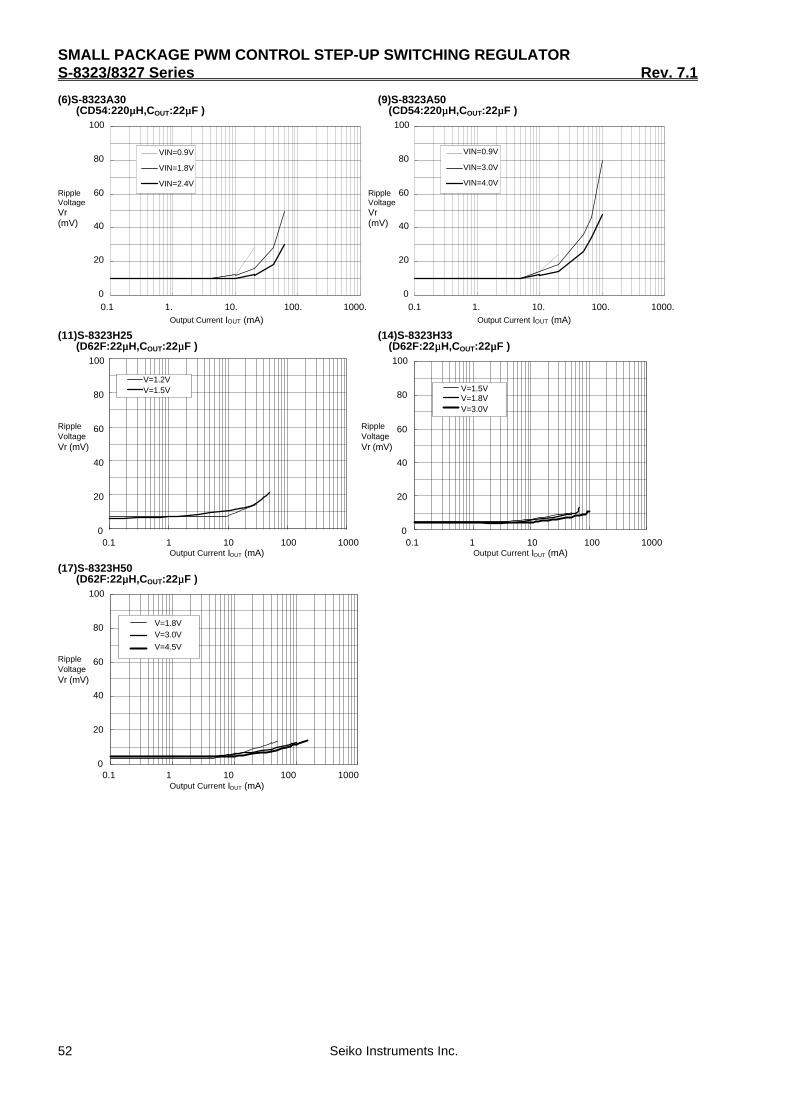
SMALL PACKAGE PWM CONTROL STEP-UP SWITCHING REGULATORS-8323/8327 Series Rev. 7.1
52 Seiko Instruments Inc.
(6)S-8323A30 (9)S-8323A50 (CD54:220µµH,COUT:22µµF ) (CD54:220µµH,COUT:22µµF )
0
20
40
60
80
100
VIN=0.9V
VIN=1.8V
VIN=2.4V
VIN=0.9V
VIN=3.0V
VIN=4.0V
0.1 1. 10. 100. 1000.Output Current IOUT (mA)
RippleVoltageVr(mV)
RippleVoltageVr(mV)
0.1 1. 10. 100. 1000.Output Current IOUT (mA)
0
20
40
60
80
100
(11)S-8323H25 (14)S-8323H33 (D62F:22µµH,COUT:22µµF ) (D62F:22µµH,COUT:22µµF )
0
20
40
60
80
100
0.1 1 10 100 1000
V=1.2VV=1.5V
Output Current IOUT (mA)
RippleVoltageVr (mV)
0
20
40
60
80
100
0.1 1 10 100 1000
V=3.0VV=1.8VV=1.5V
Output Current IOUT (mA)
RippleVoltageVr (mV)
(17)S-8323H50 (D62F:22µµH,COUT:22µµF )
0
20
40
60
80
100
0.1 1 10 100 1000
V=4.5V
V=3.0VV=1.8V
Output Current IOUT (mA)
RippleVoltageVr (mV)

SMALL PACKAGE PWM CONTROL STEP-UP SWITCHING REGULATORRev. 7.1 S-8323/8327 Series
Seiko Instruments Inc. 53
(18)(11)S-8327B30 (22)(23)S-8327B50 (CD105:22µµH,COUT:47µµF××2 ) (CD105:22µµH,COUT:47µµF××2 )
VIN=0.9V
VIN=3.0V
VIN=4.0V
0
20
40
60
80
100
0.1 1 10 100 1000Output Current IOUT (mA)
RippleVoltageVr(mV)
VIN=0.9V
VIN=1.8V
VIN=2.4V
0
20
40
60
80
100
0.1 1 10 100 1000Output Current IOUT (mA)
RippleVoltageVr(mV)
(20)S-8327B30 (24)S-8327B50 (CD54:47µµH,COUT:47µµF) (CD54:47µµH,COUT:47µµF )
VIN=0.9V
VIN=3.0V
VIN=4.0V
0
20
40
60
80
100
0.1 1 10 100 1000Output Current IOUT (mA)
RippleVoltageVr(mV)
VIN=0.9V
VIN=1.8V
VIN=2.4V
0
20
40
60
80
100
0.1 1 10 100 1000Output Current IOUT (mA)
RippleVoltageVr(mV)
(21)S-8327B30 (25)S-8327B50 (D75C:47µµH,COUT:47µµF) (D75C:47µµH,COUT:47µµF) Similar to (20) Similar to (24)
(27)S-8327H33 (29)S-8327H50 (CDH113:10µµH,COUT:100µµF) (CDH113:10µµH,COUT:100µµF)
V=3.0V
V=1.8VV=1.5V
Output Current IOUT (mA)
RippleVoltageVr (mV)
0
20
40
60
80
100
0.1 1 10 100 1000
V=4.5V
V=3.0V
V=1.8V
Output Current IOUT (mA)
RippleVoltageVr (mV)
0
20
40
60
80
100
0.1 1 10 100 1000

T2
1.6±0.1
0.25±0.05
4.0±0.12.0±0.1
4.0±0.1
1.5+0.1 -0.05
1.1±0.1
2.85±0.2
SOT-23-3MP003-A 990531
2.9 0.2
0.95 0.1
1.9 0.2
+0.1 -0.050.16
0.4±0.1
0.25
+0.2 -0.62.8
0 0.1
1
2 3
21±0.5
2±0.2
(60°)(60°)
φ13±0.2
12.5max.
9.0±0.3
1.5
1.3max.1.1±0.1
Winding core
Unit:mmDimensions
Taping Specifications Reel Specifications1 reel holds 3000 ICs.
Feed direction

3.25±0.15
ø1.5 +0.1 -0
ø1.0 +0.1 -0 4.0±0.1
2.0±0.050.27±0.05
1.4±0.2
Feed direction
SOT-23-5 MP005-A 991105
0.95 0.1
2.9±0.2
+0.1 -0.060.16
1.9±0.2
0.4±0.1
1 2 3
45
21±0.5
2±0.2
(60°)(60°)
φ13±0.2
12.5max.
9.0±0.3
+0.2 -0.32.81.6
1.1±0.1
0.45
1.3max
3 max.
3 max.
4.0±0.1 (10 pitches 40.0±0.2)
Taping Specifications Reel Specifications
Dimensions Unit mm
3000 pcs./reel

2.0±0.1
0.3±0.05
4.0±0.1 10 pitches 40.0±0.2
8.0±0.1
ø1.5+0.1 -0
2.0±0.05
ø1.5+0.1 -0
4.75±0.1
13.0±0.3
16.5max
(60°)(60°)
SOT-89-3UP003-A 990531
1.5±0.14.5±0.1
1.6±0.2
1.5±0.1 1.5±0.1
0.45±0.1
0.4±0.10.4±0.1
45
31 2
5 ° max.
Winding core
Unit:mmDimensions
Taping Specifications Reel Specifications1 reel holds 1000 ICs.
Feed direction

1
SOT-23-5
Markings990603
SOT-89-3
1
8323/8324
SOT-23-3

• The information herein is subject to change without notice.
• Seiko Instruments Inc. is not responsible for any problems caused by circuits or other diagrams
described herein whose industrial properties, patents or other rights belong to third parties. The
application circuit examples explain typical applications of the products, and do not guarantee any
mass-production design.
• When the products described herein include Strategic Products (or Service) subject to regulations,
they should not be exported without authorization from the appropriate governmental authorities.
• The products described herein cannot be used as part of any device or equipment which influences
the human body, such as physical exercise equipment, medical equipment, security system, gas
equipment, vehicle or airplane, without prior written permission of Seiko Instruments Inc.