Embed Size (px)
Citation preview
bus
SM8000 SERIES
OPTICAL SWITCH
USER’S MANUAL
P/N: 82-0052-000 Released February 12, 2010
VXI Technology, Inc.
2031 Main Street Irvine, CA 92614-6509
(949) 955-1894

VXI Technology, Inc.
2
VXI Technology, Inc.
SM8000 Series Preface 3
TABLE OF CONTENTS INTRODUCTION
Certification ......................................................................................................................................................6 Warranty ...........................................................................................................................................................6 Limitation of Warranty .....................................................................................................................................6 Restricted Rights Legend ..................................................................................................................................6
DECLARATION OF CONFORMITY..............................................................................................................................7 GENERAL SAFETY INSTRUCTIONS ...........................................................................................................................9
Terms and Symbols...........................................................................................................................................9 Warnings...........................................................................................................................................................9
SUPPORT RESOURCES............................................................................................................................................11 SECTION 1 ...................................................................................................................................................................13
INTRODUCTION .......................................................................................................................................................13 Overview.........................................................................................................................................................13 SM8000 Series - Optical Switch Controller....................................................................................................14 SM8001 / SM8002 - Multi-Channel Switches................................................................................................15 Configurations.................................................................................................................................................15 SM8001 / SM8002 Multi Switch Specifications ............................................................................................17 SM8003 - Prism Switches...............................................................................................................................18 Configurations.................................................................................................................................................18 SM8201 / SM8202 - Optical Attenuators .......................................................................................................20
SECTION 2 ...................................................................................................................................................................21 PREPARATION FOR USE...........................................................................................................................................21
Introduction.....................................................................................................................................................21 Calculating System Power and Cooling Requirements...................................................................................21 Setting the Chassis Backplane Jumpers ..........................................................................................................21 Setting the Logical Address ............................................................................................................................22 Example 1 .......................................................................................................................................................22 Example 2 .......................................................................................................................................................23 Selecting the Extended Memory Space...........................................................................................................23 Optical Connections........................................................................................................................................24 Cleaning Optical Connectors ..........................................................................................................................24 Mating Optical Connectors .............................................................................................................................24
SECTION 3 ...................................................................................................................................................................25 OPERATION.............................................................................................................................................................25
General Description ........................................................................................................................................25 SM8001 / SM8002 - Multi-Channel Switches................................................................................................25 SM8003 - Prism Switches...............................................................................................................................26 SM8201 / SM8202 - Optical Attenuators .......................................................................................................27 Operation.........................................................................................................................................................28 SM8001 / SM8002 - Multi-Channel Switches................................................................................................28
Resetting the Switch ..................................................................................................................................28 Relay Registers - Output Channel Selection..............................................................................................28 1 x N Switch Configuration.......................................................................................................................29 Duplex 1 x N Switch Configuration ..........................................................................................................30 2 x N Blocking Switch Configuration .......................................................................................................31 2 x N Non-Blocking Switch Configuration ...............................................................................................32 Calculating Switching Time ......................................................................................................................33
SM8003 - Prism Switches...............................................................................................................................34 SM8201 / SM8202 - Optical Attenuators .......................................................................................................34
Starting the Device ....................................................................................................................................35
VXI Technology, Inc.
4 SM8000 Series Preface
Control Modes ...........................................................................................................................................35 Uncalibrated Operation - Move-To-Absolute-Step ...................................................................................35 Calibrated Operation..................................................................................................................................35 BUSY Signal .............................................................................................................................................36 ERROR Status ...........................................................................................................................................36 Resetting the Device ..................................................................................................................................36 Commanding the Devices..........................................................................................................................36
SECTION 4 ...................................................................................................................................................................37 PROGRAMMING.......................................................................................................................................................37
Register Access ...............................................................................................................................................37 Addressing ......................................................................................................................................................37 SMIP II Registers - A16 .................................................................................................................................39 Module Registers - SM8000 Series Controller - A24 / A32 - Extended Memory..........................................48
DEVICE MEMORY..................................................................................................................................................54 Module Relay Control Address - SM8000 Series Optical Switch Controller.................................................54 Relay Register Offset ......................................................................................................................................54 Writing to the Relay Registers ........................................................................................................................55
PROGRAMMING EXAMPLES ...................................................................................................................................57 Typical Optical Multi-Switch Control Example .............................................................................................57 Typical Optical Attenuator Control Example .................................................................................................58
COMMAND REGISTER .............................................................................................................................................60 Write Example ................................................................................................................................................60 Read Example .................................................................................................................................................60 Command Set..................................................................................................................................................61 30h ..................................................................................................................................................................62 31h ..................................................................................................................................................................62 32h ..................................................................................................................................................................63 35h ..................................................................................................................................................................63 43h ..................................................................................................................................................................63 6Ch..................................................................................................................................................................64 80h ..................................................................................................................................................................64 81h ..................................................................................................................................................................65 82h ..................................................................................................................................................................65 83h ..................................................................................................................................................................66 89h ..................................................................................................................................................................66 8Ah..................................................................................................................................................................67 8Bh..................................................................................................................................................................67 8Ch..................................................................................................................................................................68 8Dh..................................................................................................................................................................68 8Eh ..................................................................................................................................................................69 90h ..................................................................................................................................................................70 96h ..................................................................................................................................................................71 A2h..................................................................................................................................................................71
INDEX ..........................................................................................................................................................................73

VXI Technology, Inc.
SM8000 Series Preface 5

VXI Technology, Inc.
6 SM8000 Series Preface
CERTIFICATION
VXI Technology, Inc. (VTI) certifies that this product met its published specifications at the time of shipment from the factory. VTI further certifies that its calibration measurements are traceable to the United States National Institute of Standards and Technology (formerly National Bureau of Standards), to the extent allowed by that organization’s calibration facility, and to the calibration facilities of other International Standards Organization members. WARRANTY
The product module referred to herein is warranted against defects in material and workmanship for a period of one year from the receipt date of the product at customer’s facility. The same warranty applies to the optical device options (SM8XXX) for a period of one year. The sole and exclusive remedy for breach of any warranty concerning these goods shall be repair or replacement of defective parts, or a refund of the purchase price, to be determined at the option of VTI. For warranty service or repair, this product must be returned to a VXI Technology authorized service center. The product shall be shipped prepaid to VTI and VTI shall prepay all returns of the product to the buyer. However, the buyer shall pay all shipping charges, duties, and taxes for products returned to VTI from another country. VTI warrants that its software and firmware designated by VTI for use with a product will execute its programming when properly installed on that product. VTI does not however warrant that the operation of the product, or software, or firmware will be uninterrupted or error free. LIMITATION OF WARRANTY
The warranty shall not apply to defects resulting from improper or inadequate maintenance by the buyer, buyer-supplied products or interfacing, unauthorized modification or misuse, operation outside the environmental specifications for the product, or improper site preparation or maintenance. VXI Technology, Inc. shall not be liable for injury to property other than the goods themselves. Other than the limited warranty stated above, VXI Technology, Inc. makes no other warranties, express or implied, with respect to the quality of product beyond the description of the goods on the face of the contract. VTI specifically disclaims the implied warranties of merchantability and fitness for a particular purpose. RESTRICTED RIGHTS LEGEND
Use, duplication, or disclosure by the Government is subject to restrictions as set forth in subdivision (b)(3)(ii) of the Rights in Technical Data and Computer Software clause in DFARS 252.227-7013.
VXI Technology, Inc. 2031 Main Street Irvine, CA 92614-6509 U.S.A.
VXI Technology, Inc.
SM8000 Series Preface 7
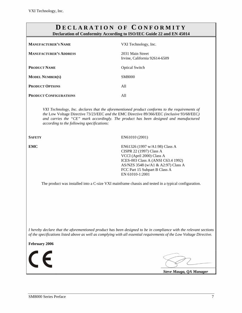
D E C L A R A T I O N O F C O N F O R M I T Y Declaration of Conformity According to ISO/IEC Guide 22 and EN 45014
MANUFACTURER’S NAME VXI Technology, Inc. MANUFACTURER’S ADDRESS 2031 Main Street Irvine, California 92614-6509 PRODUCT NAME Optical Switch MODEL NUMBER(S) SM8000 PRODUCT OPTIONS All PRODUCT CONFIGURATIONS All
VXI Technology, Inc. declares that the aforementioned product conforms to the requirements of the Low Voltage Directive 73/23/EEC and the EMC Directive 89/366/EEC (inclusive 93/68/EEC) and carries the “CE” mark accordingly. The product has been designed and manufactured according to the following specifications:
SAFETY EN61010 (2001) EMC EN61326 (1997 w/A1:98) Class A CISPR 22 (1997) Class A VCCI (April 2000) Class A ICES-003 Class A (ANSI C63.4 1992) AS/NZS 3548 (w/A1 & A2:97) Class A FCC Part 15 Subpart B Class A EN 61010-1:2001
The product was installed into a C-size VXI mainframe chassis and tested in a typical configuration. I hereby declare that the aforementioned product has been designed to be in compliance with the relevant sections of the specifications listed above as well as complying with all essential requirements of the Low Voltage Directive. February 2006
Steve Mauga, QA Manager

VXI Technology, Inc.
8 SM8000 Series Preface
VXI Technology, Inc.
SM8000 Series Preface 9
GENERAL SAFETY INSTRUCTIONS
Review the following safety precautions to avoid bodily injury and/or damage to the product. These precautions must be observed during all phases of operation or service of this product. Failure to comply with these precautions, or with specific warnings elsewhere in this manual, violates safety standards of design, manufacture, and intended use of the product. Service should only be performed by qualified personnel.
TERMS AND SYMBOLS
These terms may appear in this manual: WARNING Indicates that a procedure or condition may cause bodily injury or death. CAUTION Indicates that a procedure or condition could possibly cause damage to
equipment or loss of data. These symbols may appear on the product:
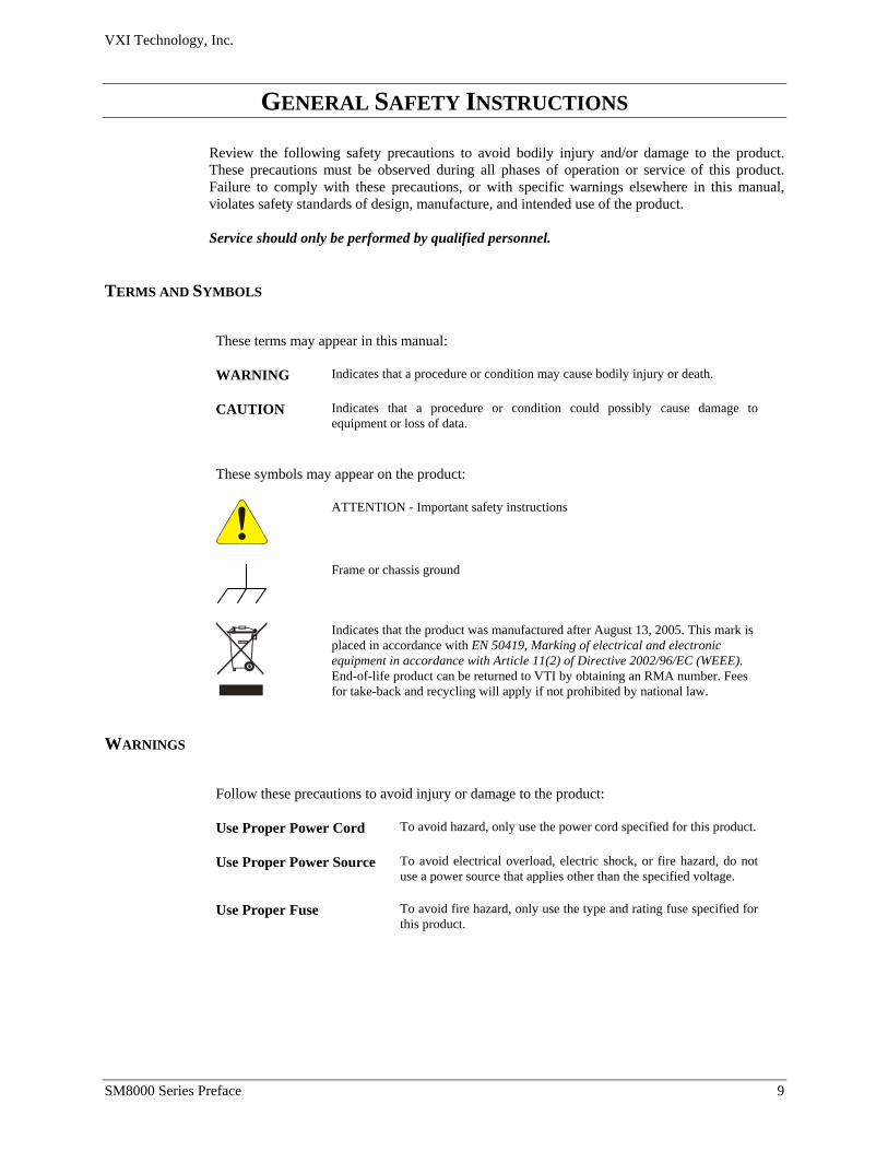
ATTENTION - Important safety instructions
Frame or chassis ground
Indicates that the product was manufactured after August 13, 2005. This mark is placed in accordance with EN 50419, Marking of electrical and electronic equipment in accordance with Article 11(2) of Directive 2002/96/EC (WEEE). End-of-life product can be returned to VTI by obtaining an RMA number. Fees for take-back and recycling will apply if not prohibited by national law.
WARNINGS
Follow these precautions to avoid injury or damage to the product: Use Proper Power Cord To avoid hazard, only use the power cord specified for this product. Use Proper Power Source To avoid electrical overload, electric shock, or fire hazard, do not
use a power source that applies other than the specified voltage. Use Proper Fuse To avoid fire hazard, only use the type and rating fuse specified for
this product.
VXI Technology, Inc.
10 SM8000 Series Preface
WARNINGS (CONT.) Avoid Electric Shock To avoid electric shock or fire hazard, do not operate this product
with the covers removed. Do not connect or disconnect any cable, probes, test leads, etc. while they are connected to a voltage source. Remove all power and unplug unit before performing any service. Service should only be performed by qualified personnel.
Ground the Product This product is grounded through the grounding conductor of the
power cord. To avoid electric shock, the grounding conductor must be connected to earth ground.
Operating Conditions To avoid injury, electric shock or fire hazard: - Do not operate in wet or damp conditions. - Do not operate in an explosive atmosphere. - Operate or store only in specified temperature range. - Provide proper clearance for product ventilation to prevent
overheating. - DO NOT operate if any damage to this product is suspected.
Product should be inspected or serviced only by qualified personnel.
Improper Use The operator of this instrument is advised that if the equipment is used in a manner not specified in this manual, the protection provided by the equipment may be impaired. Conformity is checked by inspection.

VXI Technology, Inc.
SM8000 Series Preface 11
SUPPORT RESOURCES
Support resources for this product are available on the Internet and at VTI Instruments customer support centers. VTI Instruments Corp. World Headquarters VTI Instruments Corp. 2031 Main Street Irvine, CA 92614-6509 Phone: (949) 955-1894 Fax: (949) 955-3041 VTI Instruments Cleveland Instrument Division 5425 Warner Road Suite 13 Valley View, OH 44125 Phone: (216) 447-8950 Fax: (216) 447-8951 VTI Instruments Lake Stevens Instrument Division 3216 Wetmore Avenue, Suite 1 Everett, WA 98201 Phone: (949) 955-1894 Fax: (949) 955-3041 VTI Instruments, Pvt. Ltd. Bangalore Instrument Division 642, 80 Feet Road Koramangala IV Block Bangalore – 560 034 India Phone: +91 80 4040 7900 Phone: +91 80 4162 0200 Fax: +91 80 4170 0200 Technical Support Phone: (949) 955-1894 Fax: (949) 955-3041 E-mail: [email protected]
Visit http://www.vtiinstruments.com for worldwide support sites and service plan information.

VXI Technology, Inc.
12 SM8000 Series Preface
VXI Technology, Inc.
SM8000 Series Introduction 13
SECTION 1
INTRODUCTION OVERVIEW
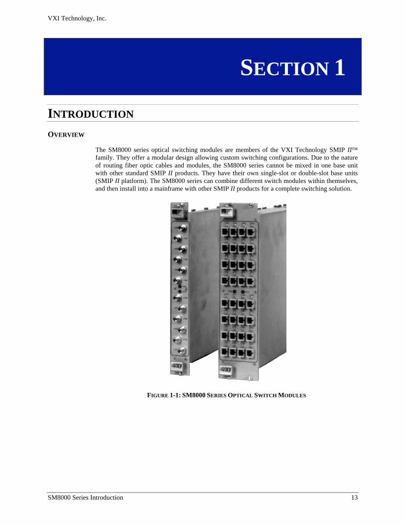
The SM8000 series optical switching modules are members of the VXI Technology SMIP II™ family. They offer a modular design allowing custom switching configurations. Due to the nature of routing fiber optic cables and modules, the SM8000 series cannot be mixed in one base unit with other standard SMIP II products. They have their own single-slot or double-slot base units (SMIP II platform). The SM8000 series can combine different switch modules within themselves, and then install into a mainframe with other SMIP II products for a complete switching solution.
FIGURE 1-1: SM8000 SERIES OPTICAL SWITCH MODULES
VXI Technology, Inc.
14 SM8000 Series Introduction
SM8000 SERIES - OPTICAL SWITCH CONTROLLER
The SM8000 high-density optical switch controller module is designed to handle many different combinations of optical switching modules. This includes up to 12 single mode prism switches, or 4 multi-switch modules of various configurations, or 4 variable attenuators or tunable filters. The optical modules may be mixed and matched on a single SM8000. Please contact VXI Technology, Inc. directly for available configurations. The SM8000 was designed to mount into either a single or double-slot VXI instrument carrier. The selection of the size of the carrier is dependent on the optical modules that are being controlled by the SM8000.
VXI Technology, Inc.
SM8000 Series Introduction 15
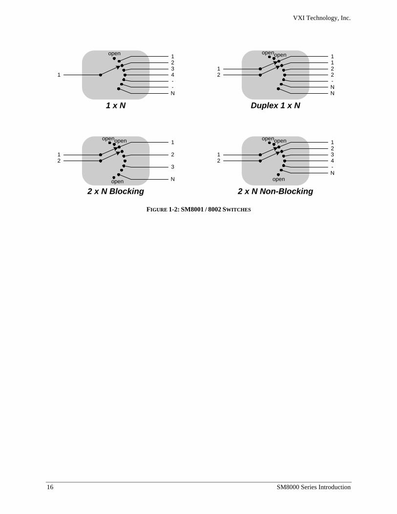
SM8001 / SM8002 - MULTI-CHANNEL SWITCHES
The SM8001 and SM8002 base units house the 1xN and 2xN multi-channel switches. They each hold up to four optical switch modules. Each switch module can be either a 1xN (where N ranges from 1 to 32) or a 2xN (where N ranges from 2 to 30). The SM8001 is a single-slot base unit, or platform, while the SM8002 is a double-slot base unit. Configurations
The following configurations are available for the SM8001 and SM8002: SM8001 and SM8002 - Multi-channel Switches: 1 x N Duplex 1 x N 2 x N Blocking 2 x N Non-Blocking The total number of available connectors per base unit is: SM8001 Single-Slot, Multi-channel Base Unit: 12 ST connectors 16 SC connectors 12 FC connectors SM8002 Double-slot, Multi-channel Base Unit: 24 ST connectors 32 SC connectors 24 FC connectors
VXI Technology, Inc.
16 SM8000 Series Introduction
1
1234--N
open
1 x N
2
1122-NN
openopen
1
Duplex 1 x N
2
1
2
3
N
openopen
1
open
2 x N Blocking
2
1234-N
openopen
1
open
2 x N Non-Blocking
FIGURE 1-2: SM8001 / 8002 SWITCHES
VXI Technology, Inc.
SM8000 Series Introduction 17
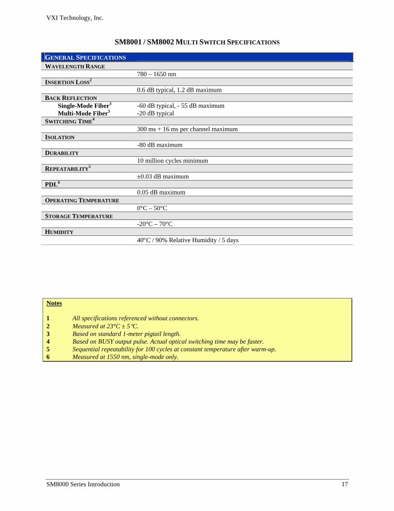
SM8001 / SM8002 MULTI SWITCH SPECIFICATIONS
GENERAL SPECIFICATIONS WAVELENGTH RANGE 780 – 1650 nm INSERTION LOSS2 0.6 dB typical, 1.2 dB maximum BACK REFLECTION Single-Mode Fiber3 Multi-Mode Fiber3
-60 dB typical, - 55 dB maximum -20 dB typical
SWITCHING TIME4 300 ms + 16 ms per channel maximum ISOLATION -80 dB maximum DURABILITY 10 million cycles minimum REPEATABILITY5 ±0.03 dB maximum PDL6 0.05 dB maximum OPERATING TEMPERATURE 0°C – 50°C STORAGE TEMPERATURE -20°C – 70°C HUMIDITY 40°C / 90% Relative Humidity / 5 days
Notes 1 All specifications referenced without connectors. 2 Measured at 23°C ± 5°C. 3 Based on standard 1-meter pigtail length. 4 Based on BUSY output pulse. Actual optical switching time may be faster. 5 Sequential repeatability for 100 cycles at constant temperature after warm-up. 6 Measured at 1550 nm, single-mode only.
VXI Technology, Inc.
18 SM8000 Series Introduction
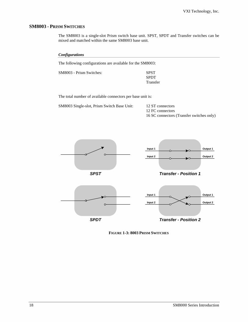
SM8003 - PRISM SWITCHES
The SM8003 is a single-slot Prism switch base unit. SPST, SPDT and Transfer switches can be mixed and matched within the same SM8003 base unit. Configurations
The following configurations are available for the SM8003: SM8003 - Prism Switches: SPST SPDT Transfer The total number of available connectors per base unit is: SM8003 Single-slot, Prism Switch Base Unit: 12 ST connectors 12 FC connectors 16 SC connectors (Transfer switches only)
SPST
SPDT
Transfer - Position 1
Output 2
Output 1Input 1
Input 2
Transfer - Position 2
Output 2
Output 1Input 1
Input 2
FIGURE 1-3: 8003 PRISM SWITCHES
VXI Technology, Inc.
SM8000 Series Introduction 19
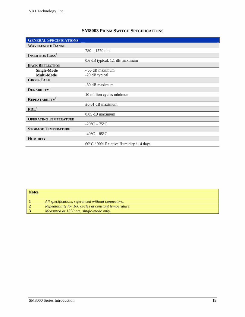
SM8003 PRISM SWITCH SPECIFICATIONS
GENERAL SPECIFICATIONS WAVELENGTH RANGE 780 – 1570 nm INSERTION LOSS2 0.6 dB typical, 1.1 dB maximum BACK REFLECTION Single-Mode Multi-Mode
- 55 dB maximum -20 dB typical
CROSS-TALK -80 dB maximum DURABILITY 10 million cycles minimum REPEATABILITY2 ±0.01 dB maximum PDL3 0.05 dB maximum OPERATING TEMPERATURE -20°C – 75°C STORAGE TEMPERATURE -40°C – 85°C HUMIDITY 60°C / 90% Relative Humidity / 14 days
Notes 1 All specifications referenced without connectors. 2 Repeatability for 100 cycles at constant temperature. 3 Measured at 1550 nm, single-mode only.
VXI Technology, Inc.
20 SM8000 Series Introduction
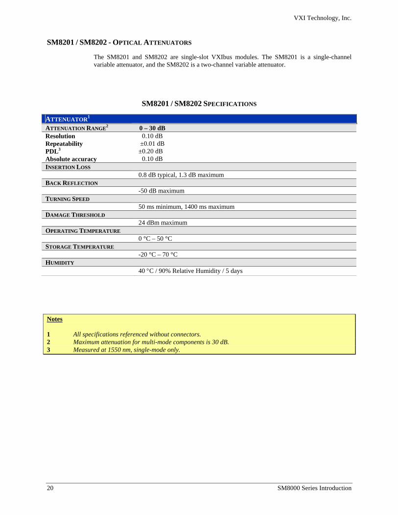
SM8201 / SM8202 - OPTICAL ATTENUATORS
The SM8201 and SM8202 are single-slot VXIbus modules. The SM8201 is a single-channel variable attenuator, and the SM8202 is a two-channel variable attenuator.
SM8201 / SM8202 SPECIFICATIONS
ATTENUATOR1 ATTENUATION RANGE2 0 – 30 dB Resolution Repeatability PDL3 Absolute accuracy
0.10 dB ±0.01 dB ±0.20 dB 0.10 dB
INSERTION LOSS 0.8 dB typical, 1.3 dB maximum BACK REFLECTION -50 dB maximum TURNING SPEED 50 ms minimum, 1400 ms maximum DAMAGE THRESHOLD 24 dBm maximum OPERATING TEMPERATURE 0 °C – 50 °C STORAGE TEMPERATURE -20 °C – 70 °C HUMIDITY 40 °C / 90% Relative Humidity / 5 days
Notes 1 All specifications referenced without connectors. 2 Maximum attenuation for multi-mode components is 30 dB. 3 Measured at 1550 nm, single-mode only.
VXI Technology, Inc.
SM8000 Series Preparation for Use 21
SECTION 2
PREPARATION FOR USE INTRODUCTION
When the SMIP II is unpacked from its shipping carton, the contents should include the following items:
(1) SMIP II VXIbus module (1) SM8000 Series Optical Switch User’s Manual (this manual)
All components should be immediately inspected for damage upon receipt of the unit. Once the SMIP II is assessed to be in good condition, it may be installed into an appropriate C-size or D-size VXIbus chassis in any slot other than slot zero. The chassis should be checked to ensure that it is capable of providing adequate power and cooling for the SMIP II. Once the chassis is found adequate, the SMIP’s logical address and the chassis’ backplane jumpers should be configured prior to the SMIP’s installation.
CALCULATING SYSTEM POWER AND COOLING REQUIREMENTS
It is imperative that the chassis provide adequate power and cooling for this module. Referring to the chassis user’s manual, confirm that the power budget for the system (the chassis and all modules installed therein) is not exceeded and that the cooling system can provide adequate airflow at the specified backpressure. It should be noted that if the chassis cannot provide adequate power to the module, the instrument may not perform to specification or possibly not operate at all. In addition, if adequate cooling is not provided, the reliability of the instrument will be jeopardized and permanent damage may occur. Damage found to have occurred due to inadequate cooling would also void the warranty of the module.
SETTING THE CHASSIS BACKPLANE JUMPERS
Please refer to the chassis operation manual for further details on setting the backplane jumpers.
VXI Technology, Inc.
22 SM8000 Series Preparation for Use
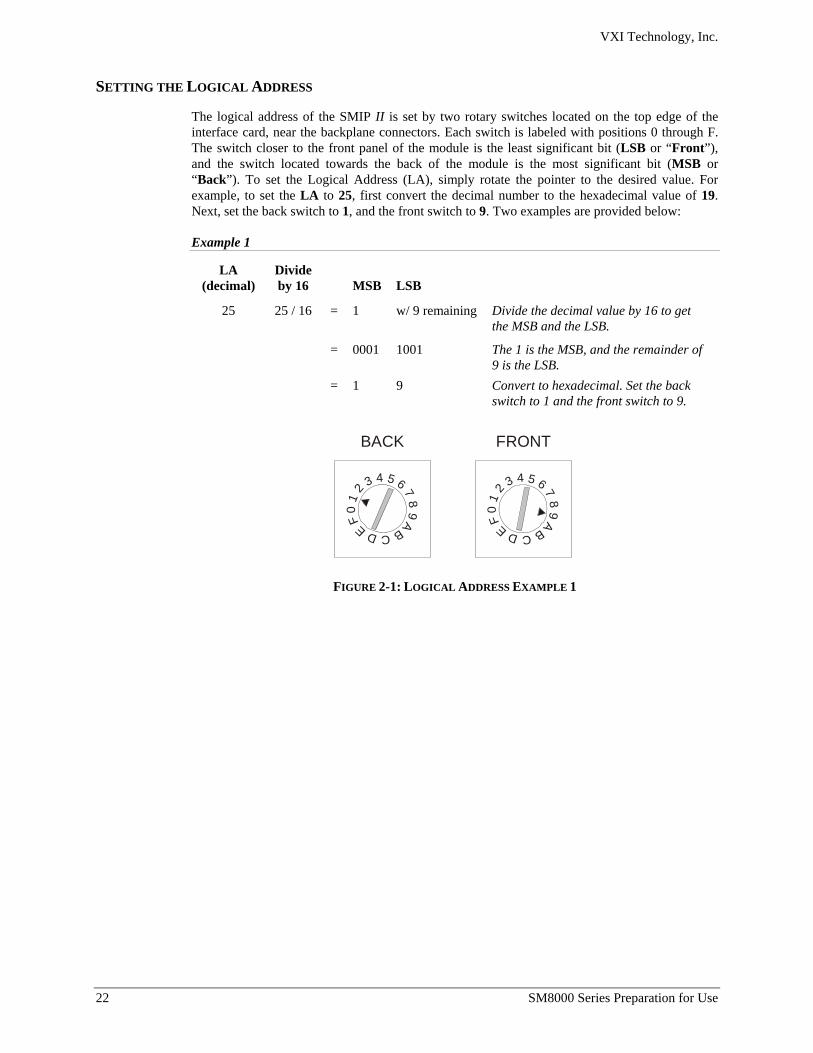
SETTING THE LOGICAL ADDRESS
The logical address of the SMIP II is set by two rotary switches located on the top edge of the interface card, near the backplane connectors. Each switch is labeled with positions 0 through F. The switch closer to the front panel of the module is the least significant bit (LSB or “Front”), and the switch located towards the back of the module is the most significant bit (MSB or “Back”). To set the Logical Address (LA), simply rotate the pointer to the desired value. For example, to set the LA to 25, first convert the decimal number to the hexadecimal value of 19. Next, set the back switch to 1, and the front switch to 9. Two examples are provided below: Example 1
LA (decimal)
Divide by 16 MSB LSB
25 25 / 16 = 1 w/ 9 remaining Divide the decimal value by 16 to get the MSB and the LSB.
= 0001 1001 The 1 is the MSB, and the remainder of 9 is the LSB.
= 1 9 Convert to hexadecimal. Set the back switch to 1 and the front switch to 9.
0 1
2 3 4 5 6 7 8 9 A B C D E F
0 1
2 3 4 5 6 7 89 A B C D E F
BACK FRONT
FIGURE 2-1: LOGICAL ADDRESS EXAMPLE 1
VXI Technology, Inc.
SM8000 Series Preparation for Use 23
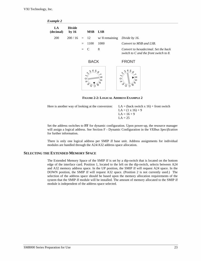
Example 2
LA (decimal)
Divide by 16 MSB LSB
200 200 / 16 = 12 w/ 8 remaining Divide by 16.
= 1100 1000 Convert to MSB and LSB.
= C 8 Convert to hexadecimal. Set the back switch to C and the front switch to 8.
0 1
2 3 4 5 6 7 8 9 A B C D E F
0 1
2 3 4 5 6 7 8 9 A B C D E F
BACK FRONT
FIGURE 2-2: LOGICAL ADDRESS EXAMPLE 2
Here is another way of looking at the conversion: LA = (back switch x 16) + front switch LA = (1 x 16) + 9 LA = 16 + 9 LA = 25 Set the address switches to FF for dynamic configuration. Upon power-up, the resource manager will assign a logical address. See Section F - Dynamic Configuration in the VXIbus Specification for further information. There is only one logical address per SMIP II base unit. Address assignments for individual modules are handled through the A24/A32 address space allocation.
SELECTING THE EXTENDED MEMORY SPACE
The Extended Memory Space of the SMIP II is set by a dip-switch that is located on the bottom edge of the interface card. Position 1, located to the left on the dip-switch, selects between A24 and A32 memory address space. In the UP position, the SMIP II will request A24 space. In the DOWN position, the SMIP II will request A32 space. (Position 2 is not currently used.) The selection of the address space should be based upon the memory allocation requirements of the system that the SMIP II module will be installed. The amount of memory allocated to the SMIP II module is independent of the address space selected.
VXI Technology, Inc.
24 SM8000 Series Preparation for Use
OPTICAL CONNECTIONS
The SM8000 series are all shipped with dust caps over each optical connector. These dust caps should remain in place at all times while the instrument is not in use. Cleaning Optical Connectors
1. Clean both connectors to remove any dirt or particles, which could decrease performance or permanently damage the connector.
a) Using high-grade isopropyl alcohol (or equivalent) dampen a cotton swab and shake off
any excess alcohol before cleaning. The cotton swab should be moist but not wet. b) Gently clean the surface of the connector and around the connector ferrule. c) Allow the connectors to dry for at least one minute.
Service should only be performed by qualified personnel.
Mating Optical Connectors
1. Smoothly insert the appropriate connector ferrule into the adapter taking caution not to allow the fiber tip to make contact with any surface. If this happens, re-clean the connector and start again.
2. Tighten the connector finger-tight; do not over-tighten. If the loss is unacceptable, remove the
connector, re-clean both connectors and start again. These steps may need to be repeated several times before a low-loss connection is made.
3. After the connection is made, monitor the stability of the optical throughput for a few minutes
until stable. If the loss is unacceptable, re-clean the connectors and start again.
VXI Technology, Inc.
SM8000 Series Operation 25
SECTION 3
OPERATION GENERAL DESCRIPTION
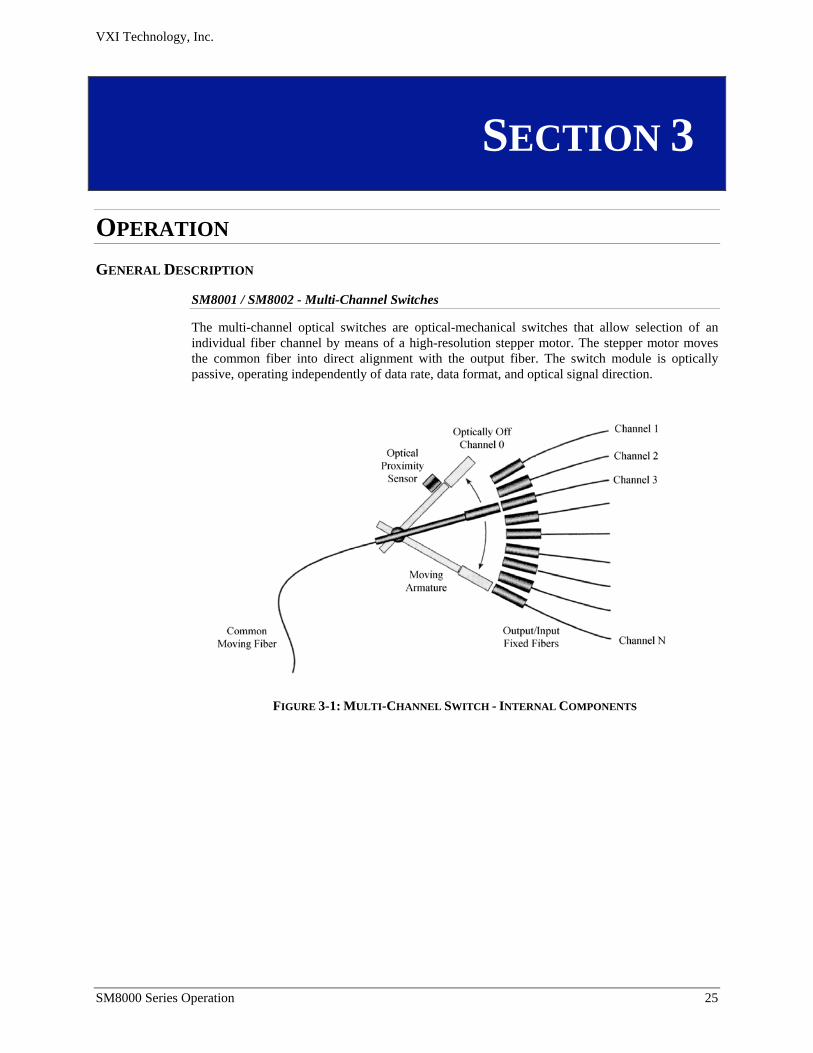
SM8001 / SM8002 - Multi-Channel Switches
The multi-channel optical switches are optical-mechanical switches that allow selection of an individual fiber channel by means of a high-resolution stepper motor. The stepper motor moves the common fiber into direct alignment with the output fiber. The switch module is optically passive, operating independently of data rate, data format, and optical signal direction.
FIGURE 3-1: MULTI-CHANNEL SWITCH - INTERNAL COMPONENTS
VXI Technology, Inc.
26 SM8000 Series Operation
SM8003 - Prism Switches
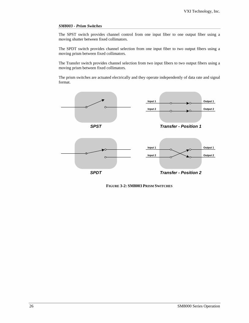
The SPST switch provides channel control from one input fiber to one output fiber using a moving shutter between fixed collimators. The SPDT switch provides channel selection from one input fiber to two output fibers using a moving prism between fixed collimators. The Transfer switch provides channel selection from two input fibers to two output fibers using a moving prism between fixed collimators. The prism switches are actuated electrically and they operate independently of data rate and signal format.
SPST
SPDT
Transfer - Position 1
Output 2
Output 1Input 1
Input 2
Transfer - Position 2
Output 2
Output 1Input 1
Input 2
FIGURE 3-2: SM8003 PRISM SWITCHES
VXI Technology, Inc.
SM8000 Series Operation 27
SM8201 / SM8202 - Optical Attenuators
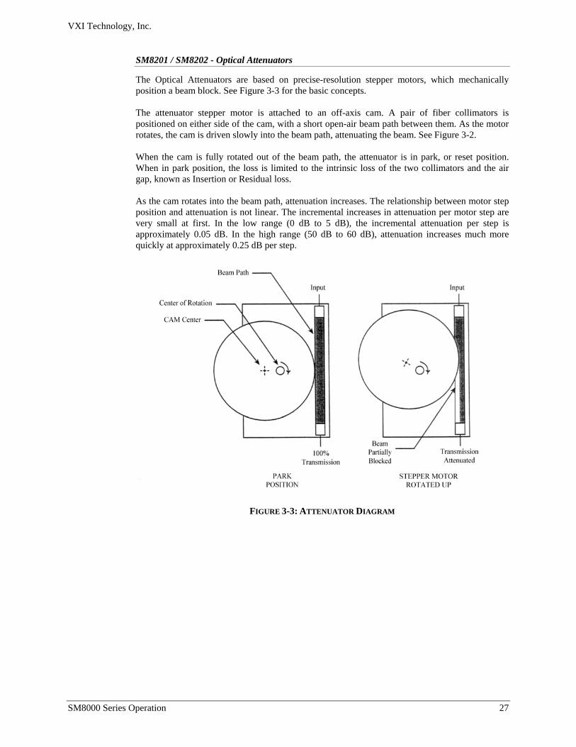
The Optical Attenuators are based on precise-resolution stepper motors, which mechanically position a beam block. See Figure 3-3 for the basic concepts. The attenuator stepper motor is attached to an off-axis cam. A pair of fiber collimators is positioned on either side of the cam, with a short open-air beam path between them. As the motor rotates, the cam is driven slowly into the beam path, attenuating the beam. See Figure 3-2. When the cam is fully rotated out of the beam path, the attenuator is in park, or reset position. When in park position, the loss is limited to the intrinsic loss of the two collimators and the air gap, known as Insertion or Residual loss. As the cam rotates into the beam path, attenuation increases. The relationship between motor step position and attenuation is not linear. The incremental increases in attenuation per motor step are very small at first. In the low range (0 dB to 5 dB), the incremental attenuation per step is approximately 0.05 dB. In the high range (50 dB to 60 dB), attenuation increases much more quickly at approximately 0.25 dB per step.
FIGURE 3-3: ATTENUATOR DIAGRAM

VXI Technology, Inc.
28 SM8000 Series Operation
OPERATION
SM8001 / SM8002 - Multi-Channel Switches
When controlling multi-switch modules, the operation is quite similar to that of any other SMIP II family product, but the data sent is operated on a little bit differently. The SM8000 must be configured to control the multi-switch device on one of four ports. This is done at the factory with hardware selectable jumpers. Once configured for multi-switch operation, the control of the switch is accomplished by writing to the appropriate Relay Register. Relay registers 02 through 08 are used to control the multi-switch modules. The value written to the multi-switch module is dependent on the type/size of the switch. For example, if the switch is a 1xN switch, writing the value of 00h to Relay Register 02 would optically connect the switches input to the first output. A write of 0Ah would connect the input to the 11th output, and so on. Data lines 4 through 0 are used to transfer data to the switch modules. The Busy signal from the optical module may be monitored to indicate when the optical module has completed moving to the commanded switch setting. The optical module also generates an Error signal that may be monitored. This signal might be used to provide a confidence check that the module is being controlled properly. Resetting the Switch
When the switch is in reset (park) position, channel zero, or optical off, there is no optical connection to any output channel. Set the switch to the reset position to prevent optical data from passing through the switch, or to reset the stepper motor. During a reset operation, optical noise may appear on various output channels as the armature rotates. There are two ways to reset the switch. The first is to cycle power to return the switch to the reset position. The second is to return the switch to the reset position using a sequence of writes to the SMIP module rather than interrupting the supply power. See the example of a multi-switch reset write sequence as described later in this manual. The BUSY output remains high until the reset operation is complete and the device is ready to receive additional instructions. Relay Registers - Output Channel Selection
The following sections show information to select channels for the SM8001/8002 through the relay registers. Each configuration section includes an optical input/output relation figure, followed by a table that lists the control codes for channel selection.
VXI Technology, Inc.
SM8000 Series Operation 29
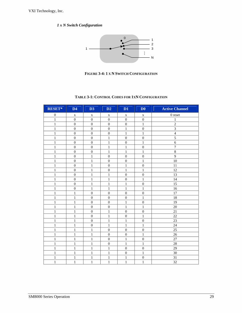
1 x N Switch Configuration
1
123
N
0
...
FIGURE 3-4: 1 X N SWITCH CONFIGURATION
TABLE 3-1: CONTROL CODES FOR 1XN CONFIGURATION
RESET* D4 D3 D2 D1 D0 Active Channel 0 x x x x x 0 reset 1 0 0 0 0 0 1 1 0 0 0 0 1 2 1 0 0 0 1 0 3 1 0 0 0 1 1 4 1 0 0 1 0 0 5 1 0 0 1 0 1 6 1 0 0 1 1 0 7 1 0 0 1 1 1 8 1 0 1 0 0 0 9 1 0 1 0 0 1 10 1 0 1 0 1 0 11 1 0 1 0 1 1 12 1 0 1 1 0 0 13 1 0 1 1 0 1 14 1 0 1 1 1 0 15 1 0 1 1 1 1 16 1 1 0 0 0 0 17 1 1 0 0 0 1 18 1 1 0 0 1 0 19 1 1 0 0 1 1 20 1 1 0 1 0 0 21 1 1 0 1 0 1 22 1 1 0 1 1 0 23 1 1 0 1 1 1 24 1 1 1 0 0 0 25 1 1 1 0 0 1 26 1 1 1 0 1 0 27 1 1 1 0 1 1 28 1 1 1 1 0 0 29 1 1 1 1 0 1 30 1 1 1 1 1 0 31 1 1 1 1 1 1 32
VXI Technology, Inc.
30 SM8000 Series Operation
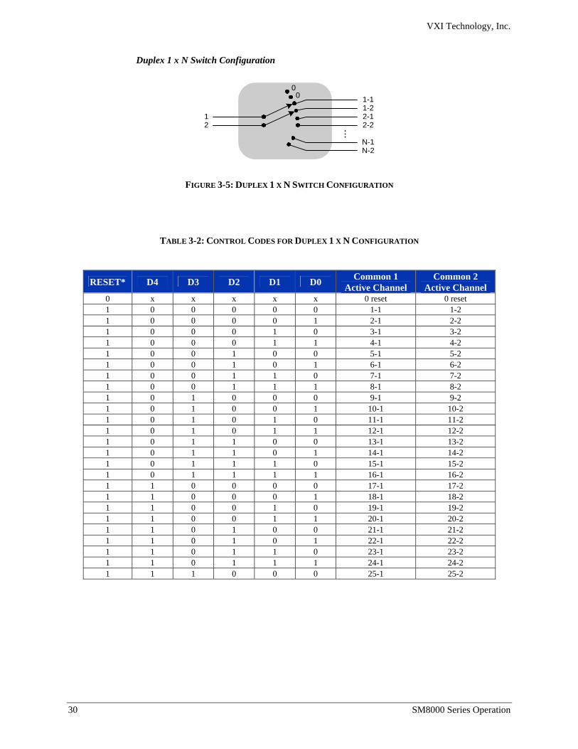
Duplex 1 x N Switch Configuration
2
1-11-22-12-2
N-1N-2
00
1...
FIGURE 3-5: DUPLEX 1 X N SWITCH CONFIGURATION
TABLE 3-2: CONTROL CODES FOR DUPLEX 1 X N CONFIGURATION
RESET* D4 D3 D2 D1 D0 Common 1 Active Channel
Common 2 Active Channel
0 x x x x x 0 reset 0 reset 1 0 0 0 0 0 1-1 1-2 1 0 0 0 0 1 2-1 2-2 1 0 0 0 1 0 3-1 3-2 1 0 0 0 1 1 4-1 4-2 1 0 0 1 0 0 5-1 5-2 1 0 0 1 0 1 6-1 6-2 1 0 0 1 1 0 7-1 7-2 1 0 0 1 1 1 8-1 8-2 1 0 1 0 0 0 9-1 9-2 1 0 1 0 0 1 10-1 10-2 1 0 1 0 1 0 11-1 11-2 1 0 1 0 1 1 12-1 12-2 1 0 1 1 0 0 13-1 13-2 1 0 1 1 0 1 14-1 14-2 1 0 1 1 1 0 15-1 15-2 1 0 1 1 1 1 16-1 16-2 1 1 0 0 0 0 17-1 17-2 1 1 0 0 0 1 18-1 18-2 1 1 0 0 1 0 19-1 19-2 1 1 0 0 1 1 20-1 20-2 1 1 0 1 0 0 21-1 21-2 1 1 0 1 0 1 22-1 22-2 1 1 0 1 1 0 23-1 23-2 1 1 0 1 1 1 24-1 24-2 1 1 1 0 0 0 25-1 25-2
VXI Technology, Inc.
SM8000 Series Operation 31
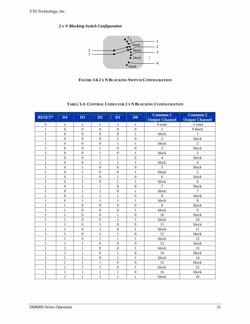
2 x N Blocking Switch Configuration
1
1
2
3
N
0-1
2
block
block
block
block
...
FIGURE 3-6 2 X N BLOCKING SWITCH CONFIGURATION
TABLE 3-3: CONTROL CODES FOR 2 X N BLOCKING CONFIGURATION
RESET* D4 D3 D2 D1 D0 Common 1 Output Channel
Common 2 Output Channel
0 x x x x x 0 reset -1 reset 1 0 0 0 0 0 1 0 block 1 0 0 0 0 1 block 1 1 0 0 0 1 0 2 block 1 0 0 0 1 1 block 2 1 0 0 1 0 0 3 block 1 0 0 1 0 1 block 3 1 0 0 1 1 0 4 block 1 0 0 1 1 1 block 4 1 0 1 0 0 0 5 block 1 0 1 0 0 1 block 5 1 0 1 0 1 0 6 block 1 0 1 0 1 1 block 6 1 0 1 1 0 0 7 block 1 0 1 1 0 1 block 7 1 0 1 1 1 0 8 block 1 0 1 1 1 1 block 8 1 1 0 0 0 0 9 block 1 1 0 0 0 1 block 9 1 1 0 0 1 0 10 block 1 1 0 0 1 1 block 10 1 1 0 1 0 0 11 block 1 1 0 1 0 1 block 11 1 1 0 1 1 0 12 block 1 1 0 1 1 1 block 12 1 1 1 0 0 0 13 block 1 1 1 0 0 1 block 13 1 1 1 0 1 0 14 block 1 1 1 0 1 1 block 14 1 1 1 1 0 0 15 block 1 1 1 1 0 1 block 15 1 1 1 1 1 0 16 block 1 1 1 1 1 1 block 16
VXI Technology, Inc.
32 SM8000 Series Operation
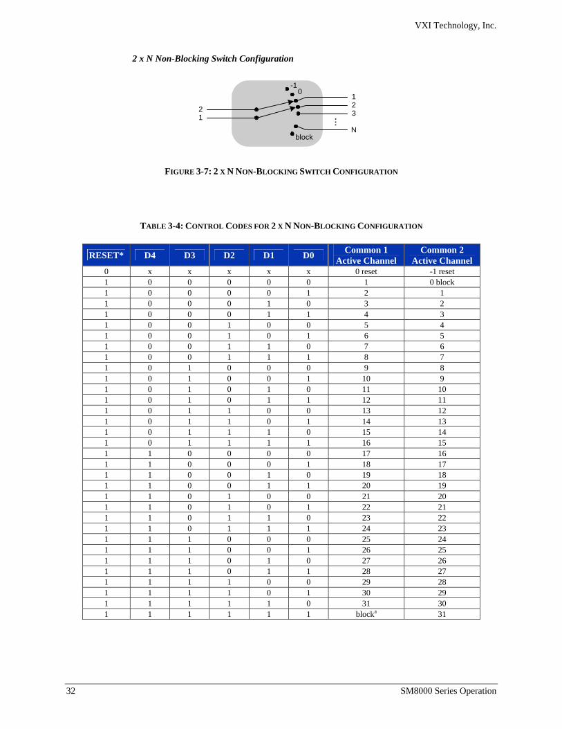
2 x N Non-Blocking Switch Configuration
1
123
N
0
2
block
...
-1
FIGURE 3-7: 2 X N NON-BLOCKING SWITCH CONFIGURATION
TABLE 3-4: CONTROL CODES FOR 2 X N NON-BLOCKING CONFIGURATION
RESET* D4 D3 D2 D1 D0 Common 1 Active Channel
Common 2 Active Channel
0 x x x x x 0 reset -1 reset 1 0 0 0 0 0 1 0 block 1 0 0 0 0 1 2 1 1 0 0 0 1 0 3 2 1 0 0 0 1 1 4 3 1 0 0 1 0 0 5 4 1 0 0 1 0 1 6 5 1 0 0 1 1 0 7 6 1 0 0 1 1 1 8 7 1 0 1 0 0 0 9 8 1 0 1 0 0 1 10 9 1 0 1 0 1 0 11 10 1 0 1 0 1 1 12 11 1 0 1 1 0 0 13 12 1 0 1 1 0 1 14 13 1 0 1 1 1 0 15 14 1 0 1 1 1 1 16 15 1 1 0 0 0 0 17 16 1 1 0 0 0 1 18 17 1 1 0 0 1 0 19 18 1 1 0 0 1 1 20 19 1 1 0 1 0 0 21 20 1 1 0 1 0 1 22 21 1 1 0 1 1 0 23 22 1 1 0 1 1 1 24 23 1 1 1 0 0 0 25 24 1 1 1 0 0 1 26 25 1 1 1 0 1 0 27 26 1 1 1 0 1 1 28 27 1 1 1 1 0 0 29 28 1 1 1 1 0 1 30 29 1 1 1 1 1 0 31 30 1 1 1 1 1 1 blocka 31
VXI Technology, Inc.
SM8000 Series Operation 33
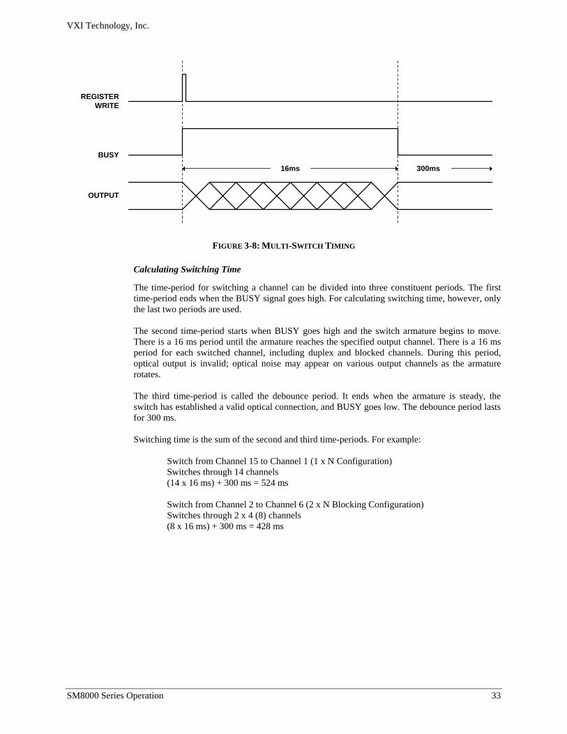
REGISTERWRITE
BUSY
OUTPUT
300ms16ms
FIGURE 3-8: MULTI-SWITCH TIMING
Calculating Switching Time
The time-period for switching a channel can be divided into three constituent periods. The first time-period ends when the BUSY signal goes high. For calculating switching time, however, only the last two periods are used. The second time-period starts when BUSY goes high and the switch armature begins to move. There is a 16 ms period until the armature reaches the specified output channel. There is a 16 ms period for each switched channel, including duplex and blocked channels. During this period, optical output is invalid; optical noise may appear on various output channels as the armature rotates. The third time-period is called the debounce period. It ends when the armature is steady, the switch has established a valid optical connection, and BUSY goes low. The debounce period lasts for 300 ms. Switching time is the sum of the second and third time-periods. For example:
Switch from Channel 15 to Channel 1 (1 x N Configuration) Switches through 14 channels (14 x 16 ms) + 300 ms = 524 ms Switch from Channel 2 to Channel 6 (2 x N Blocking Configuration) Switches through 2 x 4 (8) channels (8 x 16 ms) + 300 ms = 428 ms
VXI Technology, Inc.
34 SM8000 Series Operation
SM8003 - Prism Switches
When controlling single mode prism switches the operation of the SM8000 is also similar to that of any other SMIP II family product. The switches are directly controlled by register writes to the Relay Register. See Writing to the Relay Register in the Programming section for a detailed explanation of this type of operation. Only relay register 00h is used to control the prism switches. SM8201 / SM8202 - Optical Attenuators
The attenuator modules are internally controlled via an I2C bus interface. Operation of this type of module is accomplished by loading the proper command and attenuator data information into the proper registers inside the SM8000. The SM8000 must be configured to control the attenuator modules on one of four ports. These same ports are used for the multi-switch devices. This is done at the factory with hardware selectable jumpers. Once configured for attenuator module operation, the control of the attenuator module consists of writing the control word and the attenuator data word to the SM8000. This operation is more fully discussed in the Programming section of this manual. Once the Relay Register (02 through 08) has been configured to control an attenuator, and has been written to, the command sequence is initiated and the module begins to move to the newly commanded setting. The Busy signal from the optical module may be monitored to indicate when the optical module has finished moving to the commanded attenuation. The optical module also generates an Error signal that may be monitored. This signal might be used to provide a confidence check that the module is being controlled properly.
VXI Technology, Inc.
SM8000 Series Operation 35
Starting the Device
The device resets upon application of power. The Optical Attenuators park at the minimum-loss position. Control Modes
The Optical Attenuators can be operated in two modes: uncalibrated and calibrated. The uncalibrated mode is called Move-To-Absolute-Step mode. In this mode, the user sends movement requests to the internal stepping motor through the Move-To-Absolute-Step interface. The internal stepping motor responds by moving one step up, or one step down as requested. In this mode, there is no conversion of step number to absolute attenuation. Move-To-Absolute-Step is the simplest mode of operation. This method of operation is typically used when devices are used in a feedback loop to maintain a particular attenuation regardless of absolute position. The calibrated, absolute conversion mode of operation sends absolute attenuation requests to the Optical Attenuator. The circuitry then translates the commanded absolute request into a motor-step position and rotates the motor accordingly. This method of operation is typically used when the devices are used to calibrate other devices, or to set absolute references within a system. Both modes of operation are described in detail in the following sections. Uncalibrated Operation - Move-To-Absolute-Step
The motorized Optical Attenuators are all based on stepping motor technology. The easiest method of using these devices is to simply command the motor to step in one direction, or the other. For our purposes, stepping will increase attenuation, while stepping down will decrease attenuation. To utilize this mode of operation, simply command the Optical Attenuator to Move-To-Absolute-Step. See the Attenuator Command Set in the Programming section. Calibrated Operation
The Optical Attenuators are all based on stepping motor technology. Operating in the calibrated mode requires use of the I2C interface on the optical modules. The I2C interface is a linearized controller, allowing users to select for the attenuator, he absolute attenuation in dB. It is also possible to command uncalibrated step movements while operating in calibrated mode. Note that following an uncalibrated step, a Query Attenuation command will return invalid data. A subsequent calibrated movement will restore query command validity.
VXI Technology, Inc.
36 SM8000 Series Operation
BUSY Signal
The BUSY bit is driven high by the device whenever a Set Attenuation command is received, or when a RESET signal is received. The BUSY signal remains high whenever a command is executed and the stepper motor is moving. During this time, no other commands should be sent to the device, as this may corrupt the internal state of the device requiring a RESET to clear. ERROR Status
The ERROR bit is driven high by the device whenever an Out of Range error, or a RESET error is detected. RESET errors occur when the unit does not find its Park position correctly, and may indicate a hardware problem. Resetting the Device
See the RESET commands in the Programming section. Commanding the Devices
Step 1 - Power Up and Initialize The device will reset when power is applied. Step 2 - Query Default Parameters Before using the device in calibrated mode, query to obtain the minimum and maximum absolute attenuation. Use this data to ensure that commands sent are always within range. The commands to gather the device information are: • Query Minimum Attenuation - 82h • Query Maximum Attenuation - 83h Step 3 - Actuate the Device Use the appropriate Set commands and actuate the device. For verification purposes, pick a large change first to ensure proper operation of the device. Very small changes can be requested, however, they can be misleading for test purposes since they are practically undetectable. The command to actuate the device is: • Set Attenuation - 80h
VXI Technology, Inc.
SM8000 Series Programming 37
SECTION 4
PROGRAMMING REGISTER ACCESS
The SMIP II optical modules are VXIbus register-based devices. Register-based programming is a series of reads and writes directly to the switch module registers. This eliminates the time for command parsing thus increasing speed.
ADDRESSING
The VTI switching modules utilize either the A24 or A32 space of the shared-memory architecture. To read or write to a module register, a register address needs to be specified. This is done by using the offset value (assigned by the resource manager) and multiplying it by 256 or 64 k to get the base address in A24 or A32 address space, respectively
A24 Base Address = Offset value * 0x00FF (or 256)
A32 Base Address = Offset value * 0xFFFF (or 65,535)
The A24 or A32 offset value, assigned by the resource manager, can also be accessed by reading the A16 Offset Register. To address the A16 Offset Register use the following formula:
A16 Base Address = (Logical Address * 64) + 0xC000 (or 49,152)
then
A16 Offset Register Address = A16 Base Address + 6 See following for the A16 Memory Map and the A24/A32 address space allocation.
VXI Technology, Inc.
38 SM8000 Series Programming
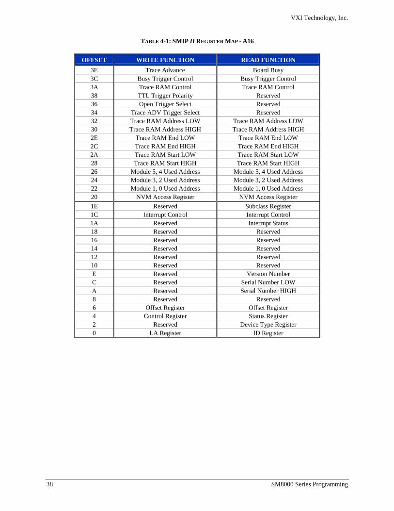
TABLE 4-1: SMIP II REGISTER MAP - A16
OFFSET WRITE FUNCTION READ FUNCTION 3E Trace Advance Board Busy 3C Busy Trigger Control Busy Trigger Control 3A Trace RAM Control Trace RAM Control 38 TTL Trigger Polarity Reserved 36 Open Trigger Select Reserved 34 Trace ADV Trigger Select Reserved 32 Trace RAM Address LOW Trace RAM Address LOW 30 Trace RAM Address HIGH Trace RAM Address HIGH 2E Trace RAM End LOW Trace RAM End LOW 2C Trace RAM End HIGH Trace RAM End HIGH 2A Trace RAM Start LOW Trace RAM Start LOW 28 Trace RAM Start HIGH Trace RAM Start HIGH 26 Module 5, 4 Used Address Module 5, 4 Used Address 24 Module 3, 2 Used Address Module 3, 2 Used Address 22 Module 1, 0 Used Address Module 1, 0 Used Address 20 NVM Access Register NVM Access Register 1E Reserved Subclass Register 1C Interrupt Control Interrupt Control 1A Reserved Interrupt Status 18 Reserved Reserved 16 Reserved Reserved 14 Reserved Reserved 12 Reserved Reserved 10 Reserved Reserved E Reserved Version Number C Reserved Serial Number LOW A Reserved Serial Number HIGH 8 Reserved Reserved 6 Offset Register Offset Register 4 Control Register Status Register 2 Reserved Device Type Register 0 LA Register ID Register
VXI Technology, Inc.
SM8000 Series Programming 39
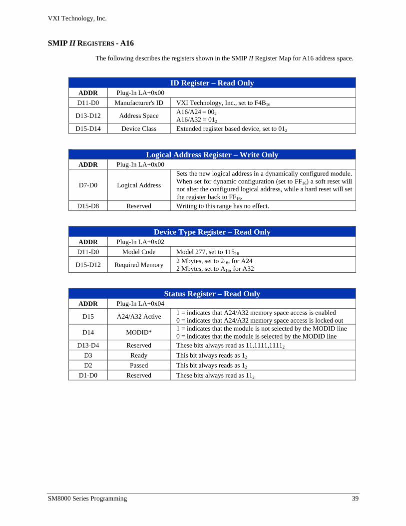
SMIP II REGISTERS - A16
The following describes the registers shown in the SMIP II Register Map for A16 address space.
ID Register – Read Only ADDR Plug-In LA+0x00 D11-D0 Manufacturer's ID VXI Technology, Inc., set to F4B16
D13-D12 Address Space A16/A24 = 002 A16/A32 = 012
D15-D14 Device Class Extended register based device, set to 012
Logical Address Register – Write Only ADDR Plug-In LA+0x00
D7-D0 Logical Address
Sets the new logical address in a dynamically configured module. When set for dynamic configuration (set to FF16) a soft reset will not alter the configured logical address, while a hard reset will set the register back to FF16.
D15-D8 Reserved Writing to this range has no effect.
Device Type Register – Read Only ADDR Plug-In LA+0x02 D11-D0 Model Code Model 277, set to 11516
D15-D12 Required Memory 2 Mbytes, set to 216, for A24 2 Mbytes, set to A16, for A32
Status Register – Read Only ADDR Plug-In LA+0x04
D15 A24/A32 Active 1 = indicates that A24/A32 memory space access is enabled 0 = indicates that A24/A32 memory space access is locked out
D14 MODID* 1 = indicates that the module is not selected by the MODID line 0 = indicates that the module is selected by the MODID line
D13-D4 Reserved These bits always read as 11,1111,11112 D3 Ready This bit always reads as 12 D2 Passed This bit always reads as 12
D1-D0 Reserved These bits always read as 112
VXI Technology, Inc.
40 SM8000 Series Programming
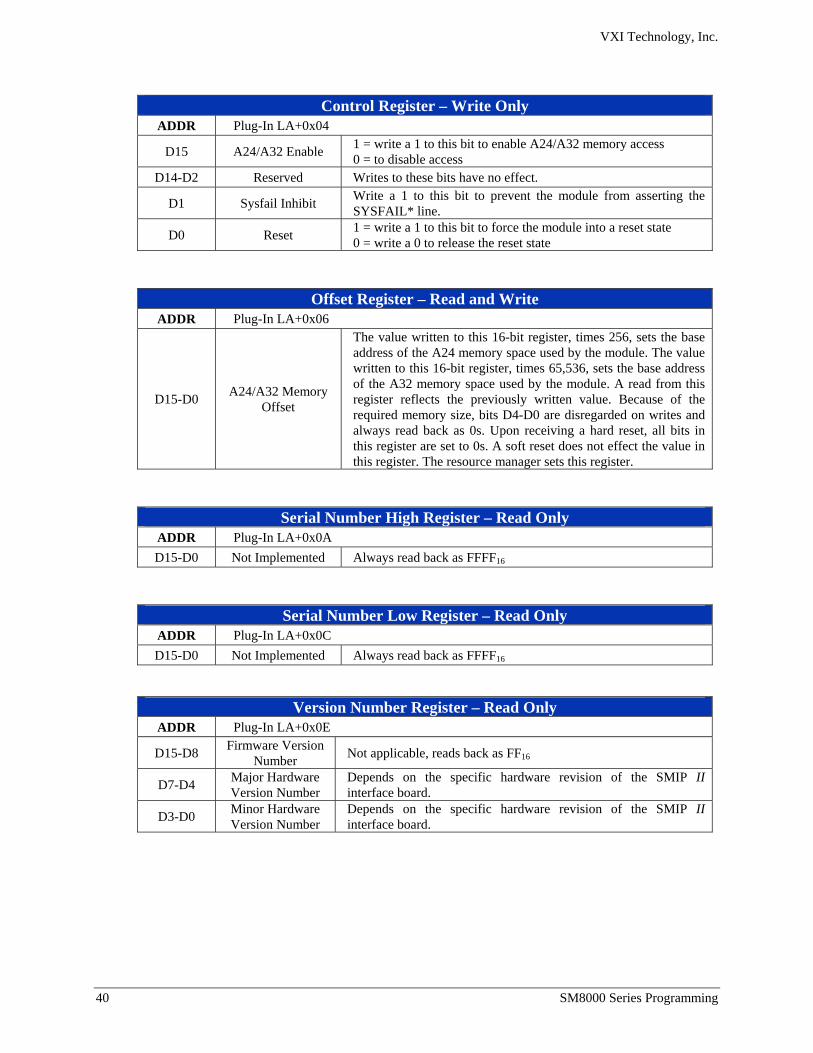
Control Register – Write Only
ADDR Plug-In LA+0x04
D15 A24/A32 Enable 1 = write a 1 to this bit to enable A24/A32 memory access 0 = to disable access
D14-D2 Reserved Writes to these bits have no effect.
D1 Sysfail Inhibit Write a 1 to this bit to prevent the module from asserting the SYSFAIL* line.
D0 Reset 1 = write a 1 to this bit to force the module into a reset state 0 = write a 0 to release the reset state
Offset Register – Read and Write ADDR Plug-In LA+0x06
D15-D0 A24/A32 Memory Offset
The value written to this 16-bit register, times 256, sets the base address of the A24 memory space used by the module. The value written to this 16-bit register, times 65,536, sets the base address of the A32 memory space used by the module. A read from this register reflects the previously written value. Because of the required memory size, bits D4-D0 are disregarded on writes and always read back as 0s. Upon receiving a hard reset, all bits in this register are set to 0s. A soft reset does not effect the value in this register. The resource manager sets this register.
Serial Number High Register – Read Only ADDR Plug-In LA+0x0A D15-D0 Not Implemented Always read back as FFFF16
Serial Number Low Register – Read Only ADDR Plug-In LA+0x0C D15-D0 Not Implemented Always read back as FFFF16
Version Number Register – Read Only ADDR Plug-In LA+0x0E
D15-D8 Firmware Version Number Not applicable, reads back as FF16
D7-D4 Major Hardware Version Number
Depends on the specific hardware revision of the SMIP II interface board.
D3-D0 Minor Hardware Version Number
Depends on the specific hardware revision of the SMIP II interface board.
VXI Technology, Inc.
SM8000 Series Programming 41
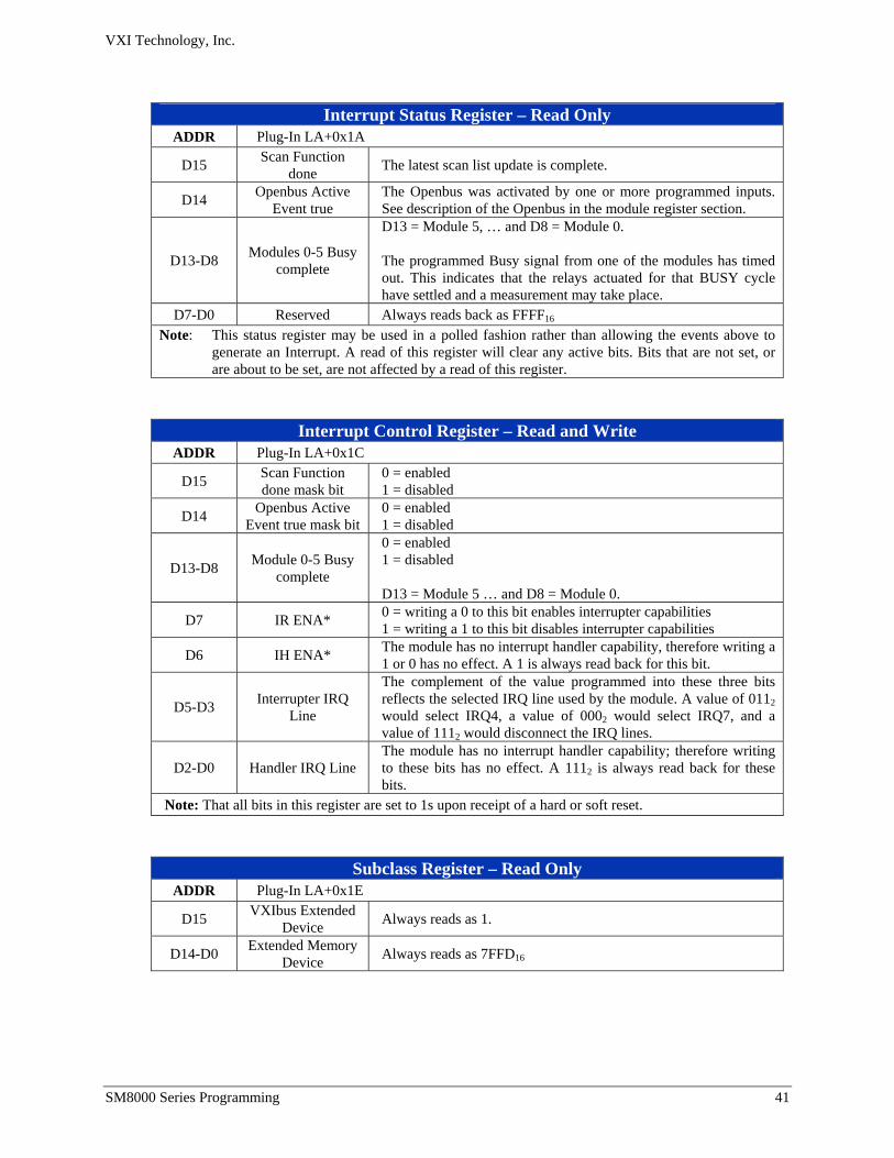
Interrupt Status Register – Read Only
ADDR Plug-In LA+0x1A
D15 Scan Function done The latest scan list update is complete.
D14 Openbus Active Event true
The Openbus was activated by one or more programmed inputs. See description of the Openbus in the module register section.
D13-D8 Modules 0-5 Busy complete
D13 = Module 5, … and D8 = Module 0. The programmed Busy signal from one of the modules has timed out. This indicates that the relays actuated for that BUSY cycle have settled and a measurement may take place.
D7-D0 Reserved Always reads back as FFFF16
Note: This status register may be used in a polled fashion rather than allowing the events above to generate an Interrupt. A read of this register will clear any active bits. Bits that are not set, or are about to be set, are not affected by a read of this register.
Interrupt Control Register – Read and Write ADDR Plug-In LA+0x1C
D15 Scan Function done mask bit
0 = enabled 1 = disabled
D14 Openbus Active Event true mask bit
0 = enabled 1 = disabled
D13-D8 Module 0-5 Busy complete
0 = enabled 1 = disabled D13 = Module 5 … and D8 = Module 0.
D7 IR ENA* 0 = writing a 0 to this bit enables interrupter capabilities 1 = writing a 1 to this bit disables interrupter capabilities
D6 IH ENA* The module has no interrupt handler capability, therefore writing a 1 or 0 has no effect. A 1 is always read back for this bit.
D5-D3 Interrupter IRQ Line
The complement of the value programmed into these three bits reflects the selected IRQ line used by the module. A value of 0112 would select IRQ4, a value of 0002 would select IRQ7, and a value of 1112 would disconnect the IRQ lines.
D2-D0 Handler IRQ Line The module has no interrupt handler capability; therefore writing to these bits has no effect. A 1112 is always read back for these bits.
Note: That all bits in this register are set to 1s upon receipt of a hard or soft reset.
Subclass Register – Read Only ADDR Plug-In LA+0x1E
D15 VXIbus Extended Device Always reads as 1.
D14-D0 Extended Memory Device Always reads as 7FFD16
VXI Technology, Inc.
42 SM8000 Series Programming
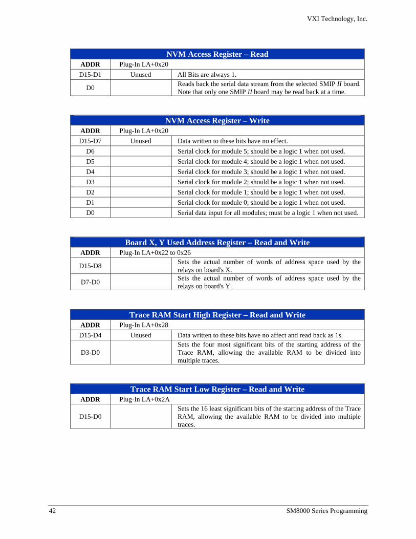
NVM Access Register – Read
ADDR Plug-In LA+0x20 D15-D1 Unused All Bits are always 1.
D0 Reads back the serial data stream from the selected SMIP II board. Note that only one SMIP II board may be read back at a time.
NVM Access Register – Write ADDR Plug-In LA+0x20 D15-D7 Unused Data written to these bits have no effect.
D6 Serial clock for module 5; should be a logic 1 when not used. D5 Serial clock for module 4; should be a logic 1 when not used. D4 Serial clock for module 3; should be a logic 1 when not used. D3 Serial clock for module 2; should be a logic 1 when not used. D2 Serial clock for module 1; should be a logic 1 when not used. D1 Serial clock for module 0; should be a logic 1 when not used. D0 Serial data input for all modules; must be a logic 1 when not used.
Board X, Y Used Address Register – Read and Write ADDR Plug-In LA+0x22 to 0x26
D15-D8 Sets the actual number of words of address space used by the relays on board's X.
D7-D0 Sets the actual number of words of address space used by the relays on board's Y.
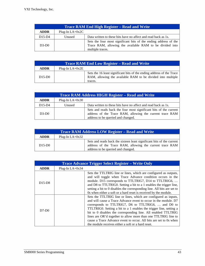
Trace RAM Start High Register – Read and Write ADDR Plug-In LA+0x28 D15-D4 Unused Data written to these bits have no affect and read back as 1s.
D3-D0 Sets the four most significant bits of the starting address of the Trace RAM, allowing the available RAM to be divided into multiple traces.
Trace RAM Start Low Register – Read and Write ADDR Plug-In LA+0x2A
D15-D0 Sets the 16 least significant bits of the starting address of the Trace RAM, allowing the available RAM to be divided into multiple traces.
VXI Technology, Inc.
SM8000 Series Programming 43
Trace RAM End High Register – Read and Write
ADDR Plug-In LA+0x2C D15-D4 Unused Data written to these bits have no affect and read back as 1s.
D3-D0 Sets the four most significant bits of the ending address of the Trace RAM, allowing the available RAM to be divided into multiple traces.
Trace RAM End Low Register – Read and Write ADDR Plug-In LA+0x2E
D15-D0 Sets the 16 least significant bits of the ending address of the Trace RAM, allowing the available RAM to be divided into multiple traces.
Trace RAM Address HIGH Register – Read and Write ADDR Plug-In LA+0x30 D15-D4 Unused Data written to these bits have no affect and read back as 1s.
D3-D0 Sets and reads back the four most significant bits of the current address of the Trace RAM, allowing the current trace RAM address to be queried and changed.
Trace RAM Address LOW Register – Read and Write ADDR Plug-In LA+0x32
D15-D0 Sets and reads back the sixteen least significant bits of the current address of the Trace RAM, allowing the current trace RAM address to be queried and changed.
Trace Advance Trigger Select Register – Write Only ADDR Plug-In LA+0x34
D15-D8
Sets the TTLTRIG line or lines, which are configured as outputs, and will toggle when Trace Advance condition occurs in the module. D15 corresponds to TTLTRIG7, D14 to TTLTRIG6, … and D8 to TTLTRIG0. Setting a bit to a 1 enables the trigger line, setting a bit to 0 disables the corresponding line. All bits are set to 0s when either a soft or a hard reset is received by the module.
D7-D0
Sets the TTLTRIG line or lines, which are configured as inputs, and will cause a Trace Advance event to occur in the module. D7 corresponds to TTLTRIG7, D6 to TTLTRIG6, … and D0 to TTLTRIG0. Setting a bit to a 1 enables the trigger line, setting a bit to 0 disables the corresponding line. All enabled TTLTRIG lines are OR’d together to allow more than one TTLTRIG line to cause a Trace Advance event to occur. All bits are set to 0s when the module receives either a soft or a hard reset.
VXI Technology, Inc.
44 SM8000 Series Programming
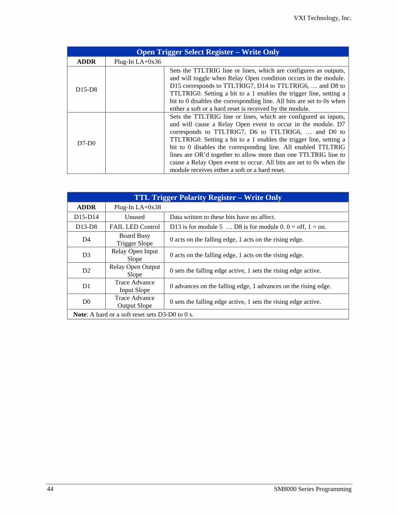
Open Trigger Select Register – Write Only
ADDR Plug-In LA+0x36
D15-D8
Sets the TTLTRIG line or lines, which are configures as outputs, and will toggle when Relay Open condition occurs in the module. D15 corresponds to TTLTRIG7, D14 to TTLTRIG6, … and D8 to TTLTRIG0. Setting a bit to a 1 enables the trigger line, setting a bit to 0 disables the corresponding line. All bits are set to 0s when either a soft or a hard reset is received by the module.
D7-D0
Sets the TTLTRIG line or lines, which are configured as inputs, and will cause a Relay Open event to occur in the module. D7 corresponds to TTLTRIG7, D6 to TTLTRIG6, … and D0 to TTLTRIG0. Setting a bit to a 1 enables the trigger line, setting a bit to 0 disables the corresponding line. All enabled TTLTRIG lines are OR’d together to allow more than one TTLTRIG line to cause a Relay Open event to occur. All bits are set to 0s when the module receives either a soft or a hard reset.
TTL Trigger Polarity Register – Write Only ADDR Plug-In LA+0x38
D15-D14 Unused Data written to these bits have no affect. D13-D8 FAIL LED Control D13 is for module 5 … D8 is for module 0. 0 = off, 1 = on.
D4 Board Busy Trigger Slope 0 acts on the falling edge, 1 acts on the rising edge.
D3 Relay Open Input Slope 0 acts on the falling edge, 1 acts on the rising edge.
D2 Relay Open Output Slope 0 sets the falling edge active, 1 sets the rising edge active.
D1 Trace Advance Input Slope 0 advances on the falling edge, 1 advances on the rising edge.
D0 Trace Advance Output Slope 0 sets the falling edge active, 1 sets the rising edge active.
Note: A hard or a soft reset sets D3-D0 to 0 s.
VXI Technology, Inc.
SM8000 Series Programming 45
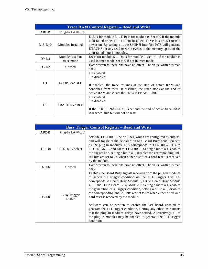
Trace RAM Control Register – Read and Write
ADDR Plug-In LA+0x3A
D15-D10 Modules Installed
D15 is for module 5 ... D10 is for module 0. Set to 0 if the module is installed or set to a 1 if not installed. These bits are set to 0 at power on. By setting a 1, the SMIP II Interface PCB will generate DTACK* for any read or write cycles to the memory space of the uninstalled plug-in modules.
D9-D4 Modules used in trace mode
D9 is for module 5 ... D4 is for module 0. Set to 1 if the module is used in trace mode, set to 0 if not in trace mode.
D3-D2 Unused Data written to these bits have no effect. The value written is read back.
D1 LOOP ENABLE
1 = enabled 0 = disabled If enabled, the trace resumes at the start of active RAM and continues from there. If disabled, the trace stops at the end of active RAM and clears the TRACE ENABLE bit.
D0 TRACE ENABLE
1 = enabled 0 = disabled If the LOOP ENABLE bit is set and the end of active trace RAM is reached, this bit will not be reset.
Busy Trigger Control Register – Read and Write ADDR Plug-In LA+0x3C
D15-D8 TTLTRIG Select
Sets the TTLTRIG Line or Lines, which are configured as outputs, and will toggle at the de-assertion of a Board Busy condition sent by the plug-in modules. D15 corresponds to TTLTRIG7, D14 to TTLTRIG6, … and D8 to TTLTRIG0. Setting a bit to a 1, enables the trigger line, setting a bit to a 0, disables the corresponding line. All bits are set to 0's when either a soft or a hard reset is received by the module.
D7-D6 Unused Data written to these bits have no effect. The value written is read back.
D5-D0 Busy Trigger Enable
Enables the Board Busy signals received from the plug-in modules to generate a trigger condition on the TTL Trigger Bus. D5 corresponds to Board Busy Module 5, D4 to Board Busy Module 4, … and D0 to Board Busy Module 0. Setting a bit to a 1, enables the generation of a Trigger condition, setting a bit to a 0, disables the corresponding line. All bits are set to 0's when either a soft or a hard reset is received by the module. Software can be written to enable the last board updated to generate the TTLTrigger condition, alerting any other instruments that the plug0in modules' relays have settled. Alternatively, all of the plug-in modules may be enabled to generate the TTLTrigger condition.
VXI Technology, Inc.
46 SM8000 Series Programming
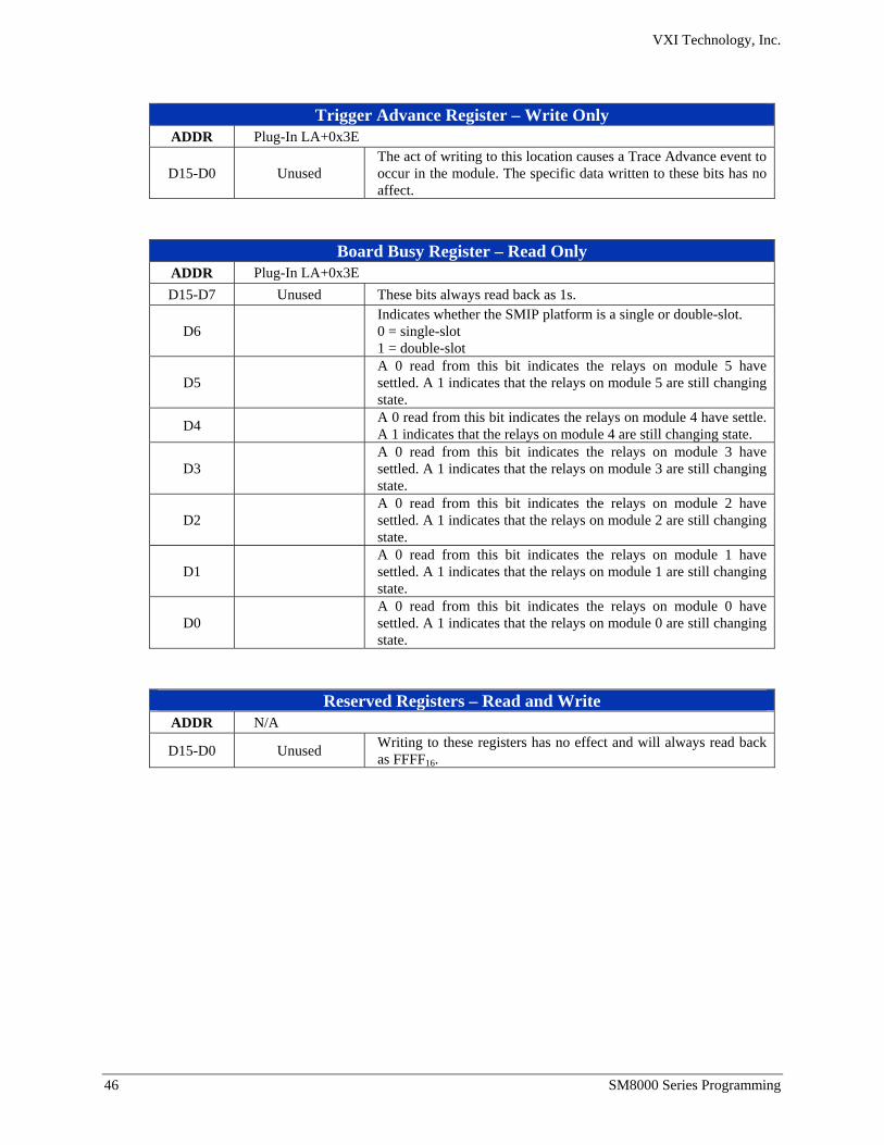
Trigger Advance Register – Write Only
ADDR Plug-In LA+0x3E
D15-D0 Unused The act of writing to this location causes a Trace Advance event to occur in the module. The specific data written to these bits has no affect.
Board Busy Register – Read Only ADDR Plug-In LA+0x3E D15-D7 Unused These bits always read back as 1s.
D6 Indicates whether the SMIP platform is a single or double-slot. 0 = single-slot 1 = double-slot
D5 A 0 read from this bit indicates the relays on module 5 have settled. A 1 indicates that the relays on module 5 are still changing state.
D4 A 0 read from this bit indicates the relays on module 4 have settle. A 1 indicates that the relays on module 4 are still changing state.
D3 A 0 read from this bit indicates the relays on module 3 have settled. A 1 indicates that the relays on module 3 are still changing state.
D2 A 0 read from this bit indicates the relays on module 2 have settled. A 1 indicates that the relays on module 2 are still changing state.
D1 A 0 read from this bit indicates the relays on module 1 have settled. A 1 indicates that the relays on module 1 are still changing state.
D0 A 0 read from this bit indicates the relays on module 0 have settled. A 1 indicates that the relays on module 0 are still changing state.
Reserved Registers – Read and Write ADDR N/A
D15-D0 Unused Writing to these registers has no effect and will always read back as FFFF16.
VXI Technology, Inc.
SM8000 Series Programming 47
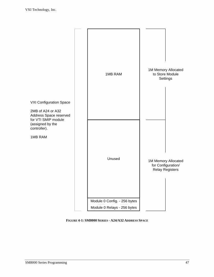
Module 0 Config. - 256 bytes
Module 0 Relays - 256 bytes
VXI Configuration Space
2MB of A24 or A32Address Space reservedfor VTI SMIP module(assigned by thecontroller).
1MB RAM
1M Memory Allocatedto Store Module
Settings1MB RAM
1M Memory Allocatedfor Configuration/Relay Registers
Unused
FIGURE 4-1: SM8000 SERIES - A24/A32 ADDRESS SPACE
VXI Technology, Inc.
48 SM8000 Series Programming
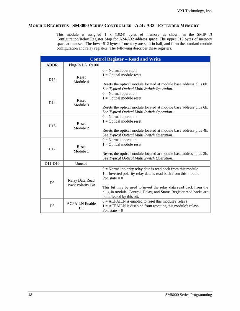
MODULE REGISTERS - SM8000 SERIES CONTROLLER - A24 / A32 - EXTENDED MEMORY
This module is assigned 1 k (1024) bytes of memory as shown in the SMIP II Configuration/Relay Register Map for A24/A32 address space. The upper 512 bytes of memory space are unused. The lower 512 bytes of memory are split in half, and form the standard module configuration and relay registers. The following describes these registers.
Control Register – Read and Write
ADDR Plug-In LA+0x100
D15 Reset Module 4
0 = Normal operation 1 = Optical module reset Resets the optical module located at module base address plus 8h. See Typical Optical Multi Switch Operation.
D14 Reset Module 3
0 = Normal operation 1 = Optical module reset Resets the optical module located at module base address plus 6h. See Typical Optical Multi Switch Operation.
D13 Reset Module 2
0 = Normal operation 1 = Optical module reset Resets the optical module located at module base address plus 4h. See Typical Optical Multi Switch Operation.
D12 Reset Module 1
0 = Normal operation 1 = Optical module reset Resets the optical module located at module base address plus 2h. See Typical Optical Multi Switch Operation.
D11-D10 Unused
D9 Relay Data Read Back Polarity Bit
0 = Normal polarity relay data is read back from this module 1 = Inverted polarity relay data is read back from this module Pon state = 0 This bit may be used to invert the relay data read back from the plug-in module. Control, Delay, and Status Register read backs are not effected by this bit.
D8 ACFAILN Enable Bit
0 = ACFAILN is enabled to reset this module's relays 1 = ACFAILN is disabled from resetting this module's relays Pon state = 0
VXI Technology, Inc.
SM8000 Series Programming 49
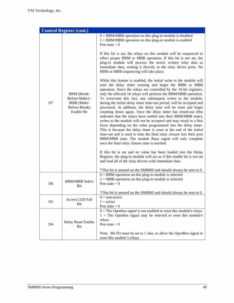
Control Register (cont.)
D7
BBM (Break-Before-Make) / MBB (Make-Before-Break)
Enable Bit
0 = BBM/MBB operation on this plug-in module is disabled 1 = BBM/MBB operation on this plug-in module is enabled Pon state = 0 If this bit is set, the relays on this module will be sequenced to effect proper BBM or MBB operation. If this bit is not set, the plug-in module will process the newly written relay data as immediate data, writing it directly to the relay driver ports. No BBM or MBB sequencing will take place. While this feature is enabled, the initial write to the module will start the delay timer running and begin the BBM or MBB operation. Since the relays are controlled by the 16-bit registers, only the effected 16 relays will perform the BBM/MBB operation. To overcome this fact, any subsequent writes to the module, during the initial delay timer time-out period, will be accepted and processed. In addition, the delay time will be reset and begin counting down again. Once the delay timer has timed-out (this indicates that the relays have settled into their BBM/MBB state), writes to the module will not be accepted and may result in a Bus Error depending on the value programmed into the delay timer. This is because the delay timer is reset at the end of the initial time-out and is used to time the final relay closure into their post BBM/MBB state. The module Busy signal will only complete once the final relay closure state is reached. If this bit is set and no value has been loaded into the Delay Register, the plug-in module will act as if this enable bit is not set and load all of the relay drivers with immediate data. *This bit is unused on the SM8000 and should always be sent to 0.
D6 BBM/MBB Select Bit
0 = BBM operation on this plug-in module is selected 1 = MBB operation on this plug-in module is selected Pon state = 0 *This bit is unused on the SM8000 and should always be sent to 0.
D5 Access LED Fail Bit
0 = non-active 1 = active Pon state = 0
D4 Relay Reset Enable Bit
0 = The Openbus signal is not enabled to reset this module's relays 1 = The Openbus signal may be selected to reset this module's relays Pon state = 0 Note: Bit D3 must be set to 1 also, to allow the OpenBus signal to reset this module’s relays
VXI Technology, Inc.
50 SM8000 Series Programming
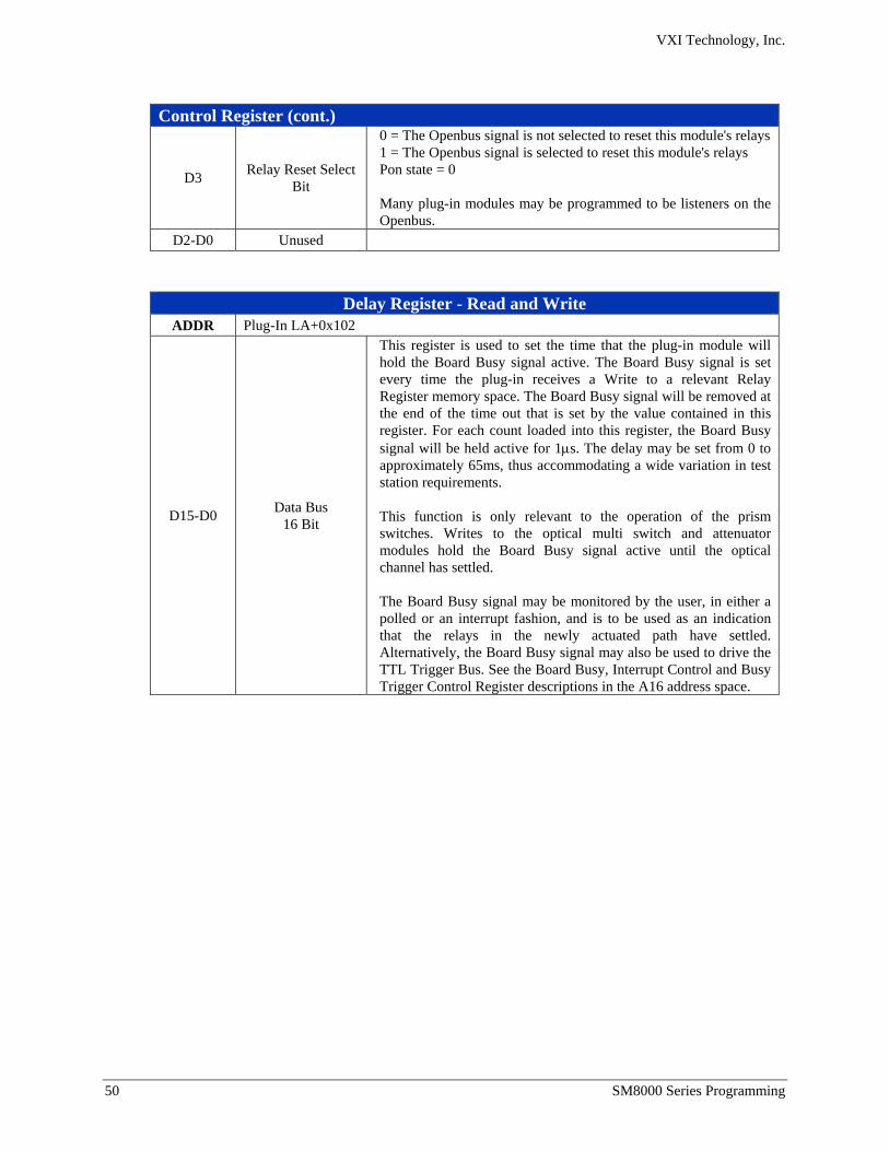
Control Register (cont.)
D3 Relay Reset Select Bit
0 = The Openbus signal is not selected to reset this module's relays 1 = The Openbus signal is selected to reset this module's relays Pon state = 0 Many plug-in modules may be programmed to be listeners on the Openbus.
D2-D0 Unused
Delay Register - Read and Write ADDR Plug-In LA+0x102
D15-D0 Data Bus 16 Bit
This register is used to set the time that the plug-in module will hold the Board Busy signal active. The Board Busy signal is set every time the plug-in receives a Write to a relevant Relay Register memory space. The Board Busy signal will be removed at the end of the time out that is set by the value contained in this register. For each count loaded into this register, the Board Busy signal will be held active for 1μs. The delay may be set from 0 to approximately 65ms, thus accommodating a wide variation in test station requirements. This function is only relevant to the operation of the prism switches. Writes to the optical multi switch and attenuator modules hold the Board Busy signal active until the optical channel has settled. The Board Busy signal may be monitored by the user, in either a polled or an interrupt fashion, and is to be used as an indication that the relays in the newly actuated path have settled. Alternatively, the Board Busy signal may also be used to drive the TTL Trigger Bus. See the Board Busy, Interrupt Control and Busy Trigger Control Register descriptions in the A16 address space.
VXI Technology, Inc.
SM8000 Series Programming 51
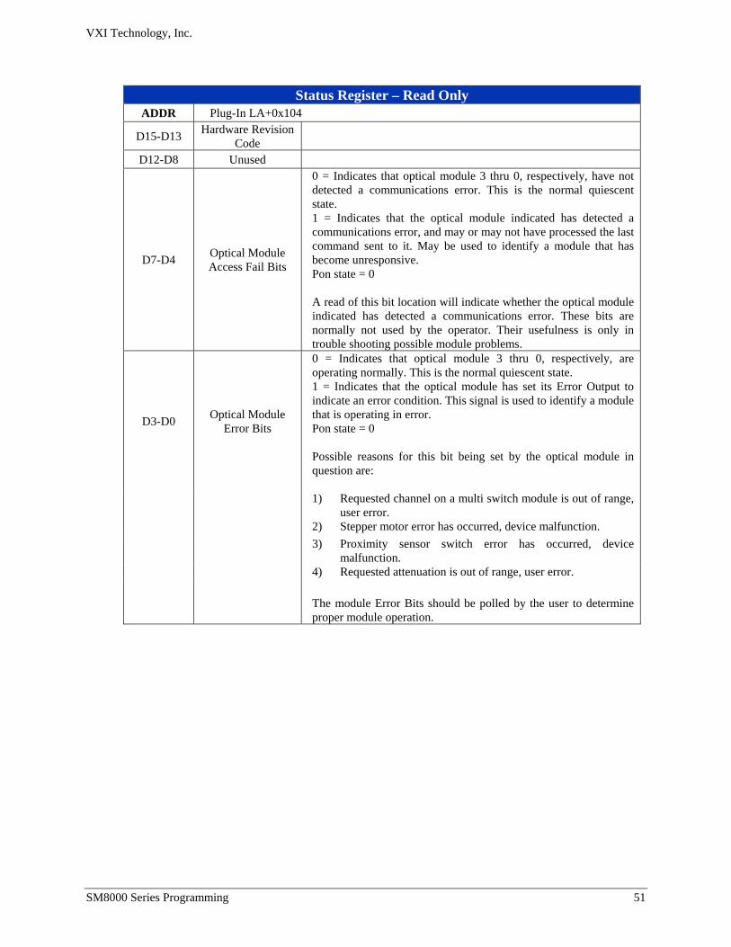
Status Register – Read Only
ADDR Plug-In LA+0x104
D15-D13 Hardware Revision Code
D12-D8 Unused
D7-D4 Optical Module Access Fail Bits
0 = Indicates that optical module 3 thru 0, respectively, have not detected a communications error. This is the normal quiescent state. 1 = Indicates that the optical module indicated has detected a communications error, and may or may not have processed the last command sent to it. May be used to identify a module that has become unresponsive. Pon state = 0 A read of this bit location will indicate whether the optical module indicated has detected a communications error. These bits are normally not used by the operator. Their usefulness is only in trouble shooting possible module problems.
D3-D0 Optical Module Error Bits
0 = Indicates that optical module 3 thru 0, respectively, are operating normally. This is the normal quiescent state. 1 = Indicates that the optical module has set its Error Output to indicate an error condition. This signal is used to identify a module that is operating in error. Pon state = 0 Possible reasons for this bit being set by the optical module in question are:
1) Requested channel on a multi switch module is out of range, user error.
2) Stepper motor error has occurred, device malfunction.
3) Proximity sensor switch error has occurred, device malfunction.
4) Requested attenuation is out of range, user error.
The module Error Bits should be polled by the user to determine proper module operation.
VXI Technology, Inc.
52 SM8000 Series Programming
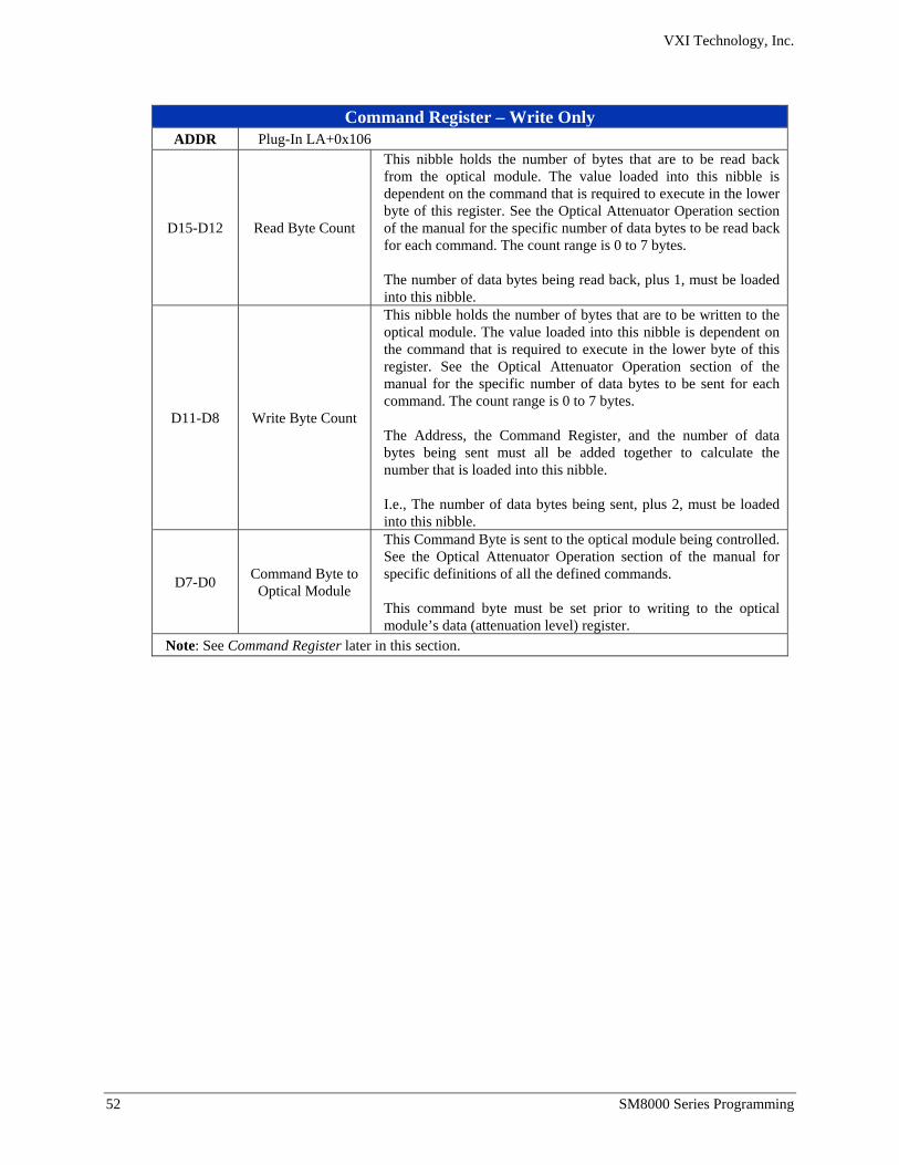
Command Register – Write Only
ADDR Plug-In LA+0x106
D15-D12 Read Byte Count
This nibble holds the number of bytes that are to be read back from the optical module. The value loaded into this nibble is dependent on the command that is required to execute in the lower byte of this register. See the Optical Attenuator Operation section of the manual for the specific number of data bytes to be read back for each command. The count range is 0 to 7 bytes. The number of data bytes being read back, plus 1, must be loaded into this nibble.
D11-D8 Write Byte Count
This nibble holds the number of bytes that are to be written to the optical module. The value loaded into this nibble is dependent on the command that is required to execute in the lower byte of this register. See the Optical Attenuator Operation section of the manual for the specific number of data bytes to be sent for each command. The count range is 0 to 7 bytes. The Address, the Command Register, and the number of data bytes being sent must all be added together to calculate the number that is loaded into this nibble. I.e., The number of data bytes being sent, plus 2, must be loaded into this nibble.
D7-D0 Command Byte to Optical Module
This Command Byte is sent to the optical module being controlled. See the Optical Attenuator Operation section of the manual for specific definitions of all the defined commands. This command byte must be set prior to writing to the optical module’s data (attenuation level) register.
Note: See Command Register later in this section.
VXI Technology, Inc.
SM8000 Series Programming 53
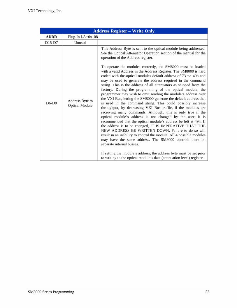
Address Register – Write Only
ADDR Plug-In LA+0x108 D15-D7 Unused
D6-D0 Address Byte to Optical Module
This Address Byte is sent to the optical module being addressed. See the Optical Attenuator Operation section of the manual for the operation of the Address register. To operate the modules correctly, the SM8000 must be loaded with a valid Address in the Address Register. The SM8000 is hard coded with the optical modules default address of 73 => 49h and may be used to generate the address required in the command string. This is the address of all attenuators as shipped from the factory. During the programming of the optical module, the programmer may wish to omit sending the module’s address over the VXI Bus, letting the SM8000 generate the default address that is used in the command string. This could possibly increase throughput, by decreasing VXI Bus traffic, if the modules are receiving many commands. Although, this is only true if the optical module’s address is not changed by the user. It is recommended that the optical module’s address be left at 49h. If the address is to be changed, IT IS IMPERATIVE THAT THE NEW ADDRESS BE WRITTEN DOWN. Failure to do so will result in an inability to control the module. All 4 possible modules may have the same address. The SM8000 controls them on separate internal busses. If setting the module’s address, the address byte must be set prior to writing to the optical module’s data (attenuation level) register.
VXI Technology, Inc.
54 SM8000 Series Programming
DEVICE MEMORY MODULE RELAY CONTROL ADDRESS - SM8000 SERIES OPTICAL SWITCH CONTROLLER
The SM8000 SMIP II plug-in module is assigned 1 k (1024) bytes of memory as shown in the SMIP II Configuration/Relay Register Map for A24/A32 address space as shown below. The lower 512 bytes of each module's memory are used for optical switch and optical module control. The 512 bytes are split in half with the lower 256 bytes used to pass data to the optical modules, and the upper 256 bytes used to hold SM8000 optical module specific control registers. The rest of the upper 1K address space is unused. The base address is as follows:
Module 0 (SM8000) Base Address = 0x0000 The Module Base Address is then added to the A24/A32 Base Address to access a specific module's relays:
Module Relay Address = A24/A32 Base Address + Module Base Address Since only one Model SM8000 may be plugged onto a standard SMIP II carrier, only one module base address, H0000, is used to address the SM8000. This is the case whether or not the SM8000 is housed in a single or double-slot VXI module.
RELAY REGISTER OFFSET
The Relay Register Offset is located within the module's A24/32 address space. When data is sent to the register, the relay register offset is added to the A24/A32 base address and module base address:
Relay Register Address = A24/A32 Base Address + Module Base Address + Register Offset
or
Relay Register Address = Module Relay Address + Register Offset

VXI Technology, Inc.
SM8000 Series Programming 55
WRITING TO THE RELAY REGISTERS
If the SM8000 is used to drive single-mode prism switches, in either latching or non-latching configurations, setting the switches is accomplished through writing to the Relay Register located at Relay Register Offset H0000. Each bit, of this 16-bit register, represents the state of the relay (1 = closed, 0 = open). (Note that bits 15 through 12 are unused.) To change the state of any relay, it is only necessary to write a 16-bit integer to the specified register with the new configuration. For example: • writing a data value of "0" to the register at offset "0" would open the 12 available switches
• writing a data value of 4095 (0x0FFF) to the same register would close the 12 switches
• writing a data value of 4094 (0x0FFE) to the same register would close all switches except
switch number 1
Relay Register 00 – Read and Write ADDR Plug-In LA+0x000
D15-D12 Unused Write has no effect. Read back as 1111.
D11-D0 1x2 or 2x2 Optical
Prism Switch Control Register
0 = Opens optical path. 1 = Closes optical path. Pon state = 0 A read of this bit location will indicate whether the optical path is either closed or open. This register controls the possible 12 prism switches that may be driven by the SM8000.
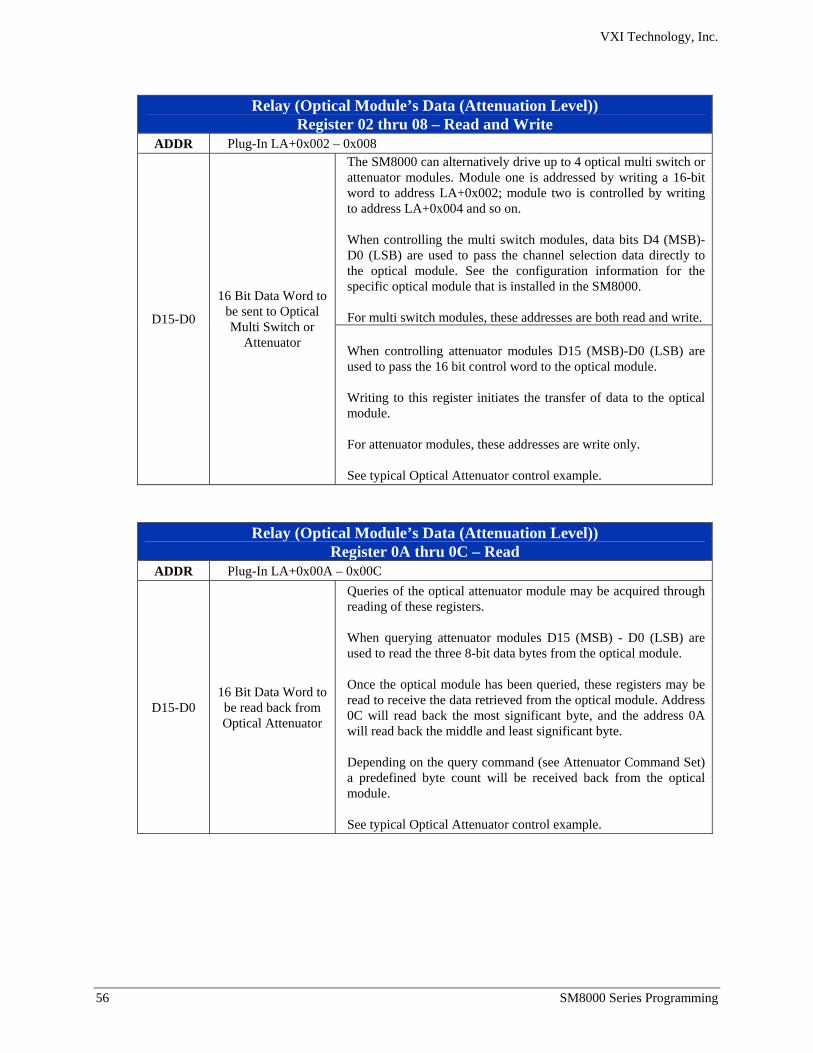
VXI Technology, Inc.
56 SM8000 Series Programming
Relay (Optical Module’s Data (Attenuation Level))
Register 02 thru 08 – Read and Write ADDR Plug-In LA+0x002 – 0x008
The SM8000 can alternatively drive up to 4 optical multi switch or attenuator modules. Module one is addressed by writing a 16-bit word to address LA+0x002; module two is controlled by writing to address LA+0x004 and so on. When controlling the multi switch modules, data bits D4 (MSB)-D0 (LSB) are used to pass the channel selection data directly to the optical module. See the configuration information for the specific optical module that is installed in the SM8000. For multi switch modules, these addresses are both read and write. D15-D0
16 Bit Data Word to be sent to Optical Multi Switch or
Attenuator When controlling attenuator modules D15 (MSB)-D0 (LSB) are used to pass the 16 bit control word to the optical module. Writing to this register initiates the transfer of data to the optical module. For attenuator modules, these addresses are write only. See typical Optical Attenuator control example.
Relay (Optical Module’s Data (Attenuation Level)) Register 0A thru 0C – Read
ADDR Plug-In LA+0x00A – 0x00C
D15-D0 16 Bit Data Word to be read back from Optical Attenuator
Queries of the optical attenuator module may be acquired through reading of these registers. When querying attenuator modules D15 (MSB) - D0 (LSB) are used to read the three 8-bit data bytes from the optical module. Once the optical module has been queried, these registers may be read to receive the data retrieved from the optical module. Address 0C will read back the most significant byte, and the address 0A will read back the middle and least significant byte. Depending on the query command (see Attenuator Command Set) a predefined byte count will be received back from the optical module. See typical Optical Attenuator control example.
VXI Technology, Inc.
SM8000 Series Programming 57
PROGRAMMING EXAMPLES TYPICAL OPTICAL MULTI-SWITCH CONTROL EXAMPLE
The optical multi-switch modules are controlled via a 5-bit parallel port. To select the optical switch, the binary number corresponding to the switch is written to the SM8000 optical switch controller. The multi-switch modules may be located at register locations 02 through 08. The following sequence could be used to select switch number 5, on the multi-switch module located at register location 02: 1. Write a 0004h to location 02h. Calculate the relay register address as shown above in the
Relay Register Offset section, where the module relay address is always 0, and the register offset is 02h. This will select the optical path that is associated with optical multi-switch number 5.
2. Once the switch has settled, a read of location 02h would confirm the value of 0004h. 3. To set the multi switch module to another desired switch setting, simply write the BCD
number corresponding to the switch required to the SM8000. 4. To reset the multi switch to the power-on condition, i.e. no optical paths connected, the
following sequence must be performed: a) Set the optical module’s corresponding Reset Bit in the Control Register to ‘1’. b) Write a x0h to the optical module. c) Set the Reset Bit in the Control Register back to “0”.
VXI Technology, Inc.
58 SM8000 Series Programming
TYPICAL OPTICAL ATTENUATOR CONTROL EXAMPLE
The optical attenuator modules are controlled via an I2C bus interface. The bus protocol requires the transmission of the following: • a Module Address • a Command Byte • the number of bytes to send • the number of bytes to receive • the proper data byte(s) that are to be written to, or received from, the optical module (the
command byte(s)). The following sequence should be used to control the modules: Write 1. Load the Address Register with the module’s address. The default address of the modules as
shipped from the factory is 73 => 49h. (This step may be skipped, see Address Register description.)
2. Load the Command Register with the number of bytes to be received plus 1, the number of
bytes to be sent, and the proper command. 3. Write/Read the appropriate Relay Register 02 through 08 depending on the module being
controlled. Read 1. Load the Address Register with the module’s address. The default address of the modules as
shipped from the factory is 73 => 49h. (This step may be skipped, see Address Register description.)
2. Load the Command Register with the number of bytes to be received plus 1, the number of
bytes to be sent, and the proper command (a query command). 3. Write/Read the appropriate Relay Register 02 through 08 depending on the module being
queried (write a “0”, the data is ignored). 4. Read the appropriate Relay Register 0A through 0C depending on the number of bytes that
are to be received from the module being queried. See Attenuator Command Set.
Note These read back registers are common to all four of the possible attenuator modules that may be installed. A subsequent write to any of the Relay Registers 02 through 08 will corrupt these registers.
VXI Technology, Inc.
SM8000 Series Programming 59
Note To operate the modules correctly, the SM8000 must be loaded with a valid Address in the Address Register. The SM8000 is hard coded at the factory with the optical modules default address of 73 => 49h, and may be used to generate the address used in the command. This is the address of all attenuators as shipped from the factory. During the programming of the optical module, the programmer may wish to omit sending the module’s address over the VXI Bus, letting the SM8000 generate the default address that is used in the command string. This could possibly increase throughput, by decreasing VXI Bus traffic, if the modules are receiving many commands, although this is only true if the optical module’s address is not changed by the user. If the address is to be changed, IT IS IMPERATIVE THAT THE NEW ADDRESS BE WRITTEN DOWN. Failure to do so will result in an inability to control the module. All four possible modules may have the same address. The SM8000 controls them on separate internal busses. VTI STRONGLY RECOMMENDS THAT THE OPTICAL MODULE’S ADDRESS BE LEFT AT 49h.
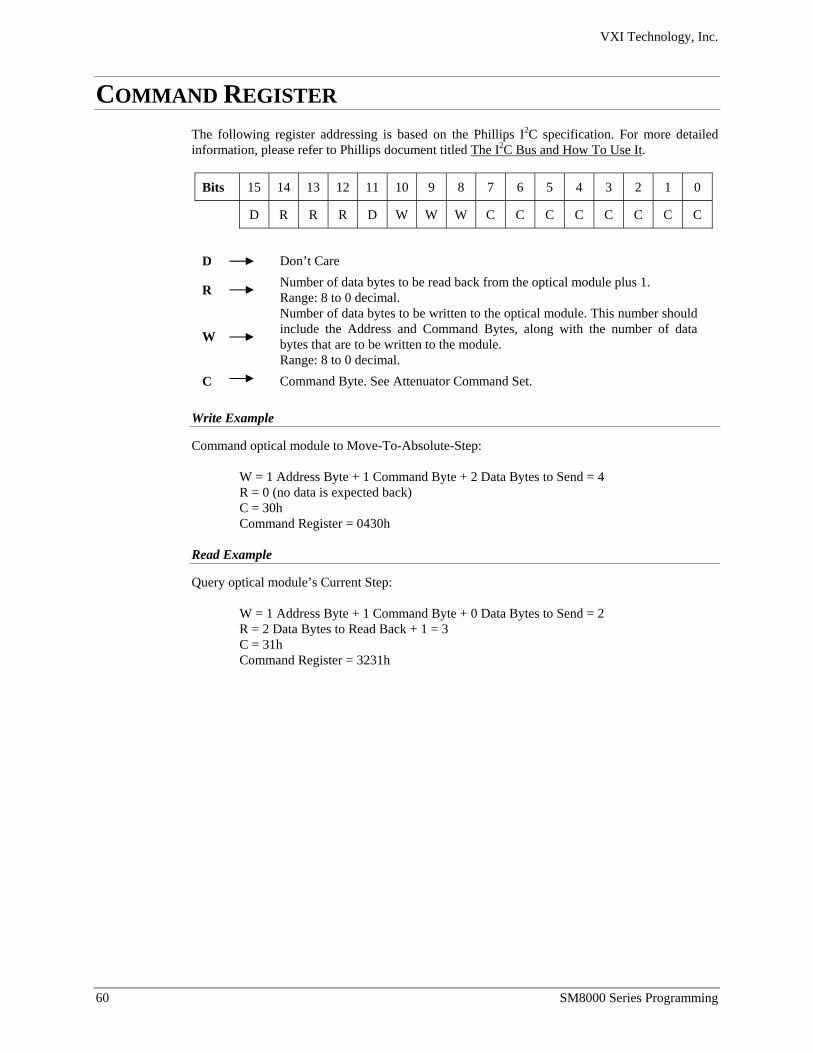
VXI Technology, Inc.
60 SM8000 Series Programming
COMMAND REGISTER The following register addressing is based on the Phillips I2C specification. For more detailed information, please refer to Phillips document titled The I2C Bus and How To Use It.
Bits 15 14 13 12 11 10 9 8 7 6 5 4 3 2 1 0
D R R R D W W W C C C C C C C C
D Don’t Care
R Number of data bytes to be read back from the optical module plus 1. Range: 8 to 0 decimal.
W
Number of data bytes to be written to the optical module. This number should include the Address and Command Bytes, along with the number of data bytes that are to be written to the module. Range: 8 to 0 decimal.
C Command Byte. See Attenuator Command Set. Write Example
Command optical module to Move-To-Absolute-Step:
W = 1 Address Byte + 1 Command Byte + 2 Data Bytes to Send = 4 R = 0 (no data is expected back) C = 30h Command Register = 0430h
Read Example
Query optical module’s Current Step:
W = 1 Address Byte + 1 Command Byte + 0 Data Bytes to Send = 2 R = 2 Data Bytes to Read Back + 1 = 3 C = 31h Command Register = 3231h
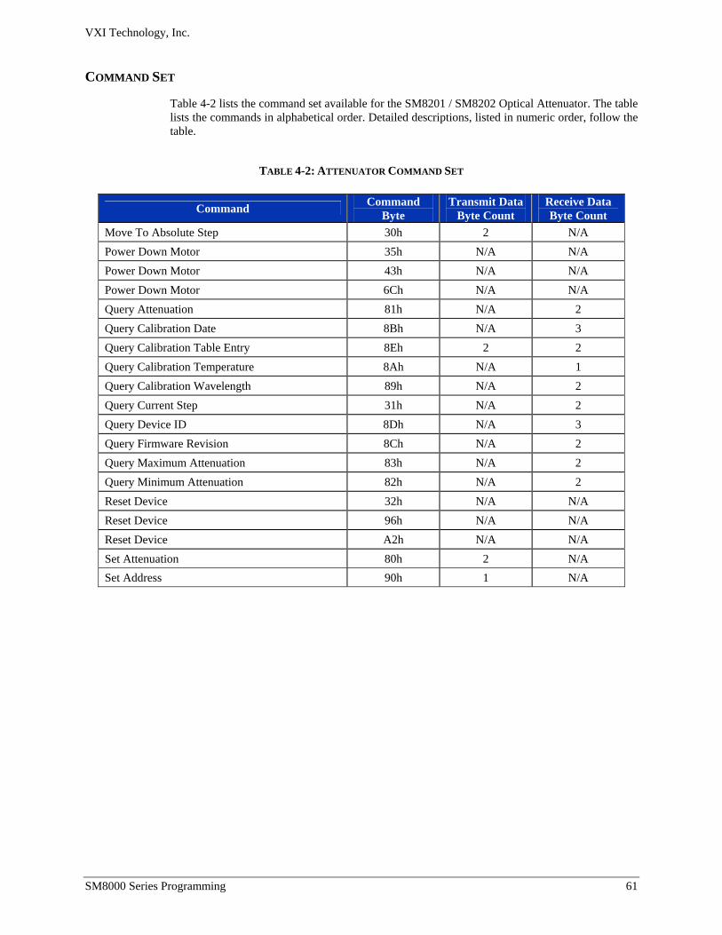
VXI Technology, Inc.
SM8000 Series Programming 61
COMMAND SET
Table 4-2 lists the command set available for the SM8201 / SM8202 Optical Attenuator. The table lists the commands in alphabetical order. Detailed descriptions, listed in numeric order, follow the table.
TABLE 4-2: ATTENUATOR COMMAND SET
Command Command Byte
Transmit Data Byte Count
Receive Data Byte Count
Move To Absolute Step 30h 2 N/A Power Down Motor 35h N/A N/A Power Down Motor 43h N/A N/A Power Down Motor 6Ch N/A N/A Query Attenuation 81h N/A 2 Query Calibration Date 8Bh N/A 3 Query Calibration Table Entry 8Eh 2 2 Query Calibration Temperature 8Ah N/A 1 Query Calibration Wavelength 89h N/A 2 Query Current Step 31h N/A 2 Query Device ID 8Dh N/A 3 Query Firmware Revision 8Ch N/A 2 Query Maximum Attenuation 83h N/A 2 Query Minimum Attenuation 82h N/A 2 Reset Device 32h N/A N/A Reset Device 96h N/A N/A Reset Device A2h N/A N/A Set Attenuation 80h 2 N/A Set Address 90h 1 N/A
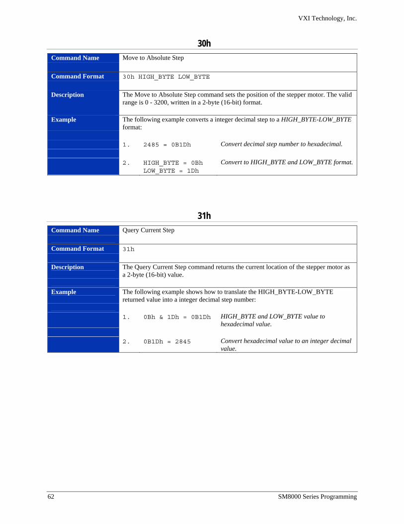
VXI Technology, Inc.
62 SM8000 Series Programming
30h Command Name Move to Absolute Step Command Format 30h HIGH_BYTE LOW_BYTE
Description The Move to Absolute Step command sets the position of the stepper motor. The valid
range is 0 - 3200, written in a 2-byte (16-bit) format. Example The following example converts a integer decimal step to a HIGH_BYTE-LOW_BYTE
format: 1. 2485 = 0B1Dh Convert decimal step number to hexadecimal. 2. HIGH_BYTE = 0Bh
LOW_BYTE = 1Dh Convert to HIGH_BYTE and LOW_BYTE format.
31h Command Name Query Current Step Command Format 31h
Description The Query Current Step command returns the current location of the stepper motor as
a 2-byte (16-bit) value. Example The following example shows how to translate the HIGH_BYTE-LOW_BYTE
returned value into a integer decimal step number: 1. 0Bh & 1Dh = 0B1Dh HIGH_BYTE and LOW_BYTE value to
hexadecimal value. 2. 0B1Dh = 2845 Convert hexadecimal value to an integer decimal
value.
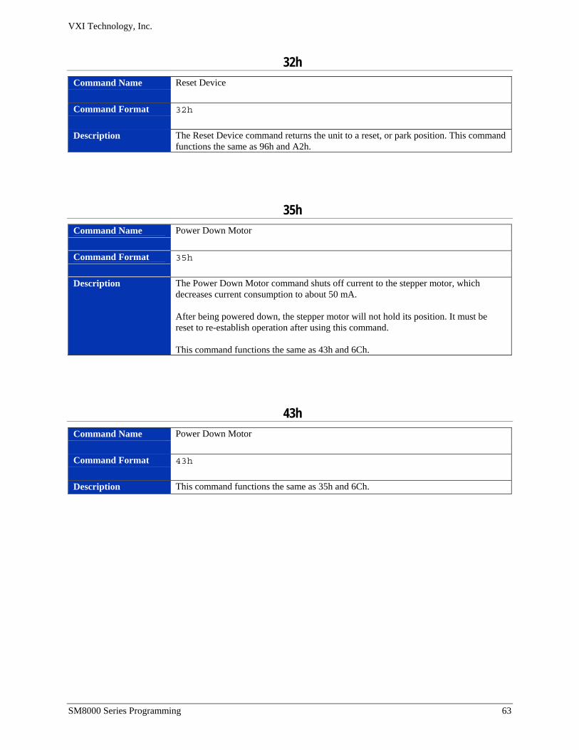
VXI Technology, Inc.
SM8000 Series Programming 63
32h Command Name Reset Device Command Format 32h
Description The Reset Device command returns the unit to a reset, or park position. This command
functions the same as 96h and A2h.
35h Command Name Power Down Motor Command Format 35h
Description The Power Down Motor command shuts off current to the stepper motor, which
decreases current consumption to about 50 mA. After being powered down, the stepper motor will not hold its position. It must be reset to re-establish operation after using this command. This command functions the same as 43h and 6Ch.
43h Command Name Power Down Motor Command Format 43h
Description This command functions the same as 35h and 6Ch.
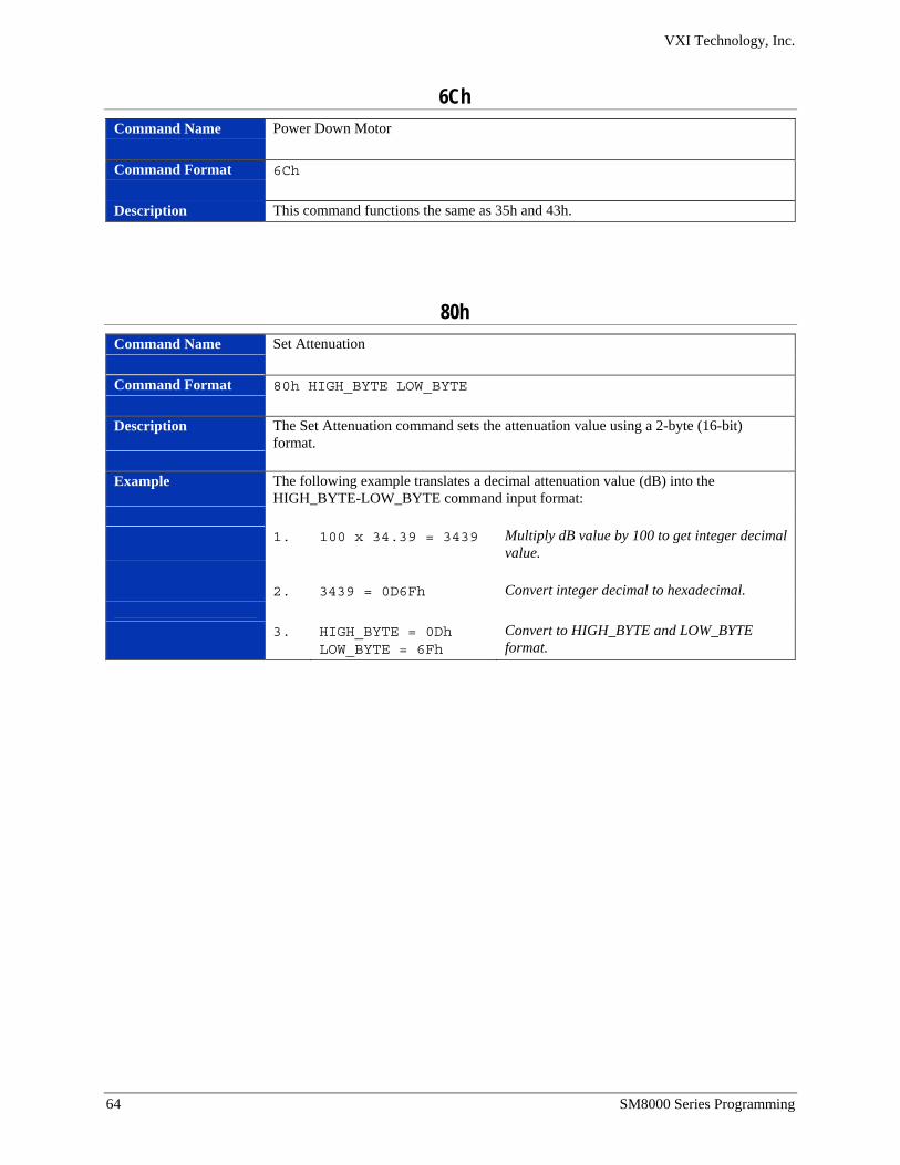
VXI Technology, Inc.
64 SM8000 Series Programming
6Ch Command Name Power Down Motor Command Format 6Ch
Description This command functions the same as 35h and 43h.
80h Command Name Set Attenuation Command Format 80h HIGH_BYTE LOW_BYTE
Description The Set Attenuation command sets the attenuation value using a 2-byte (16-bit)
format. Example The following example translates a decimal attenuation value (dB) into the
HIGH_BYTE-LOW_BYTE command input format: 1. 100 x 34.39 = 3439 Multiply dB value by 100 to get integer decimal
value. 2. 3439 = 0D6Fh Convert integer decimal to hexadecimal. 3. HIGH_BYTE = 0Dh
LOW_BYTE = 6Fh Convert to HIGH_BYTE and LOW_BYTE format.
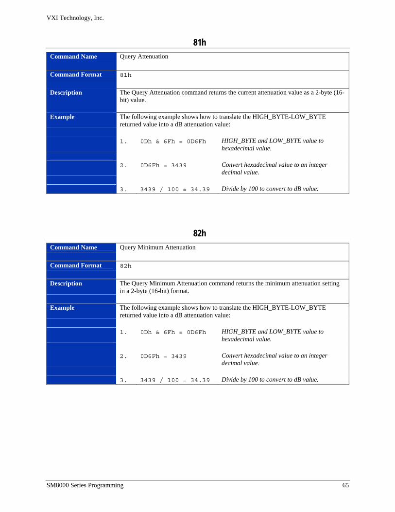
VXI Technology, Inc.
SM8000 Series Programming 65
81h Command Name Query Attenuation Command Format 81h
Description The Query Attenuation command returns the current attenuation value as a 2-byte (16-
bit) value. Example The following example shows how to translate the HIGH_BYTE-LOW_BYTE
returned value into a dB attenuation value: 1. 0Dh & 6Fh = 0D6Fh HIGH_BYTE and LOW_BYTE value to
hexadecimal value. 2. 0D6Fh = 3439 Convert hexadecimal value to an integer
decimal value. 3. 3439 / 100 = 34.39 Divide by 100 to convert to dB value.
82h Command Name Query Minimum Attenuation Command Format 82h
Description The Query Minimum Attenuation command returns the minimum attenuation setting
in a 2-byte (16-bit) format. Example The following example shows how to translate the HIGH_BYTE-LOW_BYTE
returned value into a dB attenuation value: 1. 0Dh & 6Fh = 0D6Fh HIGH_BYTE and LOW_BYTE value to
hexadecimal value. 2. 0D6Fh = 3439 Convert hexadecimal value to an integer
decimal value. 3. 3439 / 100 = 34.39 Divide by 100 to convert to dB value.
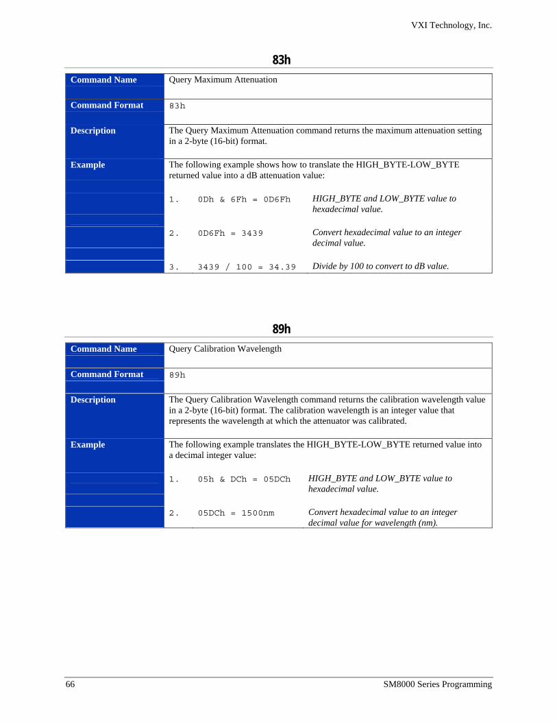
VXI Technology, Inc.
66 SM8000 Series Programming
83h Command Name Query Maximum Attenuation Command Format 83h
Description The Query Maximum Attenuation command returns the maximum attenuation setting
in a 2-byte (16-bit) format. Example The following example shows how to translate the HIGH_BYTE-LOW_BYTE
returned value into a dB attenuation value: 1. 0Dh & 6Fh = 0D6Fh HIGH_BYTE and LOW_BYTE value to
hexadecimal value. 2. 0D6Fh = 3439 Convert hexadecimal value to an integer
decimal value. 3. 3439 / 100 = 34.39 Divide by 100 to convert to dB value.
89h Command Name Query Calibration Wavelength Command Format 89h
Description The Query Calibration Wavelength command returns the calibration wavelength value
in a 2-byte (16-bit) format. The calibration wavelength is an integer value that represents the wavelength at which the attenuator was calibrated.
Example The following example translates the HIGH_BYTE-LOW_BYTE returned value into
a decimal integer value: 1. 05h & DCh = 05DCh HIGH_BYTE and LOW_BYTE value to
hexadecimal value. 2. 05DCh = 1500nm Convert hexadecimal value to an integer
decimal value for wavelength (nm).
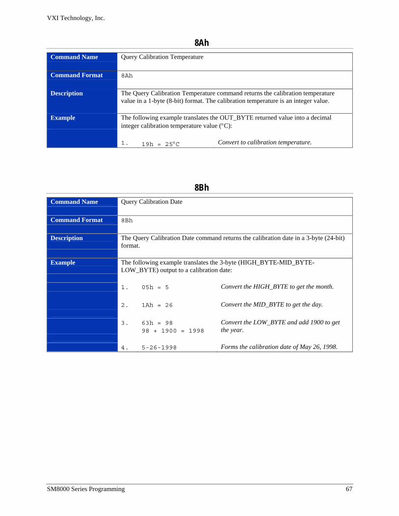
VXI Technology, Inc.
SM8000 Series Programming 67
8Ah Command Name Query Calibration Temperature Command Format 8Ah
Description The Query Calibration Temperature command returns the calibration temperature
value in a 1-byte (8-bit) format. The calibration temperature is an integer value. Example The following example translates the OUT_BYTE returned value into a decimal
integer calibration temperature value (°C): 1. 19h = 25°C Convert to calibration temperature.
8Bh Command Name Query Calibration Date Command Format 8Bh
Description The Query Calibration Date command returns the calibration date in a 3-byte (24-bit)
format. Example The following example translates the 3-byte (HIGH_BYTE-MID_BYTE-
LOW_BYTE) output to a calibration date: 1. 05h = 5 Convert the HIGH_BYTE to get the month. 2. 1Ah = 26 Convert the MID_BYTE to get the day. 3. 63h = 98
98 + 1900 = 1998 Convert the LOW_BYTE and add 1900 to get the year.
4. 5-26-1998 Forms the calibration date of May 26, 1998.
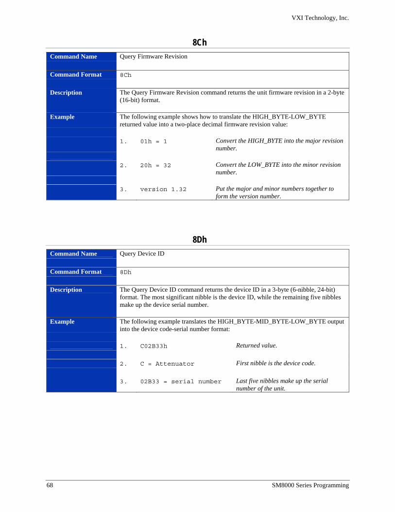
VXI Technology, Inc.
68 SM8000 Series Programming
8Ch Command Name Query Firmware Revision Command Format 8Ch
Description The Query Firmware Revision command returns the unit firmware revision in a 2-byte
(16-bit) format. Example The following example shows how to translate the HIGH_BYTE-LOW_BYTE
returned value into a two-place decimal firmware revision value: 1. 01h = 1 Convert the HIGH_BYTE into the major revision
number. 2. 20h = 32 Convert the LOW_BYTE into the minor revision
number. 3. version 1.32 Put the major and minor numbers together to
form the version number.
8Dh Command Name Query Device ID Command Format 8Dh
Description The Query Device ID command returns the device ID in a 3-byte (6-nibble, 24-bit)
format. The most significant nibble is the device ID, while the remaining five nibbles make up the device serial number.
Example The following example translates the HIGH_BYTE-MID_BYTE-LOW_BYTE output
into the device code-serial number format: 1. C02B33h Returned value. 2. C = Attenuator First nibble is the device code. 3. 02B33 = serial number Last five nibbles make up the serial
number of the unit.
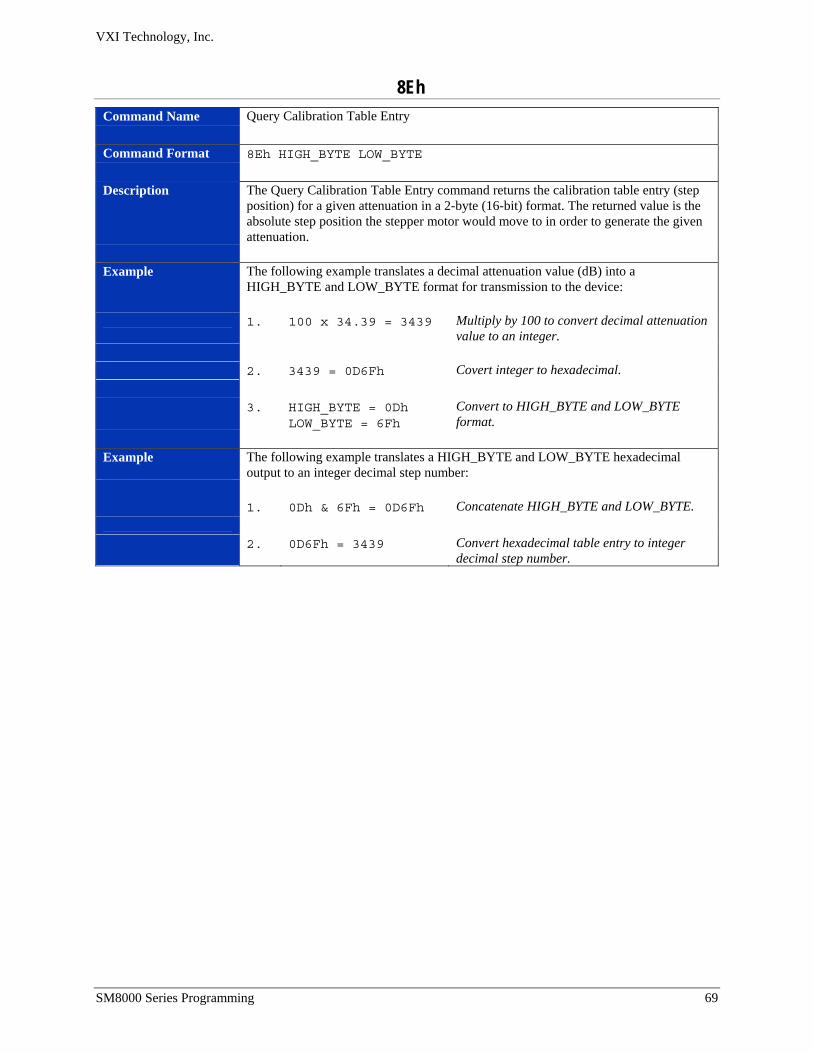
VXI Technology, Inc.
SM8000 Series Programming 69
8Eh Command Name Query Calibration Table Entry Command Format 8Eh HIGH_BYTE LOW_BYTE
Description The Query Calibration Table Entry command returns the calibration table entry (step
position) for a given attenuation in a 2-byte (16-bit) format. The returned value is the absolute step position the stepper motor would move to in order to generate the given attenuation.
Example The following example translates a decimal attenuation value (dB) into a
HIGH_BYTE and LOW_BYTE format for transmission to the device: 1. 100 x 34.39 = 3439 Multiply by 100 to convert decimal attenuation
value to an integer. 2. 3439 = 0D6Fh Covert integer to hexadecimal. 3. HIGH_BYTE = 0Dh
LOW_BYTE = 6Fh Convert to HIGH_BYTE and LOW_BYTE format.
Example The following example translates a HIGH_BYTE and LOW_BYTE hexadecimal
output to an integer decimal step number: 1. 0Dh & 6Fh = 0D6Fh Concatenate HIGH_BYTE and LOW_BYTE. 2. 0D6Fh = 3439 Convert hexadecimal table entry to integer
decimal step number.
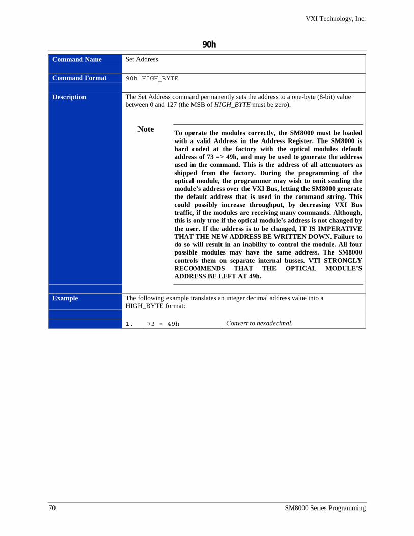
VXI Technology, Inc.
70 SM8000 Series Programming
90h Command Name Set Address Command Format 90h HIGH_BYTE
Description The Set Address command permanently sets the address to a one-byte (8-bit) value
between 0 and 127 (the MSB of HIGH_BYTE must be zero).
To operate the modules correctly, the SM8000 must be loaded with a valid Address in the Address Register. The SM8000 is hard coded at the factory with the optical modules default address of 73 => 49h, and may be used to generate the address used in the command. This is the address of all attenuators as shipped from the factory. During the programming of the optical module, the programmer may wish to omit sending the module’s address over the VXI Bus, letting the SM8000 generate the default address that is used in the command string. This could possibly increase throughput, by decreasing VXI Bus traffic, if the modules are receiving many commands. Although, this is only true if the optical module’s address is not changed by the user. If the address is to be changed, IT IS IMPERATIVE THAT THE NEW ADDRESS BE WRITTEN DOWN. Failure to do so will result in an inability to control the module. All four possible modules may have the same address. The SM8000 controls them on separate internal busses. VTI STRONGLY RECOMMENDS THAT THE OPTICAL MODULE’S ADDRESS BE LEFT AT 49h.
Example The following example translates an integer decimal address value into a
HIGH_BYTE format: 1. 73 = 49h Convert to hexadecimal.
Note
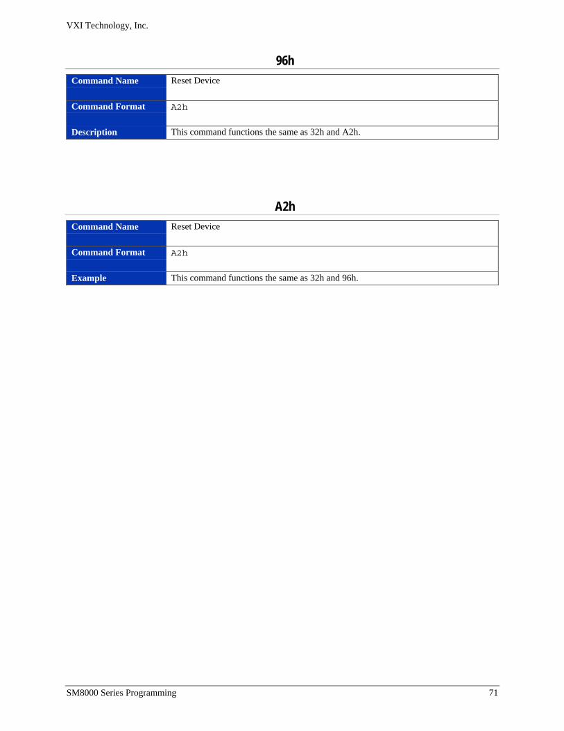
VXI Technology, Inc.
SM8000 Series Programming 71
96h Command Name Reset Device Command Format A2h
Description This command functions the same as 32h and A2h.
A2h Command Name Reset Device Command Format A2h
Example This command functions the same as 32h and 96h.

VXI Technology, Inc.
72 SM8000 Series Programming
VXI Technology, Inc.
SM8000 Series Index 73
INDEX
A
A16 address space.............................................................39 A16 base address ..............................................................37 A16 offset register ............................................................37 A16 offset register address ...............................................37 A24 address space.............................................................37 A24 base address ..............................................................37 A24/A32 active.................................................................39 A24/A32 enable ................................................................40 A24/A32 memory offset ...................................................40 A32 address space.............................................................37 A32 base address ..............................................................37 access LED fail bit............................................................49 ACFAILN enable bit ........................................................48 address space ..............................................................23, 39
B
backplane jumpers ............................................................21 BBM/MBB Bit .................................................................49 BBM/MBB Enable Bit .....................................................49
C
cable..................................................................................10 cause/status .......................................................................41 command parsing..............................................................37 configuration registers ......................................................48 cooling ..............................................................................21
D
data bus.............................................................................50 delay timer ........................................................................49 device class .......................................................................39 dynamic configuration ......................................................39
E
electric shock ................................................................9, 10 electrical overload...............................................................9 explosive atmosphere........................................................10 extended memory device ..................................................41 extended memory space....................................................23
F
firmware version number..................................................40 frame or chassis ground ......................................................9 front panel open signal set by this module........................51
G
grounding conductor.........................................................10
H
handler IRQ Line ..............................................................41 hardware revision code .............................51, 52, 53, 55, 56
I
IH ENA* .......................................................................... 41 interrupt mask .................................................................. 41 interrupter IRQ line .......................................................... 41 IR ENA* .......................................................................... 41 IRQ line............................................................................ 41
L
logical address................................................ 21, 22, 23, 39 LSB (least significant bit) .......................................... 22, 23
M
major hardware version number....................................... 40 manufacturer's ID............................................................. 39 memory space .................................................................. 48 message-based.................................................................. 37 minor hardware version number....................................... 40 model code ....................................................................... 39 MODID* .......................................................................... 39 module relay address........................................................ 54 MSB (most significant bit) ......................................... 22, 23
O
offset register.................................................................... 37 offset value....................................................................... 37 openbus out enable bit...................................................... 50 overheating....................................................................... 10
P
polled fashion................................................................... 41 power................................................................................ 21 power cord.................................................................... 9, 10 power source ...................................................................... 9 probes............................................................................... 10
R
rating fuse........................................................................... 9 register address................................................................. 37 registers ...................................................................... 37, 39 relay control ..................................................................... 54 relay data read back polarity bit ....................................... 48 relay register address.................................................. 54, 55 relay register offset........................................................... 54 relay reset enable bit ........................................................ 49 relay reset select bit.......................................................... 50 required memory .............................................................. 39 reset .................................................................................. 40
S
serial clock ....................................................................... 42 specified voltage ................................................................ 9 sysfail inhibit.................................................................... 40

VXI Technology, Inc.
74 SM8000 Series Index
T
temperature range .............................................................10 test leads ...........................................................................10 trigger ...............................................................................45
V
ventilation .........................................................................10 VXIbus .......................................................................21, 37 VXIbus Extended Device .................................................41
W
wet or damp conditions.....................................................10