Embed Size (px)
Citation preview
Application ReportSNVA678B–September 2012–Revised May 2013
AN-2296 SM72295: Highly Integrated Gate Driver for800VA to 3KVA Inverter
.....................................................................................................................................................
ABSTRACT
This application note describes the design principles and circuit operation of TI’s highly Integrated Gatedriver in the Low Frequency Inverters.
The inverter industry is expected to witness many technological innovations in the coming years to cater toa larger number of applications and new categories of end users. The demand from retail showrooms,small offices and residential use is primarily for 800VA, 1 kVA, 1.4 kVA and 2 kVA inverters. Being ahighly fragmented, competitive and growing market, it is in desperate need of constant Innovation andIntegration.
Contents1 Introduction .................................................................................................................. 2
1.1 Basics of Gate Drive Requirement .............................................................................. 21.2 Bootstrap circuit Principle for High Side Gate Drive ........................................................... 31.3 Low Frequency 600VA to 3KVA Pure Sine Wave Inverter Design .......................................... 4
2 SM72295– Achieving High Integration in Current LF Inverter Design ............................................... 72.1 Application Schematic — SM72295 in 800VA Pure Sine Wave Inverters ................................. 82.2 Easy Design Guidelines for Integrated Current Sensing ..................................................... 92.3 Layout Guidelines ................................................................................................ 10
3 Test Results in 850VA Pure Sine Wave Inverter Applications ...................................................... 113.1 Inverter Mode ..................................................................................................... 113.2 Charger Mode/Mains Mode ..................................................................................... 13
List of Figures
1 Simplified Model of a Non Inverting Gate Driver IC and a Power MOSFET ....................................... 2
2 A Closer Look of Driver Driving the MOSFET .......................................................................... 2
3 Power MOSFET Gate Drive Characteristics ............................................................................ 3
4 Bootstrap Supply Circuit ................................................................................................... 4
5 Inverter’s Block Diagram .................................................................................................. 5
6 Gate Drive Inputs in Inverter Mode ...................................................................................... 6
7 Inverter Mode Operation .................................................................................................. 6
8 Block Diagram of SM72295 Gate Driver ................................................................................ 7
9 SM72295 in 800VA pure Sine Wave Inverters.......................................................................... 8
10 Integrated Current Sensing Amplifier..................................................................................... 9
11 Inputs to Gate Driver in Inverter Mode with Load of 700VA ......................................................... 11
12 Signal Integrity from Input to Output Gate Drives in Low Side MOSFETs on 700VA Load in InverterMode. ....................................................................................................................... 12
13 Signal Integrity from Input to Output Gate Drives in High Side MOSFETs on 700VA Load in InverterMode ........................................................................................................................ 13
14 Inputs to Gate Driver in Mains Mode With AC Mains Input of 220V................................................ 14
15 Signal Integrity from Input to Output Gate Drives in Low Side MOSFETs in 220V AC Mains Mode........... 14
16 Signal Integrity from Input to Output Gate Drives in High Side MOSFETs in 220V AC Mains Mode. ......... 15All trademarks are the property of their respective owners.
1SNVA678B–September 2012–Revised May 2013 AN-2296 SM72295: Highly Integrated Gate Driver for 800VA to 3KVAInverterSubmit Documentation Feedback
Copyright © 2012–2013, Texas Instruments Incorporated
PWM
Driver
VCC
P
N
S
MOSFET
CDS
CGS
CGD
D
SW-Node
GTurn On
Turn Off
ControllerInput
GateDriver
Gate RG
CGD
CGS
LD
Drain
LS
CDS
Power MOSFET
Source
Introduction www.ti.com
1 Introduction
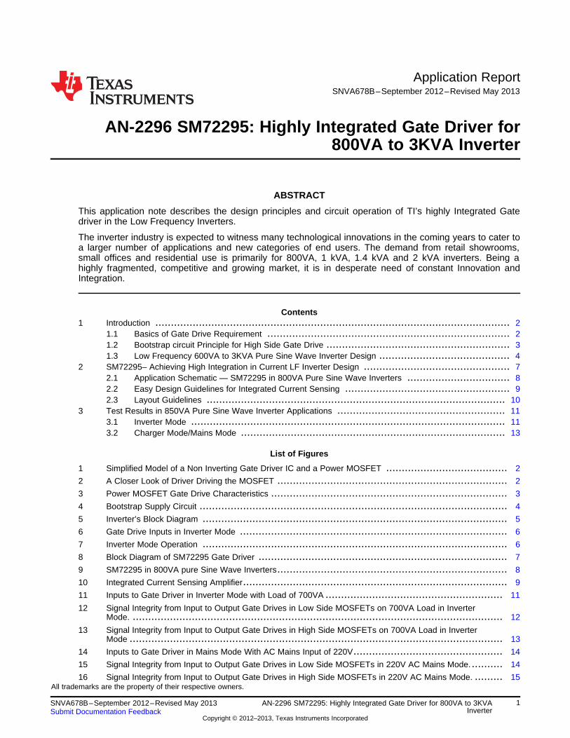
Gate Driver is a power amplifier that accepts a low-power input from a controller IC and produces theappropriate high-current gate drive for a power MOSFET. The gate driver must source and sink current toestablish required Vgs. A gate driver is used when a pulse width- modulation (PWM) controller cannotprovide the output current required to drive the gate capacitance of the MOSFET. Gate drivers may beimplemented as dedicated ICs, discrete transistors, or transformers. They can also be integrated within acontroller IC. Partitioning the gate-drive function off the PWM controller allows the controller to run coolerand be more stable by eliminating the high peak currents and heat dissipation needed to drive a powerMOSFET at very high frequencies.
1.1 Basics of Gate Drive Requirement
Figure 1. Simplified Model of a Non Inverting Gate Driver IC and a Power MOSFET
A Real MOSFET’s Properties
• Fundamentally a voltage controlled switch.
• Inherent parasitic capacitors.
• Rds(ON) is not negligible.
This leads to the requirement of Gate driver which must source and sink current to establish requiredthreshold voltage from Gate to Source Vgs.
Figure 2. A Closer Look of Driver Driving the MOSFET
2 AN-2296 SM72295: Highly Integrated Gate Driver for 800VA to 3KVA SNVA678B–September 2012–Revised May 2013Inverter Submit Documentation Feedback
Copyright © 2012–2013, Texas Instruments Incorporated

VS
G, G
ate-
To-
Sou
rce
Vol
tage
(V
)
QG, Total Gate Charge (nC)
www.ti.com Introduction
Figure 1 shows the simplified model, including the parasitic components that influence high-speedswitching, gate-to-source capacitance (CGS), the gate-to-drain capacitance (CGD), and drain-to-sourcecapacitance (CDS).Values of the source inductance (LS) and drain inductance (LD) depend on theMOSFET’s package. The other parasitic component is RG, the resistance associated with the gate signaldistribution within the MOSFET that affects switching times. An important attribute for the gate driver is itsability to provide sufficient drive current to quickly pass through the Miller Plateau Region of the power-MOSFET’s switching transition. This interval occurs when the transistor is being driven on or off, and thevoltage across its gate-to-drain parasitic capacitor (CGD) is being charged or discharged by the gatedriver. Figure 3 plots total gate charge as a function of the gate-drive voltage of a power MOSFET. Totalgate charge (QG) is how much must be supplied to the MOSFET gate. to achieve full turn-on. It is usuallyspecified in nanocoulombs (nC).
Figure 3. Power MOSFET Gate Drive Characteristics
1.2 Bootstrap circuit Principle for High Side Gate Drive
The gate drive requirements for a power MOSFET utilized as a high side switch, in applications like Fullbridge, half-bridge converters or synchronous buck converters can be summarized as follows:
• Gate voltage must be 6 to 12V higher than the source voltage. To fully enhance a high side switch, thegate to source voltage would have to be higher than the threshold voltage plus the minimum necessaryvoltage to fully enhance the MOSFET
• The gate voltage must be controllable from the logic level, which are normally referenced to ground.Thus, the control signals need to be level shifted to the source terminal of high side MOSFET (HSnode), which in most applications, swings between ground and the high voltage rail.
The Bootstrap supply technique is a simple, cost-effective way to power the upper MOSFET’s gate andprovide bias supply to the floating logic sections of the Gate Driver. Only two components (a Bootstrapdiode and capacitance) per bridge phase are needed to implement the Bootstrap supply.
3SNVA678B–September 2012–Revised May 2013 AN-2296 SM72295: Highly Integrated Gate Driver for 800VA to 3KVAInverterSubmit Documentation Feedback
Copyright © 2012–2013, Texas Instruments Incorporated

DC Supply
Load
Q1
Q2RG2
RG1VDD
VDD
VB
HO
VS
LOCOM
CBoot
DBootRBoot
ILoad
Bootstrap Charge Current Path
Bootstrap Discharge Current Path
Introduction www.ti.com
Figure 4. Bootstrap Supply Circuit
Using this circuit, the Bootstrap Capacitor is charged to ground through the Low side FET. When the Lowside FET is turned off, the bottom of the capacitor flies up and this creates a voltage greater than Vcc.This voltage is applied to the High side gate driver.
1.3 Low Frequency 600VA to 3KVA Pure Sine Wave Inverter Design
There is a dual mode of operation in a residential Inverter ie Mains mode and Inverter mode. As shown inFigure 5, the Input AC voltage is fed to the transformer through a switch (relay). In the mains mode, wheninput AC is present and is within valid range, the switch is closed and the input AC directly goes to theoutput load. The same AC is fed to transformer, and the H-bridge consisting of MOSFETs or IGBTs aredriven through microcontroller or DSP to charge the battery. A bridge less rectification principle is used tocharge the battery by boosting the voltage produced in the transformer primary using the inductance of thewinding, by switching the lower MOSFET banks. The lower MOSFET switches are switched and upperswitches kept turned OFF, The body diodes of the upper MOSFETS will act as rectifiers. The pulse widthof the switching pulses of the lower bank is proportional to the output charge current.
4 AN-2296 SM72295: Highly Integrated Gate Driver for 800VA to 3KVA SNVA678B–September 2012–Revised May 2013Inverter Submit Documentation Feedback
Copyright © 2012–2013, Texas Instruments Incorporated

Mains Input
Output Load
SwitchBattery Bank
DSP Control
Inverter Section
Power Stage Power Transformer
T15 1
3 4
C2
www.ti.com Introduction
Figure 5. Inverter’s Block Diagram
The DC/AC inversion can be achieved using any one of the two following methods.
The method in which the low voltage DC power is inverted, is completed in two steps. The first is theconversion of the low voltage DC power to a high voltage DC source, and the second step is theconversion of the high DC source to an AC waveform using pulse width modulation.
Another method to complete the desired outcome would be to first convert the low voltage DC power toAC, and then use a transformer to boost the voltage to 120/220 volts. The widely used method in thecurrent residential inverter is the second one . Here if the AC fails or is out of valid range (AC VoltageSense is required), the switch between Mains Input and Output Load opens. H-bridge circuit convertsbattery DC voltage into AC using high frequency PWM (5 kHz to 15 KHz) thus feeding the sametransformer which is being used for charging in the mains mode. The output of transformer contains acapacitor which filters it to make 50 Hz AC.
5SNVA678B–September 2012–Revised May 2013 AN-2296 SM72295: Highly Integrated Gate Driver for 800VA to 3KVAInverterSubmit Documentation Feedback
Copyright © 2012–2013, Texas Instruments Incorporated

OFF PWM PWM OFF
ON Complementary PWM Complementary PWM ON
1
5 8
4C1
T1
D3
D1 D2
D4
BAT+
Q3
Q4
RSENSE
Battery BT1
INV O/P
Q1
Q2
InputAC
Switch
INV O/P
L
N
Battery
W_Bridge
1
1 5
4 8
5 8
4C1
C2
T1
T1
D3
D1 D2
D4
BAT+
Q3
Q4
RSENSE
Battery BT1
INV O/P
Q1
Q2
15
10
5
0
-5
-10
-150 0.002 0.004 0.0080.006 0.01 0.012 0.014 0.016 0.018
Three Level PWM Signal
Introduction www.ti.com
Figure 6. Gate Drive Inputs in Inverter Mode
Figure 7. Inverter Mode Operation
For the Positive Half of the Sine Wave generation, Q2 is always high ,Q1 is always off , Q3 is applied with6.4KHz (6.4KHz to 20KHz) PWM corresponding to Positive Half cycle 50Hz sine wave and Q4 is appliedwith corresponding complementary (to Q3) PWM . For the Negative Half 50Hz sine wave generation , Q4is always high , Q3 is always off , Q1 is applied with 6.4KHz PWM corresponding to positive half cycle50Hz sine wave and Q2 is applied with Q1's complementary PWM .
6 AN-2296 SM72295: Highly Integrated Gate Driver for 800VA to 3KVA SNVA678B–September 2012–Revised May 2013Inverter Submit Documentation Feedback
Copyright © 2012–2013, Texas Instruments Incorporated
HIA
LIA
LIB
HIB
LOB
HSB
HSA
LOA
HOA
HBA
HBB
HOB
DRIVER
UVLO
LEVELSHIFT
DRIVER
VCCUVLO
DRIVER
DRIVER
UVLO
3V
VCCB
3V
3V
3V
PGOOD
PGND
3V
AGND
SIB
IOUT
SOB
SIA
IIN
SOA
VDDCLAMP
+
_
VDDCLAMP
VDD 3.3V/5V
VCCB
PGND
VCCA
OVS
+
-
OVP
VDD
VDD
200k
VDD
+
_
+_
+_
BOUT BIN
50k
50k
LEVELSHIFT
100V Bootstrap DiodeVCCA
Integrated Current Sensing Amplifiers
100V Bootstrap Diode
www.ti.com SM72295– Achieving High Integration in Current LF Inverter Design
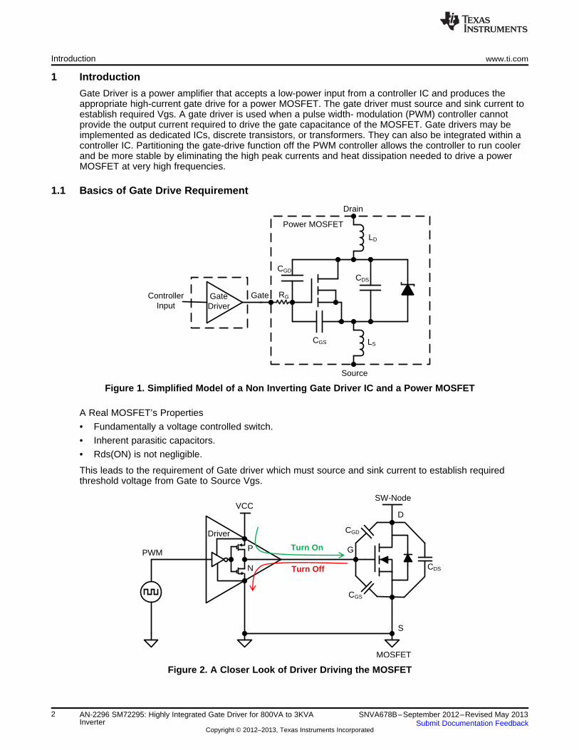
2 SM72295– Achieving High Integration in Current LF Inverter Design
The SM72295 is a full bridge MOSFET driver with 3A (higher no. of FETs in parallel for high power) peakcurrent drive capability with
1. Integrated ultra fast 100V boot strap diodes (can easily support up to 5KVA rated inverters)
2. Two high side current sense amplifiers with externally programmable gain and buffered outputs whichcan be used for measuring the Battery charge and discharge current – Additional current senseamplifiers and buffers are not required
3. Programmable over voltage protection – which can be used for Charge complete detection or for drivershutdown feature in case of a fault condition
4. Can be directly interfaced with a microcontroller
Figure 8. Block Diagram of SM72295 Gate Driver
7SNVA678B–September 2012–Revised May 2013 AN-2296 SM72295: Highly Integrated Gate Driver for 800VA to 3KVAInverterSubmit Documentation Feedback
Copyright © 2012–2013, Texas Instruments Incorporated

VD
D
SD
A
SIA
LIB
HIB
HIA
LIA
PG
D
OV
P
BIN
BO
UT
IIN IOU
T
AG
ND
VC
C1
VC
C2
SIB
SO
B
HB
A
HO
A
HS
A
LOA
LOB
HS
B
HO
B
HB
B
OV
S
AG
ND
17 2 1 9R
21
470
E
R25
4
70E
BLI
R26
4
70E
R22
4
70E
BH
I
AH
I
ALI
21
C12
VC
C
VD
D
C11
1µF
0.1µ
F
0.1µ
F
C10
25
R12
49
9ER
11
499E
C5
2.2µ
F/3
5V
C4
2200
µF
/35V
+C
322
00µ
F/3
5V
+
AP
AN
1mE
/2W
1mE
/2W
FU
SE
140
A
40A
FU
SE
2
Bat
tery
+
VC
C
VD
D
R19
220E
R20
1K
D5
12V
D6
3.3V
5
C23
1000
pFR
34
82K
123
C22
1000
pFR
33
39K
1141510678
C19
1000
pFC
1810
00pF
BIN
BO
UT
R24
1
K
R23
1
K
H B
ridge
Sw
itchi
ng W
avef
orm
Inpu
ts
gene
rate
d by
mic
oron
trol
ler
2316S
DR
28 1
00K
R27 1M
20C
15 0
.47µ
F
191822
HO
B
HS
B
LOB
LOA
HO
A
HS
A24282726
C14
0.4
7µF
1314
AP
AN
R15
499
E
R18
49
9E
Shu
tdow
n si
gnal
from
mic
roco
ntro
ller
All
the
outp
uts
will
be
disa
bled
if v
olta
ge a
t O
VS
>V
DD
ie 3
.3V
in th
is c
ase
BIN
= D
isch
argi
ng c
urre
nt in
inve
rter
mod
e (G
ain
= R
33/R
11)
BO
UT
= C
harg
ing
curr
ent i
n m
ains
mod
e (G
ain
= R
34/R
15)
Bot
h th
e cu
rren
t sen
se c
an d
irect
ly b
e in
terf
aced
to th
e A
DC
of m
icro
cont
rolle
r
LOAR
4510
EIN
4148
D3
A CLO
BR50
10E
A CIN41
48D
4
R44
47E
R41
47E
R42
47E
R43
10K
CS
D18
532K
CS
CS
D18
532K
CS
CS
D18
532K
CS
CS
D18
532K
CS
CS
D18
532K
CS
CS
D18
532K
CS
CS
D18
532K
CS
CS
D18
532K
CS
CS
D18
532K
CS
CS
D18
532K
CS
CS
D18
532K
CS
CS
D18
532K
CS
R48
10K
R49
47E
R46
47E
R47
47E
Q10
Q11
Q3
Q12
Q13
Q4
HO
AH
OB
R35
10E
R40
10E
R32
10K
R38
10K
HS
AH
SB
IN41
48D
1IN
4148
D2
AA
CC
R31
47E
R29
47E
R30
47E
R39
47E
R36
47E
R37
47E
Q7
Q6
Q1
Q8
Q9
Q2
U3
SM
7229
5
Bat
tery
+
Bat
tery
-
J1
J2
1 2
Bat
tery
+ 1 2 3 4
SM72295– Achieving High Integration in Current LF Inverter Design www.ti.com
2.1 Application Schematic — SM72295 in 800VA Pure Sine Wave Inverters
Figure 9. SM72295 in 800VA pure Sine Wave Inverters
8 AN-2296 SM72295: Highly Integrated Gate Driver for 800VA to 3KVA SNVA678B–September 2012–Revised May 2013Inverter Submit Documentation Feedback
Copyright © 2012–2013, Texas Instruments Incorporated
+
BPI
Discharge ChargeShunt
LOAD/Charger
Gain = RC2/RC1
Charge Current Signal
RC2RC1
RC1SOB
SIBIOUT
SIA
SOAIIN
RD1
RD1RD2
Gain = RD2/RD1
Discharge Current Signal
Voltage Source
RSENSE
VSENSE ISENSE
LOADRR
SIA SOA
Drop Across R is VSENSE
Current Through FET is VSENSE/R
P Channel FET
Current Sense AmplifierIOUT
R0
V0 = (VSENSE*R0)/R
SIA SOA IN
VDD CLAMP
BIN
BOUT
+
+
SIB SOB OUT
+
+
VDD CLAMP
+
+
www.ti.com SM72295– Achieving High Integration in Current LF Inverter Design
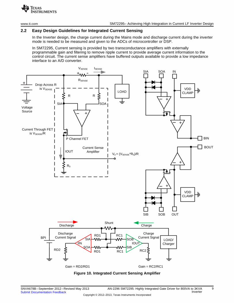
2.2 Easy Design Guidelines for Integrated Current Sensing
In the Inverter design, the charge current during the Mains mode and discharge current during the invertermode is needed to be measured and given to the ADCs of microcontroller or DSP.
In SM72295, Current sensing is provided by two transconductance amplifiers with externallyprogrammable gain and filtering to remove ripple current to provide average current information to thecontrol circuit. The current sense amplifiers have buffered outputs available to provide a low impedanceinterface to an A/D converter.
Figure 10. Integrated Current Sensing Amplifier
9SNVA678B–September 2012–Revised May 2013 AN-2296 SM72295: Highly Integrated Gate Driver for 800VA to 3KVAInverterSubmit Documentation Feedback
Copyright © 2012–2013, Texas Instruments Incorporated

SM72295– Achieving High Integration in Current LF Inverter Design www.ti.com
Hence the charge and the discharge current can easily be measured by giving individual gain to each ofthem. The charging current is generally pretty less than the possible Discharging current in 800VA LowFrequency inverter. The Maximum charging current for 150-165AH battery is close to 15A while thedischarging current can goes upto 60A-70A.
2.2.1 Steps of Current Sense Design1. Current Sense Resistance is chosen based on Max current and respective power dissipation on
Current Sense resistance. In this Design, two 2W 1 milliohm resistances in parallel were chosen sothat even at 70A Discharge current in Inverter mode, the power dissipation is 2.45W which is muchlesser than allowed 4W(2W each of parallel 1milliohm Resistance).
2. There is VDD (3.3V) clamped at the Current Sense amplifier output and hence the gain should bemaintained in such a way that the output is not clamped in the area of interest. The Discharge currentgain is achieved through R33 / R11 (refer to application Schematic) which comes out to be the gain of78 in this application. Even at 70A discharge current, the BIN= 2.73V which is lower than VDD clamp.
3. Since the Maximum Charge current in this application is close to 15A, the gain of this section ismaintained higher through R34/R15 ratio.
2.3 Layout Guidelines
The optimum performance of high and low-side gate drivers cannot be achieved without taking dueconsiderations during circuit board layout. Following points are emphasized.
1. Low ESR / ESL capacitors must be connected close to the IC, between VDD and VSS pins andbetween the HB and HS pins to support the high peak currents being drawn from VDD during turn-onof the external MOSFET.
2. To prevent large voltage transients at the drain of the top MOSFET, a low ESR electrolytic capacitormust be connected between MOSFET drain and ground (VSS).
3. In order to avoid large negative transients on the switch node (HS pin), the parasitic inductances in thesource of top MOSFET and in the drain of the bottom MOSFET (synchronous rectifier) must beminimized.
4. Grounding Considerations
(a) The first priority in designing Grounding Consideration is a part in layout Guidelines. connections isto confine the high peak currents that charge and discharge the MOSFET gate into a minimalphysical area. This will decrease the loop inductance and minimize noise issues on the gateterminal of the MOSFET. The MOSFETs should be placed as close as possible to the gate driver.
(b) The second high current path includes the Bootstrap capacitor, the Bootstrap diode, the localground referenced bypass capacitor and low-side MOSFET body diode. The Bootstrap capacitor isrecharged on a cycle-by-cycle basis through the Bootstrap diode from the ground referenced VDDbypass capacitor. The recharging occurs in a short time interval and involves high peak current.Minimizing this loop length and area on the circuit board is important to ensure reliable operation.
10 AN-2296 SM72295: Highly Integrated Gate Driver for 800VA to 3KVA SNVA678B–September 2012–Revised May 2013Inverter Submit Documentation Feedback
Copyright © 2012–2013, Texas Instruments Incorporated
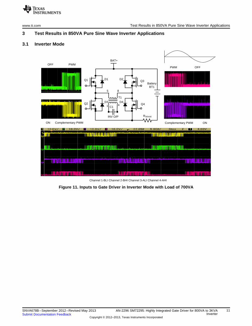
Channel 1-BLI Channel 2-BHI Channel 3-ALI Channel 4-AHI
OFF PWMPWM OFF
ON Complementary PWM Complementary PWM ON
1
5 8
4C1
T1
D3
D1 D2
D4
BAT+
Q3
Q4
RSENSE
Battery BT1
INV O/P
Q1
Q2
www.ti.com Test Results in 850VA Pure Sine Wave Inverter Applications
3 Test Results in 850VA Pure Sine Wave Inverter Applications
3.1 Inverter Mode
Figure 11. Inputs to Gate Driver in Inverter Mode with Load of 700VA
11SNVA678B–September 2012–Revised May 2013 AN-2296 SM72295: Highly Integrated Gate Driver for 800VA to 3KVAInverterSubmit Documentation Feedback
Copyright © 2012–2013, Texas Instruments Incorporated

Channel 1-ALI Channel 2-ALO Channel 3-BLI Channel 4-BLO
Test Results in 850VA Pure Sine Wave Inverter Applications www.ti.com
Figure 12. Signal Integrity from Input to Output Gate Drives in Low Side MOSFETs on 700VA Load inInverter Mode.
12 AN-2296 SM72295: Highly Integrated Gate Driver for 800VA to 3KVA SNVA678B–September 2012–Revised May 2013Inverter Submit Documentation Feedback
Copyright © 2012–2013, Texas Instruments Incorporated

Channel 1- Probe Across BHO and BHS
Channel 1- BHO Channel 2-BHS Channel 3- BHI Channel between 1 and 2 ± Maths 1-2 for VGS
www.ti.com Test Results in 850VA Pure Sine Wave Inverter Applications
Figure 13. Signal Integrity from Input to Output Gate Drives in High Side MOSFETs on 700VA Load inInverter Mode
3.2 Charger Mode/Mains Mode1. During Mains mode, the same transformer which is used in DC/AC inversion by boosting battery
voltage to line voltage in inverter mode, is connected to the mains power using a relay. A bridge lessrectification principle is used to charge the battery by boosting the voltage produced in the transformerprimary using the inductance of the winding, by switching the lower MOSFET banks..
2. The lower MOSFET switches are switched and upper switches kept turned OFF, The body diodes ofthe upper MOSFETS will act as rectifiers. The pulse width of the switching pulses of the lower bank isproportional to the output charge current.
13SNVA678B–September 2012–Revised May 2013 AN-2296 SM72295: Highly Integrated Gate Driver for 800VA to 3KVAInverterSubmit Documentation Feedback
Copyright © 2012–2013, Texas Instruments Incorporated

Channel 1-BLI Chanel 2-BLO Channel 3-ALI Channel 4-ALO
Channel 1 ± BLI Channel 2-BHI Channel 3-ALI Channel 4-AHI
Test Results in 850VA Pure Sine Wave Inverter Applications www.ti.com
Figure 14. Inputs to Gate Driver in Mains Mode With AC Mains Input of 220V
Figure 15. Signal Integrity from Input to Output Gate Drives in Low Side MOSFETs in 220V AC MainsMode.
14 AN-2296 SM72295: Highly Integrated Gate Driver for 800VA to 3KVA SNVA678B–September 2012–Revised May 2013Inverter Submit Documentation Feedback
Copyright © 2012–2013, Texas Instruments Incorporated

www.ti.com Test Results in 850VA Pure Sine Wave Inverter Applications
Figure 16. Signal Integrity from Input to Output Gate Drives in High Side MOSFETs in 220V AC MainsMode.
15SNVA678B–September 2012–Revised May 2013 AN-2296 SM72295: Highly Integrated Gate Driver for 800VA to 3KVAInverterSubmit Documentation Feedback
Copyright © 2012–2013, Texas Instruments Incorporated

IMPORTANT NOTICETexas Instruments Incorporated and its subsidiaries (TI) reserve the right to make corrections, enhancements, improvements and otherchanges to its semiconductor products and services per JESD46, latest issue, and to discontinue any product or service per JESD48, latestissue. Buyers should obtain the latest relevant information before placing orders and should verify that such information is current andcomplete. All semiconductor products (also referred to herein as “components”) are sold subject to TI’s terms and conditions of salesupplied at the time of order acknowledgment.TI warrants performance of its components to the specifications applicable at the time of sale, in accordance with the warranty in TI’s termsand conditions of sale of semiconductor products. Testing and other quality control techniques are used to the extent TI deems necessaryto support this warranty. Except where mandated by applicable law, testing of all parameters of each component is not necessarilyperformed.TI assumes no liability for applications assistance or the design of Buyers’ products. Buyers are responsible for their products andapplications using TI components. To minimize the risks associated with Buyers’ products and applications, Buyers should provideadequate design and operating safeguards.TI does not warrant or represent that any license, either express or implied, is granted under any patent right, copyright, mask work right, orother intellectual property right relating to any combination, machine, or process in which TI components or services are used. Informationpublished by TI regarding third-party products or services does not constitute a license to use such products or services or a warranty orendorsement thereof. Use of such information may require a license from a third party under the patents or other intellectual property of thethird party, or a license from TI under the patents or other intellectual property of TI.Reproduction of significant portions of TI information in TI data books or data sheets is permissible only if reproduction is without alterationand is accompanied by all associated warranties, conditions, limitations, and notices. TI is not responsible or liable for such altereddocumentation. Information of third parties may be subject to additional restrictions.Resale of TI components or services with statements different from or beyond the parameters stated by TI for that component or servicevoids all express and any implied warranties for the associated TI component or service and is an unfair and deceptive business practice.TI is not responsible or liable for any such statements.Buyer acknowledges and agrees that it is solely responsible for compliance with all legal, regulatory and safety-related requirementsconcerning its products, and any use of TI components in its applications, notwithstanding any applications-related information or supportthat may be provided by TI. Buyer represents and agrees that it has all the necessary expertise to create and implement safeguards whichanticipate dangerous consequences of failures, monitor failures and their consequences, lessen the likelihood of failures that might causeharm and take appropriate remedial actions. Buyer will fully indemnify TI and its representatives against any damages arising out of the useof any TI components in safety-critical applications.In some cases, TI components may be promoted specifically to facilitate safety-related applications. With such components, TI’s goal is tohelp enable customers to design and create their own end-product solutions that meet applicable functional safety standards andrequirements. Nonetheless, such components are subject to these terms.No TI components are authorized for use in FDA Class III (or similar life-critical medical equipment) unless authorized officers of the partieshave executed a special agreement specifically governing such use.Only those TI components which TI has specifically designated as military grade or “enhanced plastic” are designed and intended for use inmilitary/aerospace applications or environments. Buyer acknowledges and agrees that any military or aerospace use of TI componentswhich have not been so designated is solely at the Buyer's risk, and that Buyer is solely responsible for compliance with all legal andregulatory requirements in connection with such use.TI has specifically designated certain components as meeting ISO/TS16949 requirements, mainly for automotive use. In any case of use ofnon-designated products, TI will not be responsible for any failure to meet ISO/TS16949.Products ApplicationsAudio www.ti.com/audio Automotive and Transportation www.ti.com/automotiveAmplifiers amplifier.ti.com Communications and Telecom www.ti.com/communicationsData Converters dataconverter.ti.com Computers and Peripherals www.ti.com/computersDLP® Products www.dlp.com Consumer Electronics www.ti.com/consumer-appsDSP dsp.ti.com Energy and Lighting www.ti.com/energyClocks and Timers www.ti.com/clocks Industrial www.ti.com/industrialInterface interface.ti.com Medical www.ti.com/medicalLogic logic.ti.com Security www.ti.com/securityPower Mgmt power.ti.com Space, Avionics and Defense www.ti.com/space-avionics-defenseMicrocontrollers microcontroller.ti.com Video and Imaging www.ti.com/videoRFID www.ti-rfid.comOMAP Applications Processors www.ti.com/omap TI E2E Community e2e.ti.comWireless Connectivity www.ti.com/wirelessconnectivity
Mailing Address: Texas Instruments, Post Office Box 655303, Dallas, Texas 75265Copyright © 2014, Texas Instruments Incorporated