Embed Size (px)
Citation preview

SGUS036B − JULY 2003 − REVISED OCTOBER 2003
1POST OFFICE BOX 1443 • HOUSTON, TEXAS 77251−1443
Controlled Baseline− One Assembly/Test Site, One Fabrication
Site
Extended Temperature Performance of−55°C to 125°C
Enhanced Diminishing ManufacturingSources (DMS) Support
Enhanced Product-Change Notification
Qualification Pedigree †
High-Performance Static CMOS Technology− 25-ns Instruction Cycle Time (40 MHz)− 40-MIPS Performance− Low-Power 3.3-V Design
Based on TMS320C2xx DSP CPU Core− Code-Compatible With F243/F241/C242− Instruction Set and Module Compatible
With F240/C240 On-Chip Memory
− 32K Words x 16 Bits of Flash EEPROM (4 Sectors) or ROM
− Programmable “Code-Security” Featurefor the On-Chip Flash/ROM
− Up to 2.5K Words x 16 Bits ofData/Program RAM− 544 Words of Dual-Access RAM− 2K Words of Single-Access RAM
Boot ROM− SCI/SPI Bootloader
External Memory Interface− 192K Words x 16 Bits of Total Memory:
64K Program, 64K Data, 64K I/O
Watchdog (WD) Timer Module
10-Bit Analog-to-Digital Converter (ADC)− 8 or 16 Multiplexed Input Channels− 375 ns or 500 ns MIN Conversion Time− Selectable Twin 8-State Sequencers
Triggered by Two Event Managers
Controller Area Network (CAN) 2.0B Module
Serial Communications Interface (SCI)
16-Bit Serial Peripheral Interface (SPI)
Two Event-Manager (EV) Modules(EVA and EVB), Each Includes:− Two 16-Bit General-Purpose Timers− Eight 16-Bit Pulse-Width Modulation
(PWM) Channels Which Enable:− Three-Phase Inverter Control− Center- or Edge-Alignment of PWM
Channels− Emergency PWM Channel Shutdown
With External PDPINTx Pin− Programmable Deadband (Deadtime)
Prevents Shoot-Through Faults− Three Capture Units for Time-Stamping
of External Events− Input Qualifier for Select Pins− On-Chip Position Encoder Interface
Circuitry− Synchronized A-to-D Conversion− Designed for AC Induction, BLDC,
Switched Reluctance, and Stepper MotorControl
− Applicable for Multiple Motor and/orConverter Control
Phase-Locked-Loop (PLL)-Based ClockGeneration
40 Individually Programmable, MultiplexedGeneral-Purpose Input/Output (GPIO) Pins
Five External Interrupts (Power DriveProtection, Reset, Two Maskable Interrupts)
Power Management:− Three Power-Down Modes− Ability to Power Down Each Peripheral
Independently
Real-Time JTAG-Compliant Scan-BasedEmulation, IEEE Standard 1149.1 ‡ (JTAG)
Development Tools Include:− Texas Instruments (TI) ANSI C Compiler,
Assembler/Linker, and Code ComposerStudio Debugger
− Evaluation Modules− Scan-Based Self-Emulation (XDS510 )− Broad Third-Party Digital Motor Control
Support
Copyright 2003, Texas Instruments Incorporated
Please be aware that an important notice concerning availability, standard warranty, and use in critical applications ofTexas Instruments semiconductor products and disclaimers thereto appears at the end of this data sheet.
Code Composer Studio and XDS510 are trademarks of Texas Instruments.Other trademarks are the property of their respective owners.† Component qualification in accordance with JEDEC and industry standards to ensure reliable operation over an extended temperature range.
This includes, but is not limited to, Highly Accelerated Stress Test (HAST) or biased 85/85, temperature cycle, autoclave or unbiased HAST,electromigration, bond intermetallic life, and mold compound life. Such qualification testing should not be viewed as justifying use of thiscomponent beyond specified performance and environmental limits.
‡ IEEE Standard 1149.1−1990, IEEE Standard Test-Access Port
!" #!$% &"' &! #" #" (" " ") !"&& *+' &! #", &" ""%+ %!&"", %% #""'
SGUS036B − JULY 2003 − REVISED OCTOBER 2003
2 POST OFFICE BOX 1443 • HOUSTON, TEXAS 77251−1443
Description 3. . . . . . . . . . . . . . . . . . . . . . . . . . . . . . . . . . . . . 240xA Device Summary 4. . . . . . . . . . . . . . . . . . . . . . . . . . Functional Block Diagram of the 2407A
DSP Controller 5. . . . . . . . . . . . . . . . . . . . . . . . . . . . . . Pinouts 6. . . . . . . . . . . . . . . . . . . . . . . . . . . . . . . . . . . . . . . . Pin Functions 7. . . . . . . . . . . . . . . . . . . . . . . . . . . . . . . . . . . Memory Maps 14. . . . . . . . . . . . . . . . . . . . . . . . . . . . . . . . . Peripheral Memory Map of the 2407A/2406A 15. . . . . . . Device Reset and Interrupts 16. . . . . . . . . . . . . . . . . . . . . DSP CPU Core 20. . . . . . . . . . . . . . . . . . . . . . . . . . . . . . . . 240xA Instruction Set 20. . . . . . . . . . . . . . . . . . . . . . . . . . . Scan-Based Emulation 20. . . . . . . . . . . . . . . . . . . . . . . . . . Functional Block Diagram of the 2407A DSP CPU 21. . Internal Memory 28. . . . . . . . . . . . . . . . . . . . . . . . . . . . . . . . Peripherals 31. . . . . . . . . . . . . . . . . . . . . . . . . . . . . . . . . . . .
Event Manager Modules (EVA, EVB) 31. . . . . . . . . . . . Enhanced Analog-to-Digital Converter
(ADC) Module 35. . . . . . . . . . . . . . . . . . . . . . . . . . . .
Controller Area Network (CAN) Module 37. . . . . . . . . . Serial Communications Interface (SCI) Module 39. . . . Serial Peripheral Interface (SPI) Module 41. . . . . . . . . . PLL-Based Clock Module 43. . . . . . . . . . . . . . . . . . . . . . Digital I/O and Shared Pin Functions 46. . . . . . . . . . . . . External Memory Interface (LF2407A) 49. . . . . . . . . . . . Watchdog (WD) Timer Module 50. . . . . . . . . . . . . . . . . .
Development Support 53. . . . . . . . . . . . . . . . . . . . . . . . . . . Documentation Support 56. . . . . . . . . . . . . . . . . . . . . . . . . Electrical Specifications Data 57. . . . . . . . . . . . . . . . . . . . Absolute Maximum Ratings 57. . . . . . . . . . . . . . . . . . . . . . Device Operating Life 57. . . . . . . . . . . . . . . . . . . . . . . . . . . Recommended Operating Conditions 59. . . . . . . . . . . . . Parameter Measurement Information 63. . . . . . . . . . . . . . Migrating From 240x Devices to 240xA Devices 95. . . . Peripheral Register Description 96. . . . . . . . . . . . . . . . . . . Mechanical Data 109. . . . . . . . . . . . . . . . . . . . . . . . . . . . . .
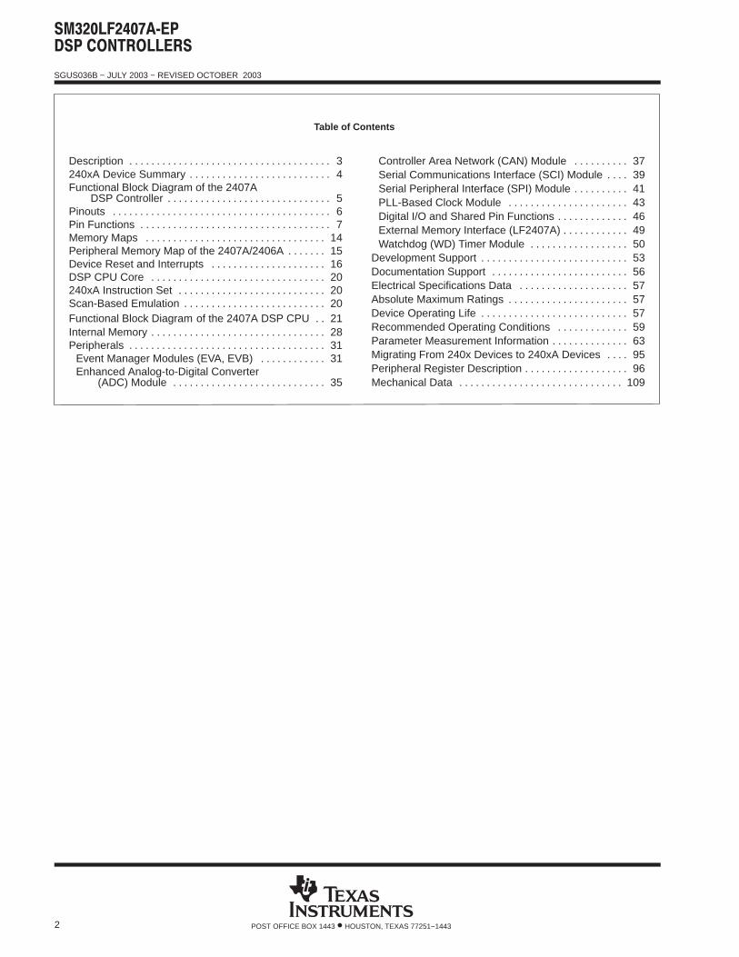
Table of Contents
SGUS036B − JULY 2003 − REVISED OCTOBER 2003
3POST OFFICE BOX 1443 • HOUSTON, TEXAS 77251−1443
description
The SM320LF2407A-EP is a member of the TMS320C24x generation of digital signal processor (DSP)controllers, and is part of the TMS320C2000 platform of fixed-point DSPs. The 240xA devices offer theenhanced TMS320 DSP architectural design of the C2xx core CPU for low-cost, low-power, andhigh-performance processing capabilities. Several advanced peripherals, optimized for digital motor andmotion control applications, have been integrated to provide a true single-chip DSP controller. Whilecode-compatible with the existing C24x DSP controller devices, the 2407A offers increased processingperformance (40 MIPS) and a higher level of peripheral integration. See the TMS320x240xA Device Summarysection for device-specific features.
The 240xA generation offers an array of memory sizes and different peripherals tailored to meet the specificprice/performance points required by various applications. Flash devices of up to 32K words offer acost-effective reprogrammable solution for volume production. The 240xA devices offer a password-based“code security” feature which is useful in preventing unauthorized duplication of proprietary code stored inon-chip Flash/ROM. Note that Flash-based devices contain a 256-word boot ROM to facilitate in-circuitprogramming. The 240xA family also includes ROM devices that are fully pin-to-pin compatible with their Flashcounterparts.
All 240xA devices offer at least one event manager module which has been optimized for digital motor controland power conversion applications. Capabilities of this module include center- and/or edge-aligned PWMgeneration, programmable deadband to prevent shoot-through faults, and synchronized analog-to-digitalconversion. Devices with dual event managers enable multiple motor and/or converter control with a single240xA DSP controller. Select EV pins have been provided with an “input-qualifier” circuitry, which minimizesinadvertent pin-triggering by glitches.
The high-performance, 10-bit analog-to-digital converter (ADC) has a minimum conversion time of 375 ns andoffers up to 16 channels of analog input. The autosequencing capability of the ADC allows a maximum of16 conversions to take place in a single conversion session without any CPU overhead.
A serial communications interface (SCI) is integrated on all devices to provide asynchronous communicationto other devices in the system. For systems requiring additional communication interfaces, the 2407A offers a16-bit synchronous serial peripheral interface (SPI). The 2407A offers a controller area network (CAN)communications module that meets 2.0B specifications. To maximize device flexibility, functional pins are alsoconfigurable as general-purpose inputs/outputs (GPIOs).
To streamline development time, JTAG-compliant scan-based emulation has been integrated into all devices.This provides non-intrusive real-time capabilities required to debug digital control systems. A complete suiteof code-generation tools from C compilers to the industry-standard Code Composer Studio debuggersupports this family. Numerous third-party developers not only offer device-level development tools, but alsosystem-level design and development support.
TMS320C24x, TMS320C2000, TMS320, and C24x are trademarks of Texas Instruments.
SGUS036B − JULY 2003 − REVISED OCTOBER 2003
4 POST OFFICE BOX 1443 • HOUSTON, TEXAS 77251−1443
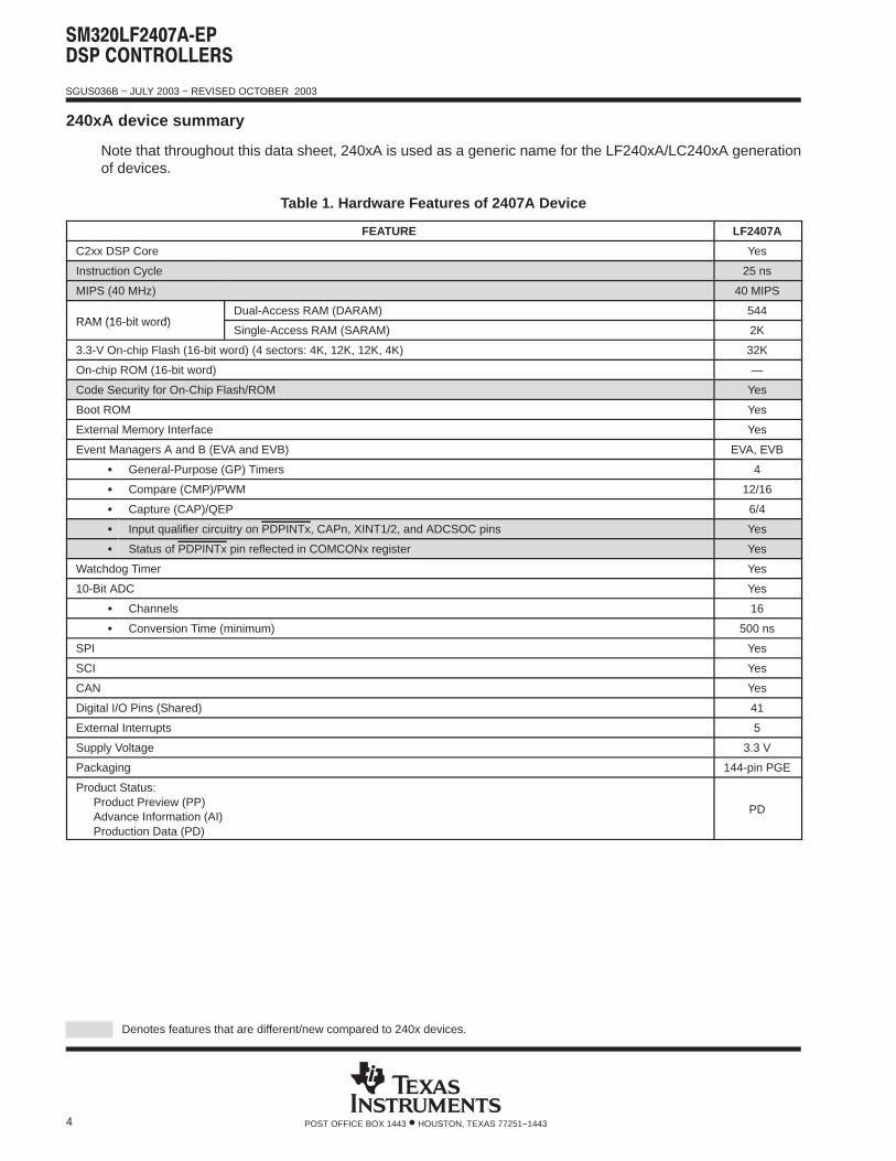
240xA device summary
Note that throughout this data sheet, 240xA is used as a generic name for the LF240xA/LC240xA generationof devices.
Table 1. Hardware Features of 2407A Device
FEATURE LF2407A
C2xx DSP Core Yes
Instruction Cycle 25 ns
MIPS (40 MHz) 40 MIPS
RAM (16-bit word)Dual-Access RAM (DARAM) 544
RAM (16-bit word)Single-Access RAM (SARAM) 2K
3.3-V On-chip Flash (16-bit word) (4 sectors: 4K, 12K, 12K, 4K) 32K
On-chip ROM (16-bit word) —
Code Security for On-Chip Flash/ROM Yes
Boot ROM Yes
External Memory Interface Yes
Event Managers A and B (EVA and EVB) EVA, EVB
General-Purpose (GP) Timers 4
Compare (CMP)/PWM 12/16
Capture (CAP)/QEP 6/4
Input qualifier circuitry on PDPINTx, CAPn, XINT1/2, and ADCSOC pins Yes
Status of PDPINTx pin reflected in COMCONx register Yes
Watchdog Timer Yes
10-Bit ADC Yes
Channels 16
Conversion Time (minimum) 500 ns
SPI Yes
SCI Yes
CAN Yes
Digital I/O Pins (Shared) 41
External Interrupts 5
Supply Voltage 3.3 V
Packaging 144-pin PGE
Product Status:Product Preview (PP)Advance Information (AI)Production Data (PD)
PD
Denotes features that are different/new compared to 240x devices.
SGUS036B − JULY 2003 − REVISED OCTOBER 2003
5POST OFFICE BOX 1443 • HOUSTON, TEXAS 77251−1443
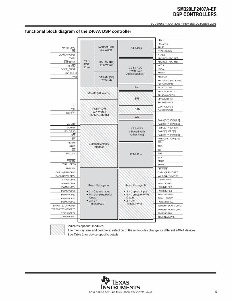
functional block diagram of the 2407A DSP controller
XTAL1/CLKIN
XTAL2
PLLVCCAPLLF2
PLLF
VSSAVREFHI
ADCIN08−ADCIN15VCCA
ADCIN00−ADCIN07
SCIRXD/IOPA1
SPISIMO/IOPC2
XINT2/ADCSOC/IOPD0
SCITXD/IOPA0
VREFLO
Port A(0−7) IOPA[0:7]
SPICLK/IOPC4
SPISTE/IOPC5
SPISOMI/IOPC3
Port E(0−7) IOPE[0:7]
Port F(0−6) IOPF[0:6]
Port C(0−7) IOPC[0:7]
Port D(0) IOPD[0]
Port B(0−7) IOPB[0:7]
TDO
TDI
CANRX/IOPC7
TRST
CANTX/IOPC6
EMU1
PDPINTB
TCK
EMU0
TMS
CAP5/QEP4/IOPF0
CAP4/QEP3/IOPE7
PWM7/IOPE1
PWM8/IOPE2
CAP6/IOPF1
PWM10/IOPE4
PWM9/IOPE3
PWM11/IOPE5
PWM12/IOPE6
T4PWM/T4CMP/IOPF3
T3PWM/T3CMP/IOPF2
TDIRB/IOPF4
TCLKINB/IOPF5
DARAM (B0)256 Words
DARAM (B1)256 Words
DARAM (B2)32 Words
C2xxDSPCore
PLL Clock
10-Bit ADC(With Twin
Autosequencer)
ÈÈÈÈÈÈÈÈÈÈÈÈÈÈÈÈÈÈÈÈÈÈÈÈÈÈÈÈÈÈÈÈÈÈÈ
ÈÈÈÈÈÈÈÈÈÈÈÈÈÈÈÈÈÈÈÈÈÈÈÈÈÈÈÈÈÈÈÈÈÈÈÈÈÈÈÈÈÈÈÈÈÈÈÈÈÈÈÈÈÈÈÈÈÈÈÈÈÈÈÈÈÈÈÈÈÈÈ
ÈÈÈÈÈÈÈÈÈÈÈÈÈÈÈÈÈÈÈÈÈÈÈÈÈÈÈÈÈÈÈÈÈÈÈÈÈÈÈÈÈÈÈÈÈÈÈÈÈÈÈÈÈÈÈÈÈÈÈÈÈÈÈ
RS
CLKOUT/IOPE0
XINT1/IOPA2
BIO/IOPC1
MP/MC
TMS2
A0−A15
D0−D15
TP1
TP2
BOOT_EN/XF
READY
STRB
R/W
RD
PS, DS, IS
VIS_OE
ENA_144
WE
CAP3/IOPA5
PWM1/IOPA6
CAP1/QEP1/IOPA3
CAP2/QEP2/IOPA4
PDPINTA
PWM5/IOPB2
PWM6/IOPB3
PWM3/IOPB0
PWM4/IOPB1
PWM2/IOPA7
T2PWM/T2CMP/IOPB5
T1PWM/T1CMP/IOPB4
TCLKINA/IOPB7
TDIRA/IOPB6
VDD (3.3 V)
VSS
VCCP(5V)
ÈÈÈÈÈÈÈÈÈÈÈÈÈÈÈÈÈÈÈÈÈÈÈÈÈÈÈÈÈÈÈÈÈÈÈÈÈÈÈÈÈÈÈÈÈÈÈÈÈÈÈÈÈÈÈÈÈÈÈÈÈÈÈÈÈÈÈÈÈÈÈÈ
SARAM (2K Words)
Flash/ROM(32K Words:
4K/12K/12K/4K)
External MemoryInterface
Event Manager A
3 × Capture Input 6 × Compare/PWM
Output 2 × GP
Timers/PWM
SCI
SPI
WD
Digital I/O(Shared WithOther Pins)
CAN
JTAG Port
Event Manager B
3 × Capture Input 6 × Compare/PWM
Output 2 × GP
Timers/PWM
ÈÈÈÈÈÈÈÈÈ
Indicates optional modules.The memory size and peripheral selection of these modules change for different 240xA devices.See Table 1 for device-specific details.
W/R / IOPC0
SGUS036B − JULY 2003 − REVISED OCTOBER 2003
6 POST OFFICE BOX 1443 • HOUSTON, TEXAS 77251−1443
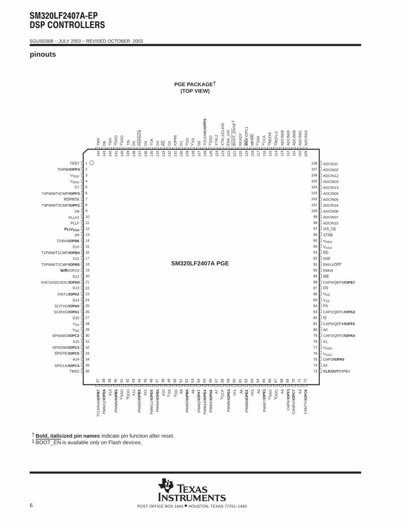
pinouts
144
143
142
141
140
139
138
137
136
135
134
RS
133
132
131
130
129
128
127
126
125
124
123
122
121
120
119
118
117
116
115
114
113
112
37 38 39 40 41 42 43 44 45 46 47 48 49 50 51 52 53 54 55 56 57 58 59 60 61 62 63 64 65 66 67 68 69
1
2
3
4
5
6
7
8
9
10
11
12
13
14
15
16
17
18
19
20
21
22
23
24
25
26
27
28
29
30
31
32
33
34
35
36
108
107
106
105
104
103
102
101
100
99
98
97
96
95
94
93
92
91
90
89
88
87
86
85
84
83
82
81
80
79
78
77
76
75
74
73
111
110
109
70 71 72
SM320LF2407A PGE
PDPINTA
PLLF
TDIRA/IOPB6
XINT2/ADCSOC/IOPD0
CLKOUT /IOPE0
PD
PIN
TB
XTA
L1/C
LKIN
XTA
L2
PLLVCCA
PLLF2
BO
OT
_EN
/XF
CC
PV
TP
1
TP
2
IOP
F6
EMU0
EMU1/OFF
TC
K
TD
I
TD
O
TM
S
TMS2
TRST
DS
IS
PS
R/W
W/R/IOPC0
RD
WE
STRBR
EA
DY
MP
/MC
EN
A_1
44VIS_OE
A0
A1
A2
A3
A4
A5
A6
A7
A8
A9
A10
A11
A12
A13
A14
A15
D0
D1
D2
D3
D4
D5
D6
D7
D8
D9
D10
D11
D12
D13
D14
D15
PLLVCCA
VDD
DD
V
VDD
DD
VVDDO
DD
OV
DD
OV
VDDO
VDDO
DD
OV
VSS
SS
V
VSS
SS
V
VSSO
SS
OV
SS
OV
VSSO
VSSO
SS
OV
SS
OV
CAP1/QEP1/IOPA3
CAP2/QEP2/IOPA4
CAP3/IOPA5
PW
M1/
PW
M2/
PW
M3/
PW
M4/
PW
M5/
PW
M6/
T1PWM/T1CMP/IOPB4
T2PWM/T2CMP/IOPB5
TC
LKIN
A/
CAP4/QEP3/IOPE7
CAP5/QEP4/IOPF0
CA
P6/
PW
M7/
PW
M8/
PW
M9/
PW
M10
/
PW
M11
/
PW
M12
/
T3PWM/T3CMP/IOPF2
T4PWM/T4CMP/IOPF3
TDIRB/IOPF4
TC
LKIN
B/
AD
CIN
00
AD
CIN
01
ADCIN02
ADCIN03
ADCIN04
ADCIN05
ADCIN06
ADCIN07
AD
CIN
08
AD
CIN
09
AD
CIN
10
ADCIN11
ADCIN12
ADCIN13
ADCIN14
ADCIN15
RE
FH
IV
RE
FLO
V
CC
AV
SS
AV
CA
NR
X/
CA
NT
X/
SCITXD/IOPA0
SCIRXD/IOPA1
SPICLK/IOPC4
SPISIMO/IOPC2
SPISOMI/IOPC3
SPISTE/IOPC5
XINT1/IOPA2
† Bold, italicized pin names indicate pin function after reset.‡ BOOT_EN is available only on Flash devices.
IOP
B7
IOP
E6
IOP
B3
IOP
B2
IOP
E5
IOP
B1
IOP
B0
IOPA
7
IOP
E4
IOPA
6
IOP
E3
IOP
E2
IOP
E1
IOP
F1
IOP
C7
IOP
C6
IOP
F5
IOP
C1
BIO
/
PGE PACKAGE †
(TOP VIEW)
‡
SGUS036B − JULY 2003 − REVISED OCTOBER 2003
7POST OFFICE BOX 1443 • HOUSTON, TEXAS 77251−1443
pin functions
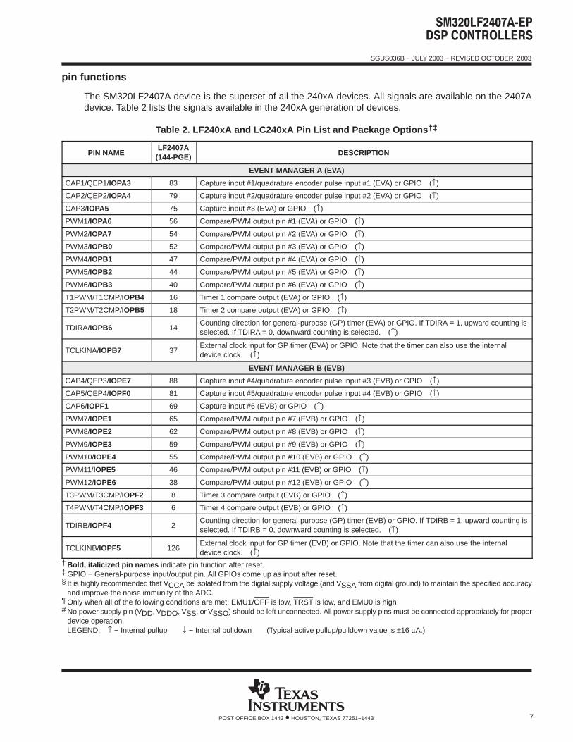
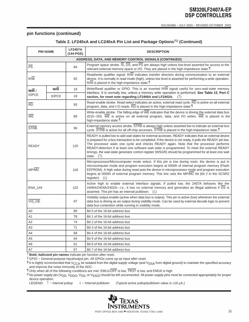
The SM320LF2407A device is the superset of all the 240xA devices. All signals are available on the 2407Adevice. Table 2 lists the signals available in the 240xA generation of devices.
Table 2. LF240xA and LC240xA Pin List and Package Options †‡
PIN NAMELF2407A
(144-PGE) DESCRIPTION
EVENT MANAGER A (EVA)
CAP1/QEP1/IOPA3 83 Capture input #1/quadrature encoder pulse input #1 (EVA) or GPIO (↑)
CAP2/QEP2/IOPA4 79 Capture input #2/quadrature encoder pulse input #2 (EVA) or GPIO (↑)
CAP3/IOPA5 75 Capture input #3 (EVA) or GPIO (↑)
PWM1/IOPA6 56 Compare/PWM output pin #1 (EVA) or GPIO (↑)
PWM2/IOPA7 54 Compare/PWM output pin #2 (EVA) or GPIO (↑)
PWM3/IOPB0 52 Compare/PWM output pin #3 (EVA) or GPIO (↑)
PWM4/IOPB1 47 Compare/PWM output pin #4 (EVA) or GPIO (↑)
PWM5/IOPB2 44 Compare/PWM output pin #5 (EVA) or GPIO (↑)
PWM6/IOPB3 40 Compare/PWM output pin #6 (EVA) or GPIO (↑)
T1PWM/T1CMP/IOPB4 16 Timer 1 compare output (EVA) or GPIO (↑)
T2PWM/T2CMP/IOPB5 18 Timer 2 compare output (EVA) or GPIO (↑)
TDIRA/IOPB6 14Counting direction for general-purpose (GP) timer (EVA) or GPIO. If TDIRA = 1, upward counting isselected. If TDIRA = 0, downward counting is selected. (↑)
TCLKINA/IOPB7 37External clock input for GP timer (EVA) or GPIO. Note that the timer can also use the internaldevice clock. (↑)
EVENT MANAGER B (EVB)
CAP4/QEP3/IOPE7 88 Capture input #4/quadrature encoder pulse input #3 (EVB) or GPIO (↑)
CAP5/QEP4/IOPF0 81 Capture input #5/quadrature encoder pulse input #4 (EVB) or GPIO (↑)
CAP6/IOPF1 69 Capture input #6 (EVB) or GPIO (↑)
PWM7/IOPE1 65 Compare/PWM output pin #7 (EVB) or GPIO (↑)
PWM8/IOPE2 62 Compare/PWM output pin #8 (EVB) or GPIO (↑)
PWM9/IOPE3 59 Compare/PWM output pin #9 (EVB) or GPIO (↑)
PWM10/IOPE4 55 Compare/PWM output pin #10 (EVB) or GPIO (↑)
PWM11/IOPE5 46 Compare/PWM output pin #11 (EVB) or GPIO (↑)
PWM12/IOPE6 38 Compare/PWM output pin #12 (EVB) or GPIO (↑)
T3PWM/T3CMP/IOPF2 8 Timer 3 compare output (EVB) or GPIO (↑)
T4PWM/T4CMP/IOPF3 6 Timer 4 compare output (EVB) or GPIO (↑)
TDIRB/IOPF4 2Counting direction for general-purpose (GP) timer (EVB) or GPIO. If TDIRB = 1, upward counting isselected. If TDIRB = 0, downward counting is selected. (↑)
TCLKINB/IOPF5 126External clock input for GP timer (EVB) or GPIO. Note that the timer can also use the internaldevice clock. (↑)
† Bold, italicized pin names indicate pin function after reset.‡ GPIO − General-purpose input/output pin. All GPIOs come up as input after reset.§ It is highly recommended that VCCA be isolated from the digital supply voltage (and VSSA from digital ground) to maintain the specified accuracy
and improve the noise immunity of the ADC.¶ Only when all of the following conditions are met: EMU1/OFF is low, TRST is low, and EMU0 is high# No power supply pin (VDD, VDDO, VSS, or VSSO) should be left unconnected. All power supply pins must be connected appropriately for proper
device operation.LEGEND: ↑ − Internal pullup ↓ − Internal pulldown (Typical active pullup/pulldown value is ±16 µA.)
SGUS036B − JULY 2003 − REVISED OCTOBER 2003
8 POST OFFICE BOX 1443 • HOUSTON, TEXAS 77251−1443
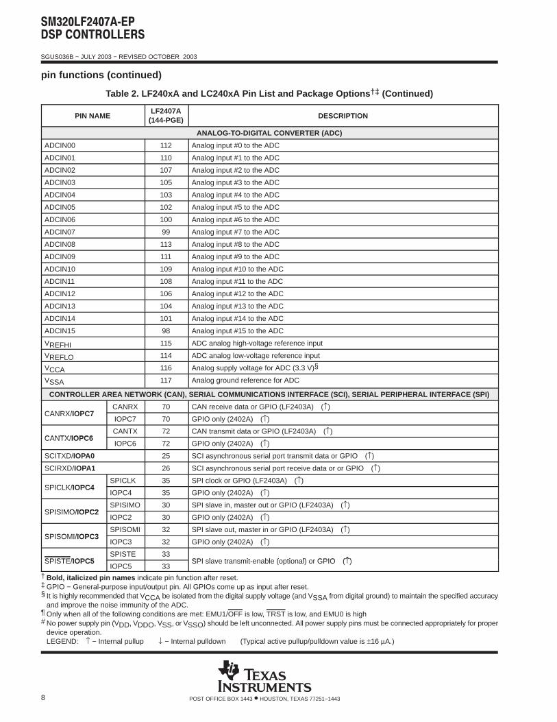
pin functions (continued)
Table 2. LF240xA and LC240xA Pin List and Package Options †‡ (Continued)
PIN NAMELF2407A
(144-PGE) DESCRIPTION
ANALOG-TO-DIGITAL CONVERTER (ADC)
ADCIN00 112 Analog input #0 to the ADC
ADCIN01 110 Analog input #1 to the ADC
ADCIN02 107 Analog input #2 to the ADC
ADCIN03 105 Analog input #3 to the ADC
ADCIN04 103 Analog input #4 to the ADC
ADCIN05 102 Analog input #5 to the ADC
ADCIN06 100 Analog input #6 to the ADC
ADCIN07 99 Analog input #7 to the ADC
ADCIN08 113 Analog input #8 to the ADC
ADCIN09 111 Analog input #9 to the ADC
ADCIN10 109 Analog input #10 to the ADC
ADCIN11 108 Analog input #11 to the ADC
ADCIN12 106 Analog input #12 to the ADC
ADCIN13 104 Analog input #13 to the ADC
ADCIN14 101 Analog input #14 to the ADC
ADCIN15 98 Analog input #15 to the ADC
VREFHI 115 ADC analog high-voltage reference input
VREFLO 114 ADC analog low-voltage reference input
VCCA 116 Analog supply voltage for ADC (3.3 V)§
VSSA 117 Analog ground reference for ADC
CONTROLLER AREA NETWORK (CAN), SERIAL COMMUNICATIONS INTERFACE (SCI), SERIAL PERIPHERAL INTERFACE (SPI)
CANRX/IOPC7CANRX 70 CAN receive data or GPIO (LF2403A) (↑)
CANRX/IOPC7IOPC7 70 GPIO only (2402A) (↑)
CANTX/IOPC6CANTX 72 CAN transmit data or GPIO (LF2403A) (↑)
CANTX/IOPC6IOPC6 72 GPIO only (2402A) (↑)
SCITXD/IOPA0 25 SCI asynchronous serial port transmit data or GPIO (↑)
SCIRXD/IOPA1 26 SCI asynchronous serial port receive data or or GPIO (↑)
SPICLK/IOPC4SPICLK 35 SPI clock or GPIO (LF2403A) (↑)
SPICLK/IOPC4IOPC4 35 GPIO only (2402A) (↑)
SPISIMO/IOPC2SPISIMO 30 SPI slave in, master out or GPIO (LF2403A) (↑)
SPISIMO/IOPC2IOPC2 30 GPIO only (2402A) (↑)
SPISOMI/IOPC3SPISOMI 32 SPI slave out, master in or GPIO (LF2403A) (↑)
SPISOMI/IOPC3IOPC3 32 GPIO only (2402A) (↑)
SPISTE/IOPC5SPISTE 33
SPI slave transmit-enable (optional) or GPIO (↑)SPISTE/IOPC5IOPC5 33
SPI slave transmit-enable (optional) or GPIO (↑)
† Bold, italicized pin names indicate pin function after reset.‡ GPIO − General-purpose input/output pin. All GPIOs come up as input after reset.§ It is highly recommended that VCCA be isolated from the digital supply voltage (and VSSA from digital ground) to maintain the specified accuracy
and improve the noise immunity of the ADC.¶ Only when all of the following conditions are met: EMU1/OFF is low, TRST is low, and EMU0 is high# No power supply pin (VDD, VDDO, VSS, or VSSO) should be left unconnected. All power supply pins must be connected appropriately for proper
device operation.LEGEND: ↑ − Internal pullup ↓ − Internal pulldown (Typical active pullup/pulldown value is ±16 µA.)
SGUS036B − JULY 2003 − REVISED OCTOBER 2003
9POST OFFICE BOX 1443 • HOUSTON, TEXAS 77251−1443
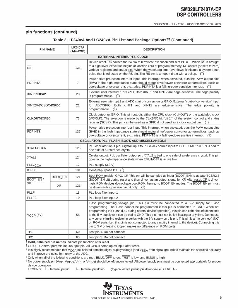
pin functions (continued)
Table 2. LF240xA and LC240xA Pin List and Package Options †‡ (Continued)
PIN NAMELF2407A
(144-PGE) DESCRIPTION
EXTERNAL INTERRUPTS, CLOCK
RS 133
Device reset. RS causes the 240xA to terminate execution and sets PC = 0. When RS is broughtto a high level, execution begins at location zero of program memory. RS affects (or sets to zero)various registers and status bits. When the watchdog timer overflows, it initiates a system resetpulse that is reflected on the RS pin. The RS pin is an open drain with a pullup. (↑)
PDPINTA 7Power drive protection interrupt input. This interrupt, when activated, puts the PWM output pins(EVA) in the high-impedance state should motor drive/power converter abnormalities, such asovervoltage or overcurrent, etc., arise. PDPINTA is a falling-edge-sensitive interrupt. (↑)
XINT1/IOPA2 23External user interrupt 1 or GPIO. Both XINT1 and XINT2 are edge-sensitive. The edge polarityis programmable. (↑)
XINT2/ADCSOC/IOPD0 21External user interrupt 2 and ADC start of conversion or GPIO. External “start-of-conversion” inputfor ADC/GPIO. Both XINT1 and XINT2 are edge-sensitive. The edge polarity isprogrammable. (↑)
CLKOUT /IOPE0 73Clock output or GPIO. This pin outputs either the CPU clock (CLKOUT) or the watchdog clock(WDCLK). The selection is made by the CLKSRC bit (bit 14) of the system control and statusregister (SCSR). This pin can be used as a GPIO if not used as a clock output pin. (↑)
PDPINTB 137Power drive protection interrupt input. This interrupt, when activated, puts the PWM output pins(EVB) in the high-impedance state should motor drive/power converter abnormalities, such asovervoltage or overcurrent, etc., arise. PDPINTB is a falling-edge-sensitive interrupt. (↑)
OSCILLATOR, PLL, FLASH, BOOT, AND MISCELLANEOUS
XTAL1/CLKIN 123PLL oscillator input pin. Crystal input to PLL/clock source input to PLL. XTAL1/CLKIN is tied toone side of a reference crystal.
XTAL2 124Crystal output. PLL oscillator output pin. XTAL2 is tied to one side of a reference crystal. This pingoes in the high-impedance state when EMU1/OFF is active low.
PLLVCCA 12 PLL supply (3.3 V)
IOPF6 131 General-purpose I/O (↑)
BOOT_EN /BOOT_EN 121 Boot ROM enable, GPO, XF. This pin will be sampled as input (BOOT_EN) to update SCSR2.3
(BOOT_EN bit) during reset and then driven as an output signal for XF. After reset, XF is drivenBOOT_EN /XF
XF 121
(BOOT_EN bit) during reset and then driven as an output signal for XF. After reset, XF is drivenhigh. ROM devices do not have boot ROM, hence, no BOOT_EN modes. The BOOT_EN pin mustbe driven with a passive circuit only. (↑)
PLLF 11 PLL loop filter input 1
PLLF2 10 PLL loop filter input 2
VCCP (5V) 58
Flash programming voltage pin. This pin must be connected to a 5-V supply for Flashprogramming. The Flash cannot be programmed if this pin is connected to GND. When notprogramming the Flash (i.e., during normal device operation), this pin can either be left connectedto the 5-V supply or it can be tied to GND. This pin must not be left floating at any time. Do not useany current-limiting resistor in series with the 5-V supply on this pin. This pin is a “no connect” (NC)on ROM parts (i.e., this pin is not connected to any circuitry internal to the device). Connecting thispin to 5 V or leaving it open makes no difference on ROM parts.
TP1 60 Test pin 1. Do not connect.
TP2 63 Test pin 2. Do not connect.† Bold, italicized pin names indicate pin function after reset.‡ GPIO − General-purpose input/output pin. All GPIOs come up as input after reset.§ It is highly recommended that VCCA be isolated from the digital supply voltage (and VSSA from digital ground) to maintain the specified accuracy
and improve the noise immunity of the ADC.¶ Only when all of the following conditions are met: EMU1/OFF is low, TRST is low, and EMU0 is high# No power supply pin (VDD, VDDO, VSS, or VSSO) should be left unconnected. All power supply pins must be connected appropriately for proper
device operation.LEGEND: ↑ − Internal pullup ↓ − Internal pulldown (Typical active pullup/pulldown value is ±16 µA.)
SGUS036B − JULY 2003 − REVISED OCTOBER 2003
10 POST OFFICE BOX 1443 • HOUSTON, TEXAS 77251−1443
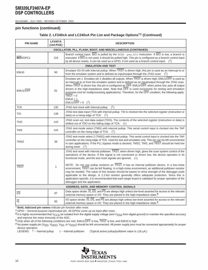
pin functions (continued)
Table 2. LF240xA and LC240xA Pin List and Package Options †‡ (Continued)
PIN NAMELF2407A
(144-PGE) DESCRIPTION
OSCILLATOR, PLL, FLASH, BOOT, AND MISCELLANEOUS (CONTINUED)
BIO/IOPC1 119Branch control input. BIO is polled by the BCND pma,BIO instruction. If BIO is low, a branch isexecuted. If BIO is not used, it should be pulled high. This pin is configured as a branch control inputby all device resets. It can be used as a GPIO, if not used as a branch control input. (↑)
EMULATION AND TEST
EMU0 90Emulator I/O #0 with internal pullup. When TRST is driven high, this pin is used as an interrupt to orfrom the emulator system and is defined as input/output through the JTAG scan. (↑)
EMU1/OFF 91
Emulator pin 1. Emulator pin 1 disables all outputs. When TRST is driven high, EMU1/OFF is used asan interrupt to or from the emulator system and is defined as an input/output through the JTAG scan.When TRST is driven low, this pin is configured as OFF. EMU1/OFF, when active low, puts all outputdrivers in the high-impedance state. Note that OFF is used exclusively for testing and emulationpurposes (not for multiprocessing applications). Therefore, for the OFF condition, the following apply:TRST = 0EMU0 = 1EMU1/OFF = 0 (↑)
TCK 135 JTAG test clock with internal pullup (↑)
TDI 139JTAG test data input (TDI) with internal pullup. TDI is clocked into the selected register (instruction ordata) on a rising edge of TCK. (↑)
TDO 142JTAG scan out, test data output (TDO). The contents of the selected register (instruction or data) isshifted out of TDO on the falling edge of TCK. (↓)
TMS 144JTAG test-mode select (TMS) with internal pullup. This serial control input is clocked into the TAPcontroller on the rising edge of TCK. (↑)
TMS2 36
JTAG test-mode select 2 (TMS2) with internal pullup. This serial control input is clocked into the TAPcontroller on the rising edge of TCK. Used for test and emulation only. This pin can be left unconnectedin user applications. If the PLL bypass mode is desired, TMS2, TMS, and TRST should be held lowduring reset. (↑)
TRST 1
JTAG test reset with internal pulldown. TRST, when driven high, gives the scan system control of theoperations of the device. If this signal is not connected or driven low, the device operates in itsfunctional mode, and the test reset signals are ignored. (↓)
NOTE: Do not use pullup resistors on TRST; it has an internal pulldown device. In a low-noiseenvironment, TRST can be left floating. In a high-noise environment, an additional pulldown resistormay be needed. The value of this resistor should be based on drive strength of the debugger podsapplicable to the design. A 2.2-kΩ resistor generally offers adequate protection. Since this isapplication-specific, it is recommended that each target board is validated for proper operation of thedebugger and the application.
ADDRESS, DATA, AND MEMORY CONTROL SIGNALS
DS 87Data space strobe. IS, DS, and PS are always high unless low-level asserted for access to the relevantexternal memory space or I/O. They are placed in the high-impedance state.¶
IS 82I/O space strobe. IS, DS, and PS are always high unless low-level asserted for access to the relevantexternal memory space or I/O. They are placed in the high-impedance state.¶
† Bold, italicized pin names indicate pin function after reset.‡ GPIO − General-purpose input/output pin. All GPIOs come up as input after reset.§ It is highly recommended that VCCA be isolated from the digital supply voltage (and VSSA from digital ground) to maintain the specified accuracy
and improve the noise immunity of the ADC.¶ Only when all of the following conditions are met: EMU1/OFF is low, TRST is low, and EMU0 is high# No power supply pin (VDD, VDDO, VSS, or VSSO) should be left unconnected. All power supply pins must be connected appropriately for proper
device operation.LEGEND: ↑ − Internal pullup ↓ − Internal pulldown (Typical active pullup/pulldown value is ±16 µA.)
SGUS036B − JULY 2003 − REVISED OCTOBER 2003
11POST OFFICE BOX 1443 • HOUSTON, TEXAS 77251−1443
pin functions (continued)
Table 2. LF240xA and LC240xA Pin List and Package Options †‡ (Continued)
PIN NAMELF2407A
(144-PGE) DESCRIPTION
ADDRESS, DATA, AND MEMORY CONTROL SIGNALS (CONTINUED)
PS 84Program space strobe. IS, DS, and PS are always high unless low-level asserted for access to therelevant external memory space or I/O. They are placed in the high-impedance state.¶
R/W 92Read/write qualifier signal. R/W indicates transfer direction during communication to an externaldevice. It is normally in read mode (high), unless low level is asserted for performing a write operation.R/W is placed in the high-impedance state.¶
W/R / W/R 19 Write/Read qualifier or GPIO. This is an inverted R/W signal useful for zero-wait-state memoryinterface. It is normally low, unless a memory write operation is performed. See Table 12, Port C
W/R /IOPC0 IOPC0 19
interface. It is normally low, unless a memory write operation is performed. See Table 12, Port Csection, for reset note regarding LF2406A and LF2402A. (↑)
RD 93Read-enable strobe. Read-select indicates an active, external read cycle. RD is active on all externalprogram, data, and I /O reads. RD is placed in the high-impedance state.¶
WE 89Write-enable strobe. The falling edge of WE indicates that the device is driving the external data bus(D15−D0). WE is active on all external program, data, and I/O writes. WE is placed in thehigh-impedance state.¶
STRB 96External memory access strobe. STRB is always high unless asserted low to indicate an external buscycle. STRB is active for all off-chip accesses. STRB is placed in the high-impedance state.¶
READY 120
READY is pulled low to add wait states for external accesses. READY indicates that an external deviceis prepared for a bus transaction to be completed. If the device is not ready, it pulls the READY pin low.The processor waits one cycle and checks READY again. Note that the processor performsREADY-detection if at least one software wait state is programmed. To meet the external READYtimings, the wait-state generator control register (WSGR) should be programmed for at least one waitstate. (↑)
MP/MC 118
Microprocessor/Microcomputer mode select. If this pin is low during reset, the device is put inmicrocomputer mode and program execution begins at 0000h of internal program memory (FlashEEPROM). A high value during reset puts the device in microprocessor mode and program executionbegins at 0000h of external program memory. This line sets the MP/MC bit (bit 2 in the SCSR2register). (↓)
ENA_144 122Active high to enable external interface signals. If pulled low, the 2407A behaves like the2406A/2403A/2402A—i.e., it has no external memory and generates an illegal address if DS isasserted. This pin has an internal pulldown. (↓)
VIS_OE 97Visibility output enable (active when data bus is output). This pin is active (low) whenever the externaldata bus is driving as an output during visibility mode. Can be used by external decode logic to preventdata bus contention while running in visibility mode.
A0 80 Bit 0 of the 16-bit address bus
A1 78 Bit 1 of the 16-bit address bus
A2 74 Bit 2 of the 16-bit address bus
A3 71 Bit 3 of the 16-bit address bus
A4 68 Bit 4 of the 16-bit address bus
A5 64 Bit 5 of the 16-bit address bus
A6 61 Bit 6 of the 16-bit address bus
A7 57 Bit 7 of the 16-bit address bus† Bold, italicized pin names indicate pin function after reset.‡ GPIO − General-purpose input/output pin. All GPIOs come up as input after reset.§ It is highly recommended that VCCA be isolated from the digital supply voltage (and VSSA from digital ground) to maintain the specified accuracy
and improve the noise immunity of the ADC.¶ Only when all of the following conditions are met: EMU1/OFF is low, TRST is low, and EMU0 is high# No power supply pin (VDD, VDDO, VSS, or VSSO) should be left unconnected. All power supply pins must be connected appropriately for proper
device operation.LEGEND: ↑ − Internal pullup ↓ − Internal pulldown (Typical active pullup/pulldown value is ±16 µA.)
SGUS036B − JULY 2003 − REVISED OCTOBER 2003
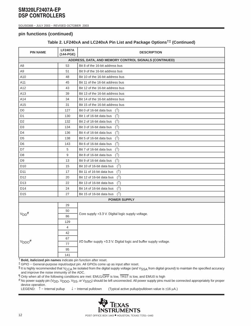
12 POST OFFICE BOX 1443 • HOUSTON, TEXAS 77251−1443
pin functions (continued)
Table 2. LF240xA and LC240xA Pin List and Package Options †‡ (Continued)
PIN NAMELF2407A
(144-PGE) DESCRIPTION
ADDRESS, DATA, AND MEMORY CONTROL SIGNALS (CONTINUED)
A8 53 Bit 8 of the 16-bit address bus
A9 51 Bit 9 of the 16-bit address bus
A10 48 Bit 10 of the 16-bit address bus
A11 45 Bit 11 of the 16-bit address bus
A12 43 Bit 12 of the 16-bit address bus
A13 39 Bit 13 of the 16-bit address bus
A14 34 Bit 14 of the 16-bit address bus
A15 31 Bit 15 of the 16-bit address bus
D0 127 Bit 0 of 16-bit data bus (↑)
D1 130 Bit 1 of 16-bit data bus (↑)
D2 132 Bit 2 of 16-bit data bus (↑)
D3 134 Bit 3 of 16-bit data bus (↑)
D4 136 Bit 4 of 16-bit data bus (↑)
D5 138 Bit 5 of 16-bit data bus (↑)
D6 143 Bit 6 of 16-bit data bus (↑)
D7 5 Bit 7 of 16-bit data bus (↑)
D8 9 Bit 8 of 16-bit data bus (↑)
D9 13 Bit 9 of 16-bit data bus (↑)
D10 15 Bit 10 of 16-bit data bus (↑)
D11 17 Bit 11 of 16-bit data bus (↑)
D12 20 Bit 12 of 16-bit data bus (↑)
D13 22 Bit 13 of 16-bit data bus (↑)
D14 24 Bit 14 of 16-bit data bus (↑)
D15 27 Bit 15 of 16-bit data bus (↑)
POWER SUPPLY
29
VDD#50
Core supply +3.3 V. Digital logic supply voltage.VDD#86
Core supply +3.3 V. Digital logic supply voltage.
129
4
42
VDDO#67
I/O buffer supply +3.3 V. Digital logic and buffer supply voltage.VDDO#77
I/O buffer supply +3.3 V. Digital logic and buffer supply voltage.
95
141† Bold, italicized pin names indicate pin function after reset.‡ GPIO − General-purpose input/output pin. All GPIOs come up as input after reset.§ It is highly recommended that VCCA be isolated from the digital supply voltage (and VSSA from digital ground) to maintain the specified accuracy
and improve the noise immunity of the ADC.¶ Only when all of the following conditions are met: EMU1/OFF is low, TRST is low, and EMU0 is high# No power supply pin (VDD, VDDO, VSS, or VSSO) should be left unconnected. All power supply pins must be connected appropriately for proper
device operation.LEGEND: ↑ − Internal pullup ↓ − Internal pulldown (Typical active pullup/pulldown value is ±16 µA.)
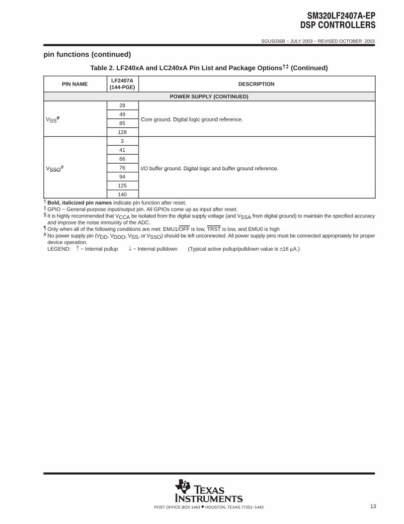
SGUS036B − JULY 2003 − REVISED OCTOBER 2003
13POST OFFICE BOX 1443 • HOUSTON, TEXAS 77251−1443
pin functions (continued)
Table 2. LF240xA and LC240xA Pin List and Package Options †‡ (Continued)
PIN NAMELF2407A
(144-PGE) DESCRIPTION
POWER SUPPLY (CONTINUED)
28
VSS#49
Core ground. Digital logic ground reference.VSS#85
Core ground. Digital logic ground reference.
128
3
41
66
VSSO# 76 I/O buffer ground. Digital logic and buffer ground reference.VSSO#
94
I/O buffer ground. Digital logic and buffer ground reference.
125
140† Bold, italicized pin names indicate pin function after reset.‡ GPIO − General-purpose input/output pin. All GPIOs come up as input after reset.§ It is highly recommended that VCCA be isolated from the digital supply voltage (and VSSA from digital ground) to maintain the specified accuracy
and improve the noise immunity of the ADC.¶ Only when all of the following conditions are met: EMU1/OFF is low, TRST is low, and EMU0 is high# No power supply pin (VDD, VDDO, VSS, or VSSO) should be left unconnected. All power supply pins must be connected appropriately for proper
device operation.LEGEND: ↑ − Internal pullup ↓ − Internal pulldown (Typical active pullup/pulldown value is ±16 µA.)
SGUS036B − JULY 2003 − REVISED OCTOBER 2003
14 POST OFFICE BOX 1443 • HOUSTON, TEXAS 77251−1443
memory maps
ÈÈÈÈÈÈÈÈÈÈÈÈÈÈÈÈÈÈÈÈÈÈÈÈÈÈÈÈÈÈ
ÈÈÈÈÈÈÈÈÈÈÈÈÈÈÈÈÈÈÈÈ
ÈÈÈÈÈÈÈÈÈÈÈÈÈÈÈÈÈÈÈÈÈÈÈÈÈÈÈÈÈÈ
ÈÈÈÈÈÈÈÈÈÈÈÈÈÈÈÈÈÈÈÈÈÈÈÈÈÈÈÈÈÈ
ÈÈÈÈÈÈÈÈÈÈÈÈÈÈÈÈÈÈÈÈÈÈÈÈÈÈÈÈÈÈÈÈÈÈÈÈÈÈÈÈ
ÉÉÉÉÉÉÉÉÉÉÉÉÉÉÉÉÉÉÉÉÉÉÉÉÉÉÉÉÉÉ
Reserved
0000Hex Program
On-Chip Flash Memory (Sectored) − if MP/MC = 0External Program Memory − if MP/MC = 1
7FFF8000
0000
005F0060
Hex Data
Memory-MappedRegisters/Reserved Addresses
007F0080
On-Chip DARAM B2
01FF
Illegal
02FF0300
On-Chip DARAM (B0)§ (CNF = 0)Reserved (CNF = 1)
ÈÈÈÈÈÈÈÈÈÈÈÈÈÈÈÈÈÈÈÈÈÈÈÈÈÈÈÈÈÈ
03FF0400
On-Chip DARAM (B1) ¶
07FF0800
Reserved
6FFF7000
Illegal
Peripheral Memory-MappedRegisters (System, WD, ADC,SCI, SPI, CAN, I/O, Interrupts)7FFF
8000
External
0000Hex I/O
FEFFFF00
FF0E
FF0F
Reserved
External
FFFF
FEFFFF00
FDFFFE00
External
On-Chip DARAM (B0) ‡ (CNF = 1) External (CNF = 0)
FFFF
FFFE
Wait-State Generator ControlRegister (On-Chip)
FF10
Flash Control Mode Register
SARAM (See Table 1 for details.)
FFFF
SARAM (2K)Internal (PON = 1)External (PON=0)
87FF8800
0FFF1000
3FFF
Flash Sector 1 (12K)
Flash Sector 2 (12K)
Flash Sector 3 (4K)
4000
6FFF7000
0FFF1000
0200
ÉÉÉÉÉÉÉÉÉÉÉÉÉÉÉÉÉÉÉÉÉÉÉÉÉÉÉÉÉÉ
SARAM (2K)Internal (DON = 1)Reserved (DON=0)
ÉÉÉÉÉÉÈÈÈÈÈÈ
Reserved or Illegal
Flash Sector 0 (4K)
Interrupt Vectors (0000−003Fh)Reserved† (0040−0043h)User code begins at 0044h
Reserved ‡ (CNF = 1)External (CNF = 0)
Reserved
00FF0100
Illegal04FF0500
NOTE A: Boot ROM: If the boot ROM is enabled, then addresses 0000−00FF in the program space will be occupied by boot ROM.† Addresses 0040h−0043h in on-chip program memory are reserved for code security passwords.‡ When CNF = 1, addresses FE00h−FEFFh and FF00h−FFFFh are mapped to the same physical block (B0) in program-memory space. For
example, a write to FE00h has the same effect as a write to FF00h. For simplicity, addresses FE00h−FEFFh are referred to as reserved whenCNF = 1.
§ When CNF = 0, addresses 0100h−01FFh and 0200h−02FFh are mapped to the same physical block (B0) in data-memory space. For example,a write to 0100h has the same effect as a write to 0200h. For simplicity, addresses 0100h−01FFh are referred to as reserved.
¶ Addresses 0300h−03FFh and 0400h−04FFh are mapped to the same physical block (B1) in data-memory space. For example, a write to 0400hhas the same effect as a write to 0300h. For simplicity, addresses 0400h−04FFh are referred to as reserved.
Figure 1. SM320LF2407A Memory Map
SGUS036B − JULY 2003 − REVISED OCTOBER 2003
15POST OFFICE BOX 1443 • HOUSTON, TEXAS 77251−1443
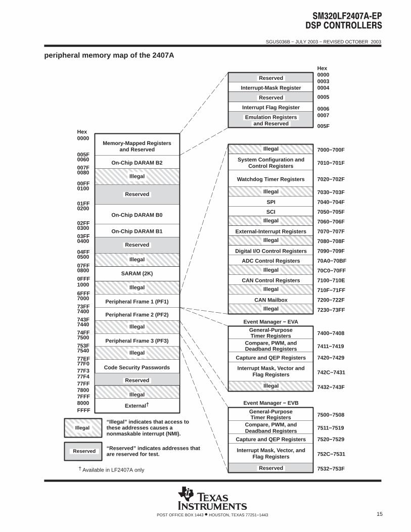
peripheral memory map of the 2407A
ÈÈÈÈÈÈÈÈÈÈÈÈÈÈÈÈÈÈ
ÈÈÈÈÈÈÈÈÈÈÈÈÈÈÈÈÈÈ
ÈÈÈÈÈÈÈÈÈÈÈÈÈÈÈÈÈÈ
ÈÈÈÈÈÈÈÈÈÈÈÈÈÈÈÈÈÈ
ÈÈÈÈÈÈÈÈÈÈÈÈÈÈÈÈÈÈ
ÈÈÈÈÈÈÈÈÈÈÈÈÈÈÈÈÈÈ
ÈÈÈÈÈÈÈÈÈÈÈÈÈÈÈÈÈÈ
ÈÈÈÈÈÈÈÈÈÈÈÈÈÈÈÈÈÈ
ÈÈÈÈÈÈÈÈÈÈÈÈÈÈÈÈÈÈ
Reserved
Reserved
ÈÈÈÈÈÈÈÈÈÈÈÈÈÈÈÈÈÈ
ÈÈÈÈÈÈÈÈÈÈÈÈÈÈÈÈÈÈ
70C0−70FF
General-PurposeTimer Registers
Flag Registers
Event Manager − EVB
Deadband RegistersCompare, PWM, and
Interrupt Mask, Vector, and
Capture and QEP Registers
7500−7508
7511−7519
7520−7529
752C−7531
7532−753F
7432−743F
742C−7431
7420−7429
7411−7419
7400−7408
Illegal
Flag RegistersInterrupt Mask, Vector and
Capture and QEP Registers
Deadband RegistersCompare, PWM, and
Timer RegistersGeneral-Purpose
Event Manager − EVA
710F−71FF
7100−710E
70A0−70BF
7090−709F
7080−708F
7070−707F
7060−706F
7050−705F
7040−704F
7030−703F
7020−702F
7010−701F
7000−700F
CAN Control Registers
ADC Control Registers
Digital I/O Control Registers
External-Interrupt Registers
SCI
SPI
Watchdog Timer Registers
Control RegistersSystem Configuration and
Hex
Hex005F
00070006
0005
000400030000
and ReservedEmulation Registers
Interrupt Flag Register
Interrupt-Mask Register
FFFF
77F077EF
7540753F
750074FF
7440743F
740073FF
70006FFF
1000
07FF
040003FF
030002FF
020001FF
0080007F
0060005F
0000
External †
Peripheral Frame 3 (PF3)
Peripheral Frame 2 (PF2)
Peripheral Frame 1 (PF1)
On-Chip DARAM B1
On-Chip DARAM B0
Reserved
On-Chip DARAM B2
and ReservedMemory-Mapped Registers
“Illegal” indicates that access tothese addresses causes anonmaskable interrupt (NMI).
ÈÈÈÈÈÈÈÈÈÈÈÈ
Reserved “Reserved” indicates addresses thatare reserved for test.
† Available in LF2407A only
ÈÈÈÈÈÈÈÈÈÈÈÈÈÈÈÈÈÈ
Illegal
Illegal
Illegal
Illegal
Illegal
Illegal
Illegal
Illegal
Illegal
Illegal
010000FF
Reserved
ÈÈÈÈÈÈÈÈÈÈÈÈÈÈÈÈÈÈ
Illegal050004FF
SARAM (2K)0800
0FFF
ÈÈÈÈÈÈÈÈÈÈÈÈÈÈÈÈÈÈ
CAN Mailbox
Illegal 7230−73FF
7200−722F
Illegal
Reserved
Code Security Passwords
Illegal
77F377F4
7FFF8000
Reserved77FF7800
SGUS036B − JULY 2003 − REVISED OCTOBER 2003
16 POST OFFICE BOX 1443 • HOUSTON, TEXAS 77251−1443
device reset and interrupts
The 240xA software-programmable interrupt structure supports flexible on-chip and external interruptconfigurations to meet real-time interrupt-driven application requirements. The LF240xA recognizes three typesof interrupt sources.
Reset (hardware- or software-initiated) is unarbitrated by the CPU and takes immediate priority over anyother executing functions. All maskable interrupts are disabled until the reset service routine enables them.
The LF240xA devices have two sources of reset: an external reset pin and a watchdog timer time-out(reset).
Hardware-generated interrupts are requested by external pins or by on-chip peripherals. There are twotypes:
− External interrupts are generated by one of four external pins corresponding to the interrupts XINT1,XINT2, PDPINTA, and PDPINTB. These four can be masked both by dedicated enable bits and by theCPU’s interrupt mask register (IMR), which can mask each maskable interrupt line at the DSP core.
− Peripheral interrupts are initiated internally by these on-chip peripheral modules: event manager A,event manager B, SPI, SCI, CAN, and ADC. They can be masked both by enable bits for each event ineach peripheral and by the CPU’s IMR, which can mask each maskable interrupt line at the DSP core.
Software-generated interrupts for the LF240xA devices include:
− The INTR instruction. This instruction allows initialization of any LF240xA interrupt with software. Itsoperand indicates the interrupt vector location to which the CPU branches. This instruction globallydisables maskable interrupts (sets the INTM bit to 1).
− The NMI instruction. This instruction forces a branch to interrupt vector location 24h. This instructionglobally disables maskable interrupts. 240xA devices do not have the NMI hardware signal, onlysoftware activation is provided.
− The TRAP instruction. This instruction forces the CPU to branch to interrupt vector location 22h. TheTRAP instruction does not disable maskable interrupts (INTM is not set to 1); therefore, when the CPUbranches to the interrupt service routine, that routine can be interrupted by the maskable hardwareinterrupts.
− An emulator trap. This interrupt can be generated with either an INTR instruction or a TRAP instruction.
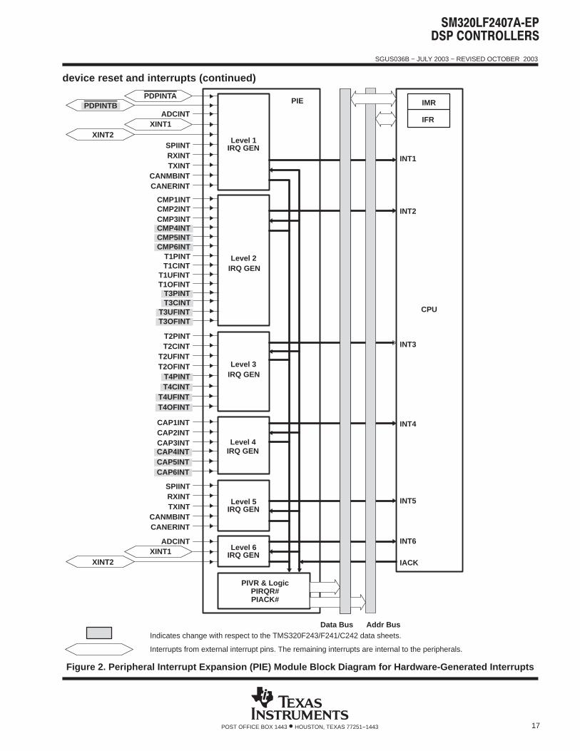
Six core interrupts (INT1−INT6) are expanded using a peripheral interrupt expansion (PIE) module identical tothe F24x devices. The PIE manages all the peripheral interrupts from the 240xA peripherals and are grouped toshare the six core level interrupts. Figure 2 shows the PIE block diagram for hardware-generated interrupts.
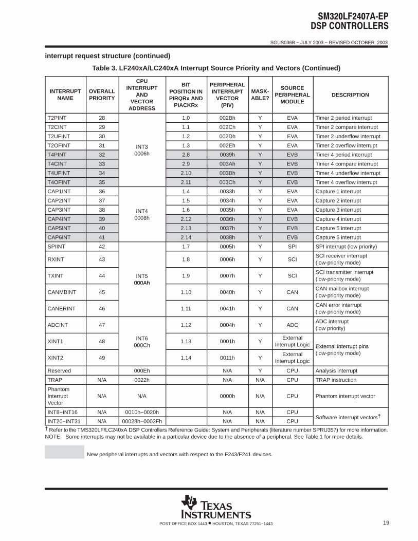
The PIE block diagram (Figure 2) and the interrupt table (Table 3) explain the grouping and interrupt vectormaps. LF240xA devices have interrupts identical to those of the F24x devices and should be completelycode-compatible. 240xA devices also have peripheral interrupts identical to those of the F24x − plus additionalinterrupts for new peripherals such as event manager B. Though the new interrupts share the 24x interruptgrouping, they all have a unique vector to differentiate among the interrupts. See Table 3 for details.
SGUS036B − JULY 2003 − REVISED OCTOBER 2003
17POST OFFICE BOX 1443 • HOUSTON, TEXAS 77251−1443
device reset and interrupts (continued)
CPU
IACK
Addr BusData Bus
PIVR & LogicPIRQR#PIACK#
IRQ GENLevel 6
IRQ GENLevel 5
IRQ GENLevel 4
IRQ GENLevel 3
IRQ GENLevel 2
IRQ GENLevel 1
ADCINT
CANERINTCANMBINT
TXINTRXINTSPIINT
CAP3INTCAP2INTCAP1INT
T2OFINTT2UFINT
T2CINTT2PINT
T1OFINTT1UFINT
T1CINTT1PINT
CMP3INTCMP2INTCMP1INT
CANERINTCANMBINT
TXINTRXINTSPIINT
ADCINTPDPINTB
INT1
INT2
INT3
INT4
INT6
INT5
IMR
IFR
PIE
CAP6INTCAP5INTCAP4INT
T4OFINTT4UFINT
T4CINTT4PINT
CMP6INTCMP5INTCMP4INT
T3OFINTT3UFINT
T3PINTT3CINT
PDPINTA
Indicates change with respect to the TMS320F243/F241/C242 data sheets.
XINT1XINT2
XINT1XINT2
Interrupts from external interrupt pins. The remaining interrupts are internal to the peripherals.
Figure 2. Peripheral Interrupt Expansion (PIE) Module Block Diagram for Hardware-Generated Interrupts
SGUS036B − JULY 2003 − REVISED OCTOBER 2003
18 POST OFFICE BOX 1443 • HOUSTON, TEXAS 77251−1443
interrupt request structure
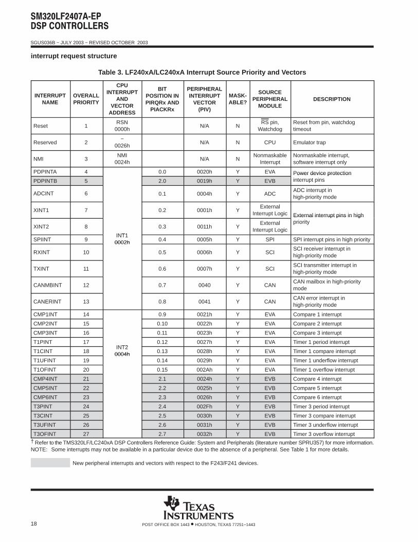
Table 3. LF240xA/LC240xA Interrupt Source Priority and Vectors
INTERRUPTNAME
OVERALLPRIORITY
CPUINTERRUPT
ANDVECTOR
ADDRESS
BITPOSITION INPIRQRx AND
PIACKRx
PERIPHERALINTERRUPT
VECTOR(PIV)
MASK-ABLE?
SOURCEPERIPHERAL
MODULEDESCRIPTION
Reset 1RSN
0000hN/A N
RS pin,Watchdog
Reset from pin, watchdogtimeout
Reserved 2−
0026hN/A N CPU Emulator trap
NMI 3NMI
0024hN/A N
NonmaskableInterrupt
Nonmaskable interrupt,software interrupt only
PDPINTA 4 0.0 0020h Y EVA Power device protection
PDPINTB 5 2.0 0019h Y EVB
Power device protectioninterrupt pins
ADCINT 6 0.1 0004h Y ADCADC interrupt inhigh-priority mode
XINT1 7 0.2 0001h YExternal
Interrupt Logic External interrupt pins in high
XINT2 8
INT1
0.3 0011h YExternal
Interrupt Logic
External interrupt pins in highpriority
SPIINT 9INT1
0002h 0.4 0005h Y SPI SPI interrupt pins in high priority
RXINT 10
0002h
0.5 0006h Y SCISCI receiver interrupt inhigh-priority mode
TXINT 11 0.6 0007h Y SCISCI transmitter interrupt inhigh-priority mode
CANMBINT 12 0.7 0040 Y CANCAN mailbox in high-prioritymode
CANERINT 13 0.8 0041 Y CANCAN error interrupt inhigh-priority mode
CMP1INT 14 0.9 0021h Y EVA Compare 1 interrupt
CMP2INT 15 0.10 0022h Y EVA Compare 2 interrupt
CMP3INT 16 0.11 0023h Y EVA Compare 3 interrupt
T1PINT 17INT2
0.12 0027h Y EVA Timer 1 period interrupt
T1CINT 18INT2
0004h 0.13 0028h Y EVA Timer 1 compare interrupt
T1UFINT 190004h
0.14 0029h Y EVA Timer 1 underflow interrupt
T1OFINT 20 0.15 002Ah Y EVA Timer 1 overflow interrupt
CMP4INT 21 2.1 0024h Y EVB Compare 4 interrupt
CMP5INT 22 2.2 0025h Y EVB Compare 5 interrupt
CMP6INT 23 2.3 0026h Y EVB Compare 6 interrupt
T3PINT 24 2.4 002Fh Y EVB Timer 3 period interrupt
T3CINT 25 2.5 0030h Y EVB Timer 3 compare interrupt
T3UFINT 26 2.6 0031h Y EVB Timer 3 underflow interrupt
T3OFINT 27 2.7 0032h Y EVB Timer 3 overflow interrupt† Refer to the TMS320LF/LC240xA DSP Controllers Reference Guide: System and Peripherals (literature number SPRU357) for more information.NOTE: Some interrupts may not be available in a particular device due to the absence of a peripheral. See Table 1 for more details.
New peripheral interrupts and vectors with respect to the F243/F241 devices.
SGUS036B − JULY 2003 − REVISED OCTOBER 2003
19POST OFFICE BOX 1443 • HOUSTON, TEXAS 77251−1443
interrupt request structure (continued)
Table 3. LF240xA/LC240xA Interrupt Source Priority and Vectors (Continued)
INTERRUPTNAME
OVERALLPRIORITY
CPUINTERRUPT
ANDVECTOR
ADDRESS
BITPOSITION INPIRQRx AND
PIACKRx
PERIPHERALINTERRUPT
VECTOR(PIV)
MASK-ABLE?
SOURCEPERIPHERAL
MODULEDESCRIPTION
T2PINT 28 1.0 002Bh Y EVA Timer 2 period interrupt
T2CINT 29 1.1 002Ch Y EVA Timer 2 compare interrupt
T2UFINT 30 1.2 002Dh Y EVA Timer 2 underflow interrupt
T2OFINT 31 INT3 1.3 002Eh Y EVA Timer 2 overflow interrupt
T4PINT 32
INT30006h 2.8 0039h Y EVB Timer 4 period interrupt
T4CINT 33
0006h
2.9 003Ah Y EVB Timer 4 compare interrupt
T4UFINT 34 2.10 003Bh Y EVB Timer 4 underflow interrupt
T4OFINT 35 2.11 003Ch Y EVB Timer 4 overflow interrupt
CAP1INT 36 1.4 0033h Y EVA Capture 1 interrupt
CAP2INT 37 1.5 0034h Y EVA Capture 2 interrupt
CAP3INT 38 INT4 1.6 0035h Y EVA Capture 3 interrupt
CAP4INT 39
INT40008h 2.12 0036h Y EVB Capture 4 interrupt
CAP5INT 40
0008h
2.13 0037h Y EVB Capture 5 interrupt
CAP6INT 41 2.14 0038h Y EVB Capture 6 interrupt
SPIINT 42 1.7 0005h Y SPI SPI interrupt (low priority)
RXINT 43 1.8 0006h Y SCISCI receiver interrupt (low-priority mode)
TXINT 44 INT5000Ah
1.9 0007h Y SCISCI transmitter interrupt(low-priority mode)
CANMBINT 45
000Ah
1.10 0040h Y CANCAN mailbox interrupt(low-priority mode)
CANERINT 46 1.11 0041h Y CANCAN error interrupt(low-priority mode)
ADCINT 47 1.12 0004h Y ADCADC interrupt(low priority)
XINT1 48 INT6000Ch
1.13 0001h YExternal
Interrupt Logic External interrupt pins
XINT2 49
000Ch
1.14 0011h YExternal
Interrupt Logic
External interrupt pins(low-priority mode)
Reserved 000Eh N/A Y CPU Analysis interrupt
TRAP N/A 0022h N/A N/A CPU TRAP instruction
PhantomInterruptVector
N/A N/A 0000h N/A CPU Phantom interrupt vector
INT8−INT16 N/A 0010h−0020h N/A N/A CPUSoftware interrupt vectors†
INT20−INT31 N/A 00028h−0003Fh N/A N/A CPUSoftware interrupt vectors†
† Refer to the TMS320LF/LC240xA DSP Controllers Reference Guide: System and Peripherals (literature number SPRU357) for more information.NOTE: Some interrupts may not be available in a particular device due to the absence of a peripheral. See Table 1 for more details.
New peripheral interrupts and vectors with respect to the F243/F241 devices.
SGUS036B − JULY 2003 − REVISED OCTOBER 2003
20 POST OFFICE BOX 1443 • HOUSTON, TEXAS 77251−1443
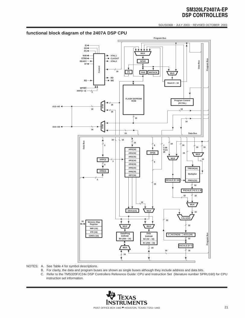
DSP CPU core
The 240xA devices use an advanced Harvard-type architecture that maximizes processing power bymaintaining two separate memory bus structures — program and data — for full-speed execution. This multiplebus structure allows data and instructions to be read simultaneously. Instructions support data transfersbetween program memory and data memory. This architecture permits coefficients that are stored in programmemory to be read in RAM, thereby eliminating the need for a separate coefficient ROM. This, coupled with afour-deep pipeline, allows the LF240xA/LC240xA devices to execute most instructions in a single cycle. Seethe functional block diagram of the 240xA DSP CPU for more information.
240xA instruction set
The 240xA microprocessor implements a comprehensive instruction set that supports both numeric-intensivesignal-processing operations and general-purpose applications, such as multiprocessing and high-speedcontrol.
For maximum throughput, the next instruction is prefetched while the current one is being executed. Becausethe same data lines are used to communicate to external data, program, or I/O space, the number of cycles aninstruction requires to execute varies, depending upon whether the next data operand fetch is from internal orexternal memory. Highest throughput is achieved by maintaining data memory on chip and using either internalor fast external program memory.
addressing modes
The 240xA instruction set provides four basic memory-addressing modes: direct, indirect, immediate, andregister.
In direct addressing, the instruction word contains the lower seven bits of the data memory address. This fieldis concatenated with the nine bits of the data memory page pointer (DP) to form the 16-bit data memory address.Therefore, in the direct-addressing mode, data memory is paged effectively with a total of 512 pages, with eachpage containing 128 words.
Indirect addressing accesses data memory through the auxiliary registers. In this addressing mode, the addressof the instruction operand is contained in the currently selected auxiliary register. Eight auxiliary registers(AR0−AR7) provide flexible and powerful indirect addressing. To select a specific auxiliary register, the auxiliaryregister pointer (ARP) is loaded with a value from 0 to 7 for AR0 through AR7, respectively.
scan-based emulation
x2xx devices incorporate scan-based emulation logic for code-development and hardware-development support. Scan-based emulation allows the emulator to control the processor in the system withoutthe use of intrusive cables to the full pinout of the device. The scan-based emulator communicates with the x2xxby way of the IEEE 1149.1-compatible (JTAG) interface. The 240xA DSPs do not include boundary scan. Thescan chain of these devices is useful for emulation function only.
SGUS036B − JULY 2003 − REVISED OCTOBER 2003
21POST OFFICE BOX 1443 • HOUSTON, TEXAS 77251−1443
functional block diagram of the 2407A DSP CPU
32
16
Data Bus
16
OSCALE (0−7)
D15−D0
A15−A0
16
1616
32
32
ACCL(16)ACCH(16)C
32
CALU(32)
3232
MUX
ISCALE (0−16)
16
MUX
PREG(32)
Multiplier
TREG0(16)
MUX
16
16
MUX
B1 (256 × 16)
B2 (32 × 16)DARAM
B0 (256 × 16)DARAM
7LSBfromIR
MUX
DP(9)
9
9
MUX
1616
ARAU(16)
16
3
3
3
3
ARB(3)
ARP(3)
Program Bus
16
16
16
16
AR7(16)
AR6(16)
AR5(16)
AR3(16)
AR2(16)
AR1(16)
AR0(16)
Stack 8 × 16
PC
MUX
WERD
16
XTAL2CLKOUTXTAL1
2XINT[1−2]
MP/MC
RS
XFREADY
STRBR/W
PSDSIS
Con
trol Dat
a B
us
Pro
gram
Bus
Dat
a B
us
AR4(16)
16M
UX
MU
X
Data/Prog
16
PSCALE (−6, 0, 1, 4)
16
Data
32
16
16
16
16
16
FLASH EEPROM/ROM
MUX
MUX
NPAR
PAR MSTACK
Program Control(PCTRL)
Memory MapRegister
IMR (16)
IFR (16)
GREG (16)
16
Pro
gram
Bus
NOTES: A. See Table 4 for symbol descriptions.B. For clarity, the data and program buses are shown as single buses although they include address and data bits.C. Refer to the TMS320F/C24x DSP Controllers Reference Guide: CPU and Instruction Set (literature number SPRU160) for CPU
instruction set information.
SGUS036B − JULY 2003 − REVISED OCTOBER 2003
22 POST OFFICE BOX 1443 • HOUSTON, TEXAS 77251−1443
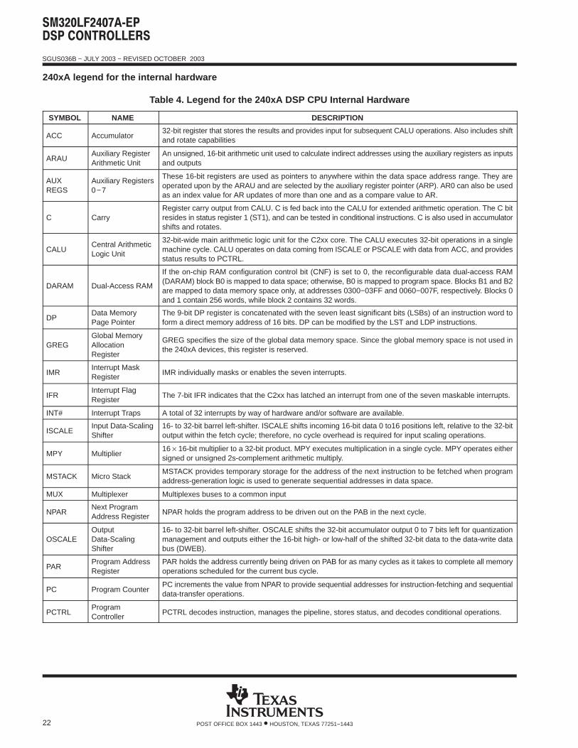
240xA legend for the internal hardware
Table 4. Legend for the 240xA DSP CPU Internal Hardware
SYMBOL NAME DESCRIPTION
ACC Accumulator32-bit register that stores the results and provides input for subsequent CALU operations. Also includes shiftand rotate capabilities
ARAUAuxiliary RegisterArithmetic Unit
An unsigned, 16-bit arithmetic unit used to calculate indirect addresses using the auxiliary registers as inputsand outputs
AUXREGS
Auxiliary Registers0−7
These 16-bit registers are used as pointers to anywhere within the data space address range. They areoperated upon by the ARAU and are selected by the auxiliary register pointer (ARP). AR0 can also be usedas an index value for AR updates of more than one and as a compare value to AR.
C CarryRegister carry output from CALU. C is fed back into the CALU for extended arithmetic operation. The C bitresides in status register 1 (ST1), and can be tested in conditional instructions. C is also used in accumulatorshifts and rotates.
CALUCentral ArithmeticLogic Unit
32-bit-wide main arithmetic logic unit for the C2xx core. The CALU executes 32-bit operations in a singlemachine cycle. CALU operates on data coming from ISCALE or PSCALE with data from ACC, and providesstatus results to PCTRL.
DARAM Dual-Access RAM
If the on-chip RAM configuration control bit (CNF) is set to 0, the reconfigurable data dual-access RAM(DARAM) block B0 is mapped to data space; otherwise, B0 is mapped to program space. Blocks B1 and B2are mapped to data memory space only, at addresses 0300−03FF and 0060−007F, respectively. Blocks 0and 1 contain 256 words, while block 2 contains 32 words.
DPData MemoryPage Pointer
The 9-bit DP register is concatenated with the seven least significant bits (LSBs) of an instruction word toform a direct memory address of 16 bits. DP can be modified by the LST and LDP instructions.
GREGGlobal MemoryAllocationRegister
GREG specifies the size of the global data memory space. Since the global memory space is not used inthe 240xA devices, this register is reserved.
IMRInterrupt MaskRegister
IMR individually masks or enables the seven interrupts.
IFRInterrupt FlagRegister
The 7-bit IFR indicates that the C2xx has latched an interrupt from one of the seven maskable interrupts.
INT# Interrupt Traps A total of 32 interrupts by way of hardware and/or software are available.
ISCALEInput Data-ScalingShifter
16- to 32-bit barrel left-shifter. ISCALE shifts incoming 16-bit data 0 to16 positions left, relative to the 32-bitoutput within the fetch cycle; therefore, no cycle overhead is required for input scaling operations.
MPY Multiplier16 × 16-bit multiplier to a 32-bit product. MPY executes multiplication in a single cycle. MPY operates eithersigned or unsigned 2s-complement arithmetic multiply.
MSTACK Micro StackMSTACK provides temporary storage for the address of the next instruction to be fetched when programaddress-generation logic is used to generate sequential addresses in data space.
MUX Multiplexer Multiplexes buses to a common input
NPARNext ProgramAddress Register
NPAR holds the program address to be driven out on the PAB in the next cycle.
OSCALEOutputData-ScalingShifter
16- to 32-bit barrel left-shifter. OSCALE shifts the 32-bit accumulator output 0 to 7 bits left for quantizationmanagement and outputs either the 16-bit high- or low-half of the shifted 32-bit data to the data-write databus (DWEB).
PARProgram AddressRegister
PAR holds the address currently being driven on PAB for as many cycles as it takes to complete all memoryoperations scheduled for the current bus cycle.
PC Program CounterPC increments the value from NPAR to provide sequential addresses for instruction-fetching and sequentialdata-transfer operations.
PCTRLProgramController
PCTRL decodes instruction, manages the pipeline, stores status, and decodes conditional operations.
SGUS036B − JULY 2003 − REVISED OCTOBER 2003
23POST OFFICE BOX 1443 • HOUSTON, TEXAS 77251−1443
240xA legend for the internal hardware (continued)
Table 4. Legend for the 240xA DSP CPU Internal Hardware (Continued)
SYMBOL NAME DESCRIPTION
PREG Product Register 32-bit register holds results of 16 × 16 multiply
PSCALEProduct-ScalingShifter
0-, 1-, or 4-bit left shift, or 6-bit right shift of multiplier product. The left-shift options are used to manage theadditional sign bits resulting from the 2s-complement multiply. The right-shift option is used to scale downthe number to manage overflow of product accumulation in the CALU. PSCALE resides in the path from the32-bit product shifter and from either the CALU or the data-write data bus (DWEB), and requires no cycleoverhead.
STACK StackSTACK is a block of memory used for storing return addresses for subroutines and interrupt-serviceroutines, or for storing data. The C2xx stack is 16 bits wide and 8 levels deep.
TREGTemporaryRegister
16-bit register holds one of the operands for the multiply operations. TREG holds the dynamic shift countfor the LACT, ADDT, and SUBT instructions. TREG holds the dynamic bit position for the BITT instruction.
status and control registers
Two status registers, ST0 and ST1, contain the status of various conditions and modes. These registers canbe stored into data memory and loaded from data memory, thus allowing the status of the machine to be savedand restored for subroutines.
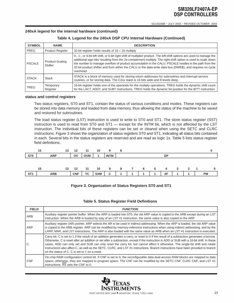
The load status register (LST) instruction is used to write to ST0 and ST1. The store status register (SST)instruction is used to read from ST0 and ST1 — except for the INTM bit, which is not affected by the LSTinstruction. The individual bits of these registers can be set or cleared when using the SETC and CLRCinstructions. Figure 3 shows the organization of status registers ST0 and ST1, indicating all status bits containedin each. Several bits in the status registers are reserved and are read as logic 1s. Table 5 lists status registerfield definitions.
15 13 12 11 10 9 8 0
ST0 ARP OV OVM 1 INTM DP
15 13 12 11 10 9 8 7 6 5 4 3 2 1 0
ST1 ARB CNF TC SXM C 1 1 1 1 XF 1 1 PM
Figure 3. Organization of Status Registers ST0 and ST1
Table 5. Status Register Field Definitions
FIELD FUNCTION
ARBAuxiliary register pointer buffer. When the ARP is loaded into ST0, the old ARP value is copied to the ARB except during an LSTinstruction. When the ARB is loaded by way of an LST #1 instruction, the same value is also copied to the ARP.
ARPAuxiliary register (AR) pointer. ARP selects the AR to be used in indirect addressing. When the ARP is loaded, the old ARP valueis copied to the ARB register. ARP can be modified by memory-reference instructions when using indirect addressing, and by theLARP, MAR, and LST instructions. The ARP is also loaded with the same value as ARB when an LST #1 instruction is executed.
C
Carry bit. C is set to 1 if the result of an addition generates a carry, or reset to 0 if the result of a subtraction generates a borrow.Otherwise, C is reset after an addition or set after a subtraction, except if the instruction is ADD or SUB with a 16-bit shift. In thesecases, ADD can only set and SUB can only reset the carry bit, but cannot affect it otherwise. The single-bit shift and rotateinstructions also affect C, as well as the SETC, CLRC, and LST #1 instructions. Branch instructions have been provided to branchon the status of C. C is set to 1 on a reset.
CNFOn-chip RAM configuration control bit. If CNF is set to 0, the reconfigurable data dual-access RAM blocks are mapped to dataspace; otherwise, they are mapped to program space. The CNF can be modified by the SETC CNF, CLRC CNF, and LST #1instructions. RS sets the CNF to 0.
SGUS036B − JULY 2003 − REVISED OCTOBER 2003
24 POST OFFICE BOX 1443 • HOUSTON, TEXAS 77251−1443
status and control registers (continued)
Table 5. Status Register Field Definitions (Continued)
FIELD FUNCTION
DPData memory page pointer. The 9-bit DP register is concatenated with the 7 LSBs of an instruction word to form a direct memoryaddress of 16 bits. DP can be modified by the LST and LDP instructions.
INTM
Interrupt mode bit. When INTM is set to 0, all unmasked interrupts are enabled. When set to 1, all maskable interrupts are disabled.INTM is set and reset by the SETC INTM and CLRC INTM instructions. RS also sets INTM. INTM has no effect on the unmaskableRS and NMI interrupts. Note that INTM is unaffected by the LST instruction. This bit is set to 1 by reset. It is also set to 1 whena maskable interrupt trap is taken.
OVOverflow flag bit. As a latched overflow signal, OV is set to 1 when overflow occurs in the arithmetic logic unit (ALU). Once anoverflow occurs, the OV remains set until a reset, BCND/D on OV/NOV, or LST instruction clears OV.
OVMOverflow mode bit. When OVM is set to 0, overflowed results overflow normally in the accumulator. When set to 1, the accumulatoris set to either its most positive or negative value upon encountering an overflow. The SETC and CLRC instructions set and resetthis bit, respectively. LST can also be used to modify the OVM.
PM
Product shift mode. If these two bits are 00, the multiplier’s 32-bit product is loaded into the ALU with no shift. If PM = 01, the PREGoutput is left-shifted one place and loaded into the ALU, with the LSB zero-filled. If PM = 10, the PREG output is left-shifted by 4 bitsand loaded into the ALU, with the LSBs zero-filled. PM = 11 produces a right shift of 6 bits, sign-extended. Note that the PREGcontents remain unchanged. The shift takes place when transferring the contents of the PREG to the ALU. PM is loaded by theSPM and LST #1 instructions. PM is cleared by RS.
SXM
Sign-extension mode bit. SXM = 1 produces sign extension on data as it is passed into the accumulator through the scaling shifter.SXM = 0 suppresses sign extension. SXM does not affect the definitions of certain instructions; for example, the ADDS instructionsuppresses sign extension regardless of SXM. SXM is set by the SETC SXM instruction and reset by the CLRC SXM instructionand can be loaded by the LST #1 instruction. SXM is set to 1 by reset.
TC
Test/control flag bit. TC is affected by the BIT, BITT, CMPR, LST #1, and NORM instructions. TC is set to a 1 if a bit tested by BITor BITT is a 1, if a compare condition tested by CMPR exists between AR (ARP) and AR0, if the exclusive-OR function of the 2 mostsignificant bits (MSBs) of the accumulator is true when tested by a NORM instruction. The conditional branch, call, and returninstructions can execute based on the condition of TC.
XFXF pin status bit. XF indicates the state of the XF pin, a general-purpose output pin. XF is set by the SETC XF instruction and resetby the CLRC XF instruction. XF is set to 1 by reset.
central processing unit
The 240xA central processing unit (CPU) contains a 16-bit scaling shifter, a 16 x 16-bit parallel multiplier, a 32-bitcentral arithmetic logic unit (CALU), a 32-bit accumulator, and additional shifters at the outputs of both theaccumulator and the multiplier. This section describes the CPU components and their functions. The functionalblock diagram shows the components of the CPU.
input scaling shifter
The 240xA provides a scaling shifter with a 16-bit input connected to the data bus and a 32-bit output connectedto the CALU. This shifter operates as part of the path of data coming from program or data space to the CALUand requires no cycle overhead. It is used to align the 16-bit data coming from memory to the 32-bit CALU. Thisis necessary for scaling arithmetic as well as aligning masks for logical operations.
The scaling shifter produces a left shift of 0 to 16 on the input data. The LSBs of the output are filled with zeros;the MSBs can either be filled with zeros or sign-extended, depending upon the value of the SXM bit(sign-extension mode) of status register ST1. The shift count is specified by a constant embedded in theinstruction word or by a value in TREG. The shift count in the instruction allows for specific scaling or alignmentoperations specific to that point in the code. The TREG base shift allows the scaling factor to be adaptable tothe system’s performance.
SGUS036B − JULY 2003 − REVISED OCTOBER 2003
25POST OFFICE BOX 1443 • HOUSTON, TEXAS 77251−1443
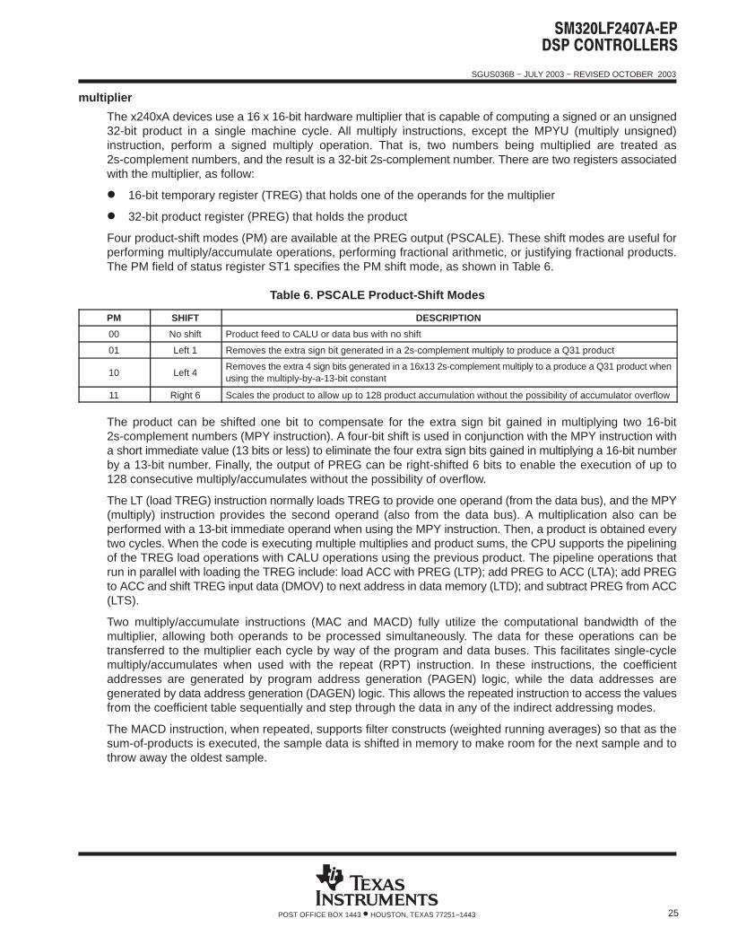
multiplier
The x240xA devices use a 16 x 16-bit hardware multiplier that is capable of computing a signed or an unsigned32-bit product in a single machine cycle. All multiply instructions, except the MPYU (multiply unsigned)instruction, perform a signed multiply operation. That is, two numbers being multiplied are treated as2s-complement numbers, and the result is a 32-bit 2s-complement number. There are two registers associatedwith the multiplier, as follow:
16-bit temporary register (TREG) that holds one of the operands for the multiplier
32-bit product register (PREG) that holds the product
Four product-shift modes (PM) are available at the PREG output (PSCALE). These shift modes are useful forperforming multiply/accumulate operations, performing fractional arithmetic, or justifying fractional products.The PM field of status register ST1 specifies the PM shift mode, as shown in Table 6.
Table 6. PSCALE Product-Shift Modes
PM SHIFT DESCRIPTION
00 No shift Product feed to CALU or data bus with no shift
01 Left 1 Removes the extra sign bit generated in a 2s-complement multiply to produce a Q31 product
10 Left 4Removes the extra 4 sign bits generated in a 16x13 2s-complement multiply to a produce a Q31 product whenusing the multiply-by-a-13-bit constant
11 Right 6 Scales the product to allow up to 128 product accumulation without the possibility of accumulator overflow
The product can be shifted one bit to compensate for the extra sign bit gained in multiplying two 16-bit2s-complement numbers (MPY instruction). A four-bit shift is used in conjunction with the MPY instruction witha short immediate value (13 bits or less) to eliminate the four extra sign bits gained in multiplying a 16-bit numberby a 13-bit number. Finally, the output of PREG can be right-shifted 6 bits to enable the execution of up to128 consecutive multiply/accumulates without the possibility of overflow.
The LT (load TREG) instruction normally loads TREG to provide one operand (from the data bus), and the MPY(multiply) instruction provides the second operand (also from the data bus). A multiplication also can beperformed with a 13-bit immediate operand when using the MPY instruction. Then, a product is obtained everytwo cycles. When the code is executing multiple multiplies and product sums, the CPU supports the pipeliningof the TREG load operations with CALU operations using the previous product. The pipeline operations thatrun in parallel with loading the TREG include: load ACC with PREG (LTP); add PREG to ACC (LTA); add PREGto ACC and shift TREG input data (DMOV) to next address in data memory (LTD); and subtract PREG from ACC(LTS).
Two multiply/accumulate instructions (MAC and MACD) fully utilize the computational bandwidth of themultiplier, allowing both operands to be processed simultaneously. The data for these operations can betransferred to the multiplier each cycle by way of the program and data buses. This facilitates single-cyclemultiply/accumulates when used with the repeat (RPT) instruction. In these instructions, the coefficientaddresses are generated by program address generation (PAGEN) logic, while the data addresses aregenerated by data address generation (DAGEN) logic. This allows the repeated instruction to access the valuesfrom the coefficient table sequentially and step through the data in any of the indirect addressing modes.
The MACD instruction, when repeated, supports filter constructs (weighted running averages) so that as thesum-of-products is executed, the sample data is shifted in memory to make room for the next sample and tothrow away the oldest sample.
SGUS036B − JULY 2003 − REVISED OCTOBER 2003
26 POST OFFICE BOX 1443 • HOUSTON, TEXAS 77251−1443
multiplier (continued)
The MPYU instruction performs an unsigned multiplication, which greatly facilitates extended-precisionarithmetic operations. The unsigned contents of TREG are multiplied by the unsigned contents of the addresseddata memory location, with the result placed in PREG. This process allows the operands of greater than 16 bitsto be broken down into 16-bit words and processed separately to generate products of greater than 32 bits. TheSQRA (square/add) and SQRS (square/subtract) instructions pass the same value to both inputs of themultiplier for squaring a data memory value.
After the multiplication of two 16-bit numbers, the 32-bit product is loaded into the 32-bit product register(PREG). The product from PREG can be transferred to the CALU or to data memory by way of the SPH (storeproduct high) and SPL (store product low) instructions. Note: the transfer of PREG to either the CALU or databus passes through the PSCALE shifter, and therefore is affected by the product shift mode defined by PM. Thisis important when saving PREG in an interrupt-service-routine context save as the PSCALE shift effects cannotbe modeled in the restore operation. PREG can be cleared by executing the MPY #0 instruction. The productregister can be restored by loading the saved low half into TREG and executing a MPY #1 instruction. The highhalf, then, is loaded using the LPH instruction.
central arithmetic logic unit
The x240xA central arithmetic logic unit (CALU) implements a wide range of arithmetic and logical functions,the majority of which execute in a single clock cycle. This ALU is referred to as central to differentiate it froma second ALU used for indirect-address generation called the auxiliary register arithmetic unit (ARAU). Oncean operation is performed in the CALU, the result is transferred to the accumulator (ACC) where additionaloperations, such as shifting, can occur. Data that is input to the CALU can be scaled by ISCALE when comingfrom one of the data buses (DRDB or PRDB) or scaled by PSCALE when coming from the multiplier.
The CALU is a general-purpose ALU that operates on 16-bit words taken from data memory or derived fromimmediate instructions. In addition to the usual arithmetic instructions, the CALU can perform Booleanoperations, facilitating the bit-manipulation ability required for a high-speed controller. One input to the CALUis always provided from the accumulator, and the other input can be provided from the product register (PREG)of the multiplier or the output of the scaling shifter (that has been read from data memory or from the ACC). Afterthe CALU has performed the arithmetic or logical operation, the result is stored in the accumulator.
The x240xA devices support floating-point operations for applications requiring a large dynamic range. TheNORM (normalization) instruction is used to normalize fixed-point numbers contained in the accumulator byperforming left shifts. The four bits of the TREG define a variable shift through the scaling shifter for theLACT/ADDT/SUBT (load/add to/subtract from accumulator with shift specified by TREG) instructions. Theseinstructions are useful in floating-point arithmetic where a number needs to be denormalized — that is,floating-point to fixed-point conversion. They are also useful in the execution of an automatic gain control (AGC)going into a filter. The BITT (bit test) instruction provides testing of a single bit of a word in data memory basedon the value contained in the four LSBs of TREG.
The CALU overflow saturation mode can be enabled/disabled by setting/resetting the OVM bit of ST0. Whenthe CALU is in the overflow saturation mode and an overflow occurs, the overflow flag is set and the accumulatoris loaded with either the most positive or the most negative value representable in the accumulator, dependingon the direction of the overflow. The value of the accumulator at saturation is 07FFFFFFFh (positive) or080000000h (negative). If the OVM (overflow mode) status register bit is reset and an overflow occurs, theoverflowed results are loaded into the accumulator with modification. (Note that logical operations cannot resultin overflow.)
The CALU can execute a variety of branch instructions that depend on the status of the CALU and theaccumulator. These instructions can be executed conditionally based on any meaningful combination of thesestatus bits. For overflow management, these conditions include OV (branch on overflow) and EQ (branch onaccumulator equal to zero). In addition, the BACC (branch to address in accumulator) instruction provides theability to branch to an address specified by the accumulator (computed goto). Bit test instructions (BIT andBITT), which do not affect the accumulator, allow the testing of a specified bit of a word in data memory.
SGUS036B − JULY 2003 − REVISED OCTOBER 2003
27POST OFFICE BOX 1443 • HOUSTON, TEXAS 77251−1443
central arithmetic logic unit (continued)
The CALU also has an associated carry bit that is set or reset depending on various operations within the device.The carry bit allows more efficient computation of extended-precision products and additions or subtractions.It is also useful in overflow management. The carry bit is affected by most arithmetic instructions as well as thesingle-bit shift and rotate instructions. It is not affected by loading the accumulator, logical operations, or othersuch non-arithmetic or control instructions.
The ADDC (add to accumulator with carry) and SUBB (subtract from accumulator with borrow) instructions usethe previous value of carry in their addition/subtraction operation.
The one exception to the operation of the carry bit is in the use of ADD with a shift count of 16 (add to highaccumulator) and SUB with a shift count of 16 (subtract from high accumulator) instructions. This case of theADD instruction can set the carry bit only if a carry is generated, and this case of the SUB instruction can resetthe carry bit only if a borrow is generated; otherwise, neither instruction affects it.
Two conditional operands, C and NC, are provided for branching, calling, returning, and conditionally executing,based upon the status of the carry bit. The SETC, CLRC, and LST #1 instructions also can be used to load thecarry bit. The carry bit is set to one on a hardware reset.
accumulator
The 32-bit accumulator is the registered output of the CALU. It can be split into two 16-bit segments for storagein data memory. Shifters at the output of the accumulator provide a left shift of 0 to 7 places. This shift isperformed while the data is being transferred to the data bus for storage. The contents of the accumulatorremain unchanged. When the postscaling shifter is used on the high word of the accumulator (bits 16−31), theMSBs are lost and the LSBs are filled with bits shifted in from the low word (bits 0−15). When the postscalingshifter is used on the low word, the LSBs are zero-filled.
The SFL and SFR (in-place one-bit shift to the left / right) instructions and the ROL and ROR (rotate to theleft/right) instructions implement shifting or rotating of the contents of the accumulator through the carry bit. TheSXM bit affects the definition of the SFR (shift accumulator right) instruction. When SXM = 1, SFR performs anarithmetic right shift, maintaining the sign of the accumulator data. When SXM = 0, SFR performs a logical shift,shifting out the LSBs and shifting in a zero for the MSB. The SFL (shift accumulator left) instruction is not affectedby the SXM bit and behaves the same in both cases, shifting out the MSB and shifting in a zero. Repeat (RPT)instructions can be used with the shift and rotate instructions for multiple-bit shifts.
auxiliary registers and auxiliary-register arithmetic unit (ARAU)
The 240xA provides a register file containing eight auxiliary registers (AR0−AR7). The auxiliary registers areused for indirect addressing of the data memory or for temporary data storage. Indirect auxiliary-registeraddressing allows placement of the data memory address of an instruction operand into one of the auxiliaryregisters. These registers are referenced with a 3-bit auxiliary register pointer (ARP) that is loaded with a valuefrom 0 through 7, designating AR0 through AR7, respectively. The auxiliary registers and the ARP can be loadedfrom data memory, the ACC, the product register, or by an immediate operand defined in the instruction. Thecontents of these registers also can be stored in data memory or used as inputs to the CALU.
The auxiliary register file (AR0−AR7) is connected to the ARAU. The ARAU can autoindex the current auxiliaryregister while the data memory location is being addressed. Indexing either by ±1 or by the contents of the AR0register can be performed. As a result, accessing tables of information does not require the CALU for addressmanipulation; therefore, the CALU is free for other operations in parallel.
SGUS036B − JULY 2003 − REVISED OCTOBER 2003
28 POST OFFICE BOX 1443 • HOUSTON, TEXAS 77251−1443
internal memory
The 320x240xA devices are configured with the following memory modules:
Dual-access random-access memory (DARAM)
Single-access random-access memory (SARAM)
Flash
ROM
Boot ROM
dual-access RAM (DARAM)
There are 544 words × 16 bits of DARAM on the 240xA devices. The 240xA DARAM allows writes to and readsfrom the RAM in the same cycle. The DARAM is configured in three blocks: block 0 (B0), block 1 (B1), andblock 2 (B2). Block 1 contains 256 words and Block 2 contains 32 words, and both blocks are located only indata memory space. Block 0 contains 256 words, and can be configured to reside in either data or programmemory space. The SETC CNF (configure B0 as program memory) and CLRC CNF (configure B0 as datamemory) instructions allow dynamic configuration of the memory maps through software.
When using on-chip RAM, the 240xA runs at full speed with no wait states. The ability of the DARAM to allowtwo accesses to be performed in one cycle, coupled with the parallel nature of the 240xA architecture, enablesthe device to perform three concurrent memory accesses in any given machine cycle. Externally, the READYline or on-chip software wait-state generator can be used to interface the 2407A to slower, less expensiveexternal memory.
single-access RAM (SARAM)
There are 2K words × 16 bits of SARAM on the 2407A.† The PON and DON bits select SARAM (2K) mappingin program space, data space, or both. See Table 18 for details on the SCSR2 register and the PON and DONbits. At reset, these bits are 11, and the on-chip SARAM is mapped in both the program and data spaces. TheSARAM (starting at 8000h in program memory) is accessible in external memory space, if the on-chip SARAMis not enabled.
flash EEPROM
Flash EEPROM provides an attractive alternative to masked program ROM. Like ROM, Flash is nonvolatile.However, it has the advantage of “in-target” reprogrammability. The LF2407A incorporates one 32K 16-bitFlash EEPROM module in program space. The Flash module has multiple sectors that can be individuallyprotected while erasing or programming. The sector size is non-uniform and partitioned as 4K/12K/12K/4Ksectors.
Unlike most discrete Flash memory, the LF240xA Flash does not require a dedicated state machine, becausethe algorithms for programming and erasing the Flash are executed by the DSP core. This enables severaladvantages, including: reduced chip size and sophisticated, adaptive algorithms. For production programming,the IEEE Standard 1149.1‡ (JTAG) scan port provides easy access to the on-chip RAM for downloading thealgorithms and Flash code. This Flash requires 5 V for programming (at VCCP pin only) the array. The Flash runsat zero wait state while the device is powered at 3.3 V.
† See Table 1 for device-specific features.‡ IEEE Standard 1149.1−1990, IEEE Standard Test Access Port.
SGUS036B − JULY 2003 − REVISED OCTOBER 2003
29POST OFFICE BOX 1443 • HOUSTON, TEXAS 77251−1443
boot ROM
Boot ROM is a 256-word ROM memory-mapped in program space 0000−00FF. This ROM will be enabled if theBOOT_EN pin is low during reset. The BOOT_EN bit (bit 3 of the SCSR2 register) will be set to 0 if the BOOT_ENpin is low at reset. Boot ROM can also be enabled by writing 0 to the SCSR2.3 bit and disabled by writing 1 tothis bit.
The boot ROM has a generic bootloader to transfer code through SCI or SPI ports. The incoming code shoulddisable the BOOT_ROM bit by writing 1 to bit 3 of the SCSR2 register, or else, the whole Flash array will notbe enabled.
The boot ROM code sets the PLL to x2 or x4 option based on the condition of the SCITXD pin during reset. TheSCITXD pin should be pulled high/low to select the PLL multiplication factor. The choices made are as follows:
If the SCITXD pin is pulled low, the PLL multiplier is set to 2.
If the SCITXD pin is pulled high, the PLL multiplier is set to 4. (Default)
If the SCITXD pin is not driven at reset, the internal pullup selects the default multiplier of 4.
Care should be taken such that a combination of CLKIN and the PLL multiplication factor should not result ina CPU clock speed of greater than 40 MHz, the maximum rated speed.
Furthermore, when the bootloader is used, only specific values of CLKIN would result in a baud-lock for the SCI.Refer to the TMS320LF/LC240xA DSP Controllers Reference Guide: System and Peripherals (literaturenumber SPRU357) for more details about the bootloader operation.
SGUS036B − JULY 2003 − REVISED OCTOBER 2003
30 POST OFFICE BOX 1443 • HOUSTON, TEXAS 77251−1443
flash/ROM security
240xA devices incorporate a security feature that prevents external access to program memory. This featureis useful in preventing unauthorized duplication of proprietary code.
If access to Flash/ROM contents are desired for debugging purposes, two actions need to be taken:
1. A “dummy” read of locations 40h, 41h, 42h and 43h (of program memory space) is necessary. The word“dummy” indicates that the destination address of this read is insignificant.
NOTE: Step 2 is not required if 40h−43h contain 0000 0000 0000 0000h or FFFF FFFF FFFF FFFFh.
2. A 64-bit password (split as four 16-bit words) must be written to the data-memory locations 77F0h, 77F1h,77F2h, and 77F3h. The four 16-bit words written to these locations must match the four words stored in 40h,41h, 42h, and 43h (of program memory space), respectively. The device becomes “unsecured” one cycleafter the last instruction that unsecures the part.
Code Security Module Disclaimer
The Code Security Module (“CSM”) included on this device was designed to passwordprotect the data stored in the associated memory (either ROM or Flash) and is warrantedby Texas Instruments (TI), in accordance with its standard terms and conditions, toconform to TI’s published specifications for the warranty period applicable for this device.
TI DOES NOT, HOWEVER, WARRANT OR REPRESENT THAT THE CSM CANNOT BECOMPROMISED OR BREACHED OR THAT THE DATA STORED IN THEASSOCIATED MEMORY CANNOT BE ACCESSED THROUGH OTHER MEANS.MOREOVER, EXCEPT AS SET FORTH ABOVE, TI MAKES NO WARRANTIES ORREPRESENTATIONS CONCERNING THE CSM OR OPERATION OF THIS DEVICE,INCLUDING ANY IMPLIED WARRANTIES OF MERCHANTABILITY OR FITNESS FORA PARTICULAR PURPOSE.
IN NO EVENT SHALL TI BE LIABLE FOR ANY CONSEQUENTIAL, SPECIAL,INDIRECT, INCIDENTAL, OR PUNITIVE DAMAGES, HOWEVER CAUSED, ARISINGIN ANY WAY OUT OF YOUR USE OF THE CSM OR THIS DEVICE, WHETHER OR NOTTI HAS BEEN ADVISED OF THE POSSIBILITY OF SUCH DAMAGES. EXCLUDEDDAMAGES INCLUDE, BUT ARE NOT LIMITED TO LOSS OF DATA, LOSS OFGOODWILL, LOSS OF USE OR INTERRUPTION OF BUSINESS OR OTHERECONOMIC LOSS.
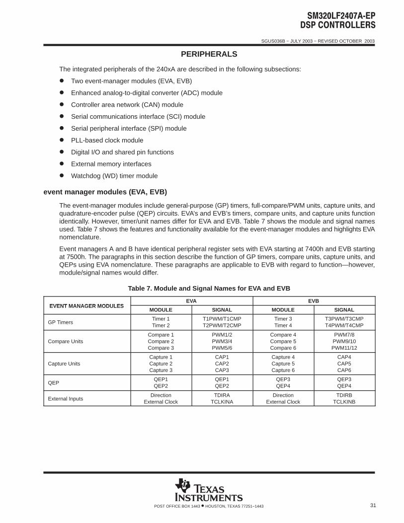
SGUS036B − JULY 2003 − REVISED OCTOBER 2003
31POST OFFICE BOX 1443 • HOUSTON, TEXAS 77251−1443
PERIPHERALS
The integrated peripherals of the 240xA are described in the following subsections:
Two event-manager modules (EVA, EVB)
Enhanced analog-to-digital converter (ADC) module
Controller area network (CAN) module
Serial communications interface (SCI) module
Serial peripheral interface (SPI) module
PLL-based clock module
Digital I/O and shared pin functions
External memory interfaces
Watchdog (WD) timer module
event manager modules (EVA, EVB)
The event-manager modules include general-purpose (GP) timers, full-compare/PWM units, capture units, andquadrature-encoder pulse (QEP) circuits. EVA’s and EVB’s timers, compare units, and capture units functionidentically. However, timer/unit names differ for EVA and EVB. Table 7 shows the module and signal namesused. Table 7 shows the features and functionality available for the event-manager modules and highlights EVAnomenclature.
Event managers A and B have identical peripheral register sets with EVA starting at 7400h and EVB startingat 7500h. The paragraphs in this section describe the function of GP timers, compare units, capture units, andQEPs using EVA nomenclature. These paragraphs are applicable to EVB with regard to function—however,module/signal names would differ.
Table 7. Module and Signal Names for EVA and EVB
EVENT MANAGER MODULESEVA EVB
EVENT MANAGER MODULESMODULE SIGNAL MODULE SIGNAL
GP TimersTimer 1Timer 2
T1PWM/T1CMPT2PWM/T2CMP
Timer 3Timer 4
T3PWM/T3CMPT4PWM/T4CMP
Compare UnitsCompare 1Compare 2Compare 3
PWM1/2PWM3/4PWM5/6
Compare 4Compare 5Compare 6
PWM7/8PWM9/10PWM11/12
Capture UnitsCapture 1Capture 2Capture 3
CAP1CAP2CAP3
Capture 4Capture 5Capture 6
CAP4CAP5CAP6
QEPQEP1QEP2
QEP1QEP2
QEP3QEP4
QEP3QEP4
External InputsDirection
External ClockTDIRA
TCLKINADirection
External ClockTDIRB
TCLKINB
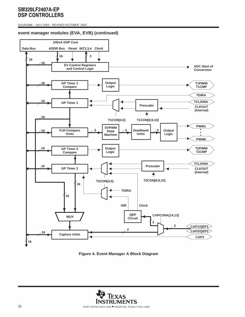
SGUS036B − JULY 2003 − REVISED OCTOBER 2003
32 POST OFFICE BOX 1443 • HOUSTON, TEXAS 77251−1443
event manager modules (EVA, EVB) (continued)
Data Bus ADDR Bus Reset INT2,3,4
OutputLogic
PWM1
PWM6
T2PWM/T2CMP
1616
16
16
16
16
16
16
16
16
16
3 3 3
ADC Start ofConversion
QEPCircuit
ClockDIR
16
16
2
Prescaler
TDIRA
TCLKINA
CLKOUT(Internal)
T1CON[8,9,10]T1CON[4,5]
T2CON[8,9,10]T2CON[4,5]
TCLKINA
TDIRA
OutputLogic
DeadbandUnits
SVPWMState
Machine
22
CAPCONA[14,13]
Capture Units
MUX
GP Timer 1
Full-CompareUnits
GP Timer 2Compare
GP Timer 2
EV Control Registersand Control Logic
GP Timer 1Compare
OutputLogic
Clock
240xA DSP Core
3
PrescalerCLKOUT(Internal)
CAP1/QEP1
CAP3
CAP2/QEP2
T1PWM/T1CMP
Figure 4. Event Manager A Block Diagram
SGUS036B − JULY 2003 − REVISED OCTOBER 2003
33POST OFFICE BOX 1443 • HOUSTON, TEXAS 77251−1443
general-purpose (GP) timers
There are two GP timers. The GP timer x (x = 1 or 2 for EVA; x = 3 or 4 for EVB) includes:
A 16-bit timer, up-/down-counter, TxCNT, for reads or writes
A 16-bit timer-compare register, TxCMPR (double-buffered with shadow register), for reads or writes
A 16-bit timer-period register, TxPR (double-buffered with shadow register), for reads or writes
A 16-bit timer-control register,TxCON, for reads or writes
Selectable internal or external input clocks
A programmable prescaler for internal or external clock inputs
Control and interrupt logic, for four maskable interrupts: underflow, overflow, timer compare, and periodinterrupts
A selectable direction input pin (TDIRx) (to count up or down when directional up-/down-count mode isselected)
The GP timers can be operated independently or synchronized with each other. The compare registerassociated with each GP timer can be used for compare function and PWM-waveform generation. There arethree continuous modes of operations for each GP timer in up- or up/down-counting operations. Internal orexternal input clocks with programmable prescaler are used for each GP timer. GP timers also provide the timebase for the other event-manager submodules: GP timer 1 for all the compares and PWM circuits, GP timer 2/1for the capture units and the quadrature-pulse counting operations. Double-buffering of the period and compareregisters allows programmable change of the timer (PWM) period and the compare/PWM pulse width asneeded.
full-compare units
There are three full-compare units on each event manager. These compare units use GP timer1 as the timebase and generate six outputs for compare and PWM-waveform generation using programmable deadbandcircuit. The state of each of the six outputs is configured independently. The compare registers of the compareunits are double-buffered, allowing programmable change of the compare/PWM pulse widths as needed.
programmable deadband generator
The deadband generator circuit includes three 8-bit counters and an 8-bit compare register. Desired deadbandvalues (from 0 to 16 µs) can be programmed into the compare register for the outputs of the three compare units.The deadband generation can be enabled/disabled for each compare unit output individually. Thedeadband-generator circuit produces two outputs (with or without deadband zone) for each compare unit outputsignal. The output states of the deadband generator are configurable and changeable as needed by way of thedouble-buffered ACTR register.
PWM waveform generation
Up to eight PWM waveforms (outputs) can be generated simultaneously by each event manager: threeindependent pairs (six outputs) by the three full-compare units with programmable deadbands, and twoindependent PWMs by the GP-timer compares.
SGUS036B − JULY 2003 − REVISED OCTOBER 2003
34 POST OFFICE BOX 1443 • HOUSTON, TEXAS 77251−1443
PWM characteristics
Characteristics of the PWMs are as follows:
16-bit registers
Programmable deadband for the PWM output pairs, from 0 to 12 µs
Minimum deadband width of 25 ns
Change of the PWM carrier frequency for PWM frequency wobbling as needed
Change of the PWM pulse widths within and after each PWM period as needed
External-maskable power and drive-protection interrupts
Pulse-pattern-generator circuit, for programmable generation of asymmetric, symmetric, and four-spacevector PWM waveforms
Minimized CPU overhead using auto-reload of the compare and period registers
The PWM pins are driven to a high-impedance state when the PDPINTx pin is driven low and after PDPINTxsignal qualification. The PDPINTx pin (after qualification) is reflected in bit 8 of the COMCONx register.
− PDPINTA pin status is reflected in bit 8 of COMCONA register.
− PDPINTB pin status is reflected in bit 8 of COMCONB register.
capture unit
The capture unit provides a logging function for different events or transitions. The values of the selected GPtimer counter is captured and stored in the two-level-deep FIFO stacks when selected transitions are detectedon capture input pins, CAPx (x = 1, 2, or 3 for EVA; and x = 4, 5, or 6 for EVB). The capture unit consists of threecapture circuits.
Capture units include the following features:
One 16-bit capture control register, CAPCONx (R/W)
One 16-bit capture FIFO status register, CAPFIFOx
Selection of GP timer 1/2 (for EVA) or 3/4 (for EVB) as the time base
Three 16-bit 2-level-deep FIFO stacks, one for each capture unit
Three capture input pins (CAP1/2/3 for EVA, CAP4/5/6 for EVB)—one input pin per capture unit. [All inputsare synchronized with the device (CPU) clock. In order for a transition to be captured, the input must holdat its current level to meet two rising edges of the device clock. The input pins CAP1/2 and CAP4/5 can alsobe used as QEP inputs to the QEP circuit.]
User-specified transition (rising edge, falling edge, or both edges) detection
Three maskable interrupt flags, one for each capture unit
quadrature-encoder pulse (QEP) circuit
Two capture inputs (CAP1 and CAP2 for EVA; CAP4 and CAP5 for EVB) can be used to interface the on-chipQEP circuit with a quadrature encoder pulse. Full synchronization of these inputs is performed on-chip.Direction or leading-quadrature pulse sequence is detected, and GP timer 2/4 is incremented or decrementedby the rising and falling edges of the two input signals (four times the frequency of either input pulse).
SGUS036B − JULY 2003 − REVISED OCTOBER 2003
35POST OFFICE BOX 1443 • HOUSTON, TEXAS 77251−1443
input qualifier circuitry
An input-qualifier circuitry qualifies the input signal to the CAP1−6, XINT1/2, ADCSOC and PDPINTA/B pinsin the 240xA devices. (The I/O functions of these pins do not use the input-qualifier circuitry). The state of theinternal input signal will change only after the pin is high/low for 6(12) clock edges. This ensures that a glitchsmaller than 5(11) CLKOUT cycles wide will not change the internal pin input state. The user must hold the pinhigh/low for 6(12) cycles to ensure the device will see the level change. Bit 6 of the SCSR2 register controlswhether 6 clock edges (bit 6 = 0) or 12 clock edges (bit 6 = 1) are used to block 5- or 11-cycle glitches. On theLC2402A, input qualification is for the CAP1, CAP2, CAP3, PDPINTA, and XINT2/ADCSOC pins.
enhanced analog-to-digital converter (ADC) module
A simplified functional block diagram of the ADC module is shown in Figure 5. The ADC module consists of a10-bit ADC with a built-in sample-and-hold (S/H) circuit. Functions of the ADC module include:
10-bit ADC core with built-in S/H
16-channel, MUXed inputs
Autosequencing capability provides up to 16 “autoconversions” in a single session. Each conversion canbe programmed to select any 1 of 16 input channels
Sequencer can be operated as two independent 8-state sequencers or as one large 16-state sequencer(i.e., two cascaded 8-state sequencers)
Sixteen result registers (individually addressable) to store conversion values
− The digital value of the input analog voltage is derived by:
Digital Value 1023
Input Analog Voltage VREFLO
VREFHI VREFLO
Multiple triggers as sources for the start-of-conversion (SOC) sequence
− S/W − software immediate start
− EVA − Event manager A (multiple event sources within EVA)
− EVB − Event manager B (multiple event sources within EVB)
− Ext − External pin (ADCSOC)
Flexible interrupt control allows interrupt request on every end-of-sequence (EOS) or every other EOS
Sequencer can operate in “start/stop” mode, allowing multiple “time-sequenced triggers” to synchronizeconversions
EVA and EVB triggers can operate independently in dual-sequencer mode
Sample-and-hold (S/H) acquisition time window has separate prescale control
NOTE: The calibration and self-test features are not present in 240xA devices.
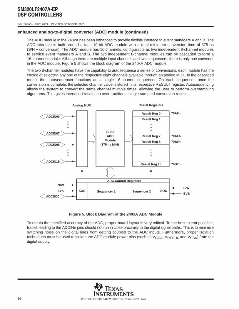
SGUS036B − JULY 2003 − REVISED OCTOBER 2003
36 POST OFFICE BOX 1443 • HOUSTON, TEXAS 77251−1443
enhanced analog-to-digital converter (ADC) module (continued)
The ADC module in the 240xA has been enhanced to provide flexible interface to event managers A and B. TheADC interface is built around a fast, 10-bit ADC module with a total minimum conversion time of 375 ns(S/H + conversion). The ADC module has 16 channels, configurable as two independent 8-channel modulesto service event managers A and B. The two independent 8-channel modules can be cascaded to form a16-channel module. Although there are multiple input channels and two sequencers, there is only one converterin the ADC module. Figure 5 shows the block diagram of the 240xA ADC module.
The two 8-channel modules have the capability to autosequence a series of conversions, each module has thechoice of selecting any one of the respective eight channels available through an analog MUX. In the cascadedmode, the autosequencer functions as a single 16-channel sequencer. On each sequencer, once theconversion is complete, the selected channel value is stored in its respective RESULT register. Autosequencingallows the system to convert the same channel multiple times, allowing the user to perform oversamplingalgorithms. This gives increased resolution over traditional single-sampled conversion results.
Result Registers
EVB
S/W
ADCSOC
EVA
S/W
Sequencer 2Sequencer 1 SOCSOC
ADC Control Registers
70B7h
70B0h
70AFh
70A8h
Result Reg 15
Result Reg 8
Result Reg 7
Result Reg 1
Result Reg 0
(375 ns MIN)Module
ADC10-Bit
Analog MUX
ADCIN00
ADCIN07
ADCIN08
ADCIN15
Figure 5. Block Diagram of the 240xA ADC Module
To obtain the specified accuracy of the ADC, proper board layout is very critical. To the best extent possible,traces leading to the ADCINn pins should not run in close proximity to the digital signal paths. This is to minimizeswitching noise on the digital lines from getting coupled to the ADC inputs. Furthermore, proper isolationtechniques must be used to isolate the ADC module power pins (such as VCCA, VREFHI, and VSSA) from thedigital supply.
SGUS036B − JULY 2003 − REVISED OCTOBER 2003
37POST OFFICE BOX 1443 • HOUSTON, TEXAS 77251−1443
controller area network (CAN) module
The CAN module is a full-CAN controller designed as a 16-bit peripheral module and supports the followingfeatures:
CAN specification 2.0B (active)
− Standard data and remote frames
− Extended data and remote frames
Six mailboxes for objects of 0- to 8-byte data length
− Two receive mailboxes, two transmit mailboxes
− Two configurable transmit/receive mailboxes
Local acceptance mask registers for mailboxes 0 and 1 and mailboxes 2 and 3
Configurable standard or extended message identifier
Programmable bit rate
Programmable interrupt scheme
Readable error counters
Self-test mode
− In this mode, the CAN module operates in a loop-back fashion, receiving its own transmitted message.
The CAN module is a 16-bit peripheral. The accesses are split into the control/status-registers accesses andthe mailbox-RAM accesses.
CAN peripheral registers: The CPU can access the CAN peripheral registers only using 16-bit write accesses.The CAN peripheral always presents full 16-bit data to the CPU bus during read cycles.
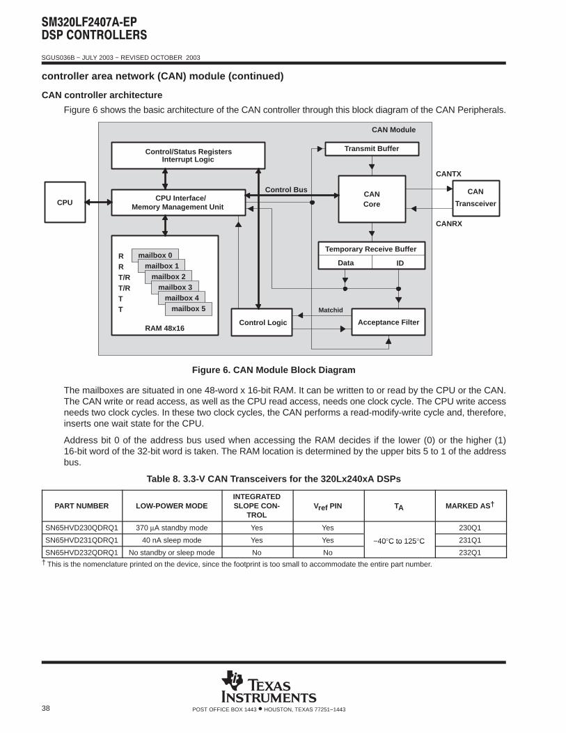
SGUS036B − JULY 2003 − REVISED OCTOBER 2003
38 POST OFFICE BOX 1443 • HOUSTON, TEXAS 77251−1443
controller area network (CAN) module (continued)
CAN controller architecture
Figure 6 shows the basic architecture of the CAN controller through this block diagram of the CAN Peripherals.
Temporary Receive Buffer
Data ID
CAN Module
Control Logic
CPU Interface/Memory Management Unit
CANCore
Control/Status RegistersInterrupt Logic
Control Bus
Acceptance Filter
Transmit Buffer
RAM 48x16
CANTX
CAN
Transceiver
Matchid
CPU
mailbox 0mailbox 1
mailbox 2mailbox 3
mailbox 4mailbox 5
RRT/RT/RTT
CANRX
Figure 6. CAN Module Block Diagram
The mailboxes are situated in one 48-word x 16-bit RAM. It can be written to or read by the CPU or the CAN.The CAN write or read access, as well as the CPU read access, needs one clock cycle. The CPU write accessneeds two clock cycles. In these two clock cycles, the CAN performs a read-modify-write cycle and, therefore,inserts one wait state for the CPU.
Address bit 0 of the address bus used when accessing the RAM decides if the lower (0) or the higher (1)16-bit word of the 32-bit word is taken. The RAM location is determined by the upper bits 5 to 1 of the addressbus.
Table 8. 3.3-V CAN Transceivers for the 320Lx240xA DSPs
PART NUMBER LOW-POWER MODEINTEGRATEDSLOPE CON-
TROLVref PIN TA MARKED AS †
SN65HVD230QDRQ1 370 µA standby mode Yes Yes 230Q1
SN65HVD231QDRQ1 40 nA sleep mode Yes Yes −40°C to 125°C 231Q1
SN65HVD232QDRQ1 No standby or sleep mode No No
−40 C to 125 C
232Q1† This is the nomenclature printed on the device, since the footprint is too small to accommodate the entire part number.
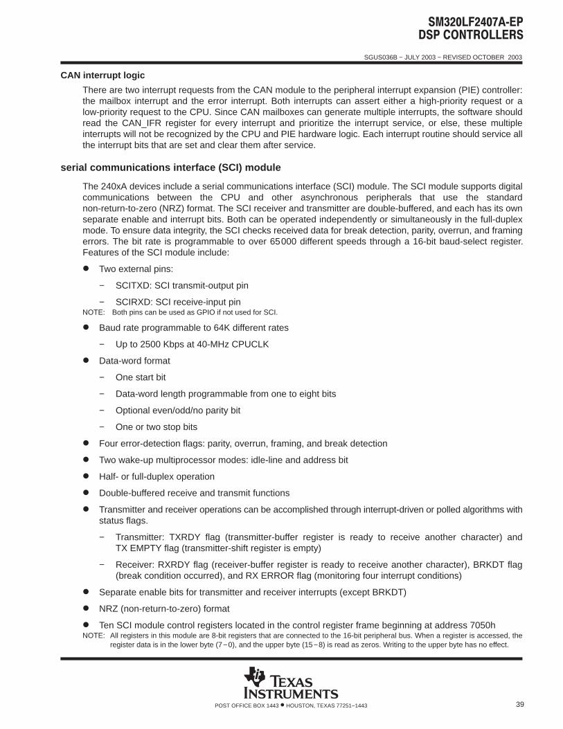
SGUS036B − JULY 2003 − REVISED OCTOBER 2003
39POST OFFICE BOX 1443 • HOUSTON, TEXAS 77251−1443
CAN interrupt logic
There are two interrupt requests from the CAN module to the peripheral interrupt expansion (PIE) controller:the mailbox interrupt and the error interrupt. Both interrupts can assert either a high-priority request or alow-priority request to the CPU. Since CAN mailboxes can generate multiple interrupts, the software shouldread the CAN_IFR register for every interrupt and prioritize the interrupt service, or else, these multipleinterrupts will not be recognized by the CPU and PIE hardware logic. Each interrupt routine should service allthe interrupt bits that are set and clear them after service.
serial communications interface (SCI) module
The 240xA devices include a serial communications interface (SCI) module. The SCI module supports digitalcommunications between the CPU and other asynchronous peripherals that use the standardnon-return-to-zero (NRZ) format. The SCI receiver and transmitter are double-buffered, and each has its ownseparate enable and interrupt bits. Both can be operated independently or simultaneously in the full-duplexmode. To ensure data integrity, the SCI checks received data for break detection, parity, overrun, and framingerrors. The bit rate is programmable to over 65000 different speeds through a 16-bit baud-select register.Features of the SCI module include:
Two external pins:
− SCITXD: SCI transmit-output pin
− SCIRXD: SCI receive-input pinNOTE: Both pins can be used as GPIO if not used for SCI.
Baud rate programmable to 64K different rates
− Up to 2500 Kbps at 40-MHz CPUCLK
Data-word format
− One start bit
− Data-word length programmable from one to eight bits
− Optional even/odd/no parity bit
− One or two stop bits
Four error-detection flags: parity, overrun, framing, and break detection
Two wake-up multiprocessor modes: idle-line and address bit
Half- or full-duplex operation
Double-buffered receive and transmit functions
Transmitter and receiver operations can be accomplished through interrupt-driven or polled algorithms withstatus flags.
− Transmitter: TXRDY flag (transmitter-buffer register is ready to receive another character) andTX EMPTY flag (transmitter-shift register is empty)
− Receiver: RXRDY flag (receiver-buffer register is ready to receive another character), BRKDT flag(break condition occurred), and RX ERROR flag (monitoring four interrupt conditions)
Separate enable bits for transmitter and receiver interrupts (except BRKDT)
NRZ (non-return-to-zero) format
Ten SCI module control registers located in the control register frame beginning at address 7050hNOTE: All registers in this module are 8-bit registers that are connected to the 16-bit peripheral bus. When a register is accessed, the
register data is in the lower byte (7−0), and the upper byte (15−8) is read as zeros. Writing to the upper byte has no effect.
SGUS036B − JULY 2003 − REVISED OCTOBER 2003
40 POST OFFICE BOX 1443 • HOUSTON, TEXAS 77251−1443
serial communications interface (SCI) module (continued)
Figure 7 shows the SCI module block diagram.
InternalClock
WUT
Frame Format and Mode
Even/Odd EnableParity
SCI RX Interrupt
BRKDT
SCICTL1.1
RXRDYSCIRXST.6
SCICTL1.3 ExternalConnections
8
SCICTL2.1
RX/BK INT ENA
SCIRXD
SCIRXST.1
TXENA
SCI TX Interrupt
TX EMPTY
TXRDY
SCICTL2.0
TX INT ENA
SCITXD
RXENA
SCIRXDRXWAKE
SCICTL1.0SCICTL1.6
RX ERR INT ENA
TXWAKE
SCITXD
TXINT
SCICCR.6 SCICCR.5
SCITXBUF.7−0
SCIHBAUD. 15−8
Baud RateMSbyteRegister
SCILBAUD. 7−0
SCIRXBUF.7−0
Receiver-DataBuffer
Register
SCIRXST.7
PEFE OE
RX Error
RX Error
SCIRXST.4−2
Transmitter-DataBuffer Register
8SCICTL2.6
SCICTL2.7
Baud RateLSbyte
Register
RXSHFRegister
TXSHF Register
SCIRXST.5 RX
INT
1
SCIPRI.5
SCIPRI.6
SCI Priority Level
Level 5 Int.
Level 1 Int.
Level 5 Int.
Level 1 Int.
1
0
1
0
SCI TXPriority
SCI RXPriority
Figure 7. Serial Communications Interface (SCI) Module Block Diagram
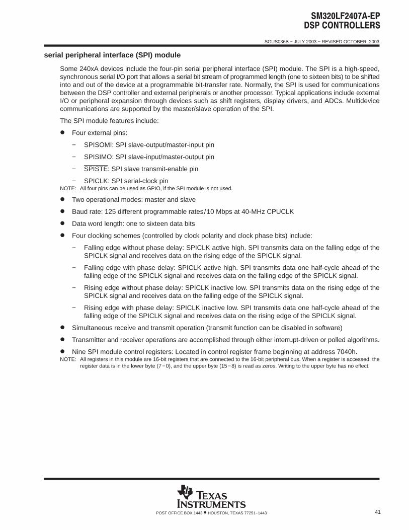
SGUS036B − JULY 2003 − REVISED OCTOBER 2003
41POST OFFICE BOX 1443 • HOUSTON, TEXAS 77251−1443
serial peripheral interface (SPI) module
Some 240xA devices include the four-pin serial peripheral interface (SPI) module. The SPI is a high-speed,synchronous serial I/O port that allows a serial bit stream of programmed length (one to sixteen bits) to be shiftedinto and out of the device at a programmable bit-transfer rate. Normally, the SPI is used for communicationsbetween the DSP controller and external peripherals or another processor. Typical applications include externalI/O or peripheral expansion through devices such as shift registers, display drivers, and ADCs. Multidevicecommunications are supported by the master/slave operation of the SPI.
The SPI module features include:
Four external pins:
− SPISOMI: SPI slave-output/master-input pin
− SPISIMO: SPI slave-input/master-output pin
− SPISTE: SPI slave transmit-enable pin
− SPICLK: SPI serial-clock pinNOTE: All four pins can be used as GPIO, if the SPI module is not used.
Two operational modes: master and slave
Baud rate: 125 different programmable rates/10 Mbps at 40-MHz CPUCLK
Data word length: one to sixteen data bits
Four clocking schemes (controlled by clock polarity and clock phase bits) include:
− Falling edge without phase delay: SPICLK active high. SPI transmits data on the falling edge of theSPICLK signal and receives data on the rising edge of the SPICLK signal.
− Falling edge with phase delay: SPICLK active high. SPI transmits data one half-cycle ahead of thefalling edge of the SPICLK signal and receives data on the falling edge of the SPICLK signal.
− Rising edge without phase delay: SPICLK inactive low. SPI transmits data on the rising edge of theSPICLK signal and receives data on the falling edge of the SPICLK signal.
− Rising edge with phase delay: SPICLK inactive low. SPI transmits data one half-cycle ahead of thefalling edge of the SPICLK signal and receives data on the rising edge of the SPICLK signal.
Simultaneous receive and transmit operation (transmit function can be disabled in software)
Transmitter and receiver operations are accomplished through either interrupt-driven or polled algorithms.
Nine SPI module control registers: Located in control register frame beginning at address 7040h.NOTE: All registers in this module are 16-bit registers that are connected to the 16-bit peripheral bus. When a register is accessed, the
register data is in the lower byte (7−0), and the upper byte (15−8) is read as zeros. Writing to the upper byte has no effect.
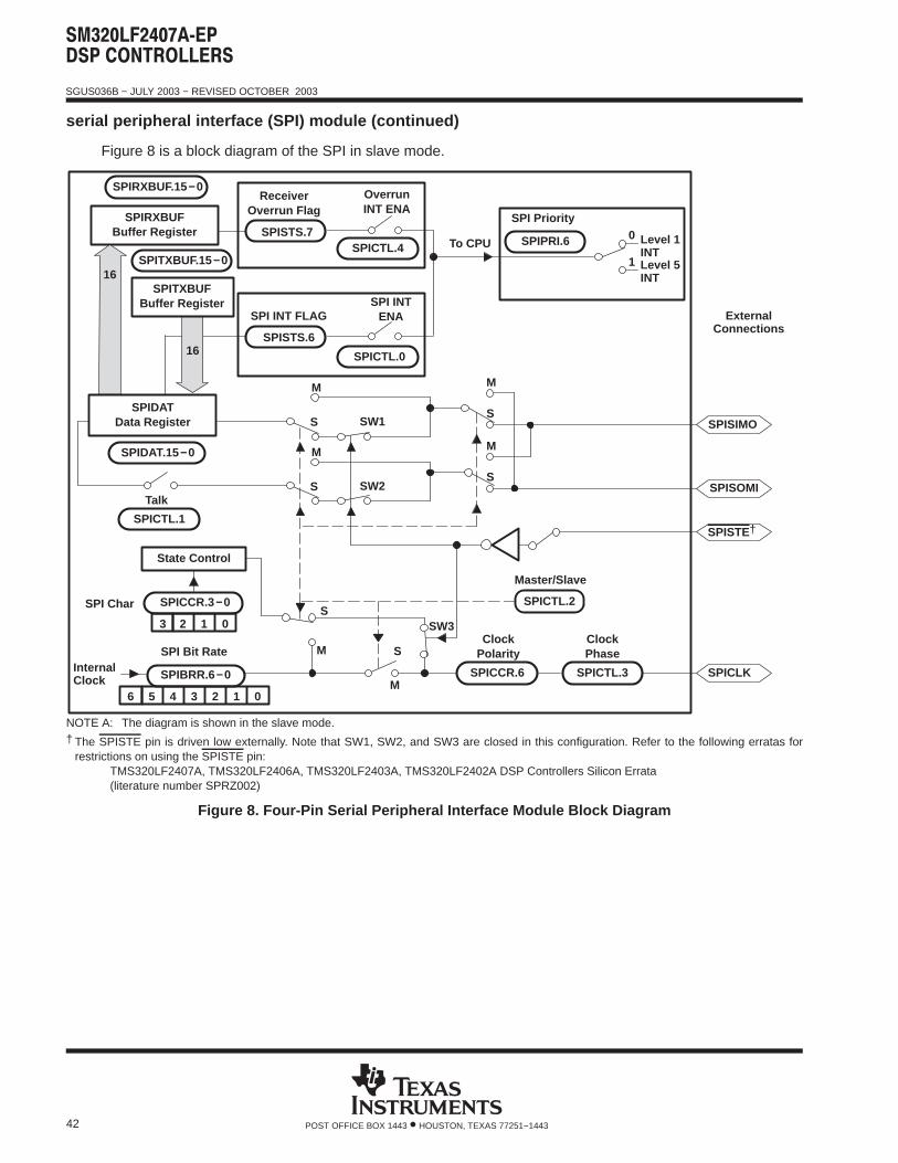
SGUS036B − JULY 2003 − REVISED OCTOBER 2003
42 POST OFFICE BOX 1443 • HOUSTON, TEXAS 77251−1443
serial peripheral interface (SPI) module (continued)
Figure 8 is a block diagram of the SPI in slave mode.
S
S
ClockPolarity
Talk
InternalClock
456
012
SPI Bit Rate
State Control
SPIRXBUFBuffer Register
16
ClockPhase
123 0
ReceiverOverrun Flag
SPICTL.4
OverrunINT ENA
SPICCR.3−0
SPIBRR.6−0 SPICCR.6 SPICTL.3
SPIRXBUF.15−0
SPIDAT.15−0
SPICTL.1
M
S
M
Master/Slave
SPI INT FLAG
SPICTL.0
SPI INTENA
SPISTS.7
SPIDATData Register
SPISTS.6
M
S
SPICTL.2SPI Char
ExternalConnections
SPISIMO
SPISOMI
SPISTE†
SPICLK
SW2
S
M
M
S
SW3
To CPU
M
SW1
SPIPRI.6
SPI Priority
Level 1INT
1
0
Level 5INT
SPITXBUF.15−0
3
16
SPITXBUFBuffer Register
NOTE A: The diagram is shown in the slave mode.† The SPISTE pin is driven low externally. Note that SW1, SW2, and SW3 are closed in this configuration. Refer to the following erratas for
restrictions on using the SPISTE pin:TMS320LF2407A, TMS320LF2406A, TMS320LF2403A, TMS320LF2402A DSP Controllers Silicon Errata(literature number SPRZ002)
Figure 8. Four-Pin Serial Peripheral Interface Module Block Diagram
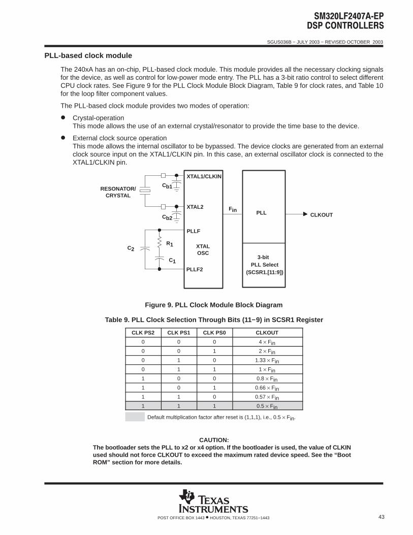
SGUS036B − JULY 2003 − REVISED OCTOBER 2003
43POST OFFICE BOX 1443 • HOUSTON, TEXAS 77251−1443
PLL-based clock module
The 240xA has an on-chip, PLL-based clock module. This module provides all the necessary clocking signalsfor the device, as well as control for low-power mode entry. The PLL has a 3-bit ratio control to select differentCPU clock rates. See Figure 9 for the PLL Clock Module Block Diagram, Table 9 for clock rates, and Table 10for the loop filter component values.
The PLL-based clock module provides two modes of operation:
Crystal-operationThis mode allows the use of an external crystal/resonator to provide the time base to the device.
External clock source operationThis mode allows the internal oscillator to be bypassed. The device clocks are generated from an externalclock source input on the XTAL1/CLKIN pin. In this case, an external oscillator clock is connected to theXTAL1/CLKIN pin.
XTAL2
XTAL1/CLKIN
PLL
XTALOSC
CLKOUTFin
3-bit PLL Select
(SCSR1.[11:9])
R1
C1
C2
PLLF
RESONATOR/CRYSTAL
PLLF2
Cb1
Cb2
Figure 9. PLL Clock Module Block Diagram
Table 9. PLL Clock Selection Through Bits (11−9) in SCSR1 Register
CLK PS2 CLK PS1 CLK PS0 CLKOUT
0 0 0 4 × Fin
0 0 1 2 × Fin
0 1 0 1.33 × Fin
0 1 1 1 × Fin
1 0 0 0.8 × Fin
1 0 1 0.66 × Fin
1 1 0 0.57 × Fin
1 1 1 0.5 × Fin
Default multiplication factor after reset is (1,1,1), i.e., 0.5 × Fin.
CAUTION:The bootloader sets the PLL to x2 or x4 option. If the bootloader is used, the value of CLKINused should not force CLKOUT to exceed the maximum rated device speed. See the “BootROM” section for more details.

SGUS036B − JULY 2003 − REVISED OCTOBER 2003
44 POST OFFICE BOX 1443 • HOUSTON, TEXAS 77251−1443
external reference crystal clock option
The internal oscillator is enabled by connecting a crystal across the XTAL1/CLKIN and XTAL2 pins as shownin Figure 10a. The crystal should be in fundamental operation and parallel resonant, with an effective seriesresistance of 30 Ω−150 Ω and a maximum power dissipation of 1 mW; it should be specified at a loadcapacitance of 20 pF.
external reference oscillator clock option
The internal oscillator is disabled by connecting a clock signal to XTAL1/CLKIN and leaving the XTAL2 inputpin unconnected as shown in Figure 10b.
External Clock Signal (Toggling 0−3.3 V)
Cb1(see Note A)
XTAL2XTAL1/CLKIN XTAL1/CLKIN XTAL2
CrystalCb2(see Note A)
(a) (b)
NC
NOTE A: TI recommends that customers have the resonator/crystal vendor characterize the operation of their device with the DSP chip. Theresonator/crystal vendor has the equipment and expertise to tune the tank circuit. The vendor can also advise the customer regardingthe proper tank component values that will ensure start-up and stability over the entire operating range.
Figure 10. Recommended Crystal /Clock Connection
loop filter
The PLL module uses an external loop filter circuit for jitter minimization. The components for the loop filtercircuit are R1, C1, and C2. The capacitors (C1 and C2) must be non-polarized. This loop filter circuit is connectedbetween the PLLF and PLLF2 pins (see Figure 9). For examples of component values of R1, C1, and C2 at aspecified oscillator frequency (XTAL1), see Table 10.
Table 10. Loop Filter Component Values With Damping Factor = 2.0
XTAL1/CLKIN FREQUENCY(MHz) R1 (Ω) (±5% TOLERANCE) C1 (µF) (±20% TOLERANCE) C2 (µF) (±20% TOLERANCE)
4 4.7 3.9 0.082
5 5.6 2.7 0.056
6 6.8 1.8 0.039
7 8.2 1.5 0.033
8 9.1 1 0.022
9 10 0.82 0.015
10 11 0.68 0.015
11 12 0.56 0.012
12 13 0.47 0.01
13 15 0.39 0.0082
14 15 0.33 0.0068
15 16 0.33 0.0068
16 18 0.27 0.0056
17 18 0.22 0.0047
18 20 0.22 0.0047
19 22 0.18 0.0039
20 24 0.15 0.0033
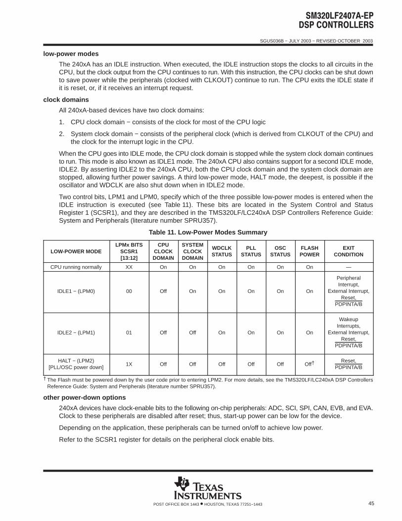
SGUS036B − JULY 2003 − REVISED OCTOBER 2003
45POST OFFICE BOX 1443 • HOUSTON, TEXAS 77251−1443
low-power modes
The 240xA has an IDLE instruction. When executed, the IDLE instruction stops the clocks to all circuits in theCPU, but the clock output from the CPU continues to run. With this instruction, the CPU clocks can be shut downto save power while the peripherals (clocked with CLKOUT) continue to run. The CPU exits the IDLE state ifit is reset, or, if it receives an interrupt request.
clock domains
All 240xA-based devices have two clock domains:
1. CPU clock domain − consists of the clock for most of the CPU logic
2. System clock domain − consists of the peripheral clock (which is derived from CLKOUT of the CPU) andthe clock for the interrupt logic in the CPU.
When the CPU goes into IDLE mode, the CPU clock domain is stopped while the system clock domain continuesto run. This mode is also known as IDLE1 mode. The 240xA CPU also contains support for a second IDLE mode,IDLE2. By asserting IDLE2 to the 240xA CPU, both the CPU clock domain and the system clock domain arestopped, allowing further power savings. A third low-power mode, HALT mode, the deepest, is possible if theoscillator and WDCLK are also shut down when in IDLE2 mode.
Two control bits, LPM1 and LPM0, specify which of the three possible low-power modes is entered when theIDLE instruction is executed (see Table 11). These bits are located in the System Control and StatusRegister 1 (SCSR1), and they are described in the TMS320LF/LC240xA DSP Controllers Reference Guide:System and Peripherals (literature number SPRU357).
Table 11. Low-Power Modes Summary
LOW-POWER MODELPMx BITS
SCSR1[13:12]
CPUCLOCKDOMAIN
SYSTEMCLOCKDOMAIN
WDCLKSTATUS
PLLSTATUS
OSCSTATUS
FLASHPOWER
EXITCONDITION
CPU running normally XX On On On On On On —
IDLE1 − (LPM0) 00 Off On On On On On
PeripheralInterrupt,
External Interrupt,Reset,
PDPINTA/B
IDLE2 − (LPM1) 01 Off Off On On On On
WakeupInterrupts,
External Interrupt,Reset,
PDPINTA/B
HALT − (LPM2)[PLL/OSC power down]
1X Off Off Off Off Off Off†Reset,
PDPINTA/B
† The Flash must be powered down by the user code prior to entering LPM2. For more details, see the TMS320LF/LC240xA DSP ControllersReference Guide: System and Peripherals (literature number SPRU357).
other power-down options
240xA devices have clock-enable bits to the following on-chip peripherals: ADC, SCI, SPI, CAN, EVB, and EVA.Clock to these peripherals are disabled after reset; thus, start-up power can be low for the device.
Depending on the application, these peripherals can be turned on/off to achieve low power.
Refer to the SCSR1 register for details on the peripheral clock enable bits.
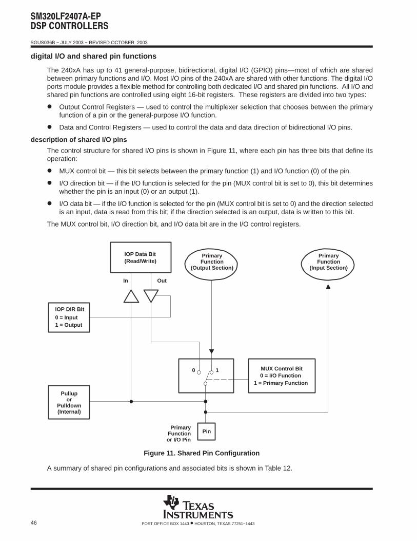
SGUS036B − JULY 2003 − REVISED OCTOBER 2003
46 POST OFFICE BOX 1443 • HOUSTON, TEXAS 77251−1443
digital I/O and shared pin functions
The 240xA has up to 41 general-purpose, bidirectional, digital I/O (GPIO) pins—most of which are sharedbetween primary functions and I/O. Most I/O pins of the 240xA are shared with other functions. The digital I/Oports module provides a flexible method for controlling both dedicated I/O and shared pin functions. All I/O andshared pin functions are controlled using eight 16-bit registers. These registers are divided into two types:
Output Control Registers — used to control the multiplexer selection that chooses between the primaryfunction of a pin or the general-purpose I/O function.
Data and Control Registers — used to control the data and data direction of bidirectional I/O pins.
description of shared I/O pins
The control structure for shared I/O pins is shown in Figure 11, where each pin has three bits that define itsoperation:
MUX control bit — this bit selects between the primary function (1) and I/O function (0) of the pin.
I/O direction bit — if the I/O function is selected for the pin (MUX control bit is set to 0), this bit determineswhether the pin is an input (0) or an output (1).
I/O data bit — if the I/O function is selected for the pin (MUX control bit is set to 0) and the direction selectedis an input, data is read from this bit; if the direction selected is an output, data is written to this bit.
The MUX control bit, I/O direction bit, and I/O data bit are in the I/O control registers.
Pin
(Read/Write)IOP Data Bit
In Out
0 = Input1 = Output
0 1 MUX Control Bit0 = I/O Function
1 = Primary Function
IOP DIR Bit
PrimaryFunctionor I/O Pin
Pullupor
Pulldown(Internal)
PrimaryFunction
(Output Section)
PrimaryFunction
(Input Section)
Figure 11. Shared Pin Configuration
A summary of shared pin configurations and associated bits is shown in Table 12.
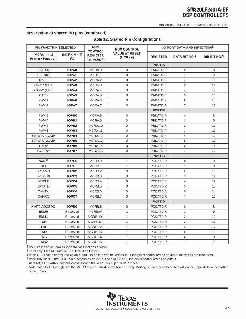
SGUS036B − JULY 2003 − REVISED OCTOBER 2003
47POST OFFICE BOX 1443 • HOUSTON, TEXAS 77251−1443
description of shared I/O pins (continued)
Table 12. Shared Pin Configurations †
PIN FUNCTION SELECTED MUXCONTROL
MUX CONTROL I/O PORT DATA AND DIRECTION ‡
(MCRx.n = 1)Primary Function
(MCRX.N = 0)I/O
CONTROLREGISTER(name.bit #)
MUX CONTROLVALUE AT RESET
(MCRx.n) REGISTER DATA BIT NO. § DIR BIT NO.¶
PORT A
SCITXD IOPA0 MCRA.0 0 PADATDIR 0 8
SCIRXD IOPA1 MCRA.1 0 PADATDIR 1 9
XINT1 IOPA2 MCRA.2 0 PADATDIR 2 10
CAP1/QEP1 IOPA3 MCRA.3 0 PADATDIR 3 11
CAP2/QEP2 IOPA4 MCRA.4 0 PADATDIR 4 12
CAP3 IOPA5 MCRA.5 0 PADATDIR 5 13
PWM1 IOPA6 MCRA.6 0 PADATDIR 6 14
PWM2 IOPA7 MCRA.7 0 PADATDIR 7 15
PORT B
PWM3 IOPB0 MCRA.8 0 PBDATDIR 0 8
PWM4 IOPB1 MCRA.9 0 PBDATDIR 1 9
PWM5 IOPB2 MCRA.10 0 PBDATDIR 2 10
PWM6 IOPB3 MCRA.11 0 PBDATDIR 3 11
T1PWM/T1CMP IOPB4 MCRA.12 0 PBDATDIR 4 12
T2PWM/T2CMP IOPB5 MCRA.13 0 PBDATDIR 5 13
TDIRA IOPB6 MCRA.14 0 PBDATDIR 6 14
TCLKINA IOPB7 MCRA.15 0 PBDATDIR 7 15
PORT C
W/R# IOPC0 MCRB.0 1 PCDATDIR 0 8
BIO IOPC1 MCRB.1 1 PCDATDIR 1 9
SPISIMO IOPC2 MCRB.2 0 PCDATDIR 2 10
SPISOMI IOPC3 MCRB.3 0 PCDATDIR 3 11
SPICLK IOPC4 MCRB.4 0 PCDATDIR 4 12
SPISTE IOPC5 MCRB.5 0 PCDATDIR 5 13
CANTX IOPC6 MCRB.6 0 PCDATDIR 6 14
CANRX IOPC7 MCRB.7 0 PCDATDIR 7 15
PORT D
XINT2/ADCSOC IOPD0 MCRB.8 0 PDDATDIR 0 8
EMU0 Reserved MCRB.9|| 1 PDDATDIR 1 9
EMU1 Reserved MCRB.10|| 1 PDDATDIR 2 10
TCK Reserved MCRB.11|| 1 PDDATDIR 3 11
TDI Reserved MCRB.12|| 1 PDDATDIR 4 12
TDO Reserved MCRB.13|| 1 PDDATDIR 5 13
TMS Reserved MCRB.14|| 1 PDDATDIR 6 14
TMS2 Reserved MCRB.15|| 1 PDDATDIR 7 15† Bold, italicized pin names indicate pin functions at reset.‡ Valid only if the I/O function is selected on the pin§ If the GPIO pin is configured as an output, these bits can be written to. If the pin is configured as an input, these bits are read from.¶ If the DIR bit is 0, the GPIO pin functions as an input. For a value of 1, the pin is configured as an output.# At reset, all LF240xA devices come up with the W/R/IOPC0 pin in W/R mode.|| Note that bits 15 through 9 of the MCRB register must be written as 1 only. Writing a 0 to any of these bits will cause unpredictable operation
of the device.
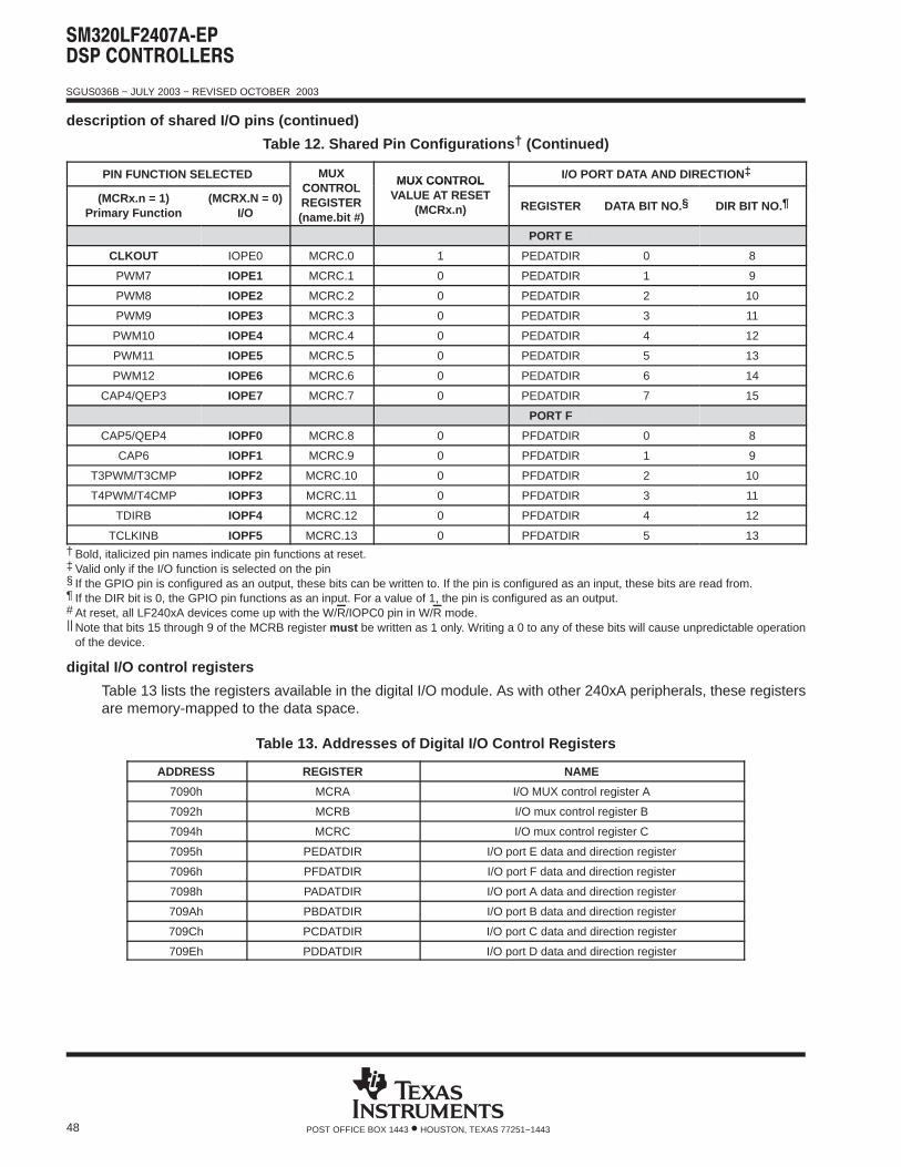
SGUS036B − JULY 2003 − REVISED OCTOBER 2003
48 POST OFFICE BOX 1443 • HOUSTON, TEXAS 77251−1443
description of shared I/O pins (continued)
Table 12. Shared Pin Configurations † (Continued)
PIN FUNCTION SELECTED MUXCONTROL
MUX CONTROL I/O PORT DATA AND DIRECTION ‡
(MCRx.n = 1)Primary Function
(MCRX.N = 0)I/O
CONTROLREGISTER(name.bit #)
MUX CONTROLVALUE AT RESET
(MCRx.n) REGISTER DATA BIT NO. § DIR BIT NO.¶
PORT E
CLKOUT IOPE0 MCRC.0 1 PEDATDIR 0 8
PWM7 IOPE1 MCRC.1 0 PEDATDIR 1 9
PWM8 IOPE2 MCRC.2 0 PEDATDIR 2 10
PWM9 IOPE3 MCRC.3 0 PEDATDIR 3 11
PWM10 IOPE4 MCRC.4 0 PEDATDIR 4 12
PWM11 IOPE5 MCRC.5 0 PEDATDIR 5 13
PWM12 IOPE6 MCRC.6 0 PEDATDIR 6 14
CAP4/QEP3 IOPE7 MCRC.7 0 PEDATDIR 7 15
PORT F
CAP5/QEP4 IOPF0 MCRC.8 0 PFDATDIR 0 8
CAP6 IOPF1 MCRC.9 0 PFDATDIR 1 9
T3PWM/T3CMP IOPF2 MCRC.10 0 PFDATDIR 2 10
T4PWM/T4CMP IOPF3 MCRC.11 0 PFDATDIR 3 11
TDIRB IOPF4 MCRC.12 0 PFDATDIR 4 12
TCLKINB IOPF5 MCRC.13 0 PFDATDIR 5 13† Bold, italicized pin names indicate pin functions at reset.‡ Valid only if the I/O function is selected on the pin§ If the GPIO pin is configured as an output, these bits can be written to. If the pin is configured as an input, these bits are read from.¶ If the DIR bit is 0, the GPIO pin functions as an input. For a value of 1, the pin is configured as an output.# At reset, all LF240xA devices come up with the W/R/IOPC0 pin in W/R mode.|| Note that bits 15 through 9 of the MCRB register must be written as 1 only. Writing a 0 to any of these bits will cause unpredictable operation
of the device.
digital I/O control registers
Table 13 lists the registers available in the digital I/O module. As with other 240xA peripherals, these registersare memory-mapped to the data space.
Table 13. Addresses of Digital I/O Control Registers
ADDRESS REGISTER NAME
7090h MCRA I/O MUX control register A
7092h MCRB I/O mux control register B
7094h MCRC I/O mux control register C
7095h PEDATDIR I/O port E data and direction register
7096h PFDATDIR I/O port F data and direction register
7098h PADATDIR I/O port A data and direction register
709Ah PBDATDIR I/O port B data and direction register
709Ch PCDATDIR I/O port C data and direction register
709Eh PDDATDIR I/O port D data and direction register

SGUS036B − JULY 2003 − REVISED OCTOBER 2003
49POST OFFICE BOX 1443 • HOUSTON, TEXAS 77251−1443
external memory interface (LF2407A)
The LF2407A can address up to 64K × 16 words of memory (or registers) in each of the program, data, and I/Ospaces. On-chip memory, when enabled, occupies some of this off-chip range.
The CPU of the LF2407A schedules a program fetch, data read, and data write on the same machine cycle.This is because from on-chip memory, the CPU can execute all three of these operations in the same cycle.However, the external interface multiplexes the internal buses to one address bus and one data bus. Theexternal interface sequences these operations to complete first the data write, then the data read, and finallythe program read.
The LF2407A supports a wide range of system interfacing requirements. Program, data, and I/O addressspaces provide interface to memory and I/O, thereby maximizing system throughput. The full 16-bit addressand data buses, along with the PS, DS, and IS space-select signals, allow addressing of 64K 16-bit words inprogram, data, and I/O space. Since on-chip peripheral registers occupy positions of data-memory space(7000−7FFF), the externally addressable data-memory space is 32K 16-bit words (8000−FFFF). Note that theglobal memory space of the C2xx core is not used for 240xA DSP devices. Therefore, the global memoryallocation register (GREG) is reserved for all these devices.
Input/output (I/O) design is simplified by having I/O space treated the same way as memory. I/O devices areaccessed in the I/O address space using the processor’s external address and data buses in the same manneras memory-mapped devices.
The LF2407A external parallel interface provides various control signals to facilitate interfacing to the device.The R/W output signal is provided to indicate whether the current cycle is a read or a write. The STRB outputsignal provides a timing reference for all external cycles. For convenience, the device also provides the RD andthe WE output signals, which indicate a read cycle and a write cycle, respectively, along with timing informationfor those cycles. The availability of these signals minimizes external gating necessary for interfacing externaldevices to the LF2407A.
The 2407A provides RD and W/R signals to help the zero-wait-state external memory interface. At higherCLKOUT speeds, RD may not meet the slow memory device’s timing. In such instances, the W/R signal couldbe used as an alternative signal with some tradeoffs. See the timings for details.
The LF2407A supports zero-wait-state reads on the external interface. However, to avoid bus conflicts, writestake two cycles. This allows the LF2407A to buffer the transition of the data bus from input to output (or fromoutput to input) by a half cycle. In most systems, the LF2407A ratio of reads to writes is significantly large tominimize the overhead of the extra cycle on writes.
wait-state generation
Wait-state generation is incorporated in the LF2407A without any external hardware for interfacing the LF2407Awith slower off-chip memory and I/O devices. Adding wait states lengthens the time the CPU waits for externalmemory or an external I/O port to respond when the CPU reads from or writes to that external memory or I/Oport. Specifically, the CPU waits one extra cycle (one CLKOUT cycle) for every wait state. The wait statesoperate on CLKOUT cycle boundaries.
To avoid bus conflicts, writes from the LF2407A always take at least two CLKOUT cycles. The LF2407A offerstwo options for generating wait states:
READY Signal. With the READY signal, you can externally generate any number of wait states. The READYpin has no effect on accesses to internal memory.
On-Chip Wait-State Generator. With this generator, you can generate zero to seven wait states.
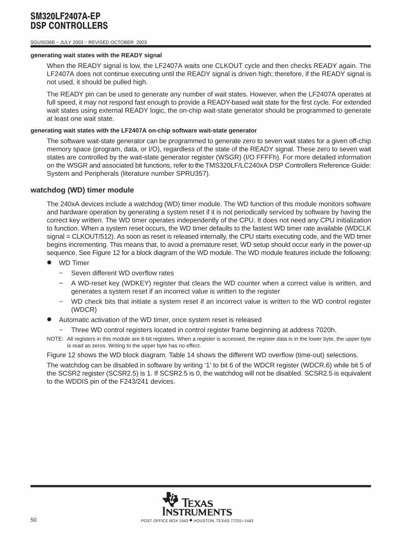
SGUS036B − JULY 2003 − REVISED OCTOBER 2003
50 POST OFFICE BOX 1443 • HOUSTON, TEXAS 77251−1443
generating wait states with the READY signal
When the READY signal is low, the LF2407A waits one CLKOUT cycle and then checks READY again. TheLF2407A does not continue executing until the READY signal is driven high; therefore, if the READY signal isnot used, it should be pulled high.
The READY pin can be used to generate any number of wait states. However, when the LF2407A operates atfull speed, it may not respond fast enough to provide a READY-based wait state for the first cycle. For extendedwait states using external READY logic, the on-chip wait-state generator should be programmed to generateat least one wait state.
generating wait states with the LF2407A on-chip software wait-state generator
The software wait-state generator can be programmed to generate zero to seven wait states for a given off-chipmemory space (program, data, or I/O), regardless of the state of the READY signal. These zero to seven waitstates are controlled by the wait-state generator register (WSGR) (I/O FFFFh). For more detailed informationon the WSGR and associated bit functions, refer to the TMS320LF/LC240xA DSP Controllers Reference Guide:System and Peripherals (literature number SPRU357).
watchdog (WD) timer module
The 240xA devices include a watchdog (WD) timer module. The WD function of this module monitors softwareand hardware operation by generating a system reset if it is not periodically serviced by software by having thecorrect key written. The WD timer operates independently of the CPU. It does not need any CPU initializationto function. When a system reset occurs, the WD timer defaults to the fastest WD timer rate available (WDCLKsignal = CLKOUT/512). As soon as reset is released internally, the CPU starts executing code, and the WD timerbegins incrementing. This means that, to avoid a premature reset, WD setup should occur early in the power-upsequence. See Figure 12 for a block diagram of the WD module. The WD module features include the following:
WD Timer
− Seven different WD overflow rates
− A WD-reset key (WDKEY) register that clears the WD counter when a correct value is written, andgenerates a system reset if an incorrect value is written to the register
− WD check bits that initiate a system reset if an incorrect value is written to the WD control register(WDCR)
Automatic activation of the WD timer, once system reset is released
− Three WD control registers located in control register frame beginning at address 7020h.NOTE: All registers in this module are 8-bit registers. When a register is accessed, the register data is in the lower byte, the upper byte
is read as zeros. Writing to the upper byte has no effect.
Figure 12 shows the WD block diagram. Table 14 shows the different WD overflow (time-out) selections.
The watchdog can be disabled in software by writing ‘1’ to bit 6 of the WDCR register (WDCR.6) while bit 5 ofthe SCSR2 register (SCSR2.5) is 1. If SCSR2.5 is 0, the watchdog will not be disabled. SCSR2.5 is equivalentto the WDDIS pin of the F243/241 devices.
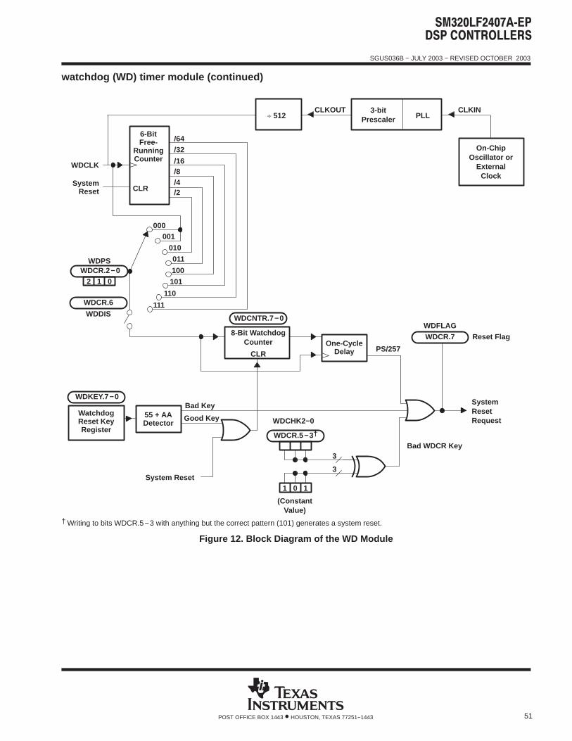
SGUS036B − JULY 2003 − REVISED OCTOBER 2003
51POST OFFICE BOX 1443 • HOUSTON, TEXAS 77251−1443
watchdog (WD) timer module (continued)
55 + AADetector
SystemResetRequest
WDCNTR.7−0
6-BitFree-
RunningCounter
/64/32
/16/8/4/2
111
110
101
100
011
010
001000
WDCLK
SystemReset
System Reset
CLR
One-CycleDelay
WatchdogReset KeyRegister
8-Bit WatchdogCounter
CLR
Bad WDCR Key
Good Key
Bad Key
WDPSWDCR.2−0
2 1 0
WDKEY.7−0
WDCHK2−0
WDCR.5−3†
WDCR.7WDFLAG
Reset Flag
PS/257
WDDIS
WDCR.6
1 0 1
(ConstantValue)
3
3
On-ChipOscillator or
ExternalClock
÷ 512 PLLCLKOUT CLKIN3-bit
Prescaler
† Writing to bits WDCR.5−3 with anything but the correct pattern (101) generates a system reset.
Figure 12. Block Diagram of the WD Module
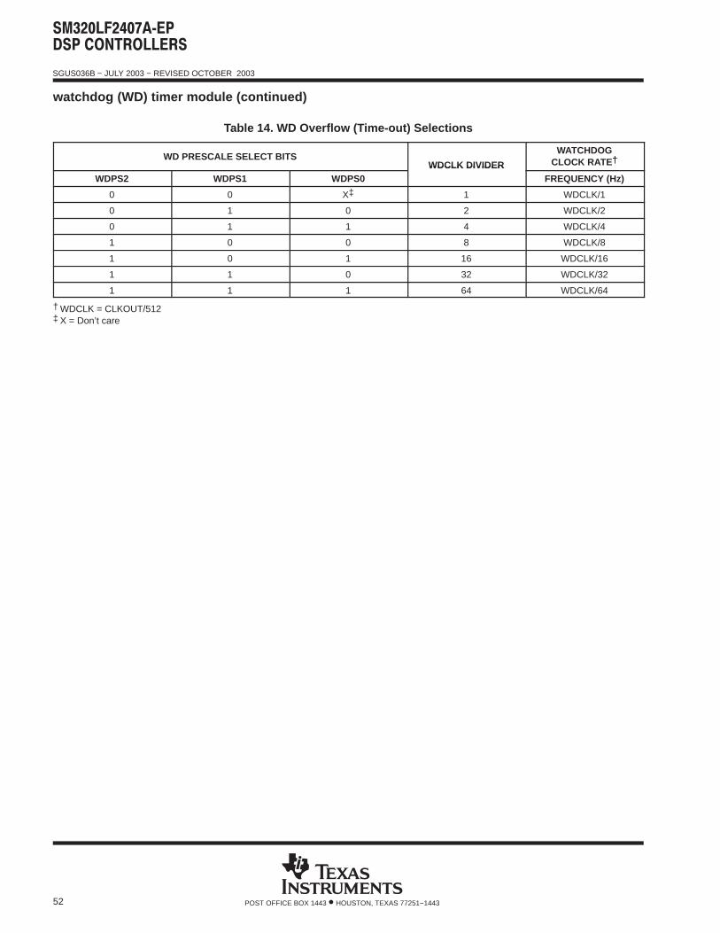
SGUS036B − JULY 2003 − REVISED OCTOBER 2003
52 POST OFFICE BOX 1443 • HOUSTON, TEXAS 77251−1443
watchdog (WD) timer module (continued)
Table 14. WD Overflow (Time-out) Selections
WD PRESCALE SELECT BITSWDCLK DIVIDER
WATCHDOGCLOCK RATE †
WDPS2 WDPS1 WDPS0WDCLK DIVIDER
FREQUENCY (Hz)
0 0 X‡ 1 WDCLK/1
0 1 0 2 WDCLK/2
0 1 1 4 WDCLK/4
1 0 0 8 WDCLK/8
1 0 1 16 WDCLK/16
1 1 0 32 WDCLK/32
1 1 1 64 WDCLK/64
† WDCLK = CLKOUT/512‡ X = Don’t care
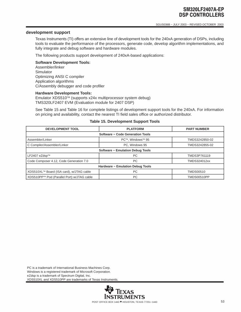
SGUS036B − JULY 2003 − REVISED OCTOBER 2003
53POST OFFICE BOX 1443 • HOUSTON, TEXAS 77251−1443
development supportTexas Instruments (TI) offers an extensive line of development tools for the 240xA generation of DSPs, includingtools to evaluate the performance of the processors, generate code, develop algorithm implementations, andfully integrate and debug software and hardware modules.
The following products support development of 240xA-based applications:
Software Development Tools:Assembler/linkerSimulatorOptimizing ANSI C compilerApplication algorithmsC/Assembly debugger and code profiler
Hardware Development Tools:Emulator XDS510 (supports x24x multiprocessor system debug)TMS320LF2407 EVM (Evaluation module for 2407 DSP)
See Table 15 and Table 16 for complete listings of development support tools for the 240xA. For informationon pricing and availability, contact the nearest TI field sales office or authorized distributor.
Table 15. Development Support Tools
DEVELOPMENT TOOL PLATFORM PART NUMBER
Software − Code Generation Tools
Assembler/Linker PC, Windows 95 TMDS3242850-02
C Compiler/Assembler/Linker PC, Windows 95 TMDS3242855-02
Software − Emulation Debug Tools
LF2407 eZdsp PC TMDS3P761119
Code Composer 4.12, Code Generation 7.0 PC TMDS324012xx
Hardware − Emulation Debug Tools
XDS510XL Board (ISA card), w/JTAG cable PC TMDS00510
XDS510PP Pod (Parallel Port) w/JTAG cable PC TMDS00510PP
PC is a trademark of International Business Machines Corp.Windows is a registered trademark of Microsoft Corporation.eZdsp is a trademark of Spectrum Digital, Inc.XDS510XL and XDS510PP are trademarks of Texas Instruments.
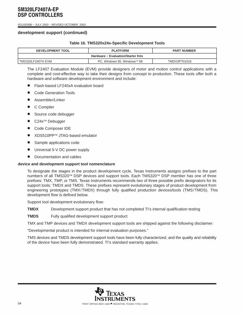
SGUS036B − JULY 2003 − REVISED OCTOBER 2003
54 POST OFFICE BOX 1443 • HOUSTON, TEXAS 77251−1443
development support (continued)
Table 16. TMS320x24x-Specific Development Tools
DEVELOPMENT TOOL PLATFORM PART NUMBER
Hardware − Evaluation/Starter Kits
TMS320LF2407A EVM PC, Windows 95, Windows 98 TMDX3P701016
The LF2407 Evaluation Module (EVM) provide designers of motor and motion control applications with acomplete and cost-effective way to take their designs from concept to production. These tools offer both ahardware and software development environment and include:
Flash-based LF240xA evaluation board
Code Generation Tools
Assembler/Linker
C Compiler
Source code debugger
C24x Debugger
Code Composer IDE
XDS510PP JTAG-based emulator
Sample applications code
Universal 5-V DC power supply
Documentation and cables
device and development support tool nomenclature
To designate the stages in the product development cycle, Texas Instruments assigns prefixes to the partnumbers of all TMS320 DSP devices and support tools. Each TMS320 DSP member has one of threeprefixes: TMX, TMP, or TMS. Texas Instruments recommends two of three possible prefix designators for itssupport tools: TMDX and TMDS. These prefixes represent evolutionary stages of product development fromengineering prototypes (TMX/TMDX) through fully qualified production devices/tools (TMS/TMDS). Thisdevelopment flow is defined below.
Support tool development evolutionary flow:
TMDX Development support product that has not completed TI’s internal qualification testing
TMDS Fully qualified development support product
TMX and TMP devices and TMDX development support tools are shipped against the following disclaimer:
“Developmental product is intended for internal evaluation purposes.”
TMS devices and TMDS development support tools have been fully characterized, and the quality and reliabilityof the device have been fully demonstrated. TI’s standard warranty applies.
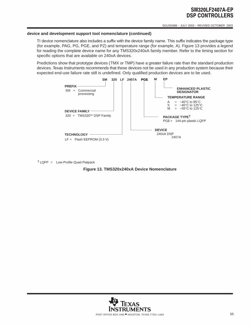
SGUS036B − JULY 2003 − REVISED OCTOBER 2003
55POST OFFICE BOX 1443 • HOUSTON, TEXAS 77251−1443
device and development support tool nomenclature (continued)
TI device nomenclature also includes a suffix with the device family name. This suffix indicates the package type(for example, PAG, PG, PGE, and PZ) and temperature range (for example, A). Figure 13 provides a legendfor reading the complete device name for any TMS320x240xA family member. Refer to the timing section forspecific options that are available on 240xA devices.
Predictions show that prototype devices (TMX or TMP) have a greater failure rate than the standard productiondevices. Texas Instruments recommends that these devices not be used in any production system because theirexpected end-use failure rate still is undefined. Only qualified production devices are to be used.
PREFIX
SM 320 LF 2407A PGE
SM = Commercial processing
DEVICE FAMILY320 = TMS320 DSP Family
TECHNOLOGY
PACKAGE TYPE †PGE= 144-pin plastic LQFP
LF = Flash EEPROM (3.3 V)
DEVICE240xA DSP
2407A
† LQFP = Low-Profile Quad Flatpack
TEMPERATURE RANGEA = −40°C to 85°CS = −40°C to 125°CM = −55°C to 125°C
PGE M EP
ENHANCED PLASTICDESIGNATOR
Figure 13. TMS320x240xA Device Nomenclature
SGUS036B − JULY 2003 − REVISED OCTOBER 2003
56 POST OFFICE BOX 1443 • HOUSTON, TEXAS 77251−1443
documentation support
Extensive documentation supports all of the TMS320 DSP family generations of devices from productannouncement through applications development. The types of documentation available include: data sheets,such as this document, with design specifications; complete user’s guides for all devices and developmentsupport tools; and hardware and software applications. Useful reference documentation includes:
User Guides
− TMS320LF/LC240xA DSP Controllers Reference Guide: System and Peripherals (literature numberSPRU357)
− Manual Update Sheet for TMS320LF/LC240xA DSP Controllers Reference Guide: System andPeripherals (SPRU357B) [literature number SPRZ015]
− TMS320C240 DSP Controllers CPU, System, and Instruction Set Reference Guide(literature number SPRU160)
Data Sheets
− TMS320LF2407A, TMS320LF2406A, TMS320LF2403A, TMS320LF2402A, TMS320LC2406A,TMS320LC2404A, TMS320LC2402A DSP Controllers (literature number SPRS145)
− TMS320LF2407, TMS320LF2406, TMS320LF2402 DSP Controllers (literature number SPRS094)
− TMS320LF2401A DSP Controller (literature number SPRS161)
Application Reports
− 3.3V DSP for Digital Motor Control (literature number SPRA550)
To receive copies of TMS320 DSP literature, contact the Literature Response Center at 800-477-8924.
A series of DSP textbooks is published by Prentice-Hall and John Wiley & Sons to support digital signalprocessing research and education. The TMS320 DSP newsletter, Details on Signal Processing, is publishedquarterly and distributed to update TMS320 DSP customers on product information.
Updated information on the TMS320 DSP controllers can be found on the worldwide web at:http://www.ti.com .
To send comments regarding this TMS320x240xA data sheet (literature number SPRS145), use [email protected] email address, which is a repository for feedback. For questions and support,contact the Product Information Center listed at the http://www.ti.com/sc/docs/pic/home.htm site.
SGUS036B − JULY 2003 − REVISED OCTOBER 2003
57POST OFFICE BOX 1443 • HOUSTON, TEXAS 77251−1443
LF240xA ELECTRICAL SPECIFICATIONS DATA
absolute maximum ratings over operating case temperature ranges (unless otherwise noted) †
Supply voltage range, VDD, PLLVCCA, VDDO, and VCCA (see Note 1) − 0.3 V to 4.6 V. . . . . . . . . . . . . . . . . . VCCP range − 0.3 V to 5.5 V. . . . . . . . . . . . . . . . . . . . . . . . . . . . . . . . . . . . . . . . . . . . . . . . . . . . . . . . . . . . . . . . . . . . . Input voltage range, VIN − 0.3 V to 4.6 V. . . . . . . . . . . . . . . . . . . . . . . . . . . . . . . . . . . . . . . . . . . . . . . . . . . . . . . . . . Output voltage range, VO − 0.3 V to 4.6 V. . . . . . . . . . . . . . . . . . . . . . . . . . . . . . . . . . . . . . . . . . . . . . . . . . . . . . . . . Input clamp current, IIK (VIN < 0 or VIN > VCC) ± 20 mA. . . . . . . . . . . . . . . . . . . . . . . . . . . . . . . . . . . . . . . . . . . . . Output clamp current, IOK (VO < 0 or VO > VCC) ± 20 mA. . . . . . . . . . . . . . . . . . . . . . . . . . . . . . . . . . . . . . . . . . . . Operating case temperature ranges, TC: M version (see Notes 2 and 3) − 55°C to 125°C. . . . . . . . . . . . . Junction temperature range, TJ (see Note 3) − 55°C to 130°C. . . . . . . . . . . . . . . . . . . . . . . . . . . . . . . . . . . . . . . Storage temperature range, Tstg (see Note 2) − 65°C to 150°C. . . . . . . . . . . . . . . . . . . . . . . . . . . . . . . . . . . . . .
† Clamp current stresses beyond those listed under “absolute maximum ratings” may cause permanent damage to the device. These are stressratings only, and functional operation of the device at these or any other conditions beyond those indicated under “recommended operatingconditions” is not implied. Exposure to absolute-maximum-rated conditions for extended periods may affect device reliability.
NOTES: 1. All voltage values are with respect to VSS.2. Long term high−temperature storage and/or extended use at maximum recommended operating conditions may result in a reduction
of overall device life. See http://www.ti.com/ep_quality for additional information on enhanced plastic packaging.3. See the next section on device operating life for important information on temperature ranges.
device operating life
125°C case operating temperature denotes maximum test temperature only. Impact on estimated product lifefrom continuous operation of this device at elevated temperatures are shown in Figure 14 .
Bond (package) life is based on time-to-first failure due to intermetallic formation. After the first failure isencountered, the failure rate approaches 100% in a very short time (a matter of months) due to the nature ofthe failure mechanism.
Since the bond intermetallic life is a function of package components and temperature only, the 150°C point isincluded to indicate the effect of extended high temperature storage.
Electromigration life is based on a FR50 of 50 FITS with an activation energy of 0.75 eV and follows a standardwear-out curve.
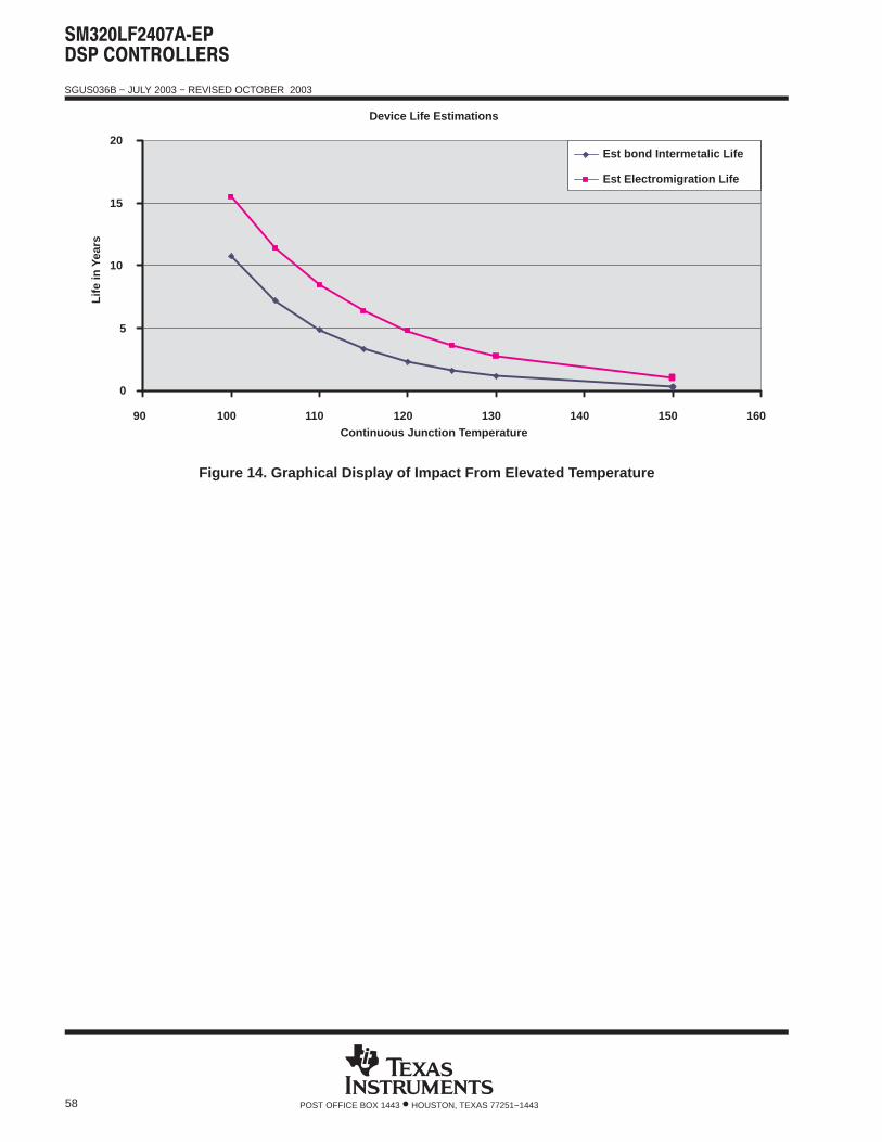
SGUS036B − JULY 2003 − REVISED OCTOBER 2003
58 POST OFFICE BOX 1443 • HOUSTON, TEXAS 77251−1443
Device Life Estimations
0
5
10
15
20
90 100 110 120 130 140 150 160Continuous Junction Temperature
Life
in Y
ears
Est bond Intermetalic Life
Est Electromigration Life
Figure 14. Graphical Display of Impact From Elevated Temperature
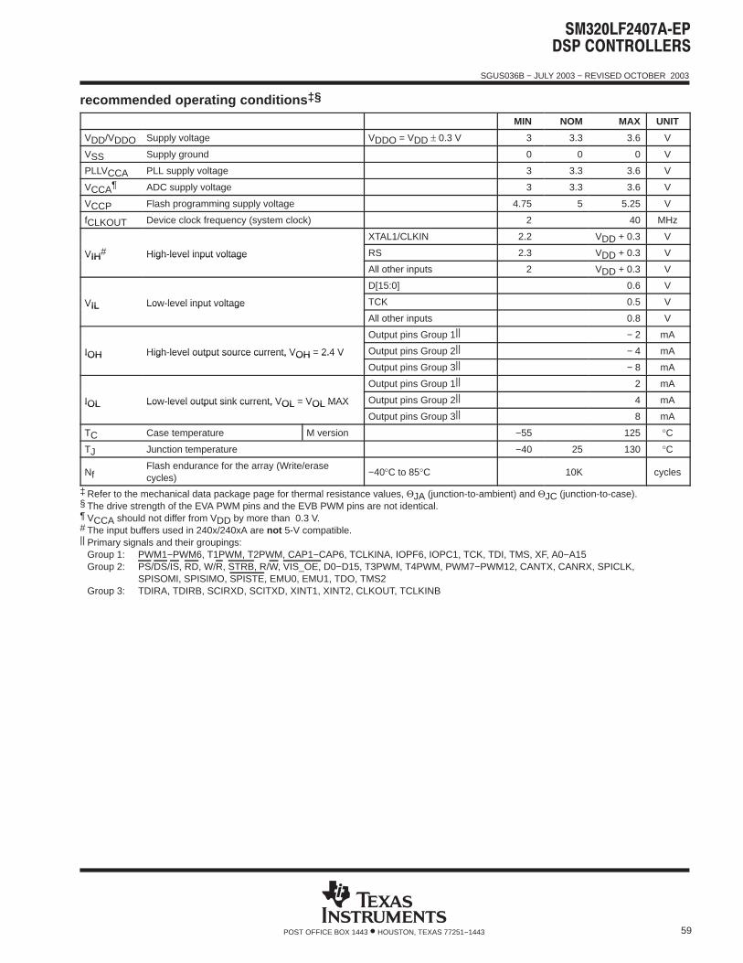
SGUS036B − JULY 2003 − REVISED OCTOBER 2003
59POST OFFICE BOX 1443 • HOUSTON, TEXAS 77251−1443
recommended operating conditions ‡§
MIN NOM MAX UNIT
VDD/VDDO Supply voltage VDDO = VDD ± 0.3 V 3 3.3 3.6 V
VSS Supply ground 0 0 0 V
PLLVCCA PLL supply voltage 3 3.3 3.6 V
VCCA¶ ADC supply voltage 3 3.3 3.6 V
VCCP Flash programming supply voltage 4.75 5 5.25 V
fCLKOUT Device clock frequency (system clock) 2 40 MHz
XTAL1/CLKIN 2.2 VDD + 0.3 V
VIH# High-level input voltage RS 2.3 VDD + 0.3 VVIH# High-level input voltage
All other inputs 2 VDD + 0.3 V
D[15:0] 0.6 V
VIL Low-level input voltage TCK 0.5 VVIL Low-level input voltage
All other inputs 0.8 V
Output pins Group 1|| − 2 mA
IOH High-level output source current, VOH = 2.4 V Output pins Group 2|| − 4 mAIOH High-level output source current, VOH = 2.4 V
Output pins Group 3|| − 8 mA
Output pins Group 1|| 2 mA
IOL Low-level output sink current, VOL = VOL MAX Output pins Group 2|| 4 mAIOL Low-level output sink current, VOL = VOL MAX
Output pins Group 3|| 8 mA
TC Case temperature M version −55 125 °C
TJ Junction temperature −40 25 130 °C
NfFlash endurance for the array (Write/erasecycles)
−40°C to 85°C 10K cycles
‡ Refer to the mechanical data package page for thermal resistance values, ΘJA (junction-to-ambient) and ΘJC (junction-to-case).§ The drive strength of the EVA PWM pins and the EVB PWM pins are not identical.¶ VCCA should not differ from VDD by more than 0.3 V.# The input buffers used in 240x/240xA are not 5-V compatible.|| Primary signals and their groupings:
Group 1: PWM1−PWM6, T1PWM, T2PWM, CAP1−CAP6, TCLKINA, IOPF6, IOPC1, TCK, TDI, TMS, XF, A0−A15Group 2: PS/DS/IS, RD, W/R, STRB, R/W, VIS_OE, D0−D15, T3PWM, T4PWM, PWM7−PWM12, CANTX, CANRX, SPICLK,
SPISOMI, SPISIMO, SPISTE, EMU0, EMU1, TDO, TMS2Group 3: TDIRA, TDIRB, SCIRXD, SCITXD, XINT1, XINT2, CLKOUT, TCLKINB
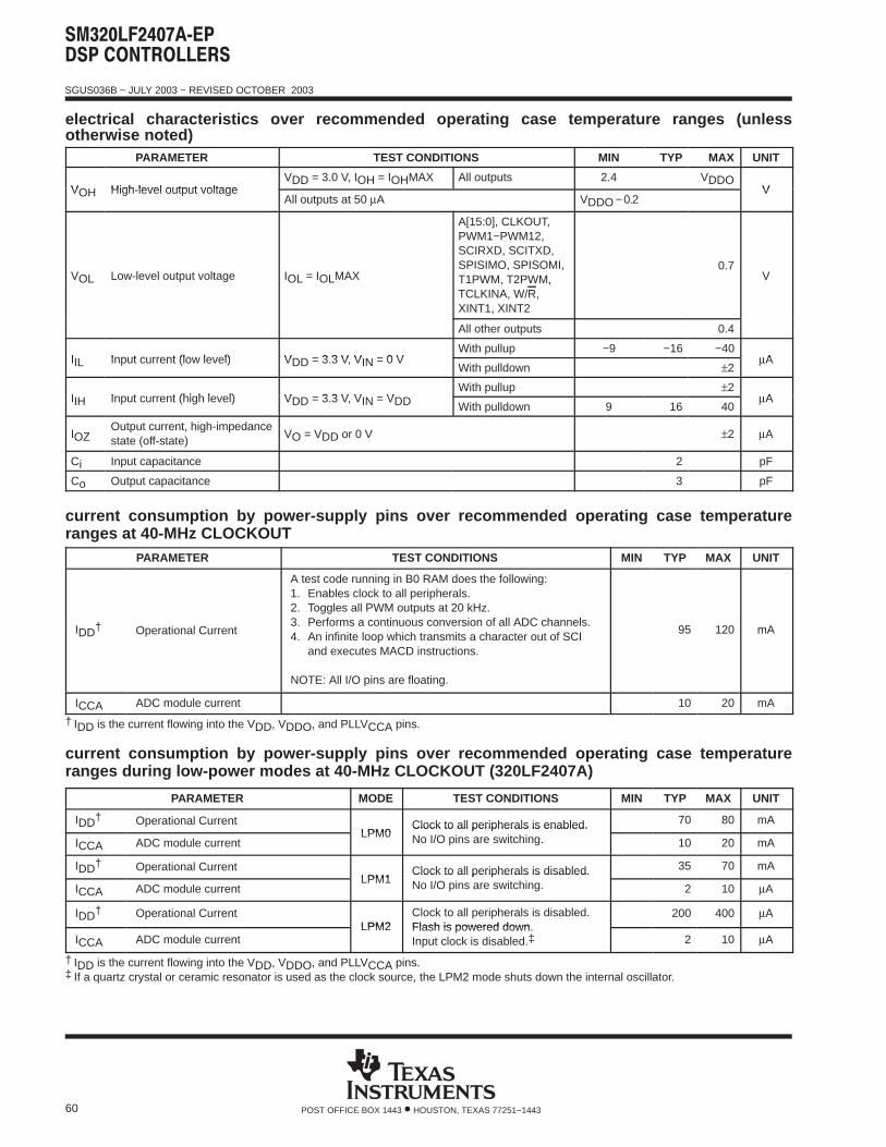
SGUS036B − JULY 2003 − REVISED OCTOBER 2003
60 POST OFFICE BOX 1443 • HOUSTON, TEXAS 77251−1443
electrical characteristics over recommended operating case temperature ranges (unlessotherwise noted)
PARAMETER TEST CONDITIONS MIN TYP MAX UNIT
VOH High-level output voltageVDD = 3.0 V, IOH = IOHMAX All outputs 2.4 VDDO
VVOH High-level output voltageAll outputs at 50 µA VDDO − 0.2
V
VOL Low-level output voltage IOL = IOLMAX
A[15:0], CLKOUT,PWM1−PWM12,SCIRXD, SCITXD,SPISIMO, SPISOMI,T1PWM, T2PWM,TCLKINA, W/R,XINT1, XINT2
0.7V
All other outputs 0.4
IIL Input current (low level) VDD = 3.3 V, VIN = 0 VWith pullup −9 −16 −40
AIIL Input current (low level) VDD = 3.3 V, VIN = 0 VWith pulldown ±2
µA
IIH Input current (high level) VDD = 3.3 V, VIN = VDDWith pullup ±2
AIIH Input current (high level) VDD = 3.3 V, VIN = VDD With pulldown 9 16 40µA
IOZOutput current, high-impedancestate (off-state)
VO = VDD or 0 V ±2 µA
Ci Input capacitance 2 pF
Co Output capacitance 3 pF
current consumption by power-supply pins over recommended operating case temperatureranges at 40-MHz CLOCKOUT
PARAMETER TEST CONDITIONS MIN TYP MAX UNIT
IDD† Operational Current
A test code running in B0 RAM does the following:1. Enables clock to all peripherals.2. Toggles all PWM outputs at 20 kHz.3. Performs a continuous conversion of all ADC channels.4. An infinite loop which transmits a character out of SCI
and executes MACD instructions.
NOTE: All I/O pins are floating.
95 120 mA
ICCA ADC module current 10 20 mA
† IDD is the current flowing into the VDD, VDDO, and PLLVCCA pins.
current consumption by power-supply pins over recommended operating case temperatureranges during low-power modes at 40-MHz CLOCKOUT (320LF2407A)
PARAMETER MODE TEST CONDITIONS MIN TYP MAX UNIT
IDD† Operational CurrentLPM0
Clock to all peripherals is enabled.No I/O pins are switching.
70 80 mA
ICCA ADC module currentLPM0
Clock to all peripherals is enabled.No I/O pins are switching. 10 20 mA
IDD† Operational CurrentLPM1
Clock to all peripherals is disabled.No I/O pins are switching.
35 70 mA
ICCA ADC module currentLPM1
Clock to all peripherals is disabled.No I/O pins are switching. 2 10 µA
IDD† Operational CurrentLPM2
Clock to all peripherals is disabled.Flash is powered down.
200 400 µA
ICCA ADC module currentLPM2 Flash is powered down.
Input clock is disabled.‡ 2 10 µA
† IDD is the current flowing into the VDD, VDDO, and PLLVCCA pins.‡ If a quartz crystal or ceramic resonator is used as the clock source, the LPM2 mode shuts down the internal oscillator.
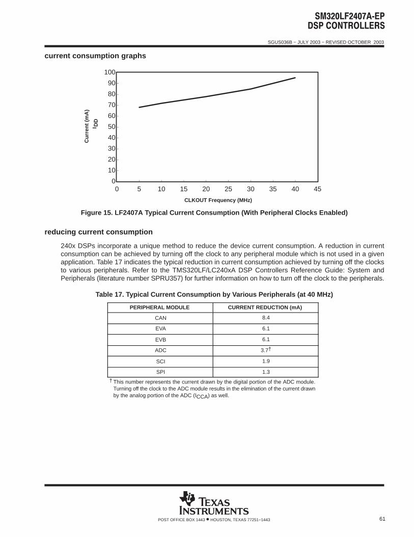
SGUS036B − JULY 2003 − REVISED OCTOBER 2003
61POST OFFICE BOX 1443 • HOUSTON, TEXAS 77251−1443
current consumption graphs
0
10
20
30
40
50
60
70
80
90
100
0 5 10 15 20 25 30 35 40 45
CLKOUT Frequency (MHz)
Cur
rent
(m
A)
I DD
Figure 15. LF2407A Typical Current Consumption (With Peripheral Clocks Enabled)
reducing current consumption
240x DSPs incorporate a unique method to reduce the device current consumption. A reduction in currentconsumption can be achieved by turning off the clock to any peripheral module which is not used in a givenapplication. Table 17 indicates the typical reduction in current consumption achieved by turning off the clocksto various peripherals. Refer to the TMS320LF/LC240xA DSP Controllers Reference Guide: System andPeripherals (literature number SPRU357) for further information on how to turn off the clock to the peripherals.
Table 17. Typical Current Consumption by Various Peripherals (at 40 MHz)
PERIPHERAL MODULE CURRENT REDUCTION (mA)
CAN 8.4
EVA 6.1
EVB 6.1
ADC 3.7†
SCI 1.9
SPI 1.3
† This number represents the current drawn by the digital portion of the ADC module.Turning off the clock to the ADC module results in the elimination of the current drawnby the analog portion of the ADC (ICCA) as well.
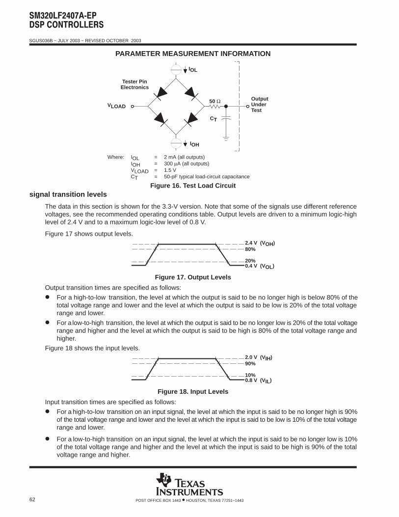
SGUS036B − JULY 2003 − REVISED OCTOBER 2003
62 POST OFFICE BOX 1443 • HOUSTON, TEXAS 77251−1443
PARAMETER MEASUREMENT INFORMATION
Tester PinElectronics
VLOAD
IOL
CT
IOH
OutputUnderTest
50 Ω
Where: IOL = 2 mA (all outputs)IOH = 300 µA (all outputs)VLOAD = 1.5 VCT = 50-pF typical load-circuit capacitance
Figure 16. Test Load Circuitsignal transition levels
The data in this section is shown for the 3.3-V version. Note that some of the signals use different referencevoltages, see the recommended operating conditions table. Output levels are driven to a minimum logic-highlevel of 2.4 V and to a maximum logic-low level of 0.8 V.
Figure 17 shows output levels.
0.4 V (VOL)20%
2.4 V (VOH)80%
Figure 17. Output Levels
Output transition times are specified as follows:
For a high-to-low transition, the level at which the output is said to be no longer high is below 80% of thetotal voltage range and lower and the level at which the output is said to be low is 20% of the total voltagerange and lower.
For a low-to-high transition, the level at which the output is said to be no longer low is 20% of the total voltagerange and higher and the level at which the output is said to be high is 80% of the total voltage range andhigher.
Figure 18 shows the input levels.
0.8 V (VIL)10%
2.0 V (VIH)90%
Figure 18. Input Levels
Input transition times are specified as follows:
For a high-to-low transition on an input signal, the level at which the input is said to be no longer high is 90%of the total voltage range and lower and the level at which the input is said to be low is 10% of the total voltagerange and lower.
For a low-to-high transition on an input signal, the level at which the input is said to be no longer low is 10%of the total voltage range and higher and the level at which the input is said to be high is 90% of the totalvoltage range and higher.

SGUS036B − JULY 2003 − REVISED OCTOBER 2003
63POST OFFICE BOX 1443 • HOUSTON, TEXAS 77251−1443
PARAMETER MEASUREMENT INFORMATION
timing parameter symbology
Timing parameter symbols used are created in accordance with JEDEC Standard 100. To shorten the symbols,some of the pin names and other related terminology have been abbreviated as follows:
A A[15:0] MS Memory strobe pins IS, DS, or PS
Cl XTAL1/CLKIN R READY
CO CLKOUT RD Read cycle or RD
D D[15:0] RS RESET pin RS
INT XINT1, XINT2 W Write cycle or WE
Lowercase subscripts and their meanings: Letters and symbols and their meanings:
a access time H High
c cycle time (period) L Low
d delay time V Valid
f fall time X Unknown, changing, or don’t care level
h hold time Z High impedance
r rise time
su setup time
t transition time
v valid time
w pulse duration (width)
general notes on timing parameters
All output signals from the 240xA devices (including CLKOUT) are derived from an internal clock such that alloutput transitions for a given half-cycle occur with a minimum of skewing relative to each other.
The signal combinations shown in the following timing diagrams may not necessarily represent actual cycles.For actual cycle examples, refer to the appropriate cycle description section of this data sheet.
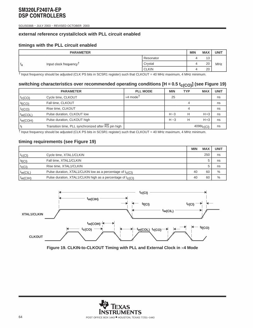
SGUS036B − JULY 2003 − REVISED OCTOBER 2003
64 POST OFFICE BOX 1443 • HOUSTON, TEXAS 77251−1443
external reference crystal/clock with PLL circuit enabled
timings with the PLL circuit enabled
PARAMETER MIN MAX UNIT
Resonator 4 13
fx Input clock frequency† Crystal 4 20 MHzfx Input clock frequency†
CLKIN 4 20
MHz
† Input frequency should be adjusted (CLK PS bits in SCSR1 register) such that CLKOUT = 40 MHz maximum, 4 MHz minimum.
switching characteristics over recommended operating conditions [H = 0.5 t c(CO)] (see Figure 19)
PARAMETER PLL MODE MIN TYP MAX UNIT
tc(CO) Cycle time, CLKOUT ×4 mode† 25 ns
tf(CO) Fall time, CLKOUT 4 ns
tr(CO) Rise time, CLKOUT 4 ns
tw(COL) Pulse duration, CLKOUT low H−3 H H+3 ns
tw(COH) Pulse duration, CLKOUT high H −3 H H+3 ns
tt Transition time, PLL synchronized after RS pin high 4096tc(Cl) ns
† Input frequency should be adjusted (CLK PS bits in SCSR1 register) such that CLKOUT = 40 MHz maximum, 4 MHz minimum.
timing requirements (see Figure 19)
MIN MAX UNIT
tc(Cl) Cycle time, XTAL1/CLKIN 250 ns
tf(Cl) Fall time, XTAL1/CLKIN 5 ns
tr(Cl) Rise time, XTAL1/CLKIN 5 ns
tw(CIL) Pulse duration, XTAL1/CLKIN low as a percentage of tc(Cl) 40 60 %
tw(CIH) Pulse duration, XTAL1/CLKIN high as a percentage of tc(Cl) 40 60 %
XTAL1/CLKIN
tc(CI)
tw(CIL)
tw(CIH)tf(Cl) tr(Cl)
tc(CO)
tw(COH)
tw(COL) tr(CO)tf(CO)
CLKOUT
Figure 19. CLKIN-to-CLKOUT Timing with PLL and External Clock in ×4 Mode
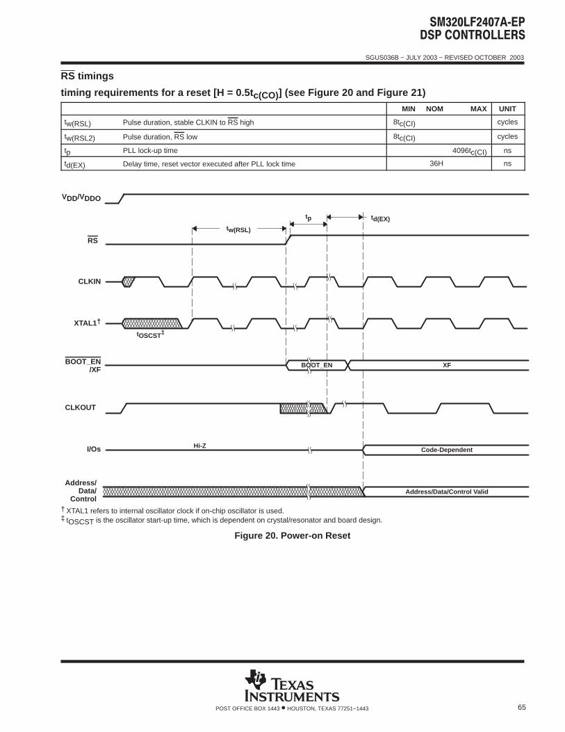
SGUS036B − JULY 2003 − REVISED OCTOBER 2003
65POST OFFICE BOX 1443 • HOUSTON, TEXAS 77251−1443
RS timings
timing requirements for a reset [H = 0.5t c(CO)] (see Figure 20 and Figure 21)
MIN NOM MAX UNIT
tw(RSL) Pulse duration, stable CLKIN to RS high 8tc(CI) cycles
tw(RSL2) Pulse duration, RS low 8tc(CI) cycles
tp PLL lock-up time 4096tc(CI) ns
td(EX) Delay time, reset vector executed after PLL lock time 36H ns
XTAL1†
Address/Data/
Control
CLKOUT
RS
tw(RSL)
tp td(EX)
VDD/VDDO
CLKIN
BOOT_EN/XF
tOSCST‡
BOOT_EN
I/Os
XF
Code-Dependent
Address/Data/Control Valid
Hi-Z
† XTAL1 refers to internal oscillator clock if on-chip oscillator is used.‡ tOSCST is the oscillator start-up time, which is dependent on crystal/resonator and board design.
Figure 20. Power-on Reset
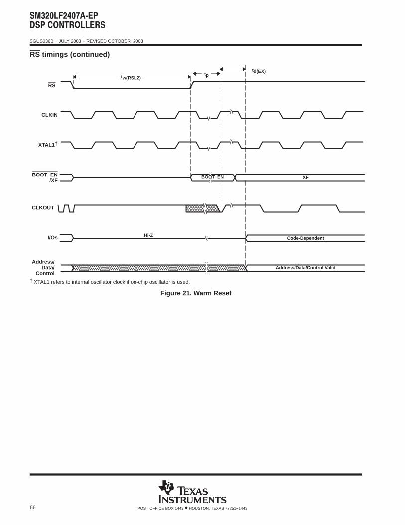
SGUS036B − JULY 2003 − REVISED OCTOBER 2003
66 POST OFFICE BOX 1443 • HOUSTON, TEXAS 77251−1443
RS timings (continued)
XTAL1†
Address/Data/
Control
CLKOUT
RS
tw(RSL2)tp
td(EX)
CLKIN
BOOT_EN/XF
I/Os
XF
Code-Dependent
Address/Data/Control Valid
Hi-Z
BOOT_EN
† XTAL1 refers to internal oscillator clock if on-chip oscillator is used.
Figure 21. Warm Reset
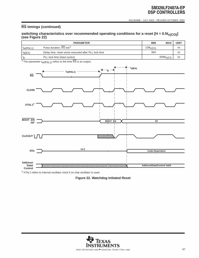
SGUS036B − JULY 2003 − REVISED OCTOBER 2003
67POST OFFICE BOX 1443 • HOUSTON, TEXAS 77251−1443
RS timings (continued)
switching characteristics over recommended operating conditions for a reset [H = 0.5t c(CO)](see Figure 22)
PARAMETER MIN MAX UNIT
tw(RSL1) Pulse duration, RS low† 128tc(CI) ns
td(EX) Delay time, reset vector executed after PLL lock time 36H ns
tp PLL lock time (input cycles) 4096tc(CI) ns
† The parameter tw(RSL1) refers to the time RS is an output.
XTAL1†
Address/Data/
Control
CLKOUT
RS
tw(RSL1)tp
td(EX)
CLKIN
BOOT_EN/XF
BOOT_EN
I/Os
XF
Code-Dependent
Address/Data/Control Valid
Hi-Z
† XTAL1 refers to internal oscillator clock if on-chip oscillator is used.
Figure 22. Watchdog Initiated Reset
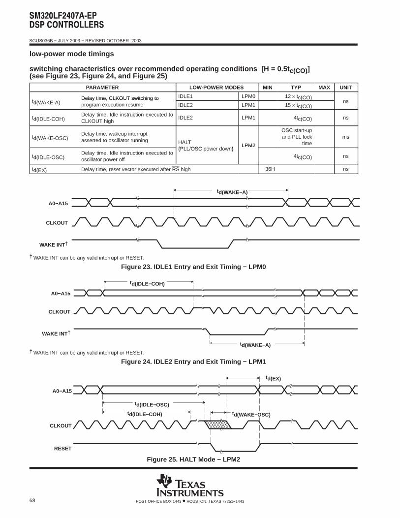
SGUS036B − JULY 2003 − REVISED OCTOBER 2003
68 POST OFFICE BOX 1443 • HOUSTON, TEXAS 77251−1443
low-power mode timings
switching characteristics over recommended operating conditions [H = 0.5t c(CO)](see Figure 23, Figure 24, and Figure 25)
PARAMETER LOW-POWER MODES MIN TYP MAX UNIT
td(WAKE-A)Delay time, CLKOUT switching to IDLE1 LPM0 12 × tc(CO)
nstd(WAKE-A)Delay time, CLKOUT switching toprogram execution resume IDLE2 LPM1 15 × tc(CO)
ns
td(IDLE-COH)Delay time, Idle instruction executed toCLKOUT high
IDLE2 LPM1 4tc(CO) ns
td(WAKE-OSC)Delay time, wakeup interruptasserted to oscillator running HALT
PLL/OSC power downLPM2
OSC start-upand PLL lock
timems
td(IDLE-OSC)Delay time, Idle instruction executed tooscillator power off
PLL/OSC power downLPM2
4tc(CO) ns
td(EX) Delay time, reset vector executed after RS high 36H ns
WAKE INT†
CLKOUT
A0−A15
td(WAKE−A)
† WAKE INT can be any valid interrupt or RESET.
Figure 23. IDLE1 Entry and Exit Timing − LPM0
td(WAKE−A)
td(IDLE−COH)
WAKE INT†
CLKOUT
A0−A15
† WAKE INT can be any valid interrupt or RESET.
Figure 24. IDLE2 Entry and Exit Timing − LPM1
td(EX)
td(IDLE−COH)
td(IDLE−OSC)
ÁÁ
RESET
CLKOUT
A0−A15
td(WAKE−OSC)
Figure 25. HALT Mode − LPM2
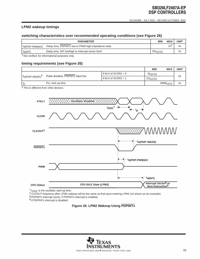
SGUS036B − JULY 2003 − REVISED OCTOBER 2003
69POST OFFICE BOX 1443 • HOUSTON, TEXAS 77251−1443
LPM2 wakeup timings
switching characteristics over recommended operating conditions (see Figure 26)
PARAMETER MIN MAX UNIT
td(PDP-PWM)HZ Delay time, PDPINTx low to PWM high-impedance state 12† ns
td(INT) Delay time, INT low/high to interrupt-vector fetch 10tc(CO) ns
† Not verified; for informational purposes only.
timing requirements (see Figure 26)
MIN MAX UNIT
tw(PDP-WAKE)‡ Pulse duration, PDPINTx input lowif bit 6 of SCSR2 = 0 6tc(CO)
nstw(PDP-WAKE)‡ Pulse duration, PDPINTx input lowif bit 6 of SCSR2 = 1 12tc(CO)
ns
tp PLL lock-up time 4096tc(CI) ns
‡ This is different from 240x devices.
PWM
PDPINTx
CLKOUT‡
tw(PDP−WAKE)
td(PDP-PWM)HZ
CPU StatusInterrupt Vector § orNext Instruction ¶
td(INT)
XTAL1 Oscillator Disabled
CLKIN
tptOSC†
CPU IDLE State (LPM2)
† tOSC is the oscillator start-up time.‡ CLKOUT frequency after LPM2 wakeup will be the same as that upon entering LPM2 (x4 shown as an example).§ PDPINTx interrupt vector, if PDPINTx interrupt is enabled.¶ If PDPINTx interrupt is disabled.
Figure 26. LPM2 Wakeup Using PDPINTx
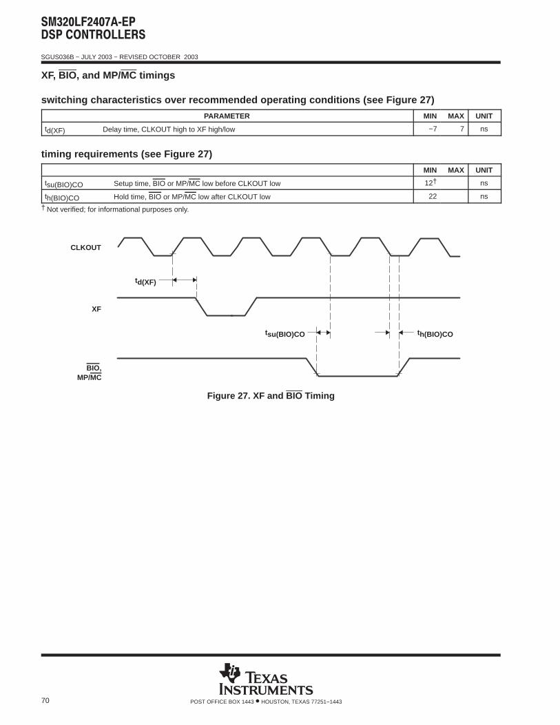
SGUS036B − JULY 2003 − REVISED OCTOBER 2003
70 POST OFFICE BOX 1443 • HOUSTON, TEXAS 77251−1443
XF, BIO, and MP/MC timings
switching characteristics over recommended operating conditions (see Figure 27)
PARAMETER MIN MAX UNIT
td(XF) Delay time, CLKOUT high to XF high/low −7 7 ns
timing requirements (see Figure 27)
MIN MAX UNIT
tsu(BIO)CO Setup time, BIO or MP/MC low before CLKOUT low 12† ns
th(BIO)CO Hold time, BIO or MP/MC low after CLKOUT low 22 ns
† Not verified; for informational purposes only.
td(XF)
XF
BIO,MP/MC
CLKOUT
tsu(BIO)CO th(BIO)CO
Figure 27. XF and BIO Timing
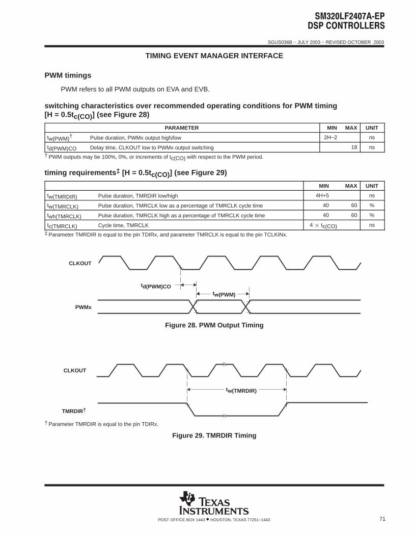
SGUS036B − JULY 2003 − REVISED OCTOBER 2003
71POST OFFICE BOX 1443 • HOUSTON, TEXAS 77251−1443
TIMING EVENT MANAGER INTERFACE
PWM timings
PWM refers to all PWM outputs on EVA and EVB.
switching characteristics over recommended operating conditions for PWM timing[H = 0.5tc(CO)] (see Figure 28)
PARAMETER MIN MAX UNIT
tw(PWM)† Pulse duration, PWMx output high/low 2H−2 ns
td(PWM)CO Delay time, CLKOUT low to PWMx output switching 18 ns
† PWM outputs may be 100%, 0%, or increments of tc(CO) with respect to the PWM period.
timing requirements ‡ [H = 0.5tc(CO)] (see Figure 29)
MIN MAX UNIT
tw(TMRDIR) Pulse duration, TMRDIR low/high 4H+5 ns
tw(TMRCLK) Pulse duration, TMRCLK low as a percentage of TMRCLK cycle time 40 60 %
twh(TMRCLK) Pulse duration, TMRCLK high as a percentage of TMRCLK cycle time 40 60 %
tc(TMRCLK) Cycle time, TMRCLK 4 tc(CO) ns
‡ Parameter TMRDIR is equal to the pin TDIRx, and parameter TMRCLK is equal to the pin TCLKINx.
tw(PWM)
td(PWM)CO
PWMx
CLKOUT
Figure 28. PWM Output Timing
CLKOUT
tw(TMRDIR)
TMRDIR†
† Parameter TMRDIR is equal to the pin TDIRx.
Figure 29. TMRDIR Timing
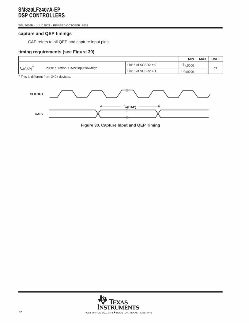
SGUS036B − JULY 2003 − REVISED OCTOBER 2003
72 POST OFFICE BOX 1443 • HOUSTON, TEXAS 77251−1443
capture and QEP timings
CAP refers to all QEP and capture input pins.
timing requirements (see Figure 30)
MIN MAX UNIT
tw(CAP)† Pulse duration, CAPx input low/highif bit 6 of SCSR2 = 0 6tc(CO)
nstw(CAP)† Pulse duration, CAPx input low/highif bit 6 of SCSR2 = 1 12tc(CO)
ns
† This is different from 240x devices.
CAPx
tw(CAP)
CLKOUT
Figure 30. Capture Input and QEP Timing
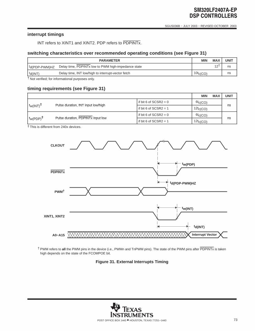
SGUS036B − JULY 2003 − REVISED OCTOBER 2003
73POST OFFICE BOX 1443 • HOUSTON, TEXAS 77251−1443
interrupt timings
INT refers to XINT1 and XINT2. PDP refers to PDPINTx.
switching characteristics over recommended operating conditions (see Figure 31)
PARAMETER MIN MAX UNIT
td(PDP-PWM)HZ Delay time, PDPINTx low to PWM high-impedance state 12† ns
td(INT) Delay time, INT low/high to interrupt-vector fetch 10tc(CO) ns
† Not verified; for informational purposes only.
timing requirements (see Figure 31)
MIN MAX UNIT
tw(INT)‡ Pulse duration, INT input low/highif bit 6 of SCSR2 = 0 6tc(CO)
nstw(INT)‡ Pulse duration, INT input low/highif bit 6 of SCSR2 = 1 12tc(CO)
ns
tw(PDP)‡ Pulse duration, PDPINTx input lowif bit 6 of SCSR2 = 0 6tc(CO)
nstw(PDP)‡ Pulse duration, PDPINTx input lowif bit 6 of SCSR2 = 1 12tc(CO)
ns
‡ This is different from 240x devices.
PWM†
PDPINTx
CLKOUT
tw(PDP)
td(PDP-PWM)HZ
XINT1, XINT2
tw(INT)
Interrupt Vector
td(INT)
† PWM refers to all the PWM pins in the device (i.e., PWMn and TnPWM pins). The state of the PWM pins after PDPINTx is takenhigh depends on the state of the FCOMPOE bit.
A0−A15
Figure 31. External Interrupts Timing
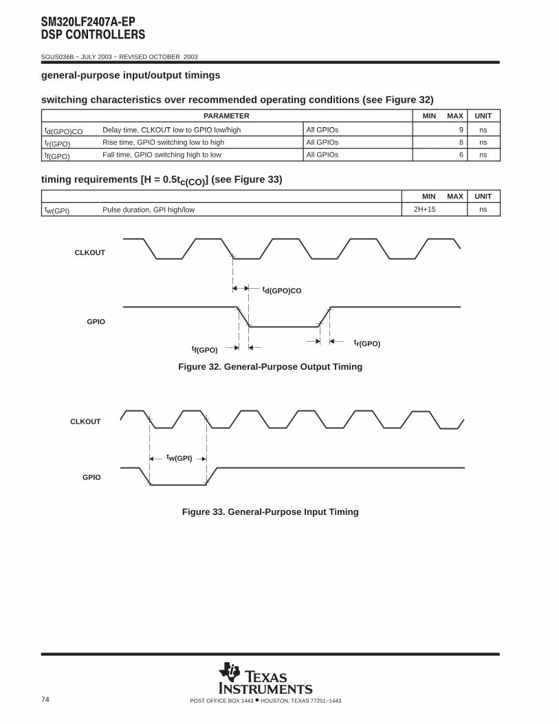
SGUS036B − JULY 2003 − REVISED OCTOBER 2003
74 POST OFFICE BOX 1443 • HOUSTON, TEXAS 77251−1443
general-purpose input/output timings
switching characteristics over recommended operating conditions (see Figure 32)
PARAMETER MIN MAX UNIT
td(GPO)CO Delay time, CLKOUT low to GPIO low/high All GPIOs 9 nstd(GPO)CO Delay time, CLKOUT low to GPIO low/high All GPIOs 9 ns
tr(GPO) Rise time, GPIO switching low to high All GPIOs 8 ns
tf(GPO) Fall time, GPIO switching high to low All GPIOs 6 ns
timing requirements [H = 0.5t c(CO)] (see Figure 33)
MIN MAX UNIT
tw(GPI) Pulse duration, GPI high/low 2H+15 ns
td(GPO)CO
GPIO
CLKOUT
tr(GPO)tf(GPO)
Figure 32. General-Purpose Output Timing
GPIO
CLKOUT
tw(GPI)
Figure 33. General-Purpose Input Timing
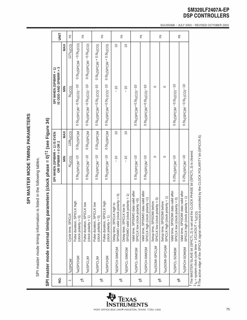
-
SGUS036B − JULY 2003 − REVISED OCTOBER 2003
POST OFFICE BOX 1443 HOUSTON, TEXAS 77251−1443• 75
SP
I MA
ST
ER
MO
DE
TIM
ING
PA
RA
ME
TE
RS
SP
I mas
ter
mod
e tim
ing
info
rmat
ion
is li
sted
in th
e fo
llow
ing
tabl
es.
SP
I mas
ter
mod
e ex
tern
al ti
min
g pa
ram
eter
s (c
lock
pha
se =
0)
†‡ (
see
Fig
ure
34)
NO
.
SP
I WH
EN
(S
PIB
RR
+ 1
) IS
EV
EN
OR
SP
IBR
R =
0 O
R 2
SP
I WH
EN
(S
PIB
RR
+ 1
)IS
OD
D A
ND
SP
IBR
R >
3U
NIT
NO
.M
INM
AX
MIN
MA
XU
NIT
1t c
(SP
C)M
Cyc
le ti
me,
SP
ICLK
4tc(
CO
)12
8tc(
CO
)5t
c(C
O)
127t
c(C
O)
ns
2§t w
(SP
CH
)MP
ulse
dur
atio
n, S
PIC
LK h
igh
(clo
ck p
olar
ity =
0)
0.5t
c(S
PC
)M−
100.
5tc(
SP
C)M
0.5t
c(S
PC
)M−
0.5t
c(C
O)−
100.
5tc(
SP
C)M
−0.
5tc(
CO
)ns
2§
t w(S
PC
L)M
Pul
se d
urat
ion,
SP
ICLK
low
(clo
ck p
olar
ity =
1)
0.5t
c(S
PC
)M−
100.
5tc(
SP
C)M
0.5t
c(S
PC
)M−
0.5t
c(C
O)−
100.
5tc(
SP
C)M
−0.
5tc(
CO
)
ns
3§t w
(SP
CL)
MP
ulse
dur
atio
n, S
PIC
LK lo
w(c
lock
pol
arity
= 0
)0.
5tc(
SP
C)M
−10
0.5t
c(S
PC
)M0.
5tc(
SP
C)M
+0.
5tc
(CO
)−10
0.5t
c(S
PC
)M +
0.5
t c(C
O)
ns3§
t w(S
PC
H)M
Pul
se d
urat
ion,
SP
ICLK
hig
h(c
lock
pol
arity
= 1
)0.
5tc(
SP
C)M
−10
0.5t
c(S
PC
)M0.
5tc(
SP
C)M
+0.
5tc
(CO
)−10
0.5t
c(S
PC
)M +
0.5
t c(C
O)
ns
4§t d
(SP
CH
-SIM
O)M
Del
ay ti
me,
SP
ICLK
hig
h to
SP
ISIM
O v
alid
(cl
ock
pola
rity
= 0
)−
1010
− 10
10
ns4§
t d(S
PC
L-S
IMO
)MD
elay
tim
e, S
PIC
LK lo
w to
SP
ISIM
O v
alid
(cl
ock
pola
rity
= 1
)−
1010
− 10
10ns
5§t v
(SP
CL-
SIM
O)M
Val
id ti
me,
SP
ISIM
O d
ata
valid
afte
rS
PIC
LK lo
w (
cloc
k po
larit
y =
0)0.
5tc(
SP
C)M
−10
0.5t
c(S
PC
)M+
0.5t
c(C
O)−
10
ns5§
t v(S
PC
H-S
IMO
)MV
alid
tim
e, S
PIS
IMO
dat
a va
lid a
fter
SP
ICLK
hig
h (c
lock
pol
arity
=1)
0.5t
c(S
PC
)M−
100.
5tc(
SP
C)M
+0.
5tc(
CO
)−10
ns
8§t s
u(S
OM
I-S
PC
L)M
Set
up ti
me,
SP
ISO
MI b
efor
e S
PIC
LK lo
w (
cloc
k po
larit
y =
0)
00
ns8§
t su(
SO
MI-
SP
CH
)MS
etup
tim
e, S
PIS
OM
I bef
ore
SP
ICLK
hig
h (c
lock
pol
arity
= 1
)0
0ns
9§t v
(SP
CL-
SO
MI)
MV
alid
tim
e, S
PIS
OM
I dat
a va
lid a
fter
SP
ICLK
low
(cl
ock
pola
rity
= 0
)0.
25t c
(SP
C)M
−10
0.5t
c(S
PC
)M−
0.5t
c(C
O)−
10
ns9§
t v(S
PC
H-S
OM
I)M
Val
id ti
me,
SP
ISO
MI d
ata
valid
afte
rS
PIC
LK h
igh
(clo
ck p
olar
ity =
1)
0.25
t c(S
PC
)M−
100.
5tc(
SP
C)M
−0.
5tc
(CO
)−10
ns
†T
he M
AS
TE
R/S
LAV
E b
it (S
PIC
TL.
2) is
set
and
the
CLO
CK
PH
AS
E b
it (S
PIC
TL.
3) is
cle
ared
.‡
t c =
sys
tem
clo
ck c
ycle
tim
e =
1/C
LKO
UT
= t c
(CO
)§
The
act
ive
edge
of t
he S
PIC
LK s
igna
l ref
eren
ced
is c
ontr
olle
d by
the
CLO
CK
PO
LAR
ITY
bit
(SP
ICC
R.6
).
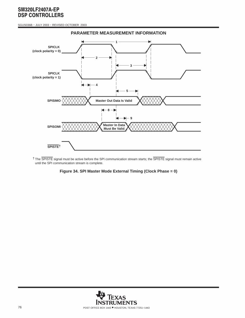
SGUS036B − JULY 2003 − REVISED OCTOBER 2003
76 POST OFFICE BOX 1443 • HOUSTON, TEXAS 77251−1443
PARAMETER MEASUREMENT INFORMATION
9
4
SPISOMI
SPISIMO
SPICLK (clock polarity = 1)
SPICLK (clock polarity = 0)
Master In DataMust Be Valid
Master Out Data Is Valid
8
5
3
2
1
SPISTE†
† The SPISTE signal must be active before the SPI communication stream starts; the SPISTE signal must remain activeuntil the SPI communication stream is complete.
Figure 34. SPI Master Mode External Timing (Clock Phase = 0)
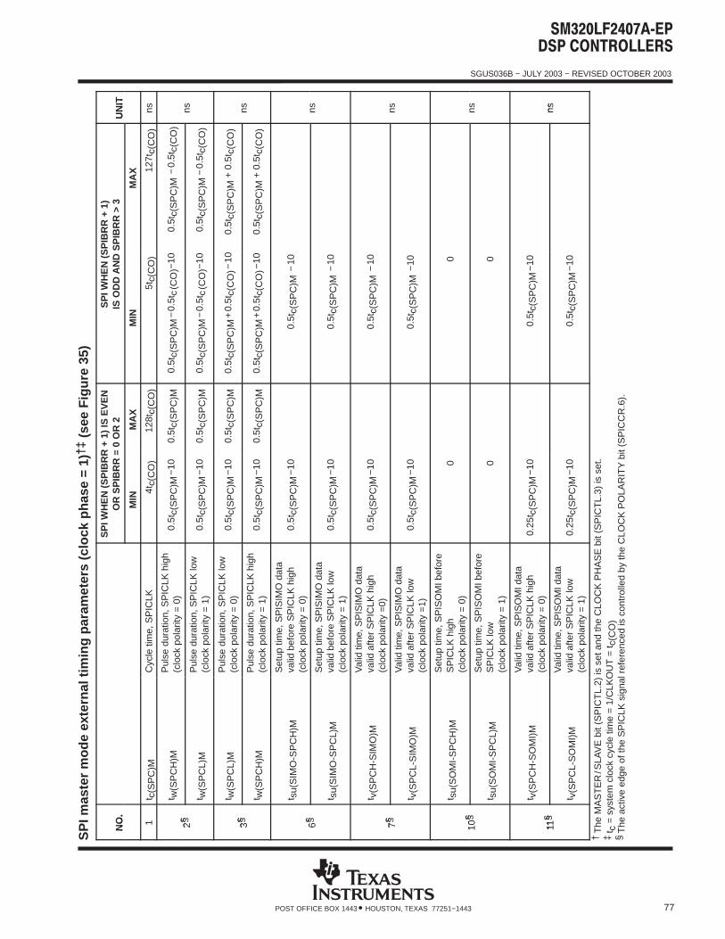
-
SGUS036B − JULY 2003 − REVISED OCTOBER 2003
POST OFFICE BOX 1443 HOUSTON, TEXAS 77251−1443• 77
SP
I mas
ter
mod
e ex
tern
al ti
min
g pa
ram
eter
s (c
lock
pha
se =
1)
†‡ (
see
Fig
ure
35)
NO
.
SP
I WH
EN
(S
PIB
RR
+ 1
) IS
EV
EN
OR
SP
IBR
R =
0 O
R 2
SP
I WH
EN
(S
PIB
RR
+ 1
)IS
OD
D A
ND
SP
IBR
R >
3U
NIT
NO
.M
INM
AX
MIN
MA
XU
NIT
1t c
(SP
C)M
Cyc
le ti
me,
SP
ICLK
4tc(
CO
)12
8tc(
CO
)5t
c(C
O)
127t
c(C
O)
ns
2§t w
(SP
CH
)MP
ulse
dur
atio
n, S
PIC
LK h
igh
(clo
ck p
olar
ity =
0)
0.5t
c(S
PC
)M−
100.
5tc(
SP
C)M
0.5t
c(S
PC
)M−
0.5t
c(C
O)−
100.
5tc(
SP
C)M
−0.
5tc(
CO
)ns
2§
t w(S
PC
L)M
Pul
se d
urat
ion,
SP
ICLK
low
(clo
ck p
olar
ity =
1)
0.5t
c(S
PC
)M−
100.
5tc(
SP
C)M
0.5t
c(S
PC
)M−
0.5t
c(C
O)−
100.
5tc(
SP
C)M
−0.
5tc(
CO
)
ns
3§t w
(SP
CL)
MP
ulse
dur
atio
n, S
PIC
LK lo
w(c
lock
pol
arity
= 0
)0.
5tc(
SP
C)M
−10
0.5t
c(S
PC
)M0.
5tc(
SP
C)M
+0.
5tc(
CO
)−10
0.5t
c(S
PC
)M +
0.5
t c(C
O)
ns3§
t w(S
PC
H)M
Pul
se d
urat
ion,
SP
ICLK
hig
h(c
lock
pol
arity
= 1
)0.
5tc(
SP
C)M
−10
0.5t
c(S
PC
)M0.
5tc(
SP
C)M
+0.
5tc(
CO
)−10
0.5t
c(S
PC
)M +
0.5
t c(C
O)
ns
6§
t su(
SIM
O-S
PC
H)M
Set
up ti
me,
SP
ISIM
O d
ata
valid
bef
ore
SP
ICLK
hig
h(c
lock
pol
arity
= 0
)0.
5tc(
SP
C)M
−10
0.5t
c(S
PC
)M −
10
ns6§
t su(
SIM
O-S
PC
L)M
Set
up ti
me,
SP
ISIM
O d
ata
valid
bef
ore
SP
ICLK
low
(clo
ck p
olar
ity =
1)
0.5t
c(S
PC
)M−
100.
5tc(
SP
C)M
−10
ns
7§
t v(S
PC
H-S
IMO
)M
Val
id ti
me,
SP
ISIM
O d
ata
valid
afte
r S
PIC
LK h
igh
(clo
ck p
olar
ity =
0)0.
5tc(
SP
C)M
−10
0.5t
c(S
PC
)M −
10
ns7§
t v(S
PC
L-S
IMO
)M
Val
id ti
me,
SP
ISIM
O d
ata
valid
afte
r S
PIC
LK lo
w(c
lock
pol
arity
=1)
0.5t
c(S
PC
)M−
100.
5tc(
SP
C)M
−10
ns
10§
t su(
SO
MI-
SP
CH
)M
Set
up ti
me,
SP
ISO
MI b
efor
eS
PIC
LK h
igh
(clo
ck p
olar
ity =
0)
00
ns10
§
t su(
SO
MI-
SP
CL)
M
Set
up ti
me,
SP
ISO
MI b
efor
eS
PIC
LK lo
w(c
lock
pol
arity
= 1
)0
0
ns
11§
t v(S
PC
H-S
OM
I)M
Val
id ti
me,
SP
ISO
MI d
ata
valid
afte
r S
PIC
LK h
igh
(clo
ck p
olar
ity =
0)
0.25
t c(S
PC
)M−
100.
5tc(
SP
C)M
−10
ns11
§
t v(S
PC
L-S
OM
I)M
Val
id ti
me,
SP
ISO
MI d
ata
valid
afte
r S
PIC
LK lo
w(c
lock
pol
arity
= 1
)0.
25t c
(SP
C)M
−10
0.5t
c(S
PC
)M−
10
ns
†T
he M
AS
TE
R/S
LAV
E b
it (S
PIC
TL.
2) is
set
and
the
CLO
CK
PH
AS
E b
it (S
PIC
TL.
3) is
set
.‡
t c =
sys
tem
clo
ck c
ycle
tim
e =
1/C
LKO
UT
= t c
(CO
)§
The
act
ive
edge
of t
he S
PIC
LK s
igna
l ref
eren
ced
is c
ontr
olle
d by
the
CLO
CK
PO
LAR
ITY
bit
(SP
ICC
R.6
).
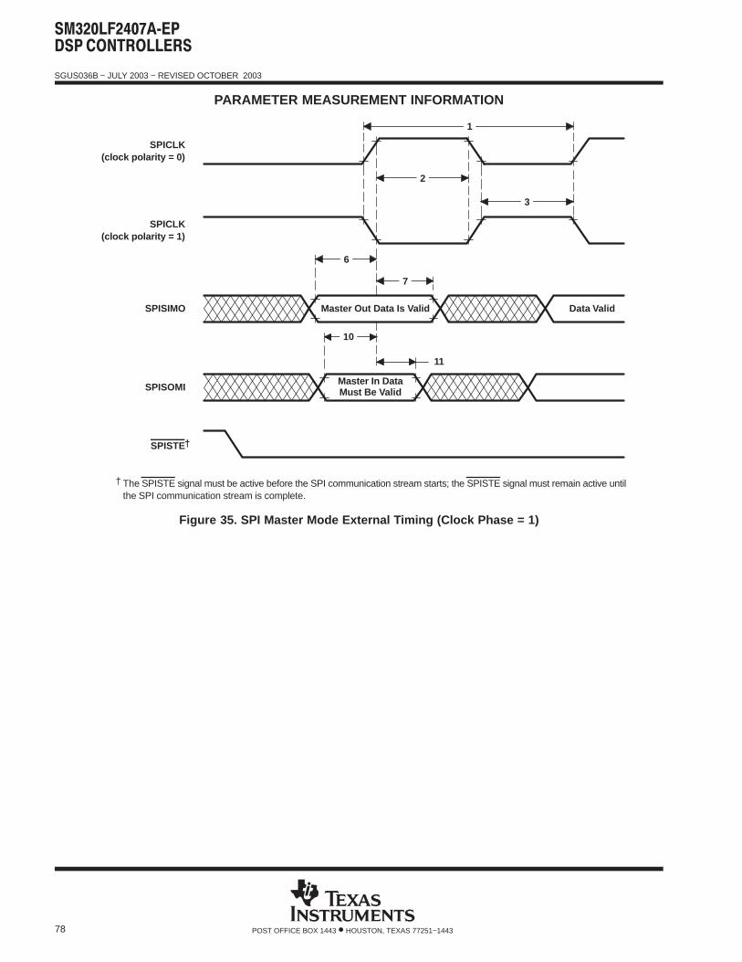
SGUS036B − JULY 2003 − REVISED OCTOBER 2003
78 POST OFFICE BOX 1443 • HOUSTON, TEXAS 77251−1443
PARAMETER MEASUREMENT INFORMATION
Data Valid
11
SPISOMI
SPISIMO
SPICLK (clock polarity = 1)
SPICLK (clock polarity = 0)
Master In DataMust Be V alid
Master Out Data Is Valid
1
7
6
10
3
2
SPISTE†
† The SPISTE signal must be active before the SPI communication stream starts; the SPISTE signal must remain active untilthe SPI communication stream is complete.
Figure 35. SPI Master Mode External Timing (Clock Phase = 1)
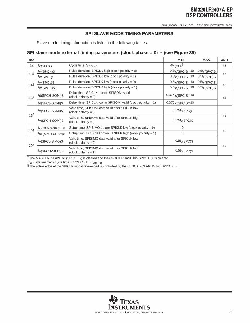
SGUS036B − JULY 2003 − REVISED OCTOBER 2003
79POST OFFICE BOX 1443 • HOUSTON, TEXAS 77251−1443
SPI SLAVE MODE TIMING PARAMETERS
Slave mode timing information is listed in the following tables.
SPI slave mode external timing parameters (clock phase = 0) †‡ (see Figure 36)
NO. MIN MAX UNIT
12 tc(SPC)S Cycle time, SPICLK 4tc(CO)‡ ns
13§tw(SPCH)S Pulse duration, SPICLK high (clock polarity = 0) 0.5tc(SPC)S−10 0.5tc(SPC)S
ns13§tw(SPCL)S Pulse duration, SPICLK low (clock polarity = 1) 0.5tc(SPC)S−10 0.5tc(SPC)S
ns
14§tw(SPCL)S Pulse duration, SPICLK low (clock polarity = 0) 0.5tc(SPC)S−10 0.5tc(SPC)S
ns14§tw(SPCH)S Pulse duration, SPICLK high (clock polarity = 1) 0.5tc(SPC)S−10 0.5tc(SPC)S
ns
15§td(SPCH-SOMI)S
Delay time, SPICLK high to SPISOMI valid(clock polarity = 0)
0.375tc(SPC)S−10ns15§
td(SPCL-SOMI)S Delay time, SPICLK low to SPISOMI valid (clock polarity = 1) 0.375tc(SPC)S−10ns
16§tv(SPCL-SOMI)S
Valid time, SPISOMI data valid after SPICLK low(clock polarity =0)
0.75tc(SPC)Sns16§
tv(SPCH-SOMI)SValid time, SPISOMI data valid after SPICLK high(clock polarity =1)
0.75tc(SPC)S
ns
19§tsu(SIMO-SPCL)S Setup time, SPISIMO before SPICLK low (clock polarity = 0) 0
ns19§tsu(SIMO-SPCH)S Setup time, SPISIMO before SPICLK high (clock polarity = 1) 0
ns
20§tv(SPCL-SIMO)S
Valid time, SPISIMO data valid after SPICLK low(clock polarity = 0)
0.5tc(SPC)Sns20§
tv(SPCH-SIMO)SValid time, SPISIMO data valid after SPICLK high(clock polarity = 1)
0.5tc(SPC)S
ns
† The MASTER/SLAVE bit (SPICTL.2) is cleared and the CLOCK PHASE bit (SPICTL.3) is cleared.‡ tc = system clock cycle time = 1/CLKOUT = tc(CO)§ The active edge of the SPICLK signal referenced is controlled by the CLOCK POLARITY bit (SPICCR.6).

SGUS036B − JULY 2003 − REVISED OCTOBER 2003
80 POST OFFICE BOX 1443 • HOUSTON, TEXAS 77251−1443
PARAMETER MEASUREMENT INFORMATION
20
15
SPISIMO
SPISOMI
SPICLK(clock polarity = 1)
SPICLK(clock polarity = 0)
SPISIMO DataMust Be V alid
SPISOMI Data Is Valid
19
16
14
13
12
SPISTE†
† The SPISTE signal must be active before the SPI communication stream starts; the SPISTE signal must remain active untilthe SPI communication stream is complete.
Figure 36. SPI Slave Mode External Timing (Clock Phase = 0)
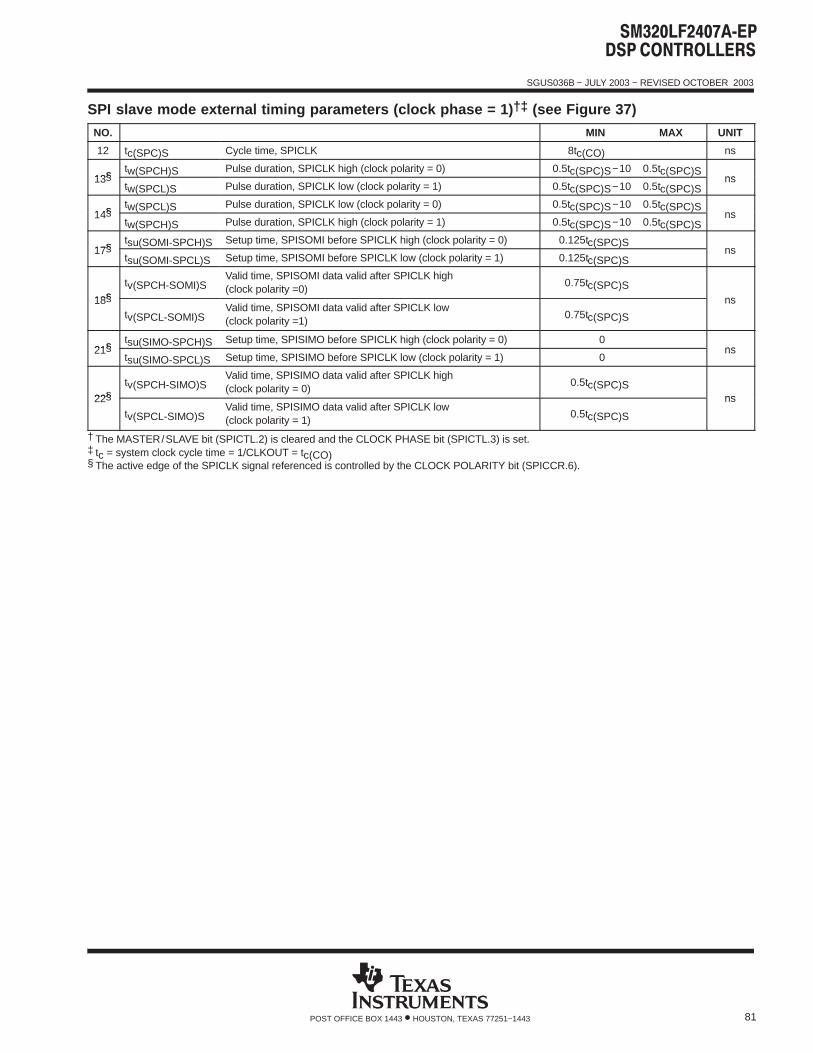
SGUS036B − JULY 2003 − REVISED OCTOBER 2003
81POST OFFICE BOX 1443 • HOUSTON, TEXAS 77251−1443
SPI slave mode external timing parameters (clock phase = 1) †‡ (see Figure 37)
NO. MIN MAX UNIT
12 tc(SPC)S Cycle time, SPICLK 8tc(CO) ns
13§tw(SPCH)S Pulse duration, SPICLK high (clock polarity = 0) 0.5tc(SPC)S−10 0.5tc(SPC)S
ns13§tw(SPCL)S Pulse duration, SPICLK low (clock polarity = 1) 0.5tc(SPC)S−10 0.5tc(SPC)S
ns
14§tw(SPCL)S Pulse duration, SPICLK low (clock polarity = 0) 0.5tc(SPC)S−10 0.5tc(SPC)S
ns14§tw(SPCH)S Pulse duration, SPICLK high (clock polarity = 1) 0.5tc(SPC)S−10 0.5tc(SPC)S
ns
17§tsu(SOMI-SPCH)S Setup time, SPISOMI before SPICLK high (clock polarity = 0) 0.125tc(SPC)S
ns17§tsu(SOMI-SPCL)S Setup time, SPISOMI before SPICLK low (clock polarity = 1) 0.125tc(SPC)S
ns
18§tv(SPCH-SOMI)S
Valid time, SPISOMI data valid after SPICLK high(clock polarity =0)
0.75tc(SPC)Sns18§
tv(SPCL-SOMI)SValid time, SPISOMI data valid after SPICLK low(clock polarity =1)
0.75tc(SPC)S
ns
21§tsu(SIMO-SPCH)S Setup time, SPISIMO before SPICLK high (clock polarity = 0) 0
ns21§tsu(SIMO-SPCL)S Setup time, SPISIMO before SPICLK low (clock polarity = 1) 0
ns
22§tv(SPCH-SIMO)S
Valid time, SPISIMO data valid after SPICLK high(clock polarity = 0)
0.5tc(SPC)Sns22§
tv(SPCL-SIMO)SValid time, SPISIMO data valid after SPICLK low(clock polarity = 1)
0.5tc(SPC)S
ns
† The MASTER/SLAVE bit (SPICTL.2) is cleared and the CLOCK PHASE bit (SPICTL.3) is set.‡ tc = system clock cycle time = 1/CLKOUT = tc(CO)§ The active edge of the SPICLK signal referenced is controlled by the CLOCK POLARITY bit (SPICCR.6).

SGUS036B − JULY 2003 − REVISED OCTOBER 2003
82 POST OFFICE BOX 1443 • HOUSTON, TEXAS 77251−1443
PARAMETER MEASUREMENT INFORMATION
Data Valid
22
SPISIMO
SPISOMI
SPICLK(clock polarity = 1)
SPICLK(clock polarity = 0)
SPISIMO DataMust Be V alid
SPISOMI Data Is Valid
21
12
18
17
14
13
SPISTE†
† The SPISTE signal must be active before the SPI communication stream starts; the SPISTE signal must remain active untilthe SPI communication stream is complete.
Figure 37. SPI Slave Mode External Timing (Clock Phase = 1)
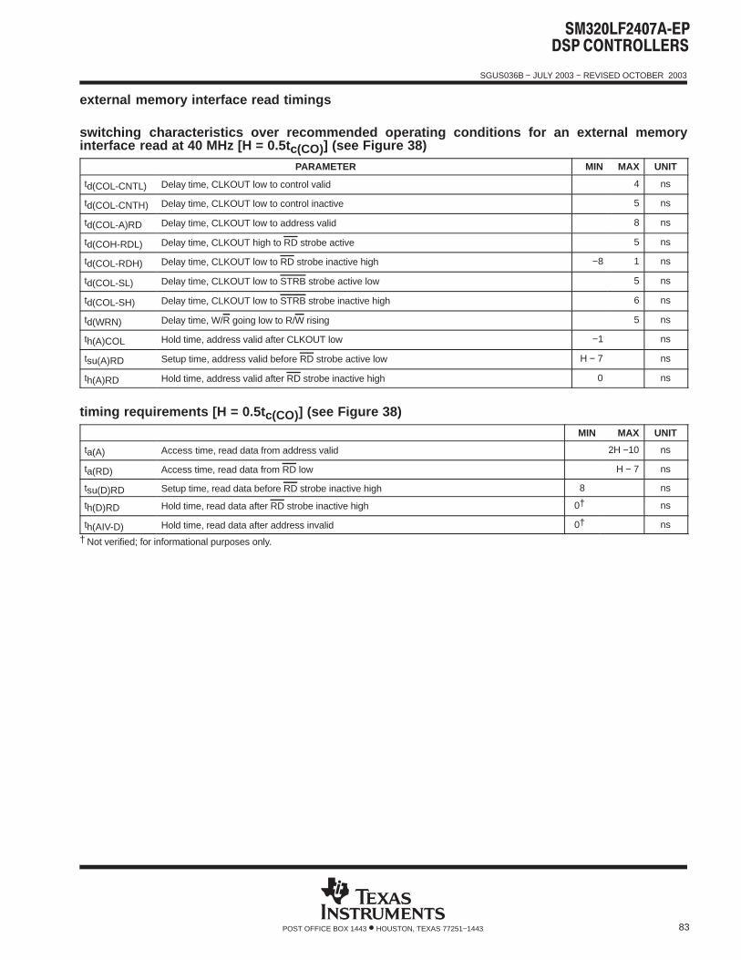
SGUS036B − JULY 2003 − REVISED OCTOBER 2003
83POST OFFICE BOX 1443 • HOUSTON, TEXAS 77251−1443
external memory interface read timings
switching characteristics over recommended operating conditions for an external memoryinterface read at 40 MHz [H = 0.5t c(CO)] (see Figure 38)
PARAMETER MIN MAX UNIT
td(COL-CNTL) Delay time, CLKOUT low to control valid 4 ns
td(COL-CNTH) Delay time, CLKOUT low to control inactive 5 ns
td(COL-A)RD Delay time, CLKOUT low to address valid 8 ns
td(COH-RDL) Delay time, CLKOUT high to RD strobe active 5 ns
td(COL-RDH) Delay time, CLKOUT low to RD strobe inactive high −8 1 ns
td(COL-SL) Delay time, CLKOUT low to STRB strobe active low 5 ns
td(COL-SH) Delay time, CLKOUT low to STRB strobe inactive high 6 ns
td(WRN) Delay time, W/R going low to R/W rising 5 ns
th(A)COL Hold time, address valid after CLKOUT low −1 ns
tsu(A)RD Setup time, address valid before RD strobe active low H − 7 ns
th(A)RD Hold time, address valid after RD strobe inactive high 0 ns
timing requirements [H = 0.5t c(CO)] (see Figure 38)
MIN MAX UNIT
ta(A) Access time, read data from address valid 2H −10 ns
ta(RD) Access time, read data from RD low H − 7 ns
tsu(D)RD Setup time, read data before RD strobe inactive high 8 ns
th(D)RD Hold time, read data after RD strobe inactive high 0† ns
th(AIV-D) Hold time, read data after address invalid 0† ns
† Not verified; for informational purposes only.
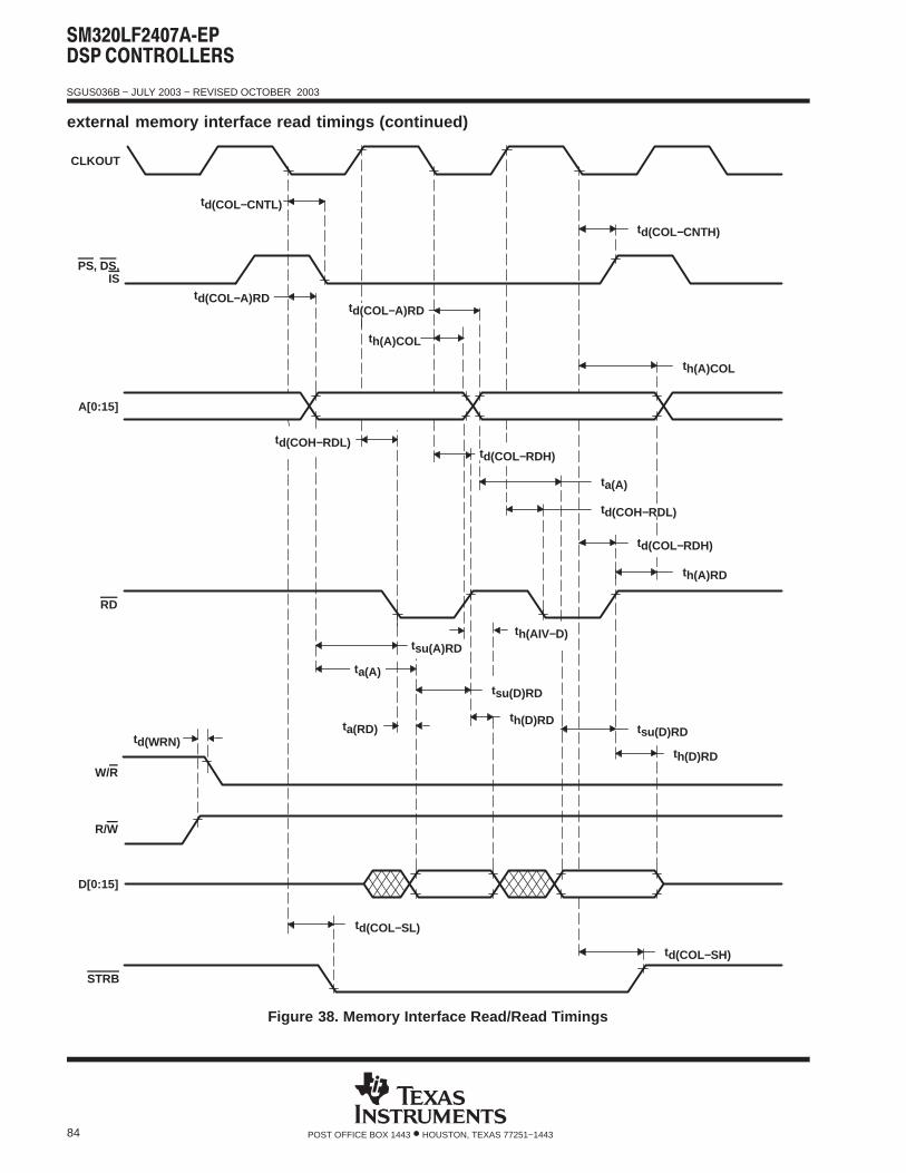
SGUS036B − JULY 2003 − REVISED OCTOBER 2003
84 POST OFFICE BOX 1443 • HOUSTON, TEXAS 77251−1443
external memory interface read timings (continued)
td(COL−CNTH)
th(A)COL
td(COL−A)RD
th(A)COL
td(COL−RDH)td(COH−RDL)
ta(A)
td(COH−RDL)
CLKOUT
PS, DS, IS
A[0:15]
td(COL−CNTL)
td(COL−A)RD
th(A)RD
tsu(D)RD
th(D)RD
tsu(A)RD
th(D)RD
tsu(D)RD
td(COL−SH)
RD
D[0:15]
STRB
td(COL−SL)
td(COL−RDH)
ta(A)
th(AIV−D)
W/R
R/W
ta(RD)td(WRN)
Figure 38. Memory Interface Read/Read Timings
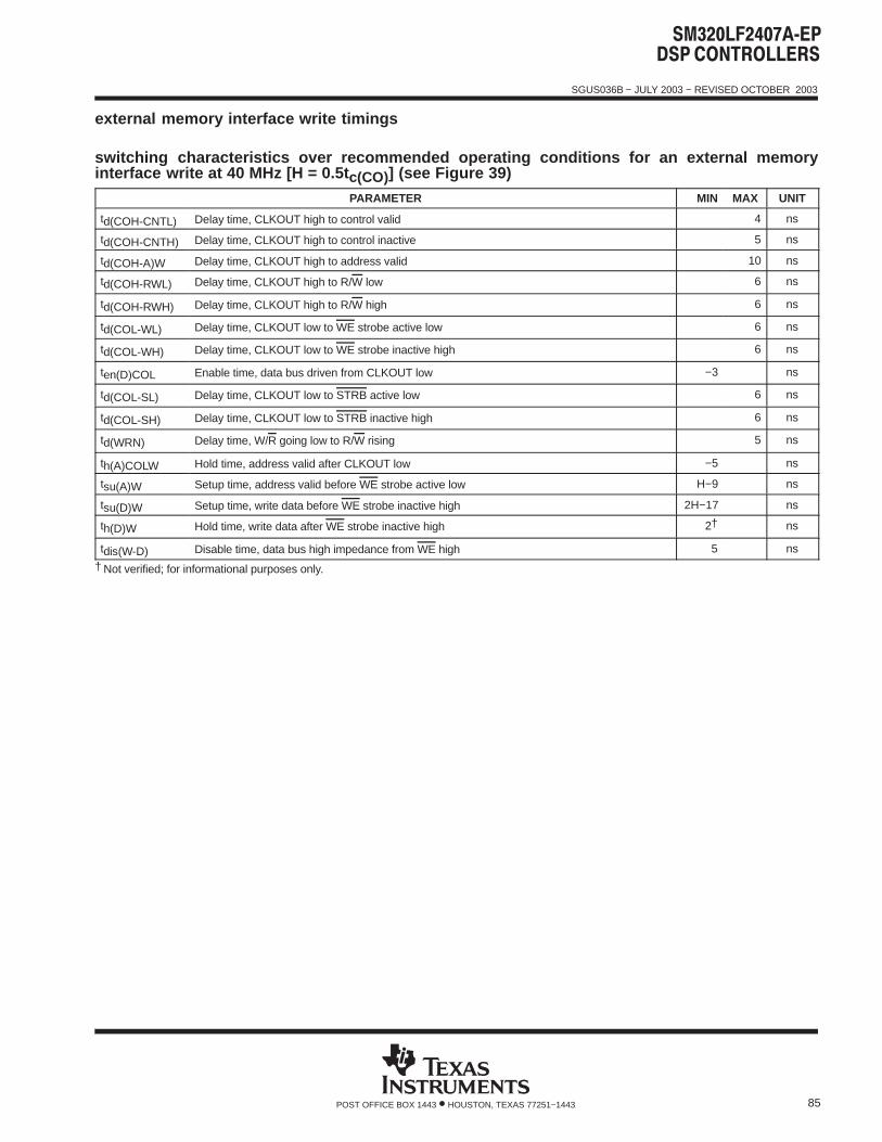
SGUS036B − JULY 2003 − REVISED OCTOBER 2003
85POST OFFICE BOX 1443 • HOUSTON, TEXAS 77251−1443
external memory interface write timings
switching characteristics over recommended operating conditions for an external memoryinterface write at 40 MHz [H = 0.5t c(CO)] (see Figure 39)
PARAMETER MIN MAX UNIT
td(COH-CNTL) Delay time, CLKOUT high to control valid 4 ns
td(COH-CNTH) Delay time, CLKOUT high to control inactive 5 ns
td(COH-A)W Delay time, CLKOUT high to address valid 10 ns
td(COH-RWL) Delay time, CLKOUT high to R/W low 6 ns
td(COH-RWH) Delay time, CLKOUT high to R/W high 6 ns
td(COL-WL) Delay time, CLKOUT low to WE strobe active low 6 ns
td(COL-WH) Delay time, CLKOUT low to WE strobe inactive high 6 ns
ten(D)COL Enable time, data bus driven from CLKOUT low −3 ns
td(COL-SL) Delay time, CLKOUT low to STRB active low 6 ns
td(COL-SH) Delay time, CLKOUT low to STRB inactive high 6 ns
td(WRN) Delay time, W/R going low to R/W rising 5 ns
th(A)COLW Hold time, address valid after CLKOUT low −5 ns
tsu(A)W Setup time, address valid before WE strobe active low H−9 ns
tsu(D)W Setup time, write data before WE strobe inactive high 2H−17 ns
th(D)W Hold time, write data after WE strobe inactive high 2† ns
tdis(W-D) Disable time, data bus high impedance from WE high 5 ns
† Not verified; for informational purposes only.
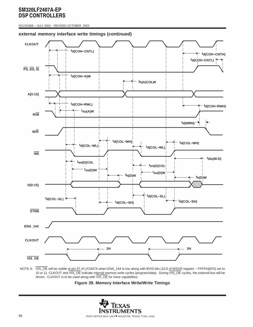
SGUS036B − JULY 2003 − REVISED OCTOBER 2003
86 POST OFFICE BOX 1443 • HOUSTON, TEXAS 77251−1443
external memory interface write timings (continued)
tdis(W-D)
td(COH−A)W
td(COH−RWL)
tsu(A)W
td(COL−WH)
WE
STRB
ten(D)COL
td(COL−WL)
th(A)COLW
td(COH−CNTL)
td(COH−CNTH)
CLKOUT
A[0:15]
R/W
PS, DS, IS
td(COH−CNTL)
td(COH−RWH)
td(COL−WL)
td(COL−WH)
th(D)W
tsu(D)W
ten(D)COL
td(COL−SH)
CLKOUT
ENA_144
VIS_OE
th(D)W
td(COL−SL)
NOTE A: VIS_OE will be visible at pin 97 of LF2407A when ENA_144 is low along with BVIS bits (10,9 of WSGR register − FFFFh@I/O) set to10 or 11. CLKOUT and VIS_OE indicate internal memory write cycles (program/data). During VIS_OE cycles, the external bus will bedriven. CLKOUT is to be used along with VIS_OE for trace capabilities.
tsu(D)W
td(COL−SL)
D[0:15]
td(COL−SH)
2H 2H
W/R
td(WRN)
Figure 39. Memory Interface Write/Write Timings
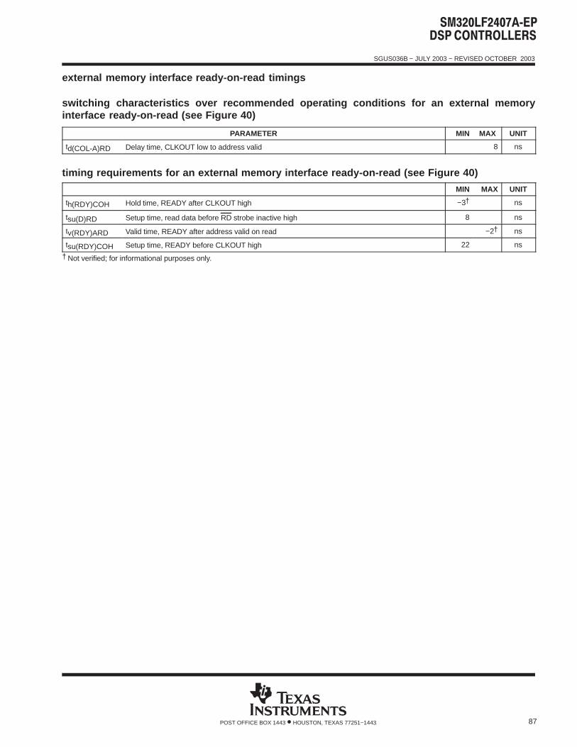
SGUS036B − JULY 2003 − REVISED OCTOBER 2003
87POST OFFICE BOX 1443 • HOUSTON, TEXAS 77251−1443
external memory interface ready-on-read timings
switching characteristics over recommended operating conditions for an external memoryinterface ready-on-read (see Figure 40)
PARAMETER MIN MAX UNIT
td(COL-A)RD Delay time, CLKOUT low to address valid 8 ns
timing requirements for an external memory interface ready-on-read (see Figure 40)
MIN MAX UNIT
th(RDY)COH Hold time, READY after CLKOUT high −3† ns
tsu(D)RD Setup time, read data before RD strobe inactive high 8 ns
tv(RDY)ARD Valid time, READY after address valid on read −2† ns
tsu(RDY)COH Setup time, READY before CLKOUT high 22 ns
† Not verified; for informational purposes only.
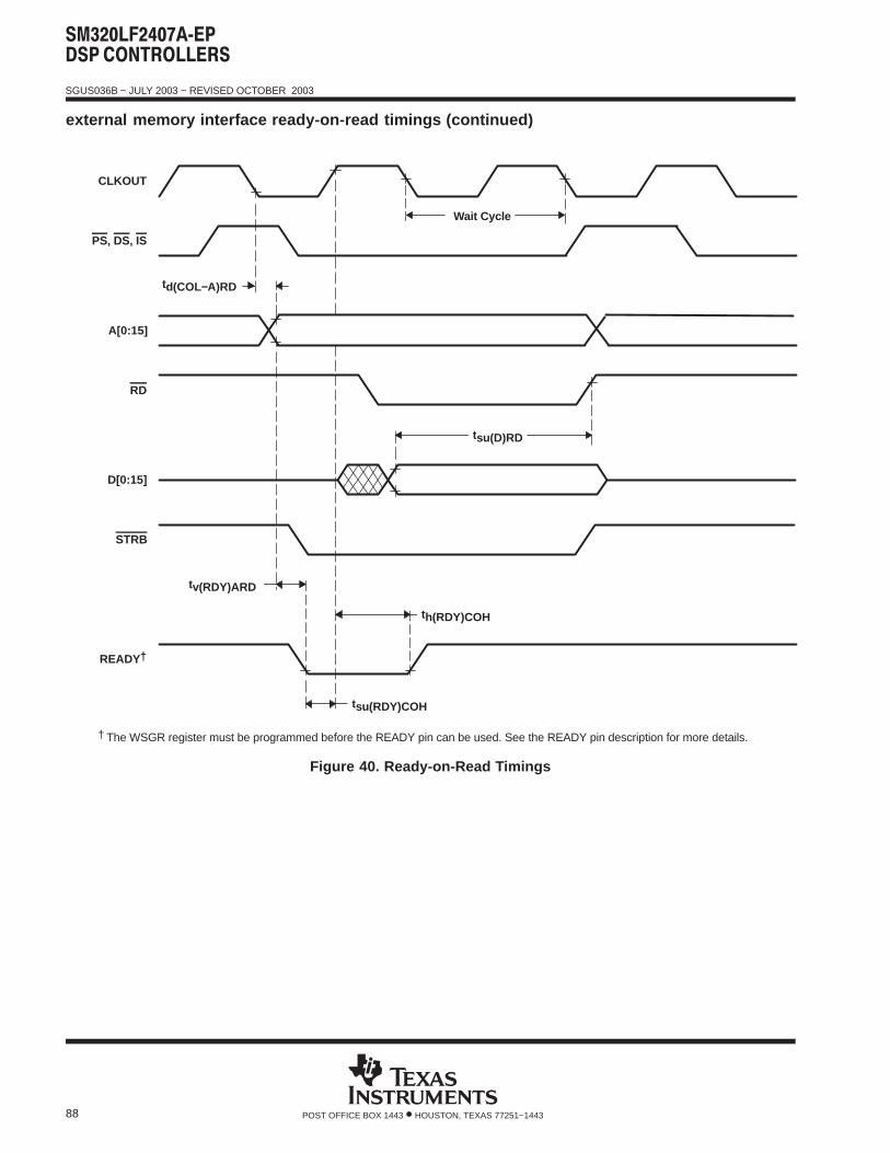
SGUS036B − JULY 2003 − REVISED OCTOBER 2003
88 POST OFFICE BOX 1443 • HOUSTON, TEXAS 77251−1443
external memory interface ready-on-read timings (continued)
th(RDY)COH
CLKOUT
PS, DS, IS
RD
D[0:15]
STRB
A[0:15]
td(COL−A)RD
tv(RDY)ARD
tsu(RDY)COH
READY†
Wait Cycle
tsu(D)RD
† The WSGR register must be programmed before the READY pin can be used. See the READY pin description for more details.
Figure 40. Ready-on-Read Timings
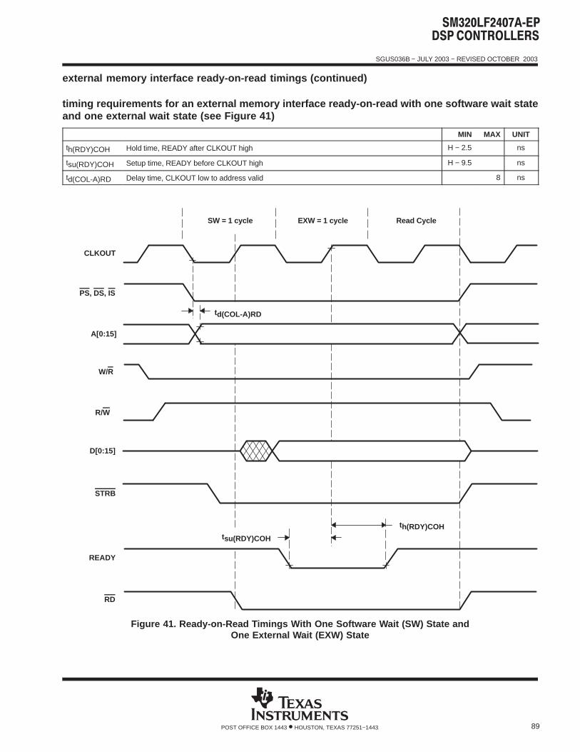
SGUS036B − JULY 2003 − REVISED OCTOBER 2003
89POST OFFICE BOX 1443 • HOUSTON, TEXAS 77251−1443
external memory interface ready-on-read timings (continued)
timing requirements for an external memory interface ready-on-read with one software wait stateand one external wait state (see Figure 41)
MIN MAX UNIT
th(RDY)COH Hold time, READY after CLKOUT high H − 2.5 ns
tsu(RDY)COH Setup time, READY before CLKOUT high H − 9.5 ns
td(COL-A)RD Delay time, CLKOUT low to address valid 8 ns
PS, DS, IS
RD
READY
SW = 1 cycle EXW = 1 cycle Read Cycle
th(RDY)COHtsu(RDY)COH
CLKOUT
R/W
W/R
D[0:15]
STRB
A[0:15]
td(COL-A)RD
Figure 41. Ready-on-Read Timings With One Software Wait (SW) State andOne External Wait (EXW) State
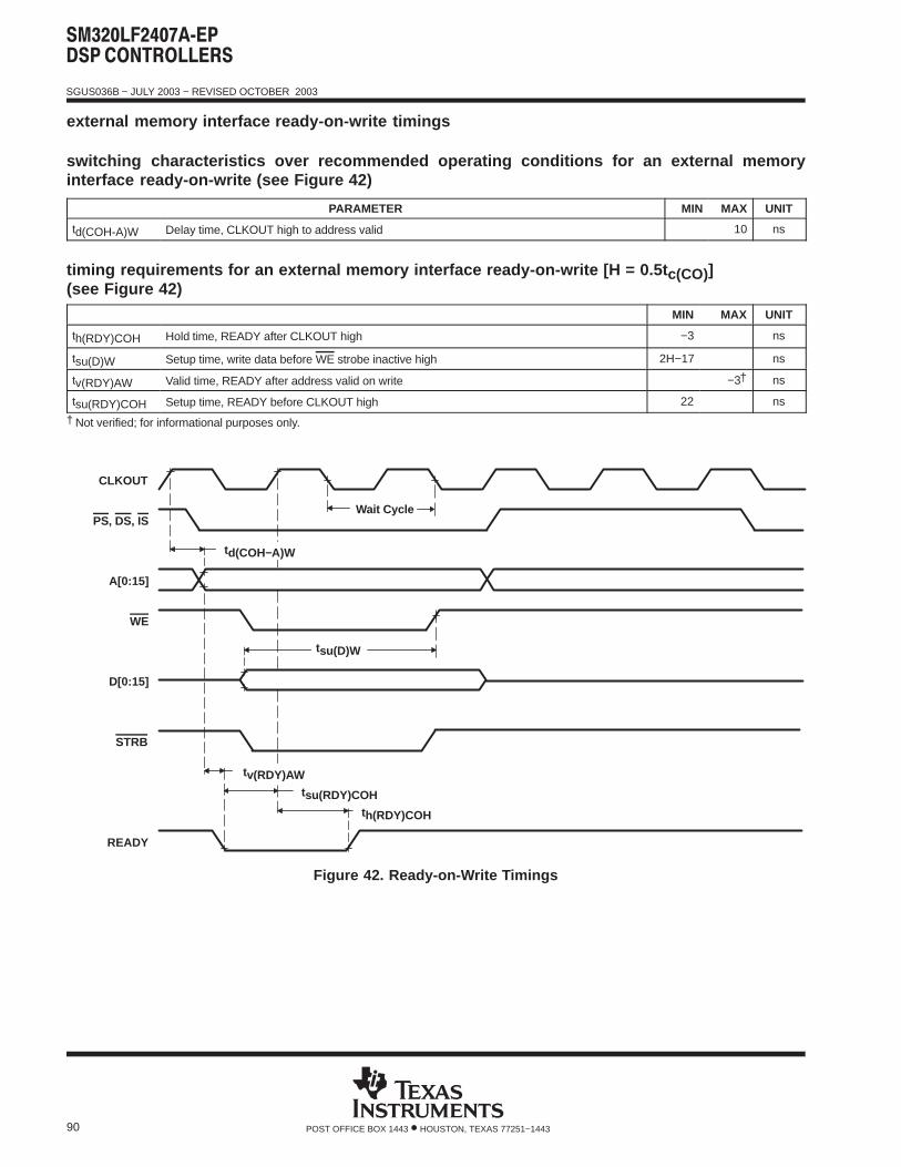
SGUS036B − JULY 2003 − REVISED OCTOBER 2003
90 POST OFFICE BOX 1443 • HOUSTON, TEXAS 77251−1443
external memory interface ready-on-write timings
switching characteristics over recommended operating conditions for an external memoryinterface ready-on-write (see Figure 42)
PARAMETER MIN MAX UNIT
td(COH-A)W Delay time, CLKOUT high to address valid 10 ns
timing requirements for an external memory interface ready-on-write [H = 0.5t c(CO)](see Figure 42)
MIN MAX UNIT
th(RDY)COH Hold time, READY after CLKOUT high −3 ns
tsu(D)W Setup time, write data before WE strobe inactive high 2H−17 ns
tv(RDY)AW Valid time, READY after address valid on write −3† ns
tsu(RDY)COH Setup time, READY before CLKOUT high 22 ns
† Not verified; for informational purposes only.
tsu(D)W
CLKOUT
PS, DS, IS
td(COH−A)W
A[0:15]
WE
D[0:15]
STRB
tsu(RDY)COHth(RDY)COH
READY
tv(RDY)AW
Wait Cycle
Figure 42. Ready-on-Write Timings
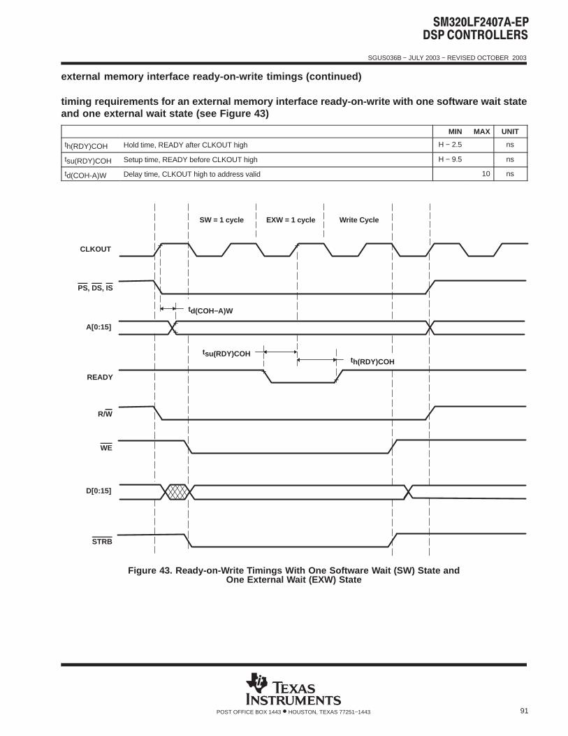
SGUS036B − JULY 2003 − REVISED OCTOBER 2003
91POST OFFICE BOX 1443 • HOUSTON, TEXAS 77251−1443
external memory interface ready-on-write timings (continued)
timing requirements for an external memory interface ready-on-write with one software wait stateand one external wait state (see Figure 43)
MIN MAX UNIT
th(RDY)COH Hold time, READY after CLKOUT high H − 2.5 ns
tsu(RDY)COH Setup time, READY before CLKOUT high H − 9.5 ns
td(COH-A)W Delay time, CLKOUT high to address valid 10 ns
PS, DS, IS
READY
WE
SW = 1 cycle EXW = 1 cycle Write Cycle
D[0:15]
STRB
th(RDY)COHtsu(RDY)COH
CLKOUT
R/W
td(COH−A)W
A[0:15]
Figure 43. Ready-on-Write Timings With One Software Wait (SW) State andOne External Wait (EXW) State
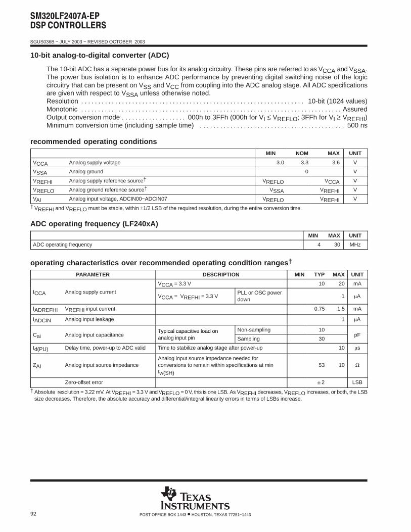
SGUS036B − JULY 2003 − REVISED OCTOBER 2003
92 POST OFFICE BOX 1443 • HOUSTON, TEXAS 77251−1443
10-bit analog-to-digital converter (ADC)
The 10-bit ADC has a separate power bus for its analog circuitry. These pins are referred to as VCCA and VSSA.The power bus isolation is to enhance ADC performance by preventing digital switching noise of the logiccircuitry that can be present on VSS and VCC from coupling into the ADC analog stage. All ADC specificationsare given with respect to VSSA unless otherwise noted.Resolution 10-bit (1024 values). . . . . . . . . . . . . . . . . . . . . . . . . . . . . . . . . . . . . . . . . . . . . . . . . . . . . . . . . . . . . . . . . . Monotonic Assured. . . . . . . . . . . . . . . . . . . . . . . . . . . . . . . . . . . . . . . . . . . . . . . . . . . . . . . . . . . . . . . . . . . . . . . . . . . . . Output conversion mode 000h to 3FFh (000h for VI ≤ VREFLO; 3FFh for VI ≥ VREFHI). . . . . . . . . . . . . . . . . . . Minimum conversion time (including sample time) 500 ns. . . . . . . . . . . . . . . . . . . . . . . . . . . . . . . . . . . . . . . . . . .
recommended operating conditions
MIN NOM MAX UNIT
VCCA Analog supply voltage 3.0 3.3 3.6 V
VSSA Analog ground 0 V
VREFHI Analog supply reference source† VREFLO VCCA V
VREFLO Analog ground reference source† VSSA VREFHI V
VAI Analog input voltage, ADCIN00−ADCIN07 VREFLO VREFHI V
† VREFHI and VREFLO must be stable, within ±1/2 LSB of the required resolution, during the entire conversion time.
ADC operating frequency (LF240xA)
MIN MAX UNIT
ADC operating frequency 4 30 MHz
operating characteristics over recommended operating condition ranges †
PARAMETER DESCRIPTION MIN TYP MAX UNIT
VCCA = 3.3 V 10 20 mA
ICCA Analog supply currentVCCA = VREFHI = 3.3 V
PLL or OSC powerdown
1 A
IADREFHI VREFHI input current 0.75 1.5 mA
IADCIN Analog input leakage 1 A
Cai Analog input capacitanceTypical capacitive load on Non-sampling 10
pFCai Analog input capacitanceTypical capacitive load onanalog input pin Sampling 30
pF
td(PU) Delay time, power-up to ADC valid Time to stabilize analog stage after power-up 10 s
ZAI Analog input source impedanceAnalog input source impedance needed forconversions to remain within specifications at mintw(SH)
53 10 Ω
Zero-offset error 2 LSB
† Absolute resolution = 3.22 mV. At VREFHI = 3.3 V and VREFLO = 0 V, this is one LSB. As VREFHI decreases, VREFLO increases, or both, the LSBsize decreases. Therefore, the absolute accuracy and differential/integral linearity errors in terms of LSBs increase.
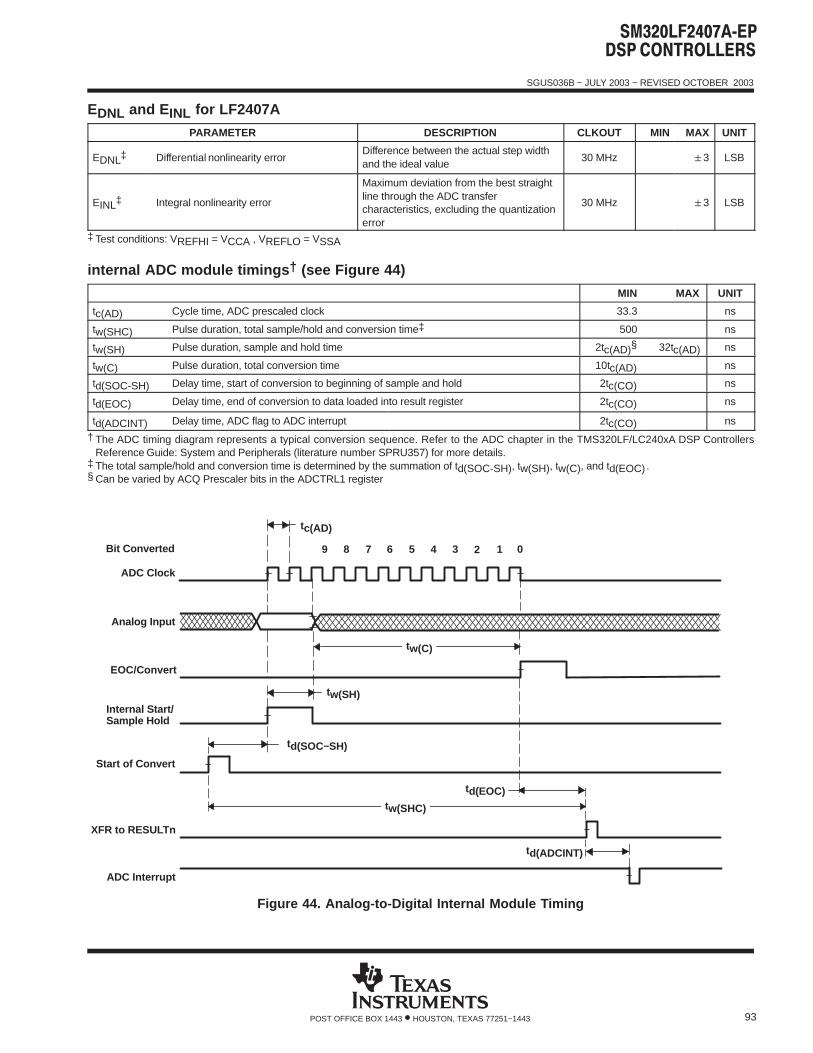
SGUS036B − JULY 2003 − REVISED OCTOBER 2003
93POST OFFICE BOX 1443 • HOUSTON, TEXAS 77251−1443
EDNL and EINL for LF2407A
PARAMETER DESCRIPTION CLKOUT MIN MAX UNIT
EDNL‡ Differential nonlinearity errorDifference between the actual step widthand the ideal value
30 MHz 3 LSB
EINL‡ Integral nonlinearity error
Maximum deviation from the best straightline through the ADC transfercharacteristics, excluding the quantizationerror
30 MHz 3 LSB
‡ Test conditions: VREFHI = VCCA , VREFLO = VSSA
internal ADC module timings † (see Figure 44)
MIN MAX UNIT
tc(AD) Cycle time, ADC prescaled clock 33.3 ns
tw(SHC) Pulse duration, total sample/hold and conversion time‡ 500 ns
tw(SH) Pulse duration, sample and hold time 2tc(AD)§ 32tc(AD) ns
tw(C) Pulse duration, total conversion time 10tc(AD) ns
td(SOC-SH) Delay time, start of conversion to beginning of sample and hold 2tc(CO) ns
td(EOC) Delay time, end of conversion to data loaded into result register 2tc(CO) ns
td(ADCINT) Delay time, ADC flag to ADC interrupt 2tc(CO) ns
† The ADC timing diagram represents a typical conversion sequence. Refer to the ADC chapter in the TMS320LF/LC240xA DSP ControllersReference Guide: System and Peripherals (literature number SPRU357) for more details.
‡ The total sample/hold and conversion time is determined by the summation of td(SOC-SH), tw(SH), tw(C), and td(EOC).§ Can be varied by ACQ Prescaler bits in the ADCTRL1 register
03 245 1
tw(C)
678
tc(AD)
ADC Clock
Analog Input
Bit Converted
td(SOC−SH)
EOC/Convert
Internal Start/Sample Hold
Start of Convert
XFR to RESULTn
tw(SHC)
ÁÁÁÁÁÁ ÁÁÁÁÁÁÁÁÁÁÁÁÁÁÁÁÁÁÁÁÁÁ
td(EOC)
9
tw(SH)
td(ADCINT)
ADC Interrupt
Figure 44. Analog-to-Digital Internal Module Timing
SGUS036B − JULY 2003 − REVISED OCTOBER 2003
94 POST OFFICE BOX 1443 • HOUSTON, TEXAS 77251−1443
Flash parameters @40 MHz CLOCKOUT †
PARAMETER MIN TYP MAX UNIT
‡
Time/Word (16-bit) 30 µs
Clear/Programming time‡ Time/4K Sector 130 msClear/Programming time‡
Time/12K Sector 400 ms
Erase time‡Time/4K Sector 350 ms
Erase time‡Time/12K Sector 1 s
ICCP (VCCP pin current)Indicates the typical/maximum current consumption during theClear-Erase-Program (C-E-P) cycle
5 15 mA
† TI releases upgrades to the Flash algorithms for these devices; hence, these typical values are subject to change.‡ The indicated time does not include the time it takes to load the C-E-P algorithm and the code (to be programmed) onto on-chip RAM. The values
specified are when VDD = 3.3 V and VCCP = 5 V, and any deviation from these values could affect the timing parameters. Aging and process variancecould also impact the timing parameters.
SGUS036B − JULY 2003 − REVISED OCTOBER 2003
95POST OFFICE BOX 1443 • HOUSTON, TEXAS 77251−1443
migrating from 240x devices to 240xA devices
This section highlights the new features/migration issues of the 240xA devices (as compared to the 240x family)and describes the impact these features/issues have on user applications.
maximum clock speed
240xA devices can operate at a maximum speed of 40 MHz compared to the 30-MHz operation of 240x devices.This change in clock speed warrants a change in the register contents of all the peripherals. For example, tomaintain the same baud rate, the divisor values that are loaded to the SPI, SCI, and CAN registers must berecalculated.
code security module
240xA devices incorporate a “code security module” which protects the contents of program memory fromunauthorized duplication. Passwords stored in password locations (PWL) 0040h to 0043h are used for thispurpose. Even if the code is not secured with passwords (i.e., PWL contains FFFFFFFFFFFFFFFFh), the PWLmust still be read to gain access to the program memory contents. Note that locations 0040h to 0043h wereavailable for user code in the 240x devices, which lack the “code security module”. In 240xA devices, theselocations are reserved for the passwords and are not available for the user code. Even if code security featureis not used, these locations must be written with all ones. This fact must be borne in mind while submitting ROMcodes to TI.
input-qualifier circuitry
An input-qualifier circuitry qualifies the input signal to the CAP1–6, XINT1/2, ADCSOC, and PDPINTA/B pinsin the x240xA devices. The state of the internal input signal will change only after these pins are high/low for6 (12) clock edges. The user must hold the pin high/low for 6 (12) cycles to ensure that the device see the levelchange. The increase in the pulse width of the signals used to excite these pins must be taken into accountwhile migrating from the 240x to the 240xA family.
Bit 6 of the SCSR2 register controls whether 6 clock edges (bit 6 = 0) or 12 clock edges (bit 6 = 1) are usedto block 5- or 11-cycle glitches. This bit is a “reserved” bit in 240x devices.
status of the PDPINTx pin
The current status of the PDPINTx pins is now reflected in bit 8 of the COMCONx registers. This bit is a“reserved” bit in 240x devices.
operation of the IOPC0 pin
At reset, all LF240xA devices come up with the W/R/IOPC0 pin in W/R mode. On devices that lack an externalmemory interface (e.g., LF2406A), W/R mode is not functional and MCRB.0 must be set to a 0 if the IOPC0pin is to be used. The XMIF Hi-Z control bit (bit 4 of the SCSR2 register) is reserved in these devices and mustbe written with a zero.
external pulldown resistor for TRST pin
An external pulldown resistor may be needed for the TRST pin in boards that operate in noisy environments.Refer to the TRST pin description for more details.
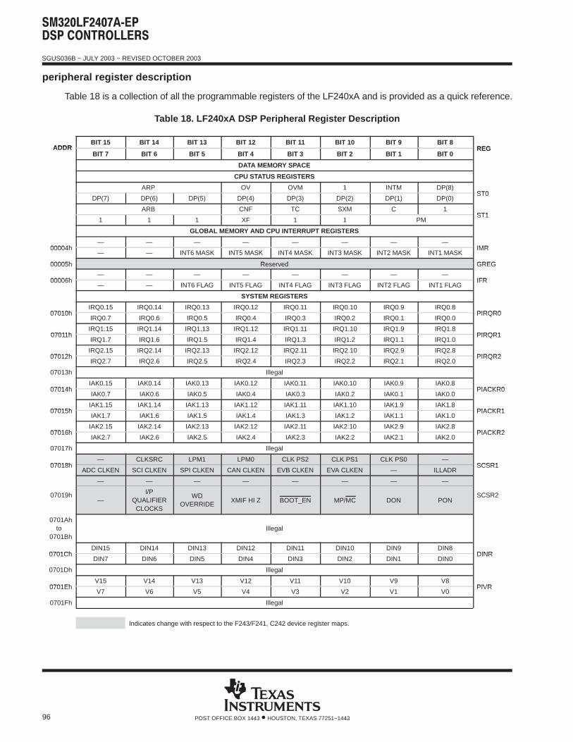
SGUS036B − JULY 2003 − REVISED OCTOBER 2003
96 POST OFFICE BOX 1443 • HOUSTON, TEXAS 77251−1443
peripheral register description
Table 18 is a collection of all the programmable registers of the LF240xA and is provided as a quick reference.
Table 18. LF240xA DSP Peripheral Register Description
ADDRBIT 15 BIT 14 BIT 13 BIT 12 BIT 11 BIT 10 BIT 9 BIT 8
REGADDRBIT 7 BIT 6 BIT 5 BIT 4 BIT 3 BIT 2 BIT 1 BIT 0
REG
DATA MEMORY SPACE
CPU STATUS REGISTERS
ARP OV OVM 1 INTM DP(8)ST0
DP(7) DP(6) DP(5) DP(4) DP(3) DP(2) DP(1) DP(0)ST0
ARB CNF TC SXM C 1ST1
1 1 1 XF 1 1 PMST1
GLOBAL MEMORY AND CPU INTERRUPT REGISTERS
00004h— — — — — — — —
IMR00004h— — INT6 MASK INT5 MASK INT4 MASK INT3 MASK INT2 MASK INT1 MASK
IMR
00005h Reserved GREG00005h Reserved GREG
00006h— — — — — — — —
IFR00006h— — INT6 FLAG INT5 FLAG INT4 FLAG INT3 FLAG INT2 FLAG INT1 FLAG
IFR
SYSTEM REGISTERS
07010hIRQ0.15 IRQ0.14 IRQ0.13 IRQ0.12 IRQ0.11 IRQ0.10 IRQ0.9 IRQ0.8
PIRQR007010hIRQ0.7 IRQ0.6 IRQ0.5 IRQ0.4 IRQ0.3 IRQ0.2 IRQ0.1 IRQ0.0
PIRQR0
07011hIRQ1.15 IRQ1.14 IRQ1.13 IRQ1.12 IRQ1.11 IRQ1.10 IRQ1.9 IRQ1.8
PIRQR107011hIRQ1.7 IRQ1.6 IRQ1.5 IRQ1.4 IRQ1.3 IRQ1.2 IRQ1.1 IRQ1.0
PIRQR1
07012hIRQ2.15 IRQ2.14 IRQ2.13 IRQ2.12 IRQ2.11 IRQ2.10 IRQ2.9 IRQ2.8
PIRQR207012hIRQ2.7 IRQ2.6 IRQ2.5 IRQ2.4 IRQ2.3 IRQ2.2 IRQ2.1 IRQ2.0
PIRQR2
07013h Illegal
07014hIAK0.15 IAK0.14 IAK0.13 IAK0.12 IAK0.11 IAK0.10 IAK0.9 IAK0.8
PIACKR007014hIAK0.7 IAK0.6 IAK0.5 IAK0.4 IAK0.3 IAK0.2 IAK0.1 IAK0.0
PIACKR0
07015hIAK1.15 IAK1.14 IAK1.13 IAK1.12 IAK1.11 IAK1.10 IAK1.9 IAK1.8
PIACKR107015hIAK1.7 IAK1.6 IAK1.5 IAK1.4 IAK1.3 IAK1.2 IAK1.1 IAK1.0
PIACKR1
07016hIAK2.15 IAK2.14 IAK2.13 IAK2.12 IAK2.11 IAK2.10 IAK2.9 IAK2.8
PIACKR207016hIAK2.7 IAK2.6 IAK2.5 IAK2.4 IAK2.3 IAK2.2 IAK2.1 IAK2.0
PIACKR2
07017h Illegal
07018h— CLKSRC LPM1 LPM0 CLK PS2 CLK PS1 CLK PS0 —
SCSR107018hADC CLKEN SCI CLKEN SPI CLKEN CAN CLKEN EVB CLKEN EVA CLKEN — ILLADR
SCSR1
— — — — — — — —
07019h—
I/PQUALIFIER
CLOCKS
WDOVERRIDE
XMIF HI Z BOOT_EN MP/MC DON PONSCSR2
0701Ahto
0701BhIllegal
0701ChDIN15 DIN14 DIN13 DIN12 DIN11 DIN10 DIN9 DIN8
DINR0701ChDIN7 DIN6 DIN5 DIN4 DIN3 DIN2 DIN1 DIN0
DINR
0701Dh Illegal
0701EhV15 V14 V13 V12 V11 V10 V9 V8
PIVR0701EhV7 V6 V5 V4 V3 V2 V1 V0
PIVR
0701Fh Illegal
Indicates change with respect to the F243/F241, C242 device register maps.
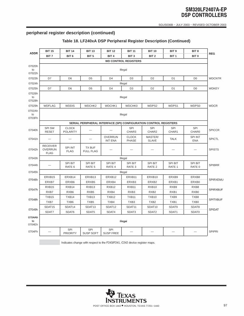
SGUS036B − JULY 2003 − REVISED OCTOBER 2003
97POST OFFICE BOX 1443 • HOUSTON, TEXAS 77251−1443
peripheral register description (continued)
Table 18. LF240xA DSP Peripheral Register Description (Continued)
ADDRBIT 15 BIT 14 BIT 13 BIT 12 BIT 11 BIT 10 BIT 9 BIT 8
REGADDRBIT 7 BIT 6 BIT 5 BIT 4 BIT 3 BIT 2 BIT 1 BIT 0
REG
WD CONTROL REGISTERS
07020hto
07022hIllegal
07023h D7 D6 D5 D4 D3 D2 D1 D0 WDCNTR
07024h Illegal
07025h D7 D6 D5 D4 D3 D2 D1 D0 WDKEY
07026hto
07028hIllegal
07029h WDFLAG WDDIS WDCHK2 WDCHK1 WDCHK0 WDPS2 WDPS1 WDPS0 WDCR
0702Ahto
0703FhIllegal
SERIAL PERIPHERAL INTERFACE (SPI) CONFIGURATION CONTROL REGISTERS
07040hSPI SWRESET
CLOCKPOLARITY
— —SPI
CHAR3SPI
CHAR2SPI
CHAR1SPI
CHAR0SPICCR
07041h — — —OVERRUNINT ENA
CLOCKPHASE
MASTER/SLAVE
TALKSPI INT
ENASPICTL
07042hRECEIVEROVERRUN
FLAG
SPI INTFLAG
TX BUFFULL FLAG
— — — — — SPISTS
07043h Illegal
07044h —SPI BITRATE 6
SPI BITRATE 5
SPI BITRATE 4
SPI BITRATE 3
SPI BITRATE 2
SPI BITRATE 1
SPI BITRATE 0
SPIBRR
07045h Illegal
07046hERXB15 ERXB14 ERXB13 ERXB12 ERXB11 ERXB10 ERXB9 ERXB8
SPIRXEMU07046hERXB7 ERXB6 ERXB5 ERXB4 ERXB3 ERXB2 ERXB1 ERXB0
SPIRXEMU
07047hRXB15 RXB14 RXB13 RXB12 RXB11 RXB10 RXB9 RXB8
SPIRXBUF07047hRXB7 RXB6 RXB5 RXB4 RXB3 RXB2 RXB1 RXB0
SPIRXBUF
07048hTXB15 TXB14 TXB13 TXB12 TXB11 TXB10 TXB9 TXB8
SPITXBUF07048hTXB7 TXB6 TXB5 TXB4 TXB3 TXB2 TXB1 TXB0
SPITXBUF
07049hSDAT15 SDAT14 SDAT13 SDAT12 SDAT11 SDAT10 SDAT9 SDAT8
SPIDAT07049hSDAT7 SDAT6 SDAT5 SDAT4 SDAT3 SDAT2 SDAT1 SDAT0
SPIDAT
0704Ah0704Ahto Illegalto
0704EhIllegal
0704Fh —SPI
PRIORITYSPI
SUSP SOFTSPI
SUSP FREE— — — — SPIPRI
Indicates change with respect to the F243/F241, C242 device register maps.Indicates change with respect to the F243/F241, C242 device register maps.
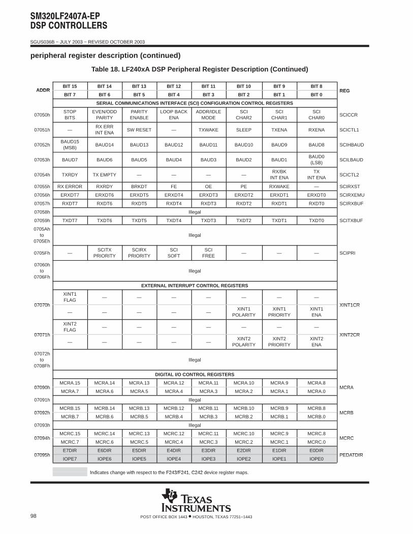
SGUS036B − JULY 2003 − REVISED OCTOBER 2003
98 POST OFFICE BOX 1443 • HOUSTON, TEXAS 77251−1443
peripheral register description (continued)
Table 18. LF240xA DSP Peripheral Register Description (Continued)
ADDRBIT 15 BIT 14 BIT 13 BIT 12 BIT 11 BIT 10 BIT 9 BIT 8
REGADDRBIT 7 BIT 6 BIT 5 BIT 4 BIT 3 BIT 2 BIT 1 BIT 0
REG
SERIAL COMMUNICATIONS INTERFACE (SCI) CONFIGURATION CONTROL REGISTERS
07050hSTOPBITS
EVEN/ODDPARITY
PARITYENABLE
LOOP BACKENA
ADDR/IDLEMODE
SCICHAR2
SCICHAR1
SCICHAR0
SCICCR
07051h —RX ERRINT ENA
SW RESET — TXWAKE SLEEP TXENA RXENA SCICTL1
07052hBAUD15(MSB)
BAUD14 BAUD13 BAUD12 BAUD11 BAUD10 BAUD9 BAUD8 SCIHBAUD
07053h BAUD7 BAUD6 BAUD5 BAUD4 BAUD3 BAUD2 BAUD1BAUD0(LSB)
SCILBAUD
07054h TXRDY TX EMPTY — — — —RX/BK
INT ENATX
INT ENASCICTL2
07055h RX ERROR RXRDY BRKDT FE OE PE RXWAKE — SCIRXST
07056h ERXDT7 ERXDT6 ERXDT5 ERXDT4 ERXDT3 ERXDT2 ERXDT1 ERXDT0 SCIRXEMU
07057h RXDT7 RXDT6 RXDT5 RXDT4 RXDT3 RXDT2 RXDT1 RXDT0 SCIRXBUF
07058h Illegal
07059h TXDT7 TXDT6 TXDT5 TXDT4 TXDT3 TXDT2 TXDT1 TXDT0 SCITXBUF
0705Ahto
0705EhIllegal
0705Fh —SCITX
PRIORITYSCIRX
PRIORITYSCI
SOFTSCI
FREE— — — SCIPRI
07060hto
0706FhIllegal
EXTERNAL INTERRUPT CONTROL REGISTERS
07070h
XINT1FLAG
— — — — — — —
XINT1CR07070h
— — — — —XINT1
POLARITYXINT1
PRIORITYXINT1ENA
XINT1CR
07071h
XINT2FLAG
— — — — — — —
XINT2CR07071h
— — — — —XINT2
POLARITYXINT2
PRIORITYXINT2ENA
XINT2CR
07072hto
0708FhIllegal
DIGITAL I/O CONTROL REGISTERS
07090hMCRA.15 MCRA.14 MCRA.13 MCRA.12 MCRA.11 MCRA.10 MCRA.9 MCRA.8
MCRA07090hMCRA.7 MCRA.6 MCRA.5 MCRA.4 MCRA.3 MCRA.2 MCRA.1 MCRA.0
MCRA
07091h Illegal
07092hMCRB.15 MCRB.14 MCRB.13 MCRB.12 MCRB.11 MCRB.10 MCRB.9 MCRB.8
MCRB07092hMCRB.7 MCRB.6 MCRB.5 MCRB.4 MCRB.3 MCRB.2 MCRB.1 MCRB.0
MCRB
07093h Illegal
07094hMCRC.15 MCRC.14 MCRC.13 MCRC.12 MCRC.11 MCRC.10 MCRC.9 MCRC.8
MCRC07094hMCRC.7 MCRC.6 MCRC.5 MCRC.4 MCRC.3 MCRC.2 MCRC.1 MCRC.0
MCRC
07095hE7DIR E6DIR E5DIR E4DIR E3DIR E2DIR E1DIR E0DIR
PEDATDIR07095hIOPE7 IOPE6 IOPE5 IOPE4 IOPE3 IOPE2 IOPE1 IOPE0
PEDATDIR
Indicates change with respect to the F243/F241, C242 device register maps.Indicates change with respect to the F243/F241, C242 device register maps.
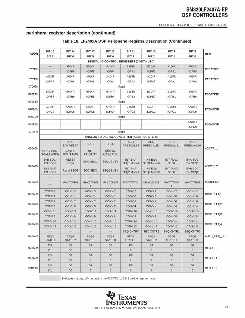
SGUS036B − JULY 2003 − REVISED OCTOBER 2003
99POST OFFICE BOX 1443 • HOUSTON, TEXAS 77251−1443
peripheral register description (continued)
Table 18. LF240xA DSP Peripheral Register Description (Continued)
ADDRBIT 15 BIT 14 BIT 13 BIT 12 BIT 11 BIT 10 BIT 9 BIT 8
REGADDRBIT 7 BIT 6 BIT 5 BIT 4 BIT 3 BIT 2 BIT 1 BIT 0
REG
DIGITAL I/O CONTROL REGISTERS (CONTINUED)
07096h— F6DIR F5DIR F4DIR F3DIR F2DIR F1DIR F0DIR
PFDATDIR07096h— IOPF6 IOPF5 IOPF4 IOPF3 IOPF2 IOPF1 IOPF0
PFDATDIR
07098hA7DIR A6DIR A5DIR A4DIR A3DIR A2DIR A1DIR A0DIR
PADATDIR07098hIOPA7 IOPA6 IOPA5 IOPA4 IOPA3 IOPA2 IOPA1 IOPA0
PADATDIR
07099h Illegal
0709AhB7DIR B6DIR B5DIR B4DIR B3DIR B2DIR B1DIR B0DIR
PBDATDIR0709AhIOPB7 IOPB6 IOPB5 IOPB4 IOPB3 IOPB2 IOPB1 IOPB0
PBDATDIR
0709Bh Illegal
0709ChC7DIR C6DIR C5DIR C4DIR C3DIR C2DIR C1DIR C0DIR
PCDATDIR0709ChIOPC7 IOPC6 IOPC5 IOPC4 IOPC3 IOPC2 IOPC1 IOPC0
PCDATDIR
0709Dh Illegal
0709Eh— — — — — — — D0DIR
PDDATDIR0709Eh— — — — — — — IOPD0
PDDATDIR
0709Fh Illegal
ANALOG-TO-DIGITAL CONVERTER (ADC) REGISTERS
070A0h
—ADC
S/W RESETSOFT FREE
ACQPRESCALE3
ACQPRESCALE2
ACQPRESCALE1
ACQPRESCALE0
ADCTRL1070A0hCONV PRE-
SCALE (CPS)CONTIN-
UOUS RUNINT
PRIORITYSEQ1/2
CASCADE — — — —
ADCTRL1
070A1h
EVB SOC EN SEQ1
RESETSEQ1
SOC SEQ1 SEQ1 BUSYINT ENA
SEQ1 Mode1INT ENA
SEQ1 Mode0INT FLAG
SEQ1EVA SOCEN SEQ1
ADCTRL2070A1hEXT SOCEN SEQ1
Reset SEQ2 SOC SEQ2 SEQ2 BUSYINT ENA
SEQ2 Mode1INT ENA
SEQ2 Mode0INT FLAG
SEQ2EVB SOCEN SEQ2
ADCTRL2
— — — — — — — —
070A2h—
MAXCONV22
MAXCONV21
MAXCONV20
MAXCONV13
MAXCONV12
MAXCONV11
MAXCONV10
MAXCONV
070A3hCONV 3 CONV 3 CONV 3 CONV 3 CONV 2 CONV 2 CONV 2 CONV 2
CHSELSEQ1070A3hCONV 1 CONV 1 CONV 1 CONV 1 CONV 0 CONV 0 CONV 0 CONV 0
CHSELSEQ1
070A4hCONV 7 CONV 7 CONV 7 CONV 7 CONV 6 CONV 6 CONV 6 CONV 6
CHSELSEQ2070A4hCONV 5 CONV 5 CONV 5 CONV 5 CONV 4 CONV 4 CONV 4 CONV 4
CHSELSEQ2
070A5hCONV 11 CONV 11 CONV 11 CONV 11 CONV 10 CONV 10 CONV 10 CONV 10
CHSELSEQ3070A5hCONV 9 CONV 9 CONV 9 CONV 9 CONV 8 CONV 8 CONV 8 CONV 8
CHSELSEQ3
070A6hCONV 15 CONV 15 CONV 15 CONV 15 CONV 14 CONV 14 CONV 14 CONV 14
CHSELSEQ4070A6hCONV 13 CONV 13 CONV 13 CONV 13 CONV 12 CONV 12 CONV 12 CONV 12
CHSELSEQ4
— — — — SEQ CNTR3 SEQ CNTR2 SEQ CNTR1 SEQ CNTR0
070A7h SEQ2STATE 3
SEQ2STATE 2
SEQ2STATE 1
SEQ2STATE 0
SEQ1STATE 3
SEQ1STATE 2
SEQ1STATE 1
SEQ1STATE 0
AUTO_SEQ_SR
070A8hD9 D8 D7 D6 D5 D4 D3 D2
RESULT0070A8hD1 D0 0 0 0 0 0 0
RESULT0
070A9hD9 D8 D7 D6 D5 D4 D3 D2
RESULT1070A9hD1 D0 0 0 0 0 0 0
RESULT1
070AAhD9 D8 D7 D6 D5 D4 D3 D2
RESULT2070AAhD1 D0 0 0 0 0 0 0
RESULT2
Indicates change with respect to the F243/F241, C242 device register maps.Indicates change with respect to the F243/F241, C242 device register maps.
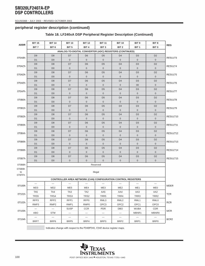
SGUS036B − JULY 2003 − REVISED OCTOBER 2003
100 POST OFFICE BOX 1443 • HOUSTON, TEXAS 77251−1443
peripheral register description (continued)
Table 18. LF240xA DSP Peripheral Register Description (Continued)
ADDRBIT 15 BIT 14 BIT 13 BIT 12 BIT 11 BIT 10 BIT 9 BIT 8
REGADDRBIT 7 BIT 6 BIT 5 BIT 4 BIT 3 BIT 2 BIT 1 BIT 0
REG
ANALOG-TO-DIGITAL CONVERTER (ADC) REGISTERS (CONTINUED)
070ABhD9 D8 D7 D6 D5 D4 D3 D2
RESULT3070ABhD1 D0 0 0 0 0 0 0
RESULT3
070AChD9 D8 D7 D6 D5 D4 D3 D2
RESULT4070AChD1 D0 0 0 0 0 0 0
RESULT4
070ADhD9 D8 D7 D6 D5 D4 D3 D2
RESULT5070ADhD1 D0 0 0 0 0 0 0
RESULT5
070AEhD9 D8 D7 D6 D5 D4 D3 D2
RESULT6070AEhD1 D0 0 0 0 0 00 0
RESULT6
070AFhD9 D8 D7 D6 D5 D4 D3 D2
RESULT7070AFhD1 D0 0 0 0 0 0 0
RESULT7
070B0hD9 D8 D7 D6 D5 D4 D3 D2
RESULT8070B0hD1 D0 0 0 0 0 0 0
RESULT8
070B1hD9 D8 D7 D6 D5 D4 D3 D2
RESULT9070B1hD1 D0 0 0 0 0 0 0
RESULT9
070B2hD9 D8 D7 D6 D5 D4 D3 D2
RESULT10070B2hD1 D0 0 0 0 0 0 0
RESULT10
070B3hD9 D8 D7 D6 D5 D4 D3 D2
RESULT11070B3hD1 D0 0 0 0 0 0 0
RESULT11
070B4hD9 D8 D7 D6 D5 D4 D3 D2
RESULT12070B4hD1 D0 0 0 0 0 0 0
RESULT12
070B5hD9 D8 D7 D6 D5 D4 D3 D2
RESULT13070B5hD1 D0 0 0 0 0 0 0
RESULT13
070B6hD9 D8 D7 D6 D5 D4 D3 D2
RESULT14070B6hD1 D0 0 0 0 0 0 0
RESULT14
070B7hD9 D8 D7 D6 D5 D4 D3 D2
RESULT15070B7hD1 D0 0 0 0 0 0 0
RESULT15
070B8h Reserved
070B9hto
070FFhIllegal
CONTROLLER AREA NETWORK (CAN) CONFIGURATION CONTROL REGISTERS
07100h— — — — — — — —
MDER07100hMD3 MD2 ME5 ME4 ME3 ME2 ME1 ME0
MDER
07101hTA5 TA4 TA3 TA2 AA5 AA4 AA3 AA2
TCR07101hTRS5 TRS4 TRS3 TRS2 TRR5 TRR4 TRR3 TRR2
TCR
07102hRFP3 RFP2 RFP1 RFP0 RML3 RML2 RML1 RML0
RCR07102hRMP3 RMP2 RMP1 RMP0 OPC3 OPC2 OPC1 OPC0
RCR
07103h— — SUSP CCR PDR DBO WUBA CDR
MCR07103hABO STM — — — — MBNR1 MBNR0
MCR
07104h— — — — — — — —
BCR207104hBRP7 BRP6 BRP5 BRP4 BRP3 BRP2 BRP1 BRP0
BCR2
Indicates change with respect to the F243/F241, C242 device register maps.Indicates change with respect to the F243/F241, C242 device register maps.
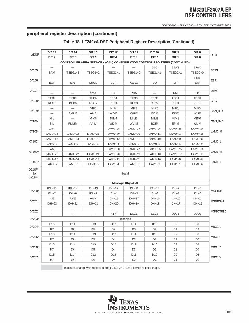
SGUS036B − JULY 2003 − REVISED OCTOBER 2003
101POST OFFICE BOX 1443 • HOUSTON, TEXAS 77251−1443
peripheral register description (continued)
Table 18. LF240xA DSP Peripheral Register Description (Continued)
ADDRBIT 15 BIT 14 BIT 13 BIT 12 BIT 11 BIT 10 BIT 9 BIT 8
REGADDRBIT 7 BIT 6 BIT 5 BIT 4 BIT 3 BIT 2 BIT 1 BIT 0
REG
CONTROLLER AREA NETWORK (CAN) CONFIGURATION CONTROL REGISTERS (CONTINUED)
07105h— — — — — SBG SJW1 SJW0
BCR107105hSAM TSEG1−3 TSEG1−2 TSEG1−1 TSEG1−0 TSEG2−2 TSEG2−1 TSEG2−0
BCR1
07106h— — — — — — — FER
ESR07106hBEF SA1 CRCE SER ACKE BO EP EW
ESR
07107h— — — — — — — —
GSR07107h— — SMA CCE PDA — RM TM
GSR
07108hTEC7 TEC6 TEC5 TEC4 TEC3 TEC2 TEC1 TEC0
CEC07108hREC7 REC6 REC5 REC4 REC3 REC2 REC1 REC0
CEC
07109h— — MIF5 MIF4 MIF3 MIF2 MIF1 MIF0
CAN_IFR07109h— RMLIF AAIF WDIF WUIF BOIF EPIF WLIF
CAN_IFR
0710AhMIL — MIM5 MIM4 MIM3 MIM2 MIM1 MIM0
CAN_IMR0710AhEIL RMLIM AAIM WDIM WUIM BOIM EPIM WLIM
CAN_IMR
0710BhLAMI — — LAM0−28 LAM0−27 LAM0−26 LAM0−25 LAM0−24
LAM0_H0710BhLAM0−23 LAM0−22 LAM0−21 LAM0−20 LAM0−19 LAM0−18 LAM0−17 LAM0−16
LAM0_H
0710ChLAM0−15 LAM0−14 LAM0−13 LAM0−12 LAM0−11 LAM0−10 LAM0−9 LAM0−8
LAM0_L0710ChLAM0−7 LAM0−6 LAM0−5 LAM0−4 LAM0−3 LAM0−2 LAM0−1 LAM0−0
LAM0_L
0710DhLAMI — — LAM1−28 LAM1−27 LAM1−26 LAM1−25 LAM1−24
LAM1_H0710DhLAM1−23 LAM1−22 LAM1−21 LAM1−20 LAM1−19 LAM1−18 LAM1−17 LAM1−16
LAM1_H
0710EhLAM1−15 LAM1−14 LAM1−13 LAM1−12 LAM1−11 LAM1−10 LAM1−9 LAM1−8
LAM1_L0710EhLAM1−7 LAM1−6 LAM1−5 LAM1−4 LAM1−3 LAM1−2 LAM1−1 LAM1−0
LAM1_L
0710Fhto
071FFhIllegal
Message Object #0
07200hIDL−15 IDL−14 IDL−13 IDL−12 IDL−11 IDL−10 IDL−9 IDL−8
MSGID0L07200hIDL−7 IDL−6 IDL−5 IDL−4 IDL−3 IDL−2 IDL−1 IDL−0
MSGID0L
07201hIDE AME AAM IDH−28 IDH−27 IDH−26 IDH−25 IDH−24
MSGID0H07201hIDH−23 IDH−22 IDH−21 IDH−20 IDH−19 IDH−18 IDH−17 IDH−16
MSGID0H
07202h— — — — — — — —
MSGCTRL007202h— — — RTR DLC3 DLC2 DLC1 DLC0
MSGCTRL0
07203h Reserved
07204hD15 D14 D13 D12 D11 D10 D9 D8
MBX0A07204hD7 D6 D5 D4 D3 D2 D1 D0
MBX0A
07205hD15 D14 D13 D12 D11 D10 D9 D8
MBX0B07205hD7 D6 D5 D4 D3 D2 D1 D0
MBX0B
07206hD15 D14 D13 D12 D11 D10 D9 D8
MBX0C07206hD7 D6 D5 D4 D3 D2 D1 D0
MBX0C
07207hD15 D14 D13 D12 D11 D10 D9 D8
MBX0D07207hD7 D6 D5 D4 D3 D2 D1 D0
MBX0D
Indicates change with respect to the F243/F241, C242 device register maps.Indicates change with respect to the F243/F241, C242 device register maps.
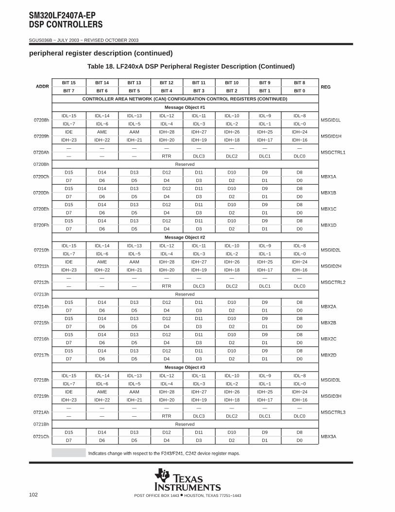
SGUS036B − JULY 2003 − REVISED OCTOBER 2003
102 POST OFFICE BOX 1443 • HOUSTON, TEXAS 77251−1443
peripheral register description (continued)
Table 18. LF240xA DSP Peripheral Register Description (Continued)
ADDRBIT 15 BIT 14 BIT 13 BIT 12 BIT 11 BIT 10 BIT 9 BIT 8
REGADDRBIT 7 BIT 6 BIT 5 BIT 4 BIT 3 BIT 2 BIT 1 BIT 0
REG
CONTROLLER AREA NETWORK (CAN) CONFIGURATION CONTROL REGISTERS (CONTINUED)
Message Object #1
07208hIDL−15 IDL−14 IDL−13 IDL−12 IDL−11 IDL−10 IDL−9 IDL−8
MSGID1L07208hIDL−7 IDL−6 IDL−5 IDL−4 IDL−3 IDL−2 IDL−1 IDL−0
MSGID1L
07209hIDE AME AAM IDH−28 IDH−27 IDH−26 IDH−25 IDH−24
MSGID1H07209hIDH−23 IDH−22 IDH−21 IDH−20 IDH−19 IDH−18 IDH−17 IDH−16
MSGID1H
0720Ah— — — — — — — —
MSGCTRL10720Ah— — — RTR DLC3 DLC2 DLC1 DLC0
MSGCTRL1
0720Bh Reserved
0720ChD15 D14 D13 D12 D11 D10 D9 D8
MBX1A0720ChD7 D6 D5 D4 D3 D2 D1 D0
MBX1A
0720DhD15 D14 D13 D12 D11 D10 D9 D8
MBX1B0720DhD7 D6 D5 D4 D3 D2 D1 D0
MBX1B
0720EhD15 D14 D13 D12 D11 D10 D9 D8
MBX1C0720EhD7 D6 D5 D4 D3 D2 D1 D0
MBX1C
0720FhD15 D14 D13 D12 D11 D10 D9 D8
MBX1D0720FhD7 D6 D5 D4 D3 D2 D1 D0
MBX1D
Message Object #2
07210hIDL−15 IDL−14 IDL−13 IDL−12 IDL−11 IDL−10 IDL−9 IDL−8
MSGID2L07210hIDL−7 IDL−6 IDL−5 IDL−4 IDL−3 IDL−2 IDL−1 IDL−0
MSGID2L
07211hIDE AME AAM IDH−28 IDH−27 IDH−26 IDH−25 IDH−24
MSGID2H07211hIDH−23 IDH−22 IDH−21 IDH−20 IDH−19 IDH−18 IDH−17 IDH−16
MSGID2H
07212h— — — — — — — —
MSGCTRL207212h— — — RTR DLC3 DLC2 DLC1 DLC0
MSGCTRL2
07213h Reserved
07214hD15 D14 D13 D12 D11 D10 D9 D8
MBX2A07214hD7 D6 D5 D4 D3 D2 D1 D0
MBX2A
07215hD15 D14 D13 D12 D11 D10 D9 D8
MBX2B07215hD7 D6 D5 D4 D3 D2 D1 D0
MBX2B
07216hD15 D14 D13 D12 D11 D10 D9 D8
MBX2C07216hD7 D6 D5 D4 D3 D2 D1 D0
MBX2C
07217hD15 D14 D13 D12 D11 D10 D9 D8
MBX2D07217hD7 D6 D5 D4 D3 D2 D1 D0
MBX2D
Message Object #3
07218hIDL−15 IDL−14 IDL−13 IDL−12 IDL−11 IDL−10 IDL−9 IDL−8
MSGID3L07218hIDL−7 IDL−6 IDL−5 IDL−4 IDL−3 IDL−2 IDL−1 IDL−0
MSGID3L
07219hIDE AME AAM IDH−28 IDH−27 IDH−26 IDH−25 IDH−24
MSGID3H07219hIDH−23 IDH−22 IDH−21 IDH−20 IDH−19 IDH−18 IDH−17 IDH−16
MSGID3H
0721Ah— — — — — — — —
MSGCTRL30721Ah— — — RTR DLC3 DLC2 DLC1 DLC0
MSGCTRL3
0721Bh Reserved
0721ChD15 D14 D13 D12 D11 D10 D9 D8
MBX3A0721ChD7 D6 D5 D4 D3 D2 D1 D0
MBX3A
Indicates change with respect to the F243/F241, C242 device register maps.Indicates change with respect to the F243/F241, C242 device register maps.
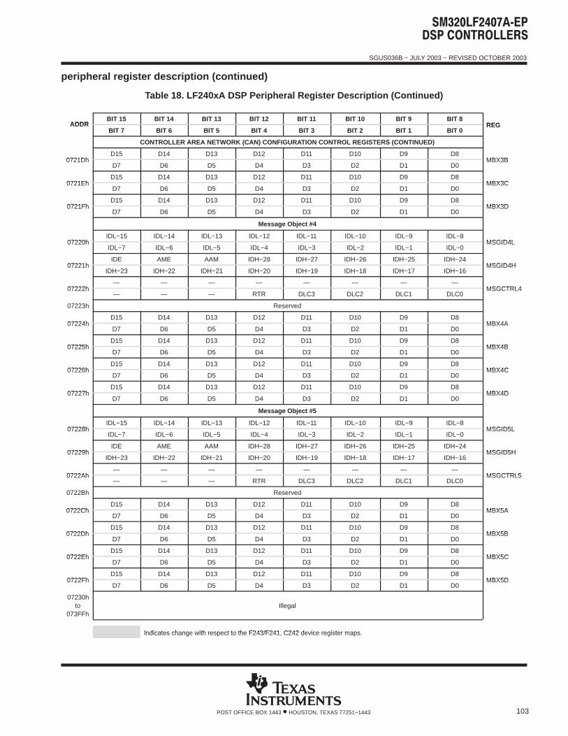
SGUS036B − JULY 2003 − REVISED OCTOBER 2003
103POST OFFICE BOX 1443 • HOUSTON, TEXAS 77251−1443
peripheral register description (continued)
Table 18. LF240xA DSP Peripheral Register Description (Continued)
ADDRBIT 15 BIT 14 BIT 13 BIT 12 BIT 11 BIT 10 BIT 9 BIT 8
REGADDRBIT 7 BIT 6 BIT 5 BIT 4 BIT 3 BIT 2 BIT 1 BIT 0
REG
CONTROLLER AREA NETWORK (CAN) CONFIGURATION CONTROL REGISTERS (CONTINUED)
0721DhD15 D14 D13 D12 D11 D10 D9 D8
MBX3B0721DhD7 D6 D5 D4 D3 D2 D1 D0
MBX3B
0721EhD15 D14 D13 D12 D11 D10 D9 D8
MBX3C0721EhD7 D6 D5 D4 D3 D2 D1 D0
MBX3C
0721FhD15 D14 D13 D12 D11 D10 D9 D8
MBX3D0721FhD7 D6 D5 D4 D3 D2 D1 D0
MBX3D
Message Object #4
07220hIDL−15 IDL−14 IDL−13 IDL−12 IDL−11 IDL−10 IDL−9 IDL−8
MSGID4L07220hIDL−7 IDL−6 IDL−5 IDL−4 IDL−3 IDL−2 IDL−1 IDL−0
MSGID4L
07221hIDE AME AAM IDH−28 IDH−27 IDH−26 IDH−25 IDH−24
MSGID4H07221hIDH−23 IDH−22 IDH−21 IDH−20 IDH−19 IDH−18 IDH−17 IDH−16
MSGID4H
07222h— — — — — — — —
MSGCTRL407222h— — — RTR DLC3 DLC2 DLC1 DLC0
MSGCTRL4
07223h Reserved
07224hD15 D14 D13 D12 D11 D10 D9 D8
MBX4A07224hD7 D6 D5 D4 D3 D2 D1 D0
MBX4A
07225hD15 D14 D13 D12 D11 D10 D9 D8
MBX4B07225hD7 D6 D5 D4 D3 D2 D1 D0
MBX4B
07226hD15 D14 D13 D12 D11 D10 D9 D8
MBX4C07226hD7 D6 D5 D4 D3 D2 D1 D0
MBX4C
07227hD15 D14 D13 D12 D11 D10 D9 D8
MBX4D07227hD7 D6 D5 D4 D3 D2 D1 D0
MBX4D
Message Object #5
07228hIDL−15 IDL−14 IDL−13 IDL−12 IDL−11 IDL−10 IDL−9 IDL−8
MSGID5L07228hIDL−7 IDL−6 IDL−5 IDL−4 IDL−3 IDL−2 IDL−1 IDL−0
MSGID5L
07229hIDE AME AAM IDH−28 IDH−27 IDH−26 IDH−25 IDH−24
MSGID5H07229hIDH−23 IDH−22 IDH−21 IDH−20 IDH−19 IDH−18 IDH−17 IDH−16
MSGID5H
0722Ah— — — — — — — —
MSGCTRL50722Ah— — — RTR DLC3 DLC2 DLC1 DLC0
MSGCTRL5
0722Bh Reserved
0722ChD15 D14 D13 D12 D11 D10 D9 D8
MBX5A0722ChD7 D6 D5 D4 D3 D2 D1 D0
MBX5A
0722DhD15 D14 D13 D12 D11 D10 D9 D8
MBX5B0722DhD7 D6 D5 D4 D3 D2 D1 D0
MBX5B
0722EhD15 D14 D13 D12 D11 D10 D9 D8
MBX5C0722EhD7 D6 D5 D4 D3 D2 D1 D0
MBX5C
0722FhD15 D14 D13 D12 D11 D10 D9 D8
MBX5D0722FhD7 D6 D5 D4 D3 D2 D1 D0
MBX5D
07230hto
073FFhIllegal
Indicates change with respect to the F243/F241, C242 device register maps.Indicates change with respect to the F243/F241, C242 device register maps.
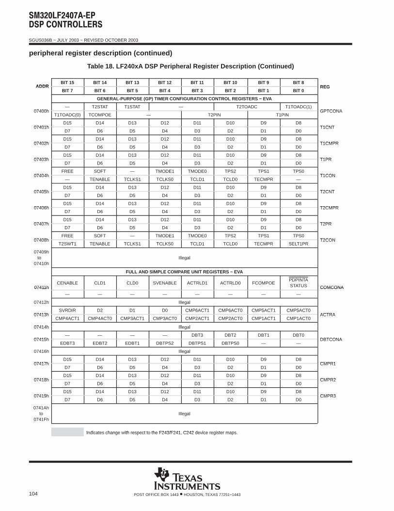
SGUS036B − JULY 2003 − REVISED OCTOBER 2003
104 POST OFFICE BOX 1443 • HOUSTON, TEXAS 77251−1443
peripheral register description (continued)
Table 18. LF240xA DSP Peripheral Register Description (Continued)
ADDRBIT 15 BIT 14 BIT 13 BIT 12 BIT 11 BIT 10 BIT 9 BIT 8
REGADDRBIT 7 BIT 6 BIT 5 BIT 4 BIT 3 BIT 2 BIT 1 BIT 0
REG
GENERAL-PURPOSE (GP) TIMER CONFIGURATION CONTROL REGISTERS − EVA
07400h— T2STAT T1STAT — T2TOADC T1TOADC(1)
GPTCONA07400hT1TOADC(0) TCOMPOE — T2PIN T1PIN
GPTCONA
07401hD15 D14 D13 D12 D11 D10 D9 D8
T1CNT07401hD7 D6 D5 D4 D3 D2 D1 D0
T1CNT
07402hD15 D14 D13 D12 D11 D10 D9 D8
T1CMPR07402hD7 D6 D5 D4 D3 D2 D1 D0
T1CMPR
07403hD15 D14 D13 D12 D11 D10 D9 D8
T1PR07403hD7 D6 D5 D4 D3 D2 D1 D0
T1PR
07404hFREE SOFT — TMODE1 TMODE0 TPS2 TPS1 TPS0
T1CON07404h— TENABLE TCLKS1 TCLKS0 TCLD1 TCLD0 TECMPR —
T1CON
07405hD15 D14 D13 D12 D11 D10 D9 D8
T2CNT07405hD7 D6 D5 D4 D3 D2 D1 D0
T2CNT
07406hD15 D14 D13 D12 D11 D10 D9 D8
T2CMPR07406hD7 D6 D5 D4 D3 D2 D1 D0
T2CMPR
07407hD15 D14 D13 D12 D11 D10 D9 D8
T2PR07407hD7 D6 D5 D4 D3 D2 D1 D0
T2PR
07408hFREE SOFT — TMODE1 TMODE0 TPS2 TPS1 TPS0
T2CON07408hT2SWT1 TENABLE TCLKS1 TCLKS0 TCLD1 TCLD0 TECMPR SELT1PR
T2CON
07409hto
07410hIllegal
FULL AND SIMPLE COMPARE UNIT REGISTERS − EVA
07411hCENABLE CLD1 CLD0 SVENABLE ACTRLD1 ACTRLD0 FCOMPOE
PDPINTASTATUS COMCONA07411h
— — — — — — — —
COMCONA
07412h Illegal
07413hSVRDIR D2 D1 D0 CMP6ACT1 CMP6ACT0 CMP5ACT1 CMP5ACT0
ACTRA07413hCMP4ACT1 CMP4ACT0 CMP3ACT1 CMP3ACT0 CMP2ACT1 CMP2ACT0 CMP1ACT1 CMP1ACT0
ACTRA
07414h Illegal07414h Illegal
07415h— — — — DBT3 DBT2 DBT1 DBT0
DBTCONA07415hEDBT3 EDBT2 EDBT1 DBTPS2 DBTPS1 DBTPS0 — —
DBTCONA
07416h Illegal
07417hD15 D14 D13 D12 D11 D10 D9 D8
CMPR107417hD7 D6 D5 D4 D3 D2 D1 D0
CMPR1
07418hD15 D14 D13 D12 D11 D10 D9 D8
CMPR207418hD7 D6 D5 D4 D3 D2 D1 D0
CMPR2
07419hD15 D14 D13 D12 D11 D10 D9 D8
CMPR307419hD7 D6 D5 D4 D3 D2 D1 D0
CMPR3
0741Ahto
0741FhIllegal
Indicates change with respect to the F243/F241, C242 device register maps.Indicates change with respect to the F243/F241, C242 device register maps.
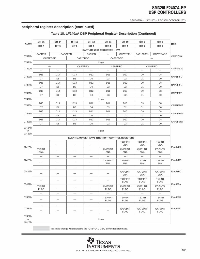
SGUS036B − JULY 2003 − REVISED OCTOBER 2003
105POST OFFICE BOX 1443 • HOUSTON, TEXAS 77251−1443
peripheral register description (continued)
Table 18. LF240xA DSP Peripheral Register Description (Continued)
ADDRBIT 15 BIT 14 BIT 13 BIT 12 BIT 11 BIT 10 BIT 9 BIT 8
REGADDRBIT 7 BIT 6 BIT 5 BIT 4 BIT 3 BIT 2 BIT 1 BIT 0
REG
CAPTURE UNIT REGISTERS − EVA
07420hCAPRES CAPQEPN CAP3EN — CAP3TSEL CAP12TSEL CAP3TOADC
CAPCONA07420hCAP1EDGE CAP2EDGE CAP3EDGE —
CAPCONA
07421h Illegal
07422h— CAP3FIFO CAP2FIFO CAP1FIFO
CAPFIFOA07422h— — — — — — — —
CAPFIFOA
07423hD15 D14 D13 D12 D11 D10 D9 D8
CAP1FIFO07423hD7 D6 D5 D4 D3 D2 D1 D0
CAP1FIFO
07424hD15 D14 D13 D12 D11 D10 D9 D8
CAP2FIFO07424hD7 D6 D5 D4 D3 D2 D1 D0
CAP2FIFO
07425hD15 D14 D13 D12 D11 D10 D9 D8
CAP3FIFO07425hD7 D6 D5 D4 D3 D2 D1 D0
CAP3FIFO
07426h Illegal
07427hD15 D14 D13 D12 D11 D10 D9 D8
CAP1FBOT07427hD7 D6 D5 D4 D3 D2 D1 D0
CAP1FBOT
07428hD15 D14 D13 D12 D11 D10 D9 D8
CAP2FBOT07428hD7 D6 D5 D4 D3 D2 D1 D0
CAP2FBOT
07429hD15 D14 D13 D12 D11 D10 D9 D8
CAP3FBOT07429hD7 D6 D5 D4 D3 D2 D1 D0
CAP3FBOT
0742Ahto
0742BhIllegal
EVENT MANAGER (EVA) INTERRUPT CONTROL REGISTERS
0742Ch
— — — — —T1OFINT
ENAT1UFINT
ENAT1CINT
ENAEVAIMRA0742Ch
T1PINTENA
— — —CMP3INT
ENACMP2INT
ENACMP1INT
ENAPDPINTA
ENA
EVAIMRA
— — — — — — — —
0742Dh— — — —
T2OFINTENA
T2UFINTENA
T2CINTENA
T2PINTENA
EVAIMRB
— — — — — — — —
0742Eh— — — — —
CAP3INTENA
CAP2INTENA
CAP1INTENA
EVAIMRC
0742Fh
— — — — —T1OFINT
FLAGT1UFINT
FLAGT1CINTFLAG
EVAIFRA0742FhT1PINTFLAG
— — —CMP3INT
FLAGCMP2INT
FLAGCMP1INT
FLAGPDPINTA
FLAG
EVAIFRA
— — — — — — — —
07430h— — — —
T2OFINTFLAG
T2UFINTFLAG
T2CINTFLAG
T2PINTFLAG
EVAIFRB
— — — — — — — —
07431h— — — — —
CAP3INTFLAG
CAP2INTFLAG
CAP1INTFLAG
EVAIFRC
07432hto
074FFhIllegal
Indicates change with respect to the F243/F241, C242 device register maps.Indicates change with respect to the F243/F241, C242 device register maps.
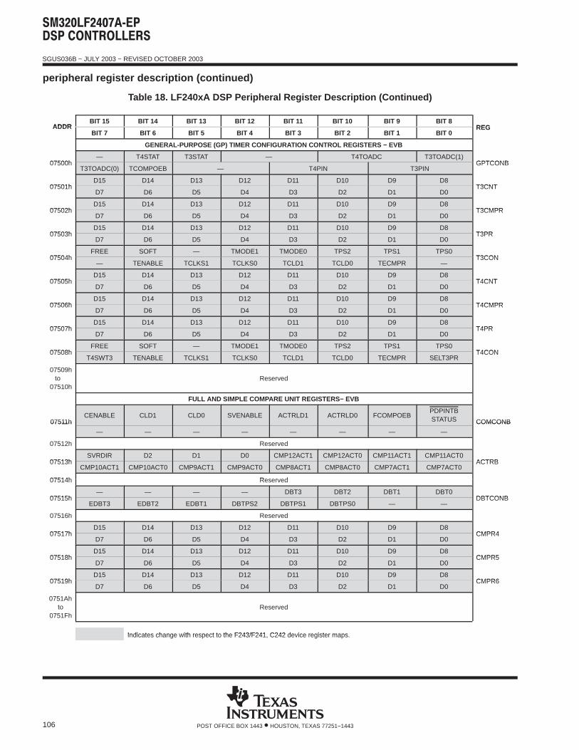
SGUS036B − JULY 2003 − REVISED OCTOBER 2003
106 POST OFFICE BOX 1443 • HOUSTON, TEXAS 77251−1443
peripheral register description (continued)
Table 18. LF240xA DSP Peripheral Register Description (Continued)
ADDRBIT 15 BIT 14 BIT 13 BIT 12 BIT 11 BIT 10 BIT 9 BIT 8
REGADDRBIT 7 BIT 6 BIT 5 BIT 4 BIT 3 BIT 2 BIT 1 BIT 0
REG
GENERAL-PURPOSE (GP) TIMER CONFIGURATION CONTROL REGISTERS − EVB
07500h— T4STAT T3STAT — T4TOADC T3TOADC(1)
GPTCONB07500hT3TOADC(0) TCOMPOEB — T4PIN T3PIN
GPTCONB
07501hD15 D14 D13 D12 D11 D10 D9 D8
T3CNT07501hD7 D6 D5 D4 D3 D2 D1 D0
T3CNT
07502hD15 D14 D13 D12 D11 D10 D9 D8
T3CMPR07502hD7 D6 D5 D4 D3 D2 D1 D0
T3CMPR
07503hD15 D14 D13 D12 D11 D10 D9 D8
T3PR07503hD7 D6 D5 D4 D3 D2 D1 D0
T3PR
07504hFREE SOFT — TMODE1 TMODE0 TPS2 TPS1 TPS0
T3CON07504h— TENABLE TCLKS1 TCLKS0 TCLD1 TCLD0 TECMPR —
T3CON
07505hD15 D14 D13 D12 D11 D10 D9 D8
T4CNT07505hD7 D6 D5 D4 D3 D2 D1 D0
T4CNT
07506hD15 D14 D13 D12 D11 D10 D9 D8
T4CMPR07506hD7 D6 D5 D4 D3 D2 D1 D0
T4CMPR
07507hD15 D14 D13 D12 D11 D10 D9 D8
T4PR07507hD7 D6 D5 D4 D3 D2 D1 D0
T4PR
07508hFREE SOFT — TMODE1 TMODE0 TPS2 TPS1 TPS0
T4CON07508hT4SWT3 TENABLE TCLKS1 TCLKS0 TCLD1 TCLD0 TECMPR SELT3PR
T4CON
07509hto
07510hReserved
FULL AND SIMPLE COMPARE UNIT REGISTERS− EVB
07511hCENABLE CLD1 CLD0 SVENABLE ACTRLD1 ACTRLD0 FCOMPOEB
PDPINTBSTATUS COMCONB07511h
— — — — — — — —
COMCONB
07512h Reserved
07513hSVRDIR D2 D1 D0 CMP12ACT1 CMP12ACT0 CMP11ACT1 CMP11ACT0
ACTRB07513hCMP10ACT1 CMP10ACT0 CMP9ACT1 CMP9ACT0 CMP8ACT1 CMP8ACT0 CMP7ACT1 CMP7ACT0
ACTRB
07514h Reserved07514h Reserved
07515h— — — — DBT3 DBT2 DBT1 DBT0
DBTCONB07515hEDBT3 EDBT2 EDBT1 DBTPS2 DBTPS1 DBTPS0 — —
DBTCONB
07516h Reserved
07517hD15 D14 D13 D12 D11 D10 D9 D8
CMPR407517hD7 D6 D5 D4 D3 D2 D1 D0
CMPR4
07518hD15 D14 D13 D12 D11 D10 D9 D8
CMPR507518hD7 D6 D5 D4 D3 D2 D1 D0
CMPR5
07519hD15 D14 D13 D12 D11 D10 D9 D8
CMPR607519hD7 D6 D5 D4 D3 D2 D1 D0
CMPR6
0751Ahto
0751FhReserved
Indicates change with respect to the F243/F241, C242 device register maps.Indicates change with respect to the F243/F241, C242 device register maps.
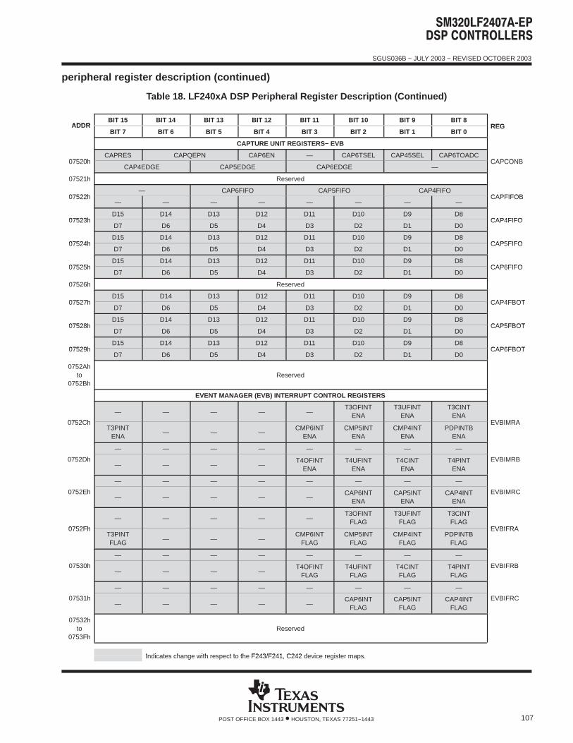
SGUS036B − JULY 2003 − REVISED OCTOBER 2003
107POST OFFICE BOX 1443 • HOUSTON, TEXAS 77251−1443
peripheral register description (continued)
Table 18. LF240xA DSP Peripheral Register Description (Continued)
ADDRBIT 15 BIT 14 BIT 13 BIT 12 BIT 11 BIT 10 BIT 9 BIT 8
REGADDRBIT 7 BIT 6 BIT 5 BIT 4 BIT 3 BIT 2 BIT 1 BIT 0
REG
CAPTURE UNIT REGISTERS− EVB
07520hCAPRES CAPQEPN CAP6EN — CAP6TSEL CAP45SEL CAP6TOADC
CAPCONB07520hCAP4EDGE CAP5EDGE CAP6EDGE —
CAPCONB
07521h Reserved
07522h— CAP6FIFO CAP5FIFO CAP4FIFO
CAPFIFOB07522h— — — — — — — —
CAPFIFOB
07523hD15 D14 D13 D12 D11 D10 D9 D8
CAP4FIFO07523hD7 D6 D5 D4 D3 D2 D1 D0
CAP4FIFO
07524hD15 D14 D13 D12 D11 D10 D9 D8
CAP5FIFO07524hD7 D6 D5 D4 D3 D2 D1 D0
CAP5FIFO
07525hD15 D14 D13 D12 D11 D10 D9 D8
CAP6FIFO07525hD7 D6 D5 D4 D3 D2 D1 D0
CAP6FIFO
07526h Reserved
07527hD15 D14 D13 D12 D11 D10 D9 D8
CAP4FBOT07527hD7 D6 D5 D4 D3 D2 D1 D0
CAP4FBOT
07528hD15 D14 D13 D12 D11 D10 D9 D8
CAP5FBOT07528hD7 D6 D5 D4 D3 D2 D1 D0
CAP5FBOT
07529hD15 D14 D13 D12 D11 D10 D9 D8
CAP6FBOT07529hD7 D6 D5 D4 D3 D2 D1 D0
CAP6FBOT
0752Ahto
0752BhReserved
EVENT MANAGER (EVB) INTERRUPT CONTROL REGISTERS
0752Ch
— — — — —T3OFINT
ENAT3UFINT
ENAT3CINT
ENAEVBIMRA0752Ch
T3PINTENA
— — —CMP6INT
ENACMP5INT
ENACMP4INT
ENAPDPINTB
ENA
EVBIMRA
— — — — — — — —
0752Dh— — — —
T4OFINTENA
T4UFINTENA
T4CINTENA
T4PINTENA
EVBIMRB
— — — — — — — —
0752Eh— — — — —
CAP6INTENA
CAP5INTENA
CAP4INTENA
EVBIMRC
0752Fh
— — — — —T3OFINT
FLAGT3UFINT
FLAGT3CINTFLAG
EVBIFRA0752FhT3PINTFLAG
— — —CMP6INT
FLAGCMP5INT
FLAGCMP4INT
FLAGPDPINTB
FLAG
EVBIFRA
— — — — — — — —
07530h— — — —
T4OFINTFLAG
T4UFINTFLAG
T4CINTFLAG
T4PINTFLAG
EVBIFRB
— — — — — — — —
07531h— — — — —
CAP6INTFLAG
CAP5INTFLAG
CAP4INTFLAG
EVBIFRC
07532hto
0753FhReserved
Indicates change with respect to the F243/F241, C242 device register maps.Indicates change with respect to the F243/F241, C242 device register maps.
SGUS036B − JULY 2003 − REVISED OCTOBER 2003
108 POST OFFICE BOX 1443 • HOUSTON, TEXAS 77251−1443
peripheral register description (continued)
Table 18. LF240xA DSP Peripheral Register Description (Continued)
ADDRBIT 15 BIT 14 BIT 13 BIT 12 BIT 11 BIT 10 BIT 9 BIT 8
REGADDRBIT 7 BIT 6 BIT 5 BIT 4 BIT 3 BIT 2 BIT 1 BIT 0
REG
KEY REGISTERS
077F0h High Word of the 64-Bit KEY Register KEY3077F0h High Word of the 64-Bit KEY Register KEY3
077F1h Third Word of the 64-Bit KEY Register KEY2077F1h Third Word of the 64-Bit KEY Register KEY2
077F2h Second Word of the 64-Bit KEY Register KEY1077F2h Second Word of the 64-Bit KEY Register KEY1
077F3h Low Word of the 64-Bit KEY Register KEY0077F3h Low Word of the 64-Bit KEY Register KEY0
PROGRAM MEMORY SPACE − FLASH REGISTERS
0xx00h— — — — — — — —
PMPC0xx00h— — — — PWR DWN KEY1 KEY0 EXEC
PMPC
0xx01h
— — — — — — WSVER ENPRECND
Mode1CTRL†0xx01h
PRECNDMode0
ENG/RMode2
ENG/RMode1
ENG/RMode0
FCM3 FCM2 FCM1 FCM0
CTRL†
0xx02h WADDR0xx02h WADDR
0xx03h WDATA0xx03h WDATA
0xx04h— — — — — — — —
TCR0xx04h— — — — — — — —
TCR
0xx05h— — — — — — — —
ENAB0xx05h— — — — — — — —
ENAB
— — — — — — — —
0xx06h— — — —
SECT 4ENABLE
SECT 3ENABLE
SECT 2ENABLE
SECT 1ENABLE
SECT
I/O MEMORY SPACE
0FF0Fh— — — — — — — —
FCMR0FF0Fh— — — — — — — —
FCMR
WAIT-STATE GENERATOR CONTROL REGISTER
0FFFFh— — — — — BVIS.1 BVIS.0 ISWS.2
WSGR0FFFFhISWS.1 ISWS.0 DSWS.2 DSWS.1 DSWS.0 PSWS.2 PSWS.1 PSWS.0
WSGR
Indicates change with respect to the F243/F241, C242 device register maps.Indicates change with respect to the F243/F241, C242 device register maps.
† Register shown with bits set in register mode .
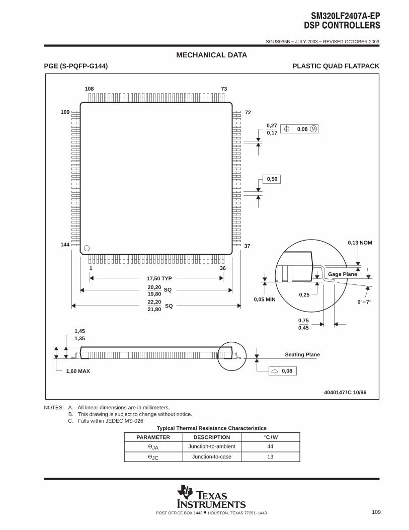
SGUS036B − JULY 2003 − REVISED OCTOBER 2003
109POST OFFICE BOX 1443 • HOUSTON, TEXAS 77251−1443
MECHANICAL DATAPGE (S-PQFP-G144) PLASTIC QUAD FLATPACK
4040147/C 10/96
0,27
72
0,17
37
73
0,13 NOM
0,25
0,750,45
0,05 MIN
36
Seating Plane
Gage Plane
108
109
144
SQ
SQ22,2021,80
1
19,80
17,50 TYP
20,20
1,351,45
1,60 MAX
M0,08
0°−7°
0,08
0,50
NOTES: A. All linear dimensions are in millimeters.B. This drawing is subject to change without notice.C. Falls within JEDEC MS-026
Typical Thermal Resistance Characteristics
PARAMETER DESCRIPTION °C/W
ΘJA Junction-to-ambient 44
ΘJC Junction-to-case 13
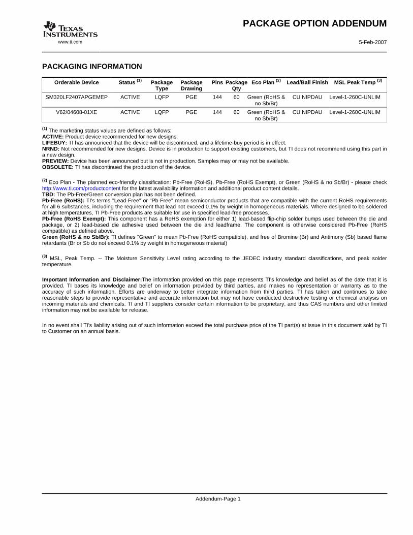
PACKAGING INFORMATION
Orderable Device Status (1) PackageType
PackageDrawing
Pins PackageQty
Eco Plan (2) Lead/Ball Finish MSL Peak Temp (3)
SM320LF2407APGEMEP ACTIVE LQFP PGE 144 60 Green (RoHS &no Sb/Br)
CU NIPDAU Level-1-260C-UNLIM
V62/04608-01XE ACTIVE LQFP PGE 144 60 Green (RoHS &no Sb/Br)
CU NIPDAU Level-1-260C-UNLIM
(1) The marketing status values are defined as follows:ACTIVE: Product device recommended for new designs.LIFEBUY: TI has announced that the device will be discontinued, and a lifetime-buy period is in effect.NRND: Not recommended for new designs. Device is in production to support existing customers, but TI does not recommend using this part ina new design.PREVIEW: Device has been announced but is not in production. Samples may or may not be available.OBSOLETE: TI has discontinued the production of the device.
(2) Eco Plan - The planned eco-friendly classification: Pb-Free (RoHS), Pb-Free (RoHS Exempt), or Green (RoHS & no Sb/Br) - please checkhttp://www.ti.com/productcontent for the latest availability information and additional product content details.TBD: The Pb-Free/Green conversion plan has not been defined.Pb-Free (RoHS): TI's terms "Lead-Free" or "Pb-Free" mean semiconductor products that are compatible with the current RoHS requirementsfor all 6 substances, including the requirement that lead not exceed 0.1% by weight in homogeneous materials. Where designed to be solderedat high temperatures, TI Pb-Free products are suitable for use in specified lead-free processes.Pb-Free (RoHS Exempt): This component has a RoHS exemption for either 1) lead-based flip-chip solder bumps used between the die andpackage, or 2) lead-based die adhesive used between the die and leadframe. The component is otherwise considered Pb-Free (RoHScompatible) as defined above.Green (RoHS & no Sb/Br): TI defines "Green" to mean Pb-Free (RoHS compatible), and free of Bromine (Br) and Antimony (Sb) based flameretardants (Br or Sb do not exceed 0.1% by weight in homogeneous material)
(3) MSL, Peak Temp. -- The Moisture Sensitivity Level rating according to the JEDEC industry standard classifications, and peak soldertemperature.
Important Information and Disclaimer:The information provided on this page represents TI's knowledge and belief as of the date that it isprovided. TI bases its knowledge and belief on information provided by third parties, and makes no representation or warranty as to theaccuracy of such information. Efforts are underway to better integrate information from third parties. TI has taken and continues to takereasonable steps to provide representative and accurate information but may not have conducted destructive testing or chemical analysis onincoming materials and chemicals. TI and TI suppliers consider certain information to be proprietary, and thus CAS numbers and other limitedinformation may not be available for release.
In no event shall TI's liability arising out of such information exceed the total purchase price of the TI part(s) at issue in this document sold by TIto Customer on an annual basis.
PACKAGE OPTION ADDENDUM
www.ti.com 5-Feb-2007
Addendum-Page 1
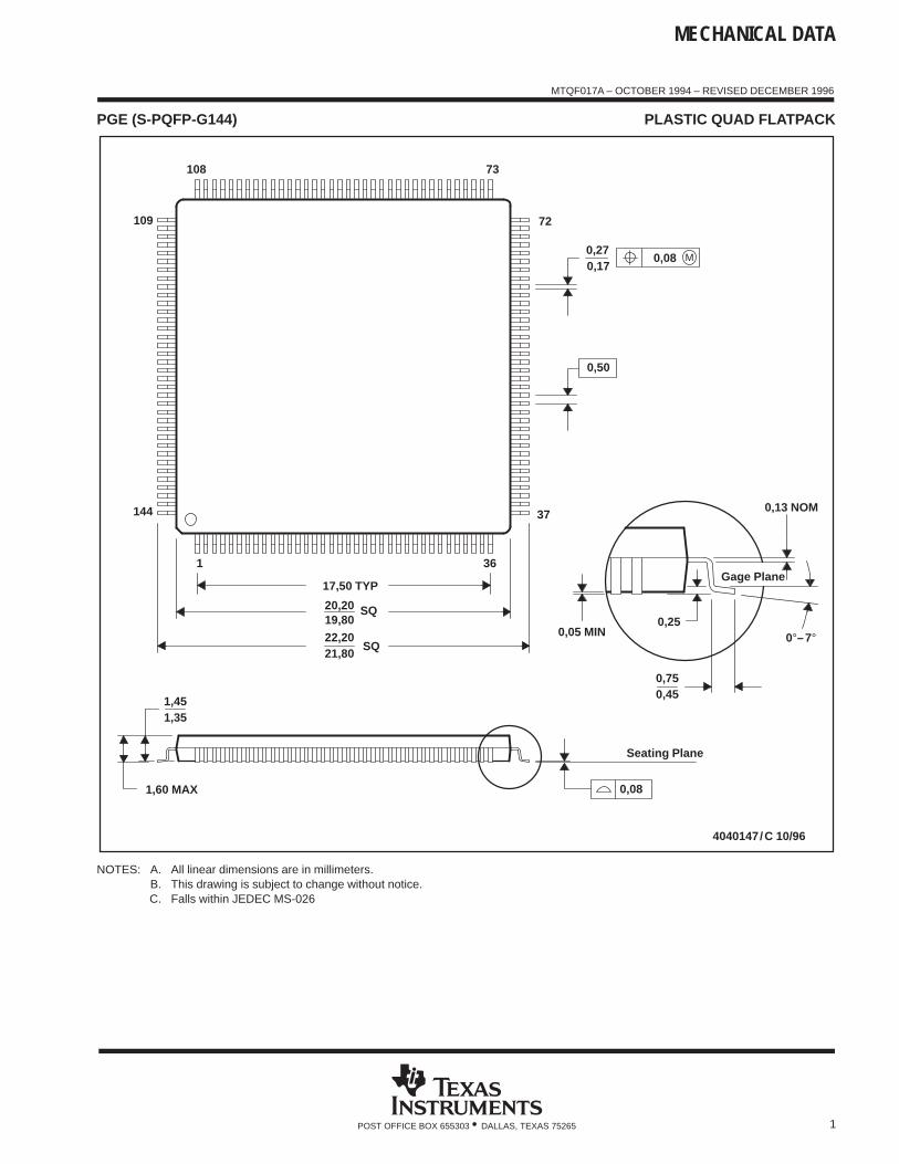
MECHANICAL DATA
MTQF017A – OCTOBER 1994 – REVISED DECEMBER 1996
1POST OFFICE BOX 655303 • DALLAS, TEXAS 75265
PGE (S-PQFP-G144) PLASTIC QUAD FLATPACK
4040147/C 10/96
0,27
72
0,17
37
73
0,13 NOM
0,25
0,750,45
0,05 MIN
36
Seating Plane
Gage Plane
108
109
144
SQ
SQ22,2021,80
1
19,80
17,50 TYP
20,20
1,351,45
1,60 MAX
M0,08
0°–7°
0,08
0,50
NOTES: A. All linear dimensions are in millimeters.B. This drawing is subject to change without notice.C. Falls within JEDEC MS-026
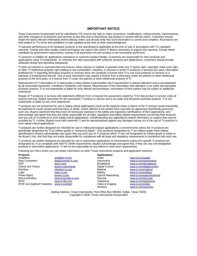
IMPORTANT NOTICETexas Instruments Incorporated and its subsidiaries (TI) reserve the right to make corrections, modifications, enhancements, improvements,and other changes to its products and services at any time and to discontinue any product or service without notice. Customers shouldobtain the latest relevant information before placing orders and should verify that such information is current and complete. All products aresold subject to TI’s terms and conditions of sale supplied at the time of order acknowledgment.TI warrants performance of its hardware products to the specifications applicable at the time of sale in accordance with TI’s standardwarranty. Testing and other quality control techniques are used to the extent TI deems necessary to support this warranty. Except wheremandated by government requirements, testing of all parameters of each product is not necessarily performed.TI assumes no liability for applications assistance or customer product design. Customers are responsible for their products andapplications using TI components. To minimize the risks associated with customer products and applications, customers should provideadequate design and operating safeguards.TI does not warrant or represent that any license, either express or implied, is granted under any TI patent right, copyright, mask work right,or other TI intellectual property right relating to any combination, machine, or process in which TI products or services are used. Informationpublished by TI regarding third-party products or services does not constitute a license from TI to use such products or services or awarranty or endorsement thereof. Use of such information may require a license from a third party under the patents or other intellectualproperty of the third party, or a license from TI under the patents or other intellectual property of TI.Reproduction of TI information in TI data books or data sheets is permissible only if reproduction is without alteration and is accompaniedby all associated warranties, conditions, limitations, and notices. Reproduction of this information with alteration is an unfair and deceptivebusiness practice. TI is not responsible or liable for such altered documentation. Information of third parties may be subject to additionalrestrictions.Resale of TI products or services with statements different from or beyond the parameters stated by TI for that product or service voids allexpress and any implied warranties for the associated TI product or service and is an unfair and deceptive business practice. TI is notresponsible or liable for any such statements.TI products are not authorized for use in safety-critical applications (such as life support) where a failure of the TI product would reasonablybe expected to cause severe personal injury or death, unless officers of the parties have executed an agreement specifically governingsuch use. Buyers represent that they have all necessary expertise in the safety and regulatory ramifications of their applications, andacknowledge and agree that they are solely responsible for all legal, regulatory and safety-related requirements concerning their productsand any use of TI products in such safety-critical applications, notwithstanding any applications-related information or support that may beprovided by TI. Further, Buyers must fully indemnify TI and its representatives against any damages arising out of the use of TI products insuch safety-critical applications.TI products are neither designed nor intended for use in military/aerospace applications or environments unless the TI products arespecifically designated by TI as military-grade or "enhanced plastic." Only products designated by TI as military-grade meet militaryspecifications. Buyers acknowledge and agree that any such use of TI products which TI has not designated as military-grade is solely atthe Buyer's risk, and that they are solely responsible for compliance with all legal and regulatory requirements in connection with such use.TI products are neither designed nor intended for use in automotive applications or environments unless the specific TI products aredesignated by TI as compliant with ISO/TS 16949 requirements. Buyers acknowledge and agree that, if they use any non-designatedproducts in automotive applications, TI will not be responsible for any failure to meet such requirements.Following are URLs where you can obtain information on other Texas Instruments products and application solutions:Products ApplicationsAmplifiers amplifier.ti.com Audio www.ti.com/audioData Converters dataconverter.ti.com Automotive www.ti.com/automotiveDSP dsp.ti.com Broadband www.ti.com/broadbandClocks and Timers www.ti.com/clocks Digital Control www.ti.com/digitalcontrolInterface interface.ti.com Medical www.ti.com/medicalLogic logic.ti.com Military www.ti.com/militaryPower Mgmt power.ti.com Optical Networking www.ti.com/opticalnetworkMicrocontrollers microcontroller.ti.com Security www.ti.com/securityRFID www.ti-rfid.com Telephony www.ti.com/telephonyRF/IF and ZigBee® Solutions www.ti.com/lprf Video & Imaging www.ti.com/video
Wireless www.ti.com/wireless
Mailing Address: Texas Instruments, Post Office Box 655303, Dallas, Texas 75265Copyright © 2008, Texas Instruments Incorporated