Embed Size (px)
Citation preview
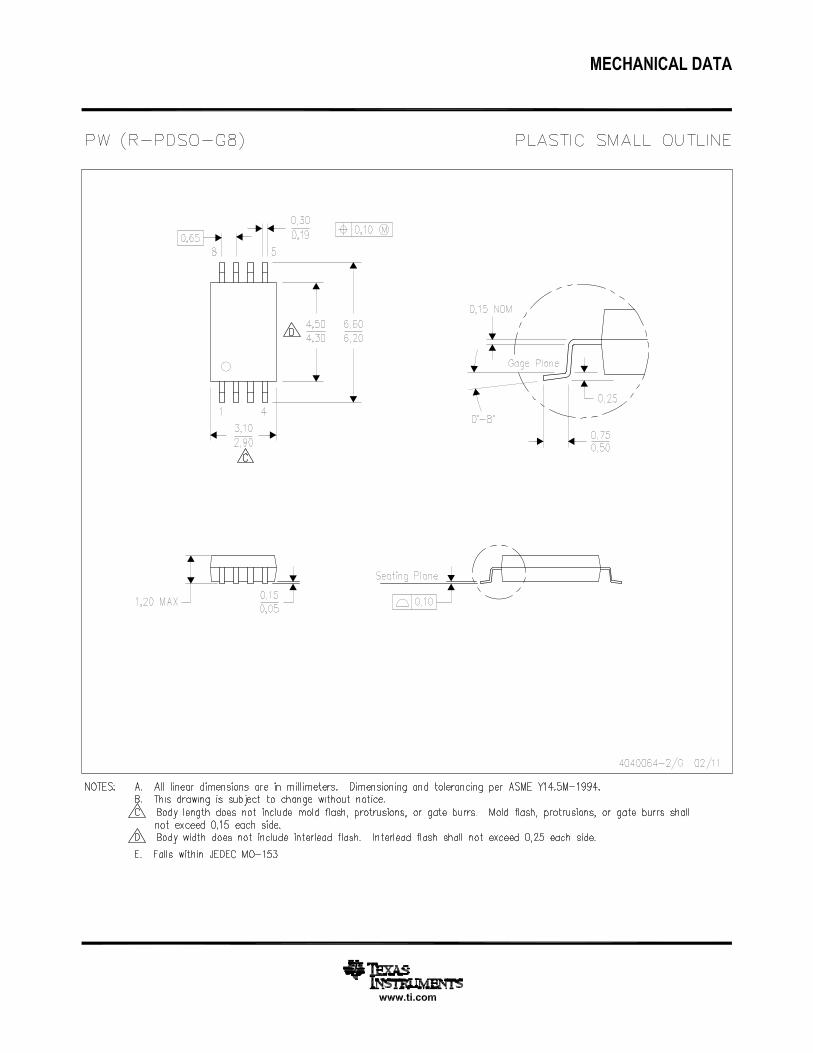
8
REF
3
FB COMP CS
12
4
7
6
5
VoltageReference
REFOK
LogicPower
0.5 V
VCCOK
4 V
1.5 V
Over Current REF/2
Full CycleSoft Start
S Q
RS Q
R
T Q
Oscillator
Leading EdgeBlanking
PWMLatch
UCCx813-1UCCx813-4UCCx813-5
Only
13.5 V
1Vτ=4ms
VCC
OUT
GND
S Q
R
UCC2813-0, UCC2813-1, UCC2813-2, UCC2813-3, UCC2813-4, UCC2813-5UCC3813-0, UCC3813-1, UCC3813-2, UCC3813-3, UCC3813-4, UCC3813-5
www.ti.com SLUS161D –APRIL 1999–REVISED JUNE 2013
Low-Power Economy BiCMOS Current-Mode PWMCheck for Samples: UCC2813-0, UCC2813-1, UCC2813-2, UCC2813-3, UCC2813-4, UCC2813-5, UCC3813-0, UCC3813-1, UCC3813-
2, UCC3813-3, UCC3813-4, UCC3813-5
1FEATURES DESCRIPTIONThe UCC3813-x family of high-speed, low-power• 100-µA Typical Starting Supply Currentintegrated circuits contain all of the control and drive• 500-µA Typical Operating Supply Current components required for off-line and DC-to-DC fixed-
• Operation to 1 MHz frequency current-mode switching power supplieswith minimal parts count.• Internal Soft Start
• Internal Fault Soft Start These devices have the same pin configuration asthe UC384x family, and also offer the added features• Internal Leading-Edge Blanking of the Current-of internal full-cycle soft start and internal leading-Sense Signaledge blanking of the current-sense input.
• 1-A Totem-Pole OutputThe UCC3813-x family offers a variety of package• 70-ns Typical Response from Current-Sense to options, temperature-range options, choice ofGate-Drive Output maximum duty cycle, and choice of critical voltage
• 1.5% Tolerance Voltage Reference levels. Lower reference parts such as the UCC3813-3and UCC38135 fit best into battery operated systems,• Same Pinout as UCC3802, UC3842, andwhile the higher reference and the higher UVLOUC3842Ahysteresis of the UCC3813-2 and UCC3813-4 makethese ideal choices for use in off-line power supplies.
The UCC2813-x series is specified for operation from–40°C to +85°C and the UCC3813-x series isspecified for operation from 0°C to 70°C.
BLOCK DIAGRAM
1
Please be aware that an important notice concerning availability, standard warranty, and use in critical applications ofTexas Instruments semiconductor products and disclaimers thereto appears at the end of this data sheet.
PRODUCTION DATA information is current as of publication date. Copyright © 1999–2013, Texas Instruments IncorporatedProducts conform to specifications per the terms of the TexasInstruments standard warranty. Production processing does notnecessarily include testing of all parameters.
UCC2813-0, UCC2813-1, UCC2813-2, UCC2813-3, UCC2813-4, UCC2813-5UCC3813-0, UCC3813-1, UCC3813-2, UCC3813-3, UCC3813-4, UCC3813-5SLUS161D –APRIL 1999–REVISED JUNE 2013 www.ti.com
This integrated circuit can be damaged by ESD. Texas Instruments recommends that all integrated circuits be handled withappropriate precautions. Failure to observe proper handling and installation procedures can cause damage.
ESD damage can range from subtle performance degradation to complete device failure. Precision integrated circuits may be moresusceptible to damage because very small parametric changes could cause the device not to meet its published specifications.
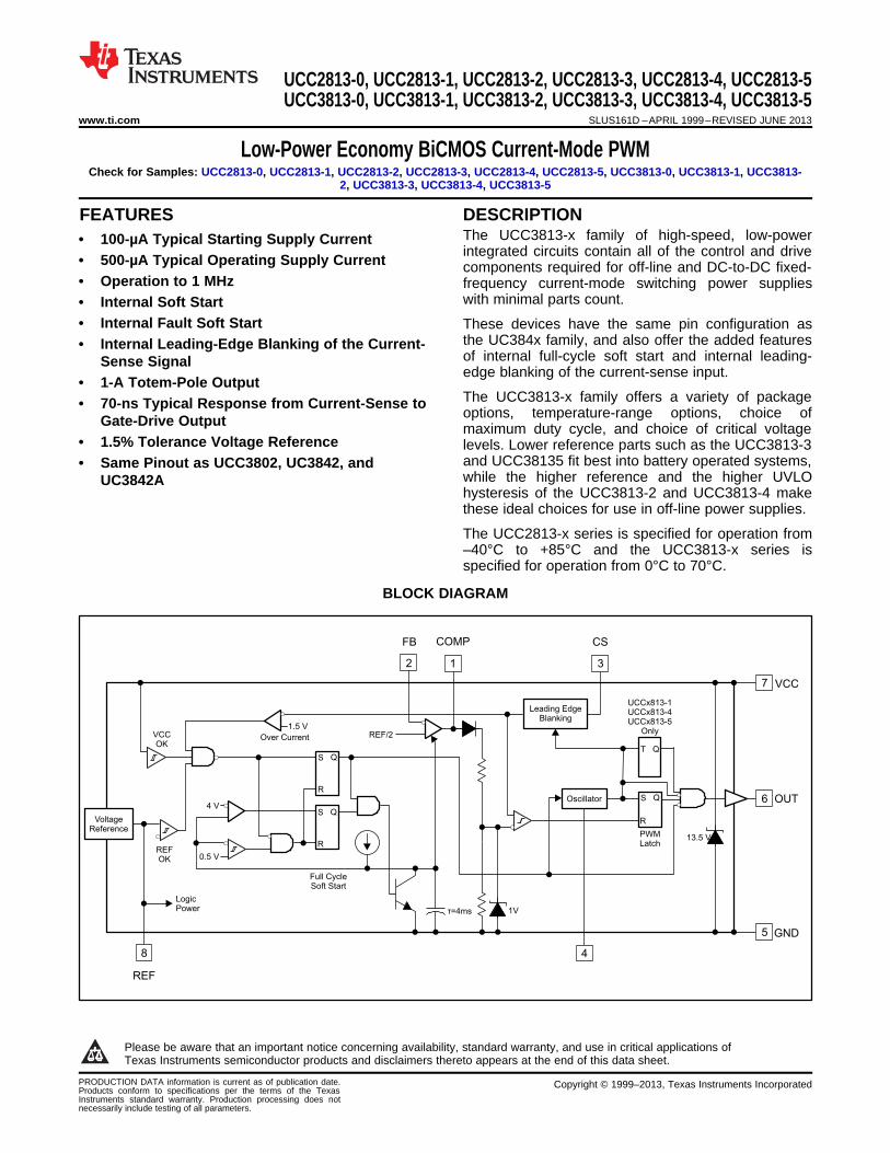
Part Number (1) Maximum Duty Cycle Reference Voltage Turn-On Threshold Turn-Off ThresholdUCCx813-0 100% 5 V 7.2 V 6.9 VUCCx813-1 50% 5 V 9.4 V 7.4 VUCCx813-2 100% 5 V 12.5 V 8.3 VUCCx813-3 100% 4 V 4.1 V 3.6 VUCCx813-4 50% 5 V 12.5 V 8.3 VUCCx813-5 50% 4 V 4.1 V 3.6 V
(1) The x in the part number refers to temperature range difference between UCC2813 and UCC3813.
ABSOLUTE MAXIMUM RATINGS (1) (2)
over operating free-air temperature range (unless otherwise noted)MIN MAX UNIT
Analog inputs (FB, CS, RC, COMP) –3 to the lesser of 6.3 or VCC + 0.3 VVCC voltage (3) 12 VOUT current ±1 AVCC current 30 mAOUT energy (capacitive load) 20 µJPower dissipation at TA < 25°C D package 0.65 W
N package 1 WJunction temperature –55 150 °CStorage temperature –65 150 °C
(1) All voltages are with respect to GND. All currents are positive into the specified terminal. Consult Unitrode Integrated Circuits databookfor Information regarding thermal specifications and limitations of packages.
(2) Stresses beyond those listed under absolute maximum ratings may cause permanent damage to the device. These are stress ratingsonly, and functional operation of the device at these or any other conditions beyond those indicated under recommended operatingconditions is not implied. Exposure to absolute-maximum-rated conditions for extended periods may affect device reliability.
(3) In normal operation VCC is powered through a current limiting resistor. Absolute maximum of 12 V applies when VCC is driven from alow impedance source such that ICC does not exceed 30 mA. The resistor must be sized so that the VCC voltage under-operatingconditions is below 12 V but above the tunoff threshold.
Thermal InformationUCCX813-X UCCX813-X UCCX813-X
THERMAL METRIC (1) DIL (P) SOIC (D) TSSOP (PW) UNITS8 PINS 8 PINS 8 PINS
θJA Junction-to-ambient thermal resistance (2) 50.9 107.5 153.8θJCtop Junction-to-case (top) thermal resistance (3) 40.3 49.3 38.4θJB Junction-to-board thermal resistance (4) 28.1 48.7 83.8 °C/WψJT Junction-to-top characterization parameter (5) 17.6 6.6 2.2ψJB Junction-to-board characterization parameter (6) 28.0 48.0 82.0
(1) For more information about traditional and new thermal metrics, see the IC Package Thermal Metrics application report, SPRA953.(2) The junction-to-ambient thermal resistance under natural convection is obtained in a simulation on a JEDEC-standard, high-K board, as
specified in JESD51-7, in an environment described in JESD51-2a.(3) The junction-to-case (top) thermal resistance is obtained by simulating a cold plate test on the package top. No specific JEDEC-
standard test exists, but a close description can be found in the ANSI SEMI standard G30-88.(4) The junction-to-board thermal resistance is obtained by simulating in an environment with a ring cold plate fixture to control the PCB
temperature, as described in JESD51-8.(5) The junction-to-top characterization parameter, ψJT, estimates the junction temperature of a device in a real system and is extracted
from the simulation data for obtaining θJA, using a procedure described in JESD51-2a (sections 6 and 7).(6) The junction-to-board characterization parameter, ψJB, estimates the junction temperature of a device in a real system and is extracted
from the simulation data for obtaining θJA , using a procedure described in JESD51-2a (sections 6 and 7).
2 Submit Documentation Feedback Copyright © 1999–2013, Texas Instruments Incorporated
Product Folder Links: UCC2813-0 UCC2813-1 UCC2813-2 UCC2813-3 UCC2813-4 UCC2813-5 UCC3813-0UCC3813-1 UCC3813-2 UCC3813-3 UCC3813-4 UCC3813-5
COMPCS
CS
VA 0 V 0.8 V
V
D= £ £
D(5) Gain is defined by: .
UCC2813-0, UCC2813-1, UCC2813-2, UCC2813-3, UCC2813-4, UCC2813-5UCC3813-0, UCC3813-1, UCC3813-2, UCC3813-3, UCC3813-4, UCC3813-5
www.ti.com SLUS161D –APRIL 1999–REVISED JUNE 2013
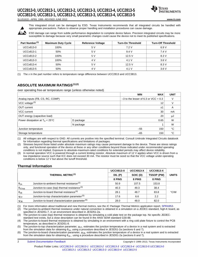
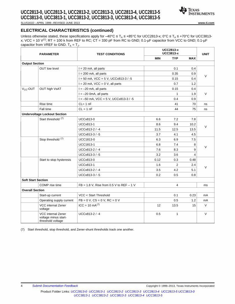
ELECTRICAL CHARACTERISTICSUnless otherwise stated, these specifications apply for –40°C ≤ TA ≤ +85°C for UCC2813-x; 0°C ≤ TA ≤ +70°C for UCC3813-x; VCC = 10 V (1); RT = 100 k from REF to RC; CT = 330 pF from RC to GND; 0.1-µF capacitor from VCC to GND; 0.1-µFcapacitor from VREF to GND. TA = TJ.
UCC2813-xUCC3813-xPARAMETER TEST CONDITIONS UNIT
MIN TYP MAXReference Section
Output voltage TJ = 25°C, I = 0.2 mA, UCCx813-0 / -1 / -2 / -4 4.925 5 5.075V
TJ = 25°C, I = 0.2 mA, UCCx813-3 / -5 3.94 4 4.06Load regulation 0.2 mA < I < 5 mA 10 30 mVTotal variation UCCx813-0 / -1 / -2 / -4 (2) 4.84 5 5.1
VUCCx813-5, UCCx813-3 (2) 3.84 4 4.08
Output noise voltage 10 Hz ≤ f ≤ 10 kHz, TJ = 25°C (3) 70 µVLong term stability TA = 125°C, 1000 Hours (3) 5 mVOutput short circuit –5 –35 mA
Oscillator SectionOscillator frequency UCCx813-0 / -1 / -2 / -4 (4) 40 46 52
kHZUCCx813-3 / -5 (4) 26 31 36
Temperature stability See (3) 2.5 %Amplitude peak-to-peak 2.25 2.4 2.55 VOscillator peak voltage 2.45 V
Error Amplifier SectionInput voltage COMP = 2.5 V; UCCx813-0 / -1 / -2 / -4 2.42 2.5 2.56
VCOMP = 2 V; UCCx813-3 / -5 1.92 2 2.05
Input bias current –2 2 µAOpen loop voltage gain 60 80 dBCOMP sink current FB = 2.7 V, COMP = 1.1 V 0.4 2.5 mACOMP source current FB = 1.8 V, COMP = REF – 1.2 V –0.2 –0.5 –0.8 mAGain bandwidth product See (3) 2 MHZ
PWM SectionMaximum duty cycle UCCx813-0 / -2 / -3 97 99 100
%UCCx813-1 / -4 / -5 48 49 50
Minimum duty cycle COMP = 0 V 0 %Current Sense Section
Gain See (5) 1.1 1.65 1.8 V/VMaximum input signal COMP = 5 V (6) 0.9 1 1.1 VInput bias current –200 200 nACS blank time 50 100 150 nsovercurrent threshold 1.32 1.55 1.7 VCOMP to CS offset CS = 0 V 0.45 0.9 1.35 V
(1) Adjust VCC above the start threshold before setting at 10 V.(2) Total Variation includes temperature stability and load regulation.(3) Ensured by design. Not 100% tested in production.(4) Oscillator frequency for the UCCx813-0, UCCx813-2, and UCCx813-3 is the output frequency.
Oscillator frequency for the UCCx813-1, UCCx813-4, and UCCx813-5 is twice the output frequency.
(6) Parameter measured at trip point of latch with Pin 2 at 0 V.
Copyright © 1999–2013, Texas Instruments Incorporated Submit Documentation Feedback 3
Product Folder Links: UCC2813-0 UCC2813-1 UCC2813-2 UCC2813-3 UCC2813-4 UCC2813-5 UCC3813-0UCC3813-1 UCC3813-2 UCC3813-3 UCC3813-4 UCC3813-5
UCC2813-0, UCC2813-1, UCC2813-2, UCC2813-3, UCC2813-4, UCC2813-5UCC3813-0, UCC3813-1, UCC3813-2, UCC3813-3, UCC3813-4, UCC3813-5SLUS161D –APRIL 1999–REVISED JUNE 2013 www.ti.com
ELECTRICAL CHARACTERISTICS (continued)Unless otherwise stated, these specifications apply for –40°C ≤ TA ≤ +85°C for UCC2813-x; 0°C ≤ TA ≤ +70°C for UCC3813-x; VCC = 10 V(1); RT = 100 k from REF to RC; CT = 330 pF from RC to GND; 0.1-µF capacitor from VCC to GND; 0.1-µFcapacitor from VREF to GND. TA = TJ.
UCC2813-xUCC3813-xPARAMETER TEST CONDITIONS UNIT
MIN TYP MAXOutput Section
OUT low level I = 20 mA, all parts 0.1 0.4I = 200 mA, all parts 0.35 0.9
VI = 50 mA, VCC = 5 V, UCCx813-3 / -5 0.15 0.4I = 20 mA, VCC = 0 V, all parts 0.7 1.2
VCC-OUT OUT high VsAT I = –20 mA, all parts 0.15 0.4I = –20 0mA, all parts 1 1.9 VI = –50 mA, VCC = 5 V, UCCx813-3 / -5 0.4 0.9
Rise time CL= 1 nF 41 70 nsFall time CL = 1 nF 44 75 ns
Undervoltage Lockout SectionStart threshold (7) UCCx813-0 6.6 7.2 7.8
UCCx813-1 8.6 9.4 10.2V
UCCx813-2 / -4 11.5 12.5 13.5UCCx813-3 / -5 3.7 4.1 4.5
Stop threshold (7) UCC1813-0 6.3 6.9 7.5UCC1813-1 6.8 7.4 8
VUCCx813-2 / -4 7.6 8.3 9UCCx813-3 / -5 3.2 3.6 4
Start to stop hysteresis UCCx813-0 0.12 0.3 0.48UCCx813-1 1.6 2 2.4
VUCCx813-2 / -4 3.5 4.2 5.1UCCx813-3 / -5 0.2 0.5 0.8
Soft Start SectionCOMP rise time FB = 1.8 V, Rise from 0.5 V to REF – 1 V 4 ms
Overall SectionStart-up current VCC < Start Threshold 0.1 0.23 mAOperating supply current FB = 0 V, CS = 0 V, RC = 0 V 0.5 1.2 mAVCC internal Zener ICC = 10 mA (7) 12 13.5 15 VvoltageVCC internal Zener UCCx813-2 / -4 0.5 1 Vvoltage minus start-threshold voltage
(7) Start threshold, stop threshold, and Zener-shunt thresholds track one another.
4 Submit Documentation Feedback Copyright © 1999–2013, Texas Instruments Incorporated
Product Folder Links: UCC2813-0 UCC2813-1 UCC2813-2 UCC2813-3 UCC2813-4 UCC2813-5 UCC3813-0UCC3813-1 UCC3813-2 UCC3813-3 UCC3813-4 UCC3813-5
OUT
VCC
REF
GND
FB
COMP
CS
RC
1
2
3
4
8
7
6
5
COMP
FB
CS
RC
REF
VCC
OUT
GND
8
7
6
5
1
2
3
4
UCC2813-0, UCC2813-1, UCC2813-2, UCC2813-3, UCC2813-4, UCC2813-5UCC3813-0, UCC3813-1, UCC3813-2, UCC3813-3, UCC3813-4, UCC3813-5
www.ti.com SLUS161D –APRIL 1999–REVISED JUNE 2013
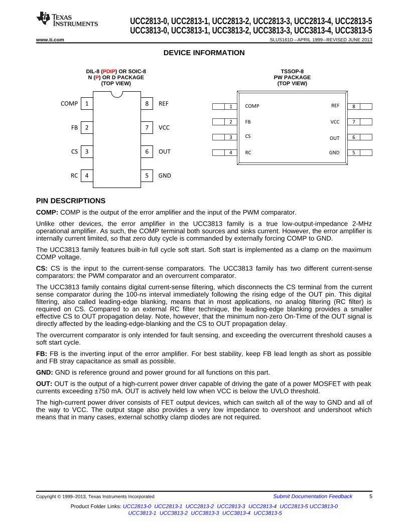
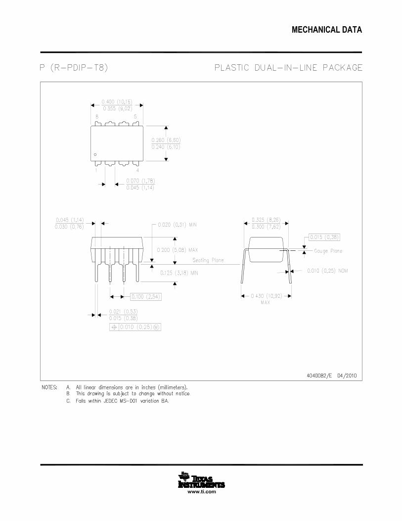
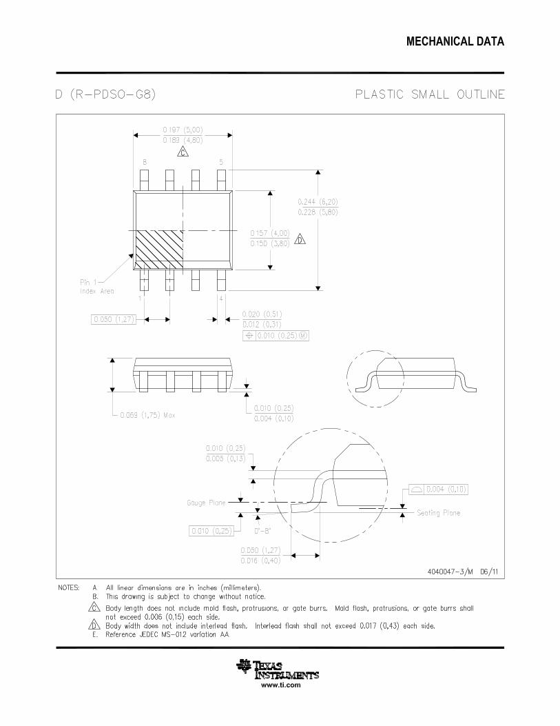
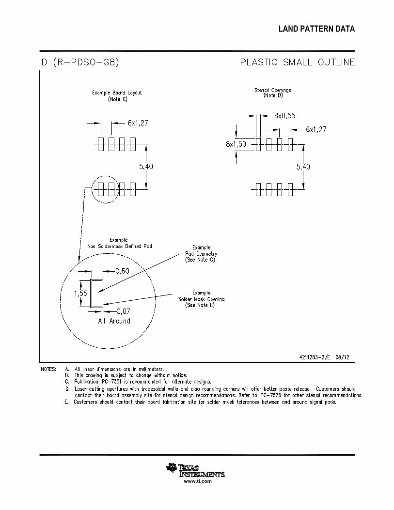
DEVICE INFORMATION
DIL-8 (PDIP) OR SOIC-8 TSSOP-8N (P) OR D PACKAGE PW PACKAGE
(TOP VIEW) (TOP VIEW)
PIN DESCRIPTIONSCOMP: COMP is the output of the error amplifier and the input of the PWM comparator.
Unlike other devices, the error amplifier in the UCC3813 family is a true low-output-impedance 2-MHzoperational amplifier. As such, the COMP terminal both sources and sinks current. However, the error amplifier isinternally current limited, so that zero duty cycle is commanded by externally forcing COMP to GND.
The UCC3813 family features built-in full cycle soft start. Soft start is implemented as a clamp on the maximumCOMP voltage.
CS: CS is the input to the current-sense comparators. The UCC3813 family has two different current-sensecomparators: the PWM comparator and an overcurrent comparator.
The UCC3813 family contains digital current-sense filtering, which disconnects the CS terminal from the currentsense comparator during the 100-ns interval immediately following the rising edge of the OUT pin. This digitalfiltering, also called leading-edge blanking, means that in most applications, no analog filtering (RC filter) isrequired on CS. Compared to an external RC filter technique, the leading-edge blanking provides a smallereffective CS to OUT propagation delay. Note, however, that the minimum non-zero On-Time of the OUT signal isdirectly affected by the leading-edge-blanking and the CS to OUT propagation delay.
The overcurrent comparator is only intended for fault sensing, and exceeding the overcurrent threshold causes asoft start cycle.
FB: FB is the inverting input of the error amplifier. For best stability, keep FB lead length as short as possibleand FB stray capacitance as small as possible.
GND: GND is reference ground and power ground for all functions on this part.
OUT: OUT is the output of a high-current power driver capable of driving the gate of a power MOSFET with peakcurrents exceeding ±750 mA. OUT is actively held low when VCC is below the UVLO threshold.
The high-current power driver consists of FET output devices, which can switch all of the way to GND and all ofthe way to VCC. The output stage also provides a very low impedance to overshoot and undershoot whichmeans that in many cases, external schottky clamp diodes are not required.
Copyright © 1999–2013, Texas Instruments Incorporated Submit Documentation Feedback 5
Product Folder Links: UCC2813-0 UCC2813-1 UCC2813-2 UCC2813-3 UCC2813-4 UCC2813-5 UCC3813-0UCC3813-1 UCC3813-2 UCC3813-3 UCC3813-4 UCC3813-5
1.5UCCx813 0 / 1/ 2 / 4 : F
R C
1UCCx813 3, UCCx813 5 : F
R C
- - - - =´
- - =´
UCC2813-0, UCC2813-1, UCC2813-2, UCC2813-3, UCC2813-4, UCC2813-5UCC3813-0, UCC3813-1, UCC3813-2, UCC3813-3, UCC3813-4, UCC3813-5SLUS161D –APRIL 1999–REVISED JUNE 2013 www.ti.com
RC: RC is the oscillator timing pin. For fixed frequency operation, set the timing-capacitor charging current byconnecting a resistor from REF to RC. Set frequency by connecting a timing capacitor from RC to GND. For bestperformance, keep the timing capacitor lead to GND as short and direct as possible. If possible, use separateground traces for the timing capacitor and all other functions.
The frequency of oscillation is estimated with the following equations:
where• frequency is in hertz• resistance is in ohms• capacitance is in farads (1)
The recommended range of timing resistors is between 10 and 200 k and timing capacitor is 100 to 1000 pF.Never use a timing resistor less than 10 k.
REF: REF is the voltage reference for the error amplifier and also for many other functions on the IC. REF is alsoused as the logic power supply for high speed switching logic on the IC.
When VCC is greater than 1 V and less than the UVLO threshold, REF is pulled to ground through a 5-kQresistor which means that REF is used as a logic output indicating power-system status. For referencing stability,bypassing REF to GND with a ceramic capacitor as close to the pin as possible is important. An electrolyticcapacitor is also used in addition to the ceramic capacitor. A minimum of 0.1-µF ceramic is required. AdditionalREF bypassing is required for external loads greater than 2.5 mA on the reference.
To prevent noise problems with high speed switching transients, bypass REF to ground with a ceramic capacitorvery close to the IC package.
VCC: VCC is the power input connection for this device. In normal operation VCC is powered through a currentlimiting resistor. Although quiescent VCC current is very low, total supply current will be higher, depending onOUT current. Total VCC current is the sum of quiescent VCC current and the average OUT current. Knowing theoperating frequency and the MOSFET gate charge (Qg), average OUT current can be calculated fromEquation 2.
IOUT = Qg × F (2)
To prevent noise problems, bypass VCC to GND with a 0.1-µF ceramic capacitor in parallel as close to the VCCpin as possible. An electrolytic capacitor can also be used in addition to the ceramic capacitor.
6 Submit Documentation Feedback Copyright © 1999–2013, Texas Instruments Incorporated
Product Folder Links: UCC2813-0 UCC2813-1 UCC2813-2 UCC2813-3 UCC2813-4 UCC2813-5 UCC3813-0UCC3813-1 UCC3813-2 UCC3813-3 UCC3813-4 UCC3813-5
4.00
3.98
3.96
3.94
3.92
3.90
3.88
3.86
3.84
3.82
4 4.2 4.4 4.6 4.8 5 5.2 5.4 5.6 5.8 6
V (V)CC
V(V
)R
EF
0
45
90
135
-20
0
20
40
60
80
10k 10k 100k 1M 10M
Phase
(º)
Gain
(dB
)
Frequency (Hz)
C001
Phase
Gain
_
+8REF
4
S
QR
_
+
RC
CT
RT
0.2 V
2.5 V
UCC2813-0, UCC2813-1, UCC2813-2, UCC2813-3, UCC2813-4, UCC2813-5UCC3813-0, UCC3813-1, UCC3813-2, UCC3813-3, UCC3813-4, UCC3813-5
www.ti.com SLUS161D –APRIL 1999–REVISED JUNE 2013
APPLICATION INFORMATION
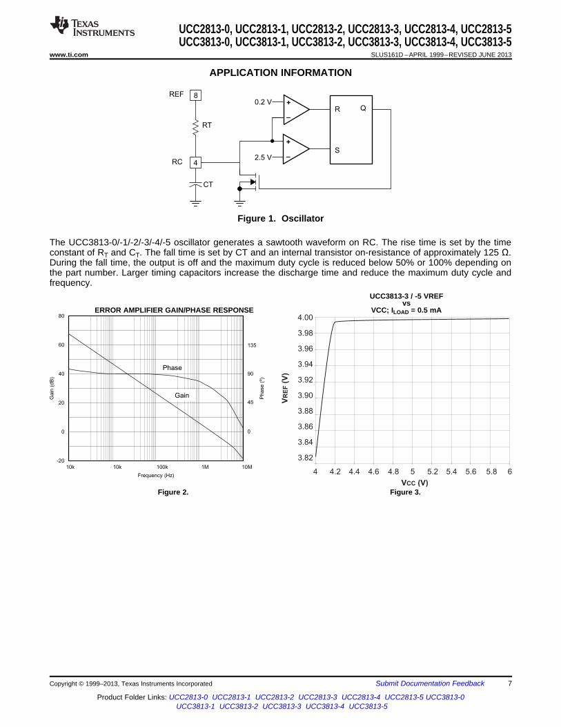
Figure 1. Oscillator
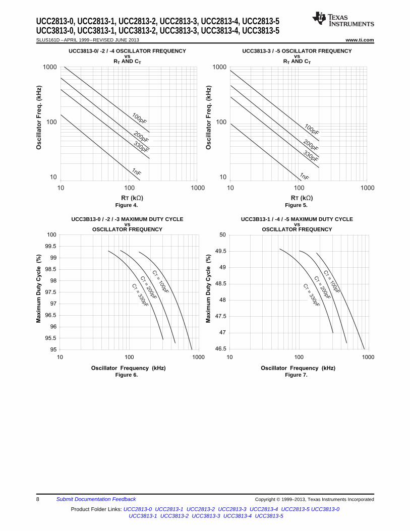
The UCC3813-0/-1/-2/-3/-4/-5 oscillator generates a sawtooth waveform on RC. The rise time is set by the timeconstant of RT and CT. The fall time is set by CT and an internal transistor on-resistance of approximately 125 Ω.During the fall time, the output is off and the maximum duty cycle is reduced below 50% or 100% depending onthe part number. Larger timing capacitors increase the discharge time and reduce the maximum duty cycle andfrequency.
UCC3813-3 / -5 VREFvs
ERROR AMPLIFIER GAIN/PHASE RESPONSE VCC; ILOAD = 0.5 mA
Figure 2. Figure 3.
Copyright © 1999–2013, Texas Instruments Incorporated Submit Documentation Feedback 7
Product Folder Links: UCC2813-0 UCC2813-1 UCC2813-2 UCC2813-3 UCC2813-4 UCC2813-5 UCC3813-0UCC3813-1 UCC3813-2 UCC3813-3 UCC3813-4 UCC3813-5
95
95.5
96
96.5
97
97.5
98
98.5
99
99.5
100
10 100 1000
Oscillator Frequency (kHz)
Ma
xim
um
Du
ty C
yc
le
(%)
C= 1
00pF
T
C= 2
00pF
T
C= 3
30pF
T
46.5
47
47.5
48
48.5
49
49.5
50
10 100 1000
Oscillator Frequency (kHz)
Ma
xim
um
Du
ty C
yc
le
(%)
C= 1
00pF
T
C= 2
00pF
T
C= 3
30pF
T
1000
100
10
10 100 1000
Oscilla
tor
Fre
q. (k
Hz)
R (k )T Ω
100pF
200pF330pF
1nF
1000
100
10
10 100 1000
Oscilla
tor
Fre
q. (k
Hz)
R (k )T Ω
100pF
200pF330pF
1nF
UCC2813-0, UCC2813-1, UCC2813-2, UCC2813-3, UCC2813-4, UCC2813-5UCC3813-0, UCC3813-1, UCC3813-2, UCC3813-3, UCC3813-4, UCC3813-5SLUS161D –APRIL 1999–REVISED JUNE 2013 www.ti.com
UCC3813-0/ -2 / -4 OSCILLATOR FREQUENCY UCC3813-3 / -5 OSCILLATOR FREQUENCYvs vs
RT AND CT RT AND CT
Figure 4. Figure 5.
UCC3B13-0 / -2 / -3 MAXIMUM DUTY CYCLE UCC3B13-1 / -4 / -5 MAXIMUM DUTY CYCLEvs vs
OSCILLATOR FREQUENCY OSCILLATOR FREQUENCY
Figure 6. Figure 7.
8 Submit Documentation Feedback Copyright © 1999–2013, Texas Instruments Incorporated
Product Folder Links: UCC2813-0 UCC2813-1 UCC2813-2 UCC2813-3 UCC2813-4 UCC2813-5 UCC3813-0UCC3813-1 UCC3813-2 UCC3813-3 UCC3813-4 UCC3813-5
0
0.6
0.7
0.8
0.9
1.0
1.1
-55-50 -25 0 25 50 75 100 125
Temperature (°C)
CO
MP
to C
S O
ffs
et
(Vo
lts
)
Slope = 1.8mV/ C°
0
50
100
150
200
250
300
350
400
450
500
100 200 300 400 500 600 700 800 900 1000
C (pF)T
Dead
Tim
e (
ns)
UCCx813/5
UCCx813/1/2/4
0
1
2
3
4
5
6
7
8
0 100 200 300 400 500 600 700 800 900 1000
Oscillator Frequency (kHz)
I(m
A)
CC
V= 10V, 1
nF
CC
V= 8V, 1
nF
CC
V = 10V, No Load
CC
V = 8V, No LoadCC
0
2
4
6
8
10
12
14
16
0 100 200 300 400 500 600 700 800 900 1000
Oscillator Frequency (kHz)
I(m
A)
CC
V= 10V, 1
nF
CC
V= 8V, 1
nF
CC
V = 10V, No Load
CC
V = 8V, No LoadCC
UCC2813-0, UCC2813-1, UCC2813-2, UCC2813-3, UCC2813-4, UCC2813-5UCC3813-0, UCC3813-1, UCC3813-2, UCC3813-3, UCC3813-4, UCC3813-5
www.ti.com SLUS161D –APRIL 1999–REVISED JUNE 2013
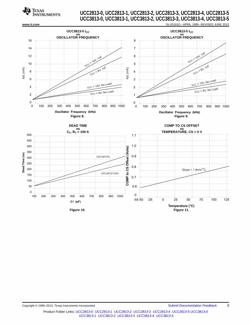
UCC3813-0 ICC UCC3813-5 ICCvs vs
OSCILLATOR FREQUENCY OSCILLATOR FREQUENCY
Figure 8. Figure 9.
DEAD TIME COMP TO CS OFFSETvs vs
CT, RT = 100 K TEMPERATURE, CS = 0 V
Figure 10. Figure 11.
Copyright © 1999–2013, Texas Instruments Incorporated Submit Documentation Feedback 9
Product Folder Links: UCC2813-0 UCC2813-1 UCC2813-2 UCC2813-3 UCC2813-4 UCC2813-5 UCC3813-0UCC3813-1 UCC3813-2 UCC3813-3 UCC3813-4 UCC3813-5
UCC2813-0, UCC2813-1, UCC2813-2, UCC2813-3, UCC2813-4, UCC2813-5UCC3813-0, UCC3813-1, UCC3813-2, UCC3813-3, UCC3813-4, UCC3813-5SLUS161D –APRIL 1999–REVISED JUNE 2013 www.ti.com
REVISION HISTORY
Changes from Revision B (April 2008) to Revision C Page
• Added Analog inputs RC and COMP in the ABSOLUTE MAXIMUM RATINGS Table ........................................................ 2• Added clarification to Analog Inputs min-max range in the ABSOLUTE MAXIMUM RATINGS table .................................. 2
Changes from Revision C (August 2010) to Revision D Page
• Added temperature range table note to second part of ordering information table for clarity in new datasheet format ...... 2• Added TI's general Absolute Maximum Ratings table note to end of ABSOLUTE MAXIMUM RATINGS table .................. 2• Added Thermal Information Table. ....................................................................................................................................... 2• Added UCCX813-3 to Total variation test condition line containing UCCx813-5 in ELECTRICAL
CHARACTERISTICS table ................................................................................................................................................... 3• Changed part numbers in Dead Time vs CT, RT = 100 k graph in APPLICATION INFORMATION .................................... 9• Changed layout from Unitrode Products datasheet to TI datasheet .................................................................................... 9
10 Submit Documentation Feedback Copyright © 1999–2013, Texas Instruments Incorporated
Product Folder Links: UCC2813-0 UCC2813-1 UCC2813-2 UCC2813-3 UCC2813-4 UCC2813-5 UCC3813-0UCC3813-1 UCC3813-2 UCC3813-3 UCC3813-4 UCC3813-5
PACKAGE OPTION ADDENDUM
www.ti.com 24-Aug-2014
Addendum-Page 1
PACKAGING INFORMATION
Orderable Device Status(1)
Package Type PackageDrawing
Pins PackageQty
Eco Plan(2)
Lead/Ball Finish(6)
MSL Peak Temp(3)
Op Temp (°C) Device Marking(4/5)
Samples
UCC2813D-0 ACTIVE SOIC D 8 75 Green (RoHS& no Sb/Br)
CU NIPDAU Level-1-260C-UNLIM -40 to 85 UCC2813D-02813D-0
UCC2813D-0G4 ACTIVE SOIC D 8 75 Green (RoHS& no Sb/Br)
CU NIPDAU Level-1-260C-UNLIM -40 to 85 UCC2813D-02813D-0
UCC2813D-1 ACTIVE SOIC D 8 75 Green (RoHS& no Sb/Br)
CU NIPDAU Level-1-260C-UNLIM -40 to 85 UCC2813D-12813D-1
UCC2813D-1G4 ACTIVE SOIC D 8 75 Green (RoHS& no Sb/Br)
CU NIPDAU Level-1-260C-UNLIM -40 to 85 UCC2813D-12813D-1
UCC2813D-2 ACTIVE SOIC D 8 75 Green (RoHS& no Sb/Br)
CU NIPDAU Level-1-260C-UNLIM -40 to 85 UCC2813D-22813D-2
UCC2813D-2G4 ACTIVE SOIC D 8 75 Green (RoHS& no Sb/Br)
CU NIPDAU Level-1-260C-UNLIM -40 to 85 UCC2813D-22813D-2
UCC2813D-3 ACTIVE SOIC D 8 75 Green (RoHS& no Sb/Br)
CU NIPDAU Level-1-260C-UNLIM -40 to 85 UCC2813D-32813D-3
UCC2813D-3G4 ACTIVE SOIC D 8 75 Green (RoHS& no Sb/Br)
CU NIPDAU Level-1-260C-UNLIM -40 to 85 UCC2813D-32813D-3
UCC2813D-4 ACTIVE SOIC D 8 75 Green (RoHS& no Sb/Br)
CU NIPDAU Level-1-260C-UNLIM -40 to 85 UCC2813D-42813D-4
UCC2813D-4G4 ACTIVE SOIC D 8 75 Green (RoHS& no Sb/Br)
CU NIPDAU Level-1-260C-UNLIM -40 to 85 UCC2813D-42813D-4
UCC2813D-5 ACTIVE SOIC D 8 75 Green (RoHS& no Sb/Br)
CU NIPDAU Level-1-260C-UNLIM -40 to 85 UCC2813D-52813D-5
UCC2813D-5G4 ACTIVE SOIC D 8 75 Green (RoHS& no Sb/Br)
CU NIPDAU Level-1-260C-UNLIM -40 to 85 UCC2813D-52813D-5
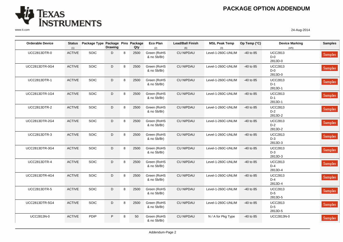
PACKAGE OPTION ADDENDUM
www.ti.com 24-Aug-2014
Addendum-Page 2
Orderable Device Status(1)
Package Type PackageDrawing
Pins PackageQty
Eco Plan(2)
Lead/Ball Finish(6)
MSL Peak Temp(3)
Op Temp (°C) Device Marking(4/5)
Samples
UCC2813DTR-0 ACTIVE SOIC D 8 2500 Green (RoHS& no Sb/Br)
CU NIPDAU Level-1-260C-UNLIM -40 to 85 UCC2813D-02813D-0
UCC2813DTR-0G4 ACTIVE SOIC D 8 2500 Green (RoHS& no Sb/Br)
CU NIPDAU Level-1-260C-UNLIM -40 to 85 UCC2813D-02813D-0
UCC2813DTR-1 ACTIVE SOIC D 8 2500 Green (RoHS& no Sb/Br)
CU NIPDAU Level-1-260C-UNLIM -40 to 85 UCC2813D-12813D-1
UCC2813DTR-1G4 ACTIVE SOIC D 8 2500 Green (RoHS& no Sb/Br)
CU NIPDAU Level-1-260C-UNLIM -40 to 85 UCC2813D-12813D-1
UCC2813DTR-2 ACTIVE SOIC D 8 2500 Green (RoHS& no Sb/Br)
CU NIPDAU Level-1-260C-UNLIM -40 to 85 UCC2813D-22813D-2
UCC2813DTR-2G4 ACTIVE SOIC D 8 2500 Green (RoHS& no Sb/Br)
CU NIPDAU Level-1-260C-UNLIM -40 to 85 UCC2813D-22813D-2
UCC2813DTR-3 ACTIVE SOIC D 8 2500 Green (RoHS& no Sb/Br)
CU NIPDAU Level-1-260C-UNLIM -40 to 85 UCC2813D-32813D-3
UCC2813DTR-3G4 ACTIVE SOIC D 8 2500 Green (RoHS& no Sb/Br)
CU NIPDAU Level-1-260C-UNLIM -40 to 85 UCC2813D-32813D-3
UCC2813DTR-4 ACTIVE SOIC D 8 2500 Green (RoHS& no Sb/Br)
CU NIPDAU Level-1-260C-UNLIM -40 to 85 UCC2813D-42813D-4
UCC2813DTR-4G4 ACTIVE SOIC D 8 2500 Green (RoHS& no Sb/Br)
CU NIPDAU Level-1-260C-UNLIM -40 to 85 UCC2813D-42813D-4
UCC2813DTR-5 ACTIVE SOIC D 8 2500 Green (RoHS& no Sb/Br)
CU NIPDAU Level-1-260C-UNLIM -40 to 85 UCC2813D-52813D-5
UCC2813DTR-5G4 ACTIVE SOIC D 8 2500 Green (RoHS& no Sb/Br)
CU NIPDAU Level-1-260C-UNLIM -40 to 85 UCC2813D-52813D-5
UCC2813N-0 ACTIVE PDIP P 8 50 Green (RoHS& no Sb/Br)
CU NIPDAU N / A for Pkg Type -40 to 85 UCC2813N-0
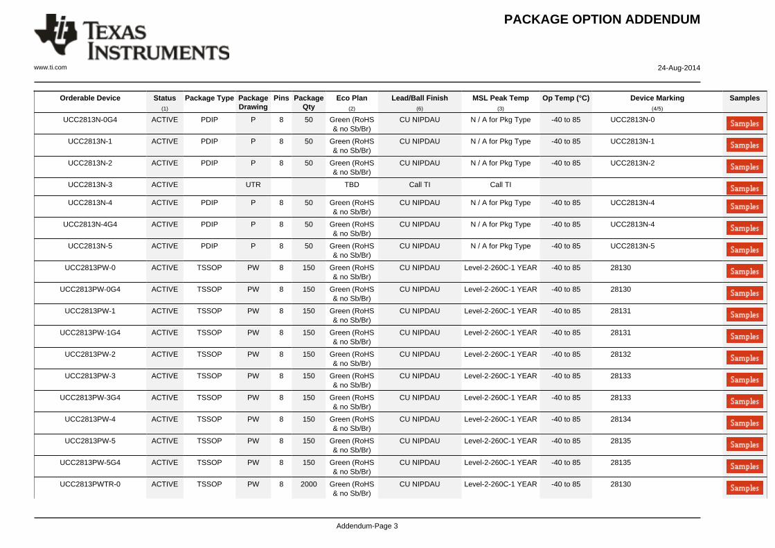
PACKAGE OPTION ADDENDUM
www.ti.com 24-Aug-2014
Addendum-Page 3
Orderable Device Status(1)
Package Type PackageDrawing
Pins PackageQty
Eco Plan(2)
Lead/Ball Finish(6)
MSL Peak Temp(3)
Op Temp (°C) Device Marking(4/5)
Samples
UCC2813N-0G4 ACTIVE PDIP P 8 50 Green (RoHS& no Sb/Br)
CU NIPDAU N / A for Pkg Type -40 to 85 UCC2813N-0
UCC2813N-1 ACTIVE PDIP P 8 50 Green (RoHS& no Sb/Br)
CU NIPDAU N / A for Pkg Type -40 to 85 UCC2813N-1
UCC2813N-2 ACTIVE PDIP P 8 50 Green (RoHS& no Sb/Br)
CU NIPDAU N / A for Pkg Type -40 to 85 UCC2813N-2
UCC2813N-3 ACTIVE UTR TBD Call TI Call TI
UCC2813N-4 ACTIVE PDIP P 8 50 Green (RoHS& no Sb/Br)
CU NIPDAU N / A for Pkg Type -40 to 85 UCC2813N-4
UCC2813N-4G4 ACTIVE PDIP P 8 50 Green (RoHS& no Sb/Br)
CU NIPDAU N / A for Pkg Type -40 to 85 UCC2813N-4
UCC2813N-5 ACTIVE PDIP P 8 50 Green (RoHS& no Sb/Br)
CU NIPDAU N / A for Pkg Type -40 to 85 UCC2813N-5
UCC2813PW-0 ACTIVE TSSOP PW 8 150 Green (RoHS& no Sb/Br)
CU NIPDAU Level-2-260C-1 YEAR -40 to 85 28130
UCC2813PW-0G4 ACTIVE TSSOP PW 8 150 Green (RoHS& no Sb/Br)
CU NIPDAU Level-2-260C-1 YEAR -40 to 85 28130
UCC2813PW-1 ACTIVE TSSOP PW 8 150 Green (RoHS& no Sb/Br)
CU NIPDAU Level-2-260C-1 YEAR -40 to 85 28131
UCC2813PW-1G4 ACTIVE TSSOP PW 8 150 Green (RoHS& no Sb/Br)
CU NIPDAU Level-2-260C-1 YEAR -40 to 85 28131
UCC2813PW-2 ACTIVE TSSOP PW 8 150 Green (RoHS& no Sb/Br)
CU NIPDAU Level-2-260C-1 YEAR -40 to 85 28132
UCC2813PW-3 ACTIVE TSSOP PW 8 150 Green (RoHS& no Sb/Br)
CU NIPDAU Level-2-260C-1 YEAR -40 to 85 28133
UCC2813PW-3G4 ACTIVE TSSOP PW 8 150 Green (RoHS& no Sb/Br)
CU NIPDAU Level-2-260C-1 YEAR -40 to 85 28133
UCC2813PW-4 ACTIVE TSSOP PW 8 150 Green (RoHS& no Sb/Br)
CU NIPDAU Level-2-260C-1 YEAR -40 to 85 28134
UCC2813PW-5 ACTIVE TSSOP PW 8 150 Green (RoHS& no Sb/Br)
CU NIPDAU Level-2-260C-1 YEAR -40 to 85 28135
UCC2813PW-5G4 ACTIVE TSSOP PW 8 150 Green (RoHS& no Sb/Br)
CU NIPDAU Level-2-260C-1 YEAR -40 to 85 28135
UCC2813PWTR-0 ACTIVE TSSOP PW 8 2000 Green (RoHS& no Sb/Br)
CU NIPDAU Level-2-260C-1 YEAR -40 to 85 28130
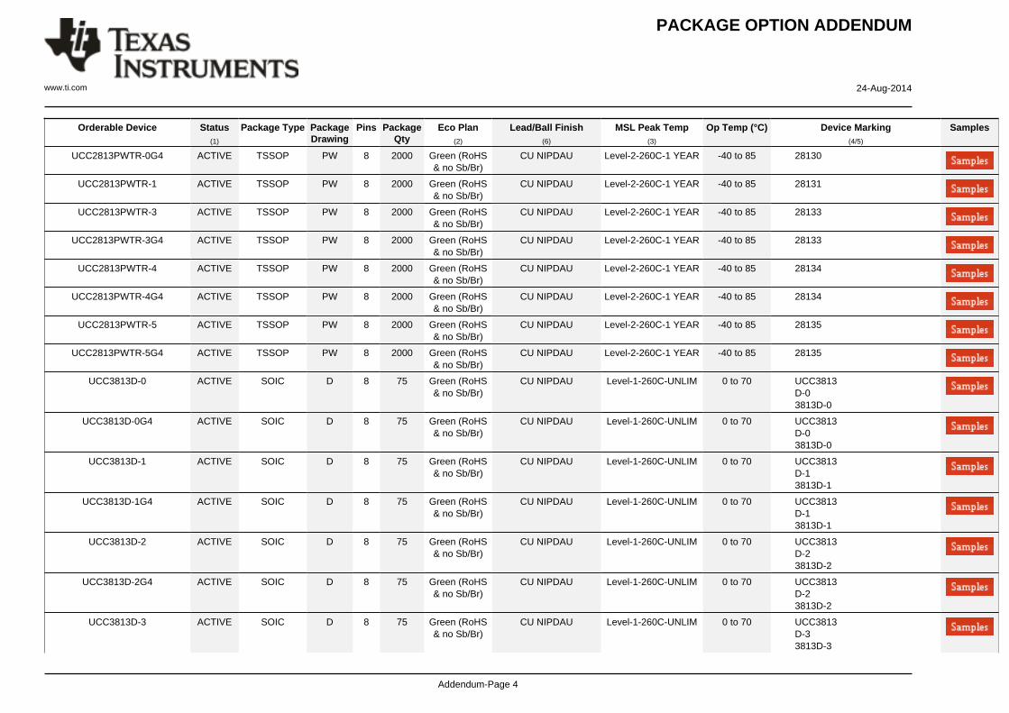
PACKAGE OPTION ADDENDUM
www.ti.com 24-Aug-2014
Addendum-Page 4
Orderable Device Status(1)
Package Type PackageDrawing
Pins PackageQty
Eco Plan(2)
Lead/Ball Finish(6)
MSL Peak Temp(3)
Op Temp (°C) Device Marking(4/5)
Samples
UCC2813PWTR-0G4 ACTIVE TSSOP PW 8 2000 Green (RoHS& no Sb/Br)
CU NIPDAU Level-2-260C-1 YEAR -40 to 85 28130
UCC2813PWTR-1 ACTIVE TSSOP PW 8 2000 Green (RoHS& no Sb/Br)
CU NIPDAU Level-2-260C-1 YEAR -40 to 85 28131
UCC2813PWTR-3 ACTIVE TSSOP PW 8 2000 Green (RoHS& no Sb/Br)
CU NIPDAU Level-2-260C-1 YEAR -40 to 85 28133
UCC2813PWTR-3G4 ACTIVE TSSOP PW 8 2000 Green (RoHS& no Sb/Br)
CU NIPDAU Level-2-260C-1 YEAR -40 to 85 28133
UCC2813PWTR-4 ACTIVE TSSOP PW 8 2000 Green (RoHS& no Sb/Br)
CU NIPDAU Level-2-260C-1 YEAR -40 to 85 28134
UCC2813PWTR-4G4 ACTIVE TSSOP PW 8 2000 Green (RoHS& no Sb/Br)
CU NIPDAU Level-2-260C-1 YEAR -40 to 85 28134
UCC2813PWTR-5 ACTIVE TSSOP PW 8 2000 Green (RoHS& no Sb/Br)
CU NIPDAU Level-2-260C-1 YEAR -40 to 85 28135
UCC2813PWTR-5G4 ACTIVE TSSOP PW 8 2000 Green (RoHS& no Sb/Br)
CU NIPDAU Level-2-260C-1 YEAR -40 to 85 28135
UCC3813D-0 ACTIVE SOIC D 8 75 Green (RoHS& no Sb/Br)
CU NIPDAU Level-1-260C-UNLIM 0 to 70 UCC3813D-03813D-0
UCC3813D-0G4 ACTIVE SOIC D 8 75 Green (RoHS& no Sb/Br)
CU NIPDAU Level-1-260C-UNLIM 0 to 70 UCC3813D-03813D-0
UCC3813D-1 ACTIVE SOIC D 8 75 Green (RoHS& no Sb/Br)
CU NIPDAU Level-1-260C-UNLIM 0 to 70 UCC3813D-13813D-1
UCC3813D-1G4 ACTIVE SOIC D 8 75 Green (RoHS& no Sb/Br)
CU NIPDAU Level-1-260C-UNLIM 0 to 70 UCC3813D-13813D-1
UCC3813D-2 ACTIVE SOIC D 8 75 Green (RoHS& no Sb/Br)
CU NIPDAU Level-1-260C-UNLIM 0 to 70 UCC3813D-23813D-2
UCC3813D-2G4 ACTIVE SOIC D 8 75 Green (RoHS& no Sb/Br)
CU NIPDAU Level-1-260C-UNLIM 0 to 70 UCC3813D-23813D-2
UCC3813D-3 ACTIVE SOIC D 8 75 Green (RoHS& no Sb/Br)
CU NIPDAU Level-1-260C-UNLIM 0 to 70 UCC3813D-33813D-3
PACKAGE OPTION ADDENDUM
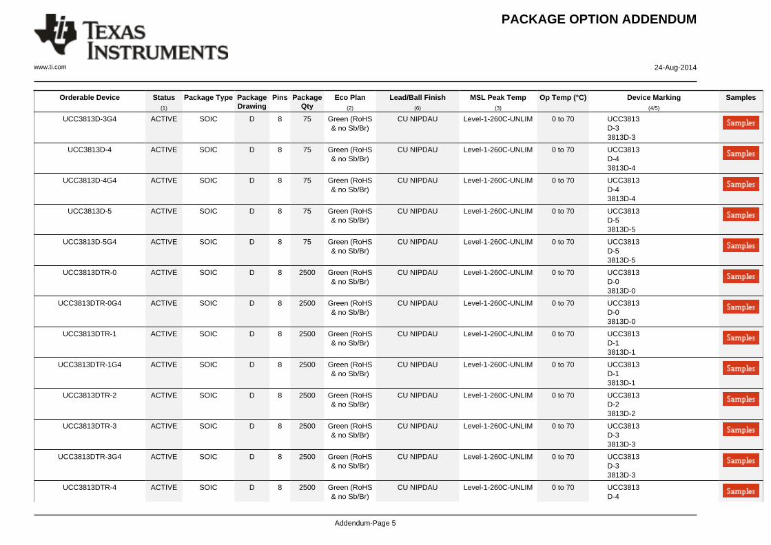
www.ti.com 24-Aug-2014
Addendum-Page 5
Orderable Device Status(1)
Package Type PackageDrawing
Pins PackageQty
Eco Plan(2)
Lead/Ball Finish(6)
MSL Peak Temp(3)
Op Temp (°C) Device Marking(4/5)
Samples
UCC3813D-3G4 ACTIVE SOIC D 8 75 Green (RoHS& no Sb/Br)
CU NIPDAU Level-1-260C-UNLIM 0 to 70 UCC3813D-33813D-3
UCC3813D-4 ACTIVE SOIC D 8 75 Green (RoHS& no Sb/Br)
CU NIPDAU Level-1-260C-UNLIM 0 to 70 UCC3813D-43813D-4
UCC3813D-4G4 ACTIVE SOIC D 8 75 Green (RoHS& no Sb/Br)
CU NIPDAU Level-1-260C-UNLIM 0 to 70 UCC3813D-43813D-4
UCC3813D-5 ACTIVE SOIC D 8 75 Green (RoHS& no Sb/Br)
CU NIPDAU Level-1-260C-UNLIM 0 to 70 UCC3813D-53813D-5
UCC3813D-5G4 ACTIVE SOIC D 8 75 Green (RoHS& no Sb/Br)
CU NIPDAU Level-1-260C-UNLIM 0 to 70 UCC3813D-53813D-5
UCC3813DTR-0 ACTIVE SOIC D 8 2500 Green (RoHS& no Sb/Br)
CU NIPDAU Level-1-260C-UNLIM 0 to 70 UCC3813D-03813D-0
UCC3813DTR-0G4 ACTIVE SOIC D 8 2500 Green (RoHS& no Sb/Br)
CU NIPDAU Level-1-260C-UNLIM 0 to 70 UCC3813D-03813D-0
UCC3813DTR-1 ACTIVE SOIC D 8 2500 Green (RoHS& no Sb/Br)
CU NIPDAU Level-1-260C-UNLIM 0 to 70 UCC3813D-13813D-1
UCC3813DTR-1G4 ACTIVE SOIC D 8 2500 Green (RoHS& no Sb/Br)
CU NIPDAU Level-1-260C-UNLIM 0 to 70 UCC3813D-13813D-1
UCC3813DTR-2 ACTIVE SOIC D 8 2500 Green (RoHS& no Sb/Br)
CU NIPDAU Level-1-260C-UNLIM 0 to 70 UCC3813D-23813D-2
UCC3813DTR-3 ACTIVE SOIC D 8 2500 Green (RoHS& no Sb/Br)
CU NIPDAU Level-1-260C-UNLIM 0 to 70 UCC3813D-33813D-3
UCC3813DTR-3G4 ACTIVE SOIC D 8 2500 Green (RoHS& no Sb/Br)
CU NIPDAU Level-1-260C-UNLIM 0 to 70 UCC3813D-33813D-3
UCC3813DTR-4 ACTIVE SOIC D 8 2500 Green (RoHS& no Sb/Br)
CU NIPDAU Level-1-260C-UNLIM 0 to 70 UCC3813D-4
PACKAGE OPTION ADDENDUM
www.ti.com 24-Aug-2014
Addendum-Page 6
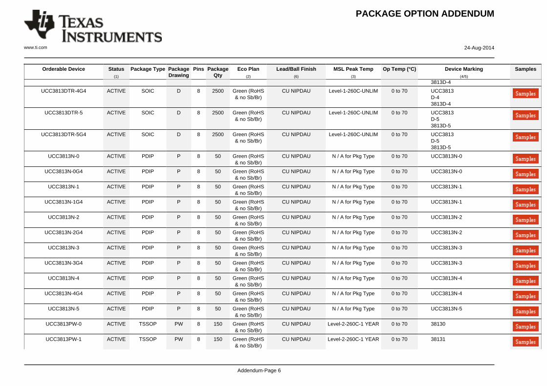
Orderable Device Status(1)
Package Type PackageDrawing
Pins PackageQty
Eco Plan(2)
Lead/Ball Finish(6)
MSL Peak Temp(3)
Op Temp (°C) Device Marking(4/5)
Samples
3813D-4
UCC3813DTR-4G4 ACTIVE SOIC D 8 2500 Green (RoHS& no Sb/Br)
CU NIPDAU Level-1-260C-UNLIM 0 to 70 UCC3813D-43813D-4
UCC3813DTR-5 ACTIVE SOIC D 8 2500 Green (RoHS& no Sb/Br)
CU NIPDAU Level-1-260C-UNLIM 0 to 70 UCC3813D-53813D-5
UCC3813DTR-5G4 ACTIVE SOIC D 8 2500 Green (RoHS& no Sb/Br)
CU NIPDAU Level-1-260C-UNLIM 0 to 70 UCC3813D-53813D-5
UCC3813N-0 ACTIVE PDIP P 8 50 Green (RoHS& no Sb/Br)
CU NIPDAU N / A for Pkg Type 0 to 70 UCC3813N-0
UCC3813N-0G4 ACTIVE PDIP P 8 50 Green (RoHS& no Sb/Br)
CU NIPDAU N / A for Pkg Type 0 to 70 UCC3813N-0
UCC3813N-1 ACTIVE PDIP P 8 50 Green (RoHS& no Sb/Br)
CU NIPDAU N / A for Pkg Type 0 to 70 UCC3813N-1
UCC3813N-1G4 ACTIVE PDIP P 8 50 Green (RoHS& no Sb/Br)
CU NIPDAU N / A for Pkg Type 0 to 70 UCC3813N-1
UCC3813N-2 ACTIVE PDIP P 8 50 Green (RoHS& no Sb/Br)
CU NIPDAU N / A for Pkg Type 0 to 70 UCC3813N-2
UCC3813N-2G4 ACTIVE PDIP P 8 50 Green (RoHS& no Sb/Br)
CU NIPDAU N / A for Pkg Type 0 to 70 UCC3813N-2
UCC3813N-3 ACTIVE PDIP P 8 50 Green (RoHS& no Sb/Br)
CU NIPDAU N / A for Pkg Type 0 to 70 UCC3813N-3
UCC3813N-3G4 ACTIVE PDIP P 8 50 Green (RoHS& no Sb/Br)
CU NIPDAU N / A for Pkg Type 0 to 70 UCC3813N-3
UCC3813N-4 ACTIVE PDIP P 8 50 Green (RoHS& no Sb/Br)
CU NIPDAU N / A for Pkg Type 0 to 70 UCC3813N-4
UCC3813N-4G4 ACTIVE PDIP P 8 50 Green (RoHS& no Sb/Br)
CU NIPDAU N / A for Pkg Type 0 to 70 UCC3813N-4
UCC3813N-5 ACTIVE PDIP P 8 50 Green (RoHS& no Sb/Br)
CU NIPDAU N / A for Pkg Type 0 to 70 UCC3813N-5
UCC3813PW-0 ACTIVE TSSOP PW 8 150 Green (RoHS& no Sb/Br)
CU NIPDAU Level-2-260C-1 YEAR 0 to 70 38130
UCC3813PW-1 ACTIVE TSSOP PW 8 150 Green (RoHS& no Sb/Br)
CU NIPDAU Level-2-260C-1 YEAR 0 to 70 38131
PACKAGE OPTION ADDENDUM
www.ti.com 24-Aug-2014
Addendum-Page 7
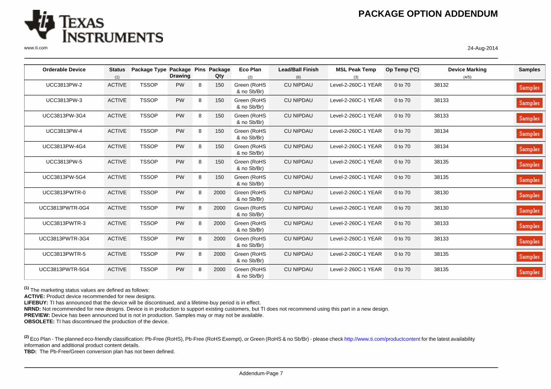
Orderable Device Status(1)
Package Type PackageDrawing
Pins PackageQty
Eco Plan(2)
Lead/Ball Finish(6)
MSL Peak Temp(3)
Op Temp (°C) Device Marking(4/5)
Samples
UCC3813PW-2 ACTIVE TSSOP PW 8 150 Green (RoHS& no Sb/Br)
CU NIPDAU Level-2-260C-1 YEAR 0 to 70 38132
UCC3813PW-3 ACTIVE TSSOP PW 8 150 Green (RoHS& no Sb/Br)
CU NIPDAU Level-2-260C-1 YEAR 0 to 70 38133
UCC3813PW-3G4 ACTIVE TSSOP PW 8 150 Green (RoHS& no Sb/Br)
CU NIPDAU Level-2-260C-1 YEAR 0 to 70 38133
UCC3813PW-4 ACTIVE TSSOP PW 8 150 Green (RoHS& no Sb/Br)
CU NIPDAU Level-2-260C-1 YEAR 0 to 70 38134
UCC3813PW-4G4 ACTIVE TSSOP PW 8 150 Green (RoHS& no Sb/Br)
CU NIPDAU Level-2-260C-1 YEAR 0 to 70 38134
UCC3813PW-5 ACTIVE TSSOP PW 8 150 Green (RoHS& no Sb/Br)
CU NIPDAU Level-2-260C-1 YEAR 0 to 70 38135
UCC3813PW-5G4 ACTIVE TSSOP PW 8 150 Green (RoHS& no Sb/Br)
CU NIPDAU Level-2-260C-1 YEAR 0 to 70 38135
UCC3813PWTR-0 ACTIVE TSSOP PW 8 2000 Green (RoHS& no Sb/Br)
CU NIPDAU Level-2-260C-1 YEAR 0 to 70 38130
UCC3813PWTR-0G4 ACTIVE TSSOP PW 8 2000 Green (RoHS& no Sb/Br)
CU NIPDAU Level-2-260C-1 YEAR 0 to 70 38130
UCC3813PWTR-3 ACTIVE TSSOP PW 8 2000 Green (RoHS& no Sb/Br)
CU NIPDAU Level-2-260C-1 YEAR 0 to 70 38133
UCC3813PWTR-3G4 ACTIVE TSSOP PW 8 2000 Green (RoHS& no Sb/Br)
CU NIPDAU Level-2-260C-1 YEAR 0 to 70 38133
UCC3813PWTR-5 ACTIVE TSSOP PW 8 2000 Green (RoHS& no Sb/Br)
CU NIPDAU Level-2-260C-1 YEAR 0 to 70 38135
UCC3813PWTR-5G4 ACTIVE TSSOP PW 8 2000 Green (RoHS& no Sb/Br)
CU NIPDAU Level-2-260C-1 YEAR 0 to 70 38135
(1) The marketing status values are defined as follows:ACTIVE: Product device recommended for new designs.LIFEBUY: TI has announced that the device will be discontinued, and a lifetime-buy period is in effect.NRND: Not recommended for new designs. Device is in production to support existing customers, but TI does not recommend using this part in a new design.PREVIEW: Device has been announced but is not in production. Samples may or may not be available.OBSOLETE: TI has discontinued the production of the device.
(2) Eco Plan - The planned eco-friendly classification: Pb-Free (RoHS), Pb-Free (RoHS Exempt), or Green (RoHS & no Sb/Br) - please check http://www.ti.com/productcontent for the latest availabilityinformation and additional product content details.TBD: The Pb-Free/Green conversion plan has not been defined.
PACKAGE OPTION ADDENDUM
www.ti.com 24-Aug-2014
Addendum-Page 8
Pb-Free (RoHS): TI's terms "Lead-Free" or "Pb-Free" mean semiconductor products that are compatible with the current RoHS requirements for all 6 substances, including the requirement thatlead not exceed 0.1% by weight in homogeneous materials. Where designed to be soldered at high temperatures, TI Pb-Free products are suitable for use in specified lead-free processes.Pb-Free (RoHS Exempt): This component has a RoHS exemption for either 1) lead-based flip-chip solder bumps used between the die and package, or 2) lead-based die adhesive used betweenthe die and leadframe. The component is otherwise considered Pb-Free (RoHS compatible) as defined above.Green (RoHS & no Sb/Br): TI defines "Green" to mean Pb-Free (RoHS compatible), and free of Bromine (Br) and Antimony (Sb) based flame retardants (Br or Sb do not exceed 0.1% by weightin homogeneous material)
(3) MSL, Peak Temp. - The Moisture Sensitivity Level rating according to the JEDEC industry standard classifications, and peak solder temperature.
(4) There may be additional marking, which relates to the logo, the lot trace code information, or the environmental category on the device.
(5) Multiple Device Markings will be inside parentheses. Only one Device Marking contained in parentheses and separated by a "~" will appear on a device. If a line is indented then it is a continuationof the previous line and the two combined represent the entire Device Marking for that device.
(6) Lead/Ball Finish - Orderable Devices may have multiple material finish options. Finish options are separated by a vertical ruled line. Lead/Ball Finish values may wrap to two lines if the finishvalue exceeds the maximum column width.
Important Information and Disclaimer:The information provided on this page represents TI's knowledge and belief as of the date that it is provided. TI bases its knowledge and belief on informationprovided by third parties, and makes no representation or warranty as to the accuracy of such information. Efforts are underway to better integrate information from third parties. TI has taken andcontinues to take reasonable steps to provide representative and accurate information but may not have conducted destructive testing or chemical analysis on incoming materials and chemicals.TI and TI suppliers consider certain information to be proprietary, and thus CAS numbers and other limited information may not be available for release.
In no event shall TI's liability arising out of such information exceed the total purchase price of the TI part(s) at issue in this document sold by TI to Customer on an annual basis.
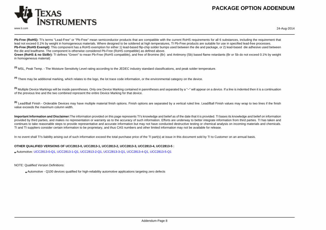
OTHER QUALIFIED VERSIONS OF UCC2813-0, UCC2813-1, UCC2813-2, UCC2813-3, UCC2813-4, UCC2813-5 :
• Automotive: UCC2813-0-Q1, UCC2813-1-Q1, UCC2813-2-Q1, UCC2813-3-Q1, UCC2813-4-Q1, UCC2813-5-Q1
NOTE: Qualified Version Definitions:
• Automotive - Q100 devices qualified for high-reliability automotive applications targeting zero defects
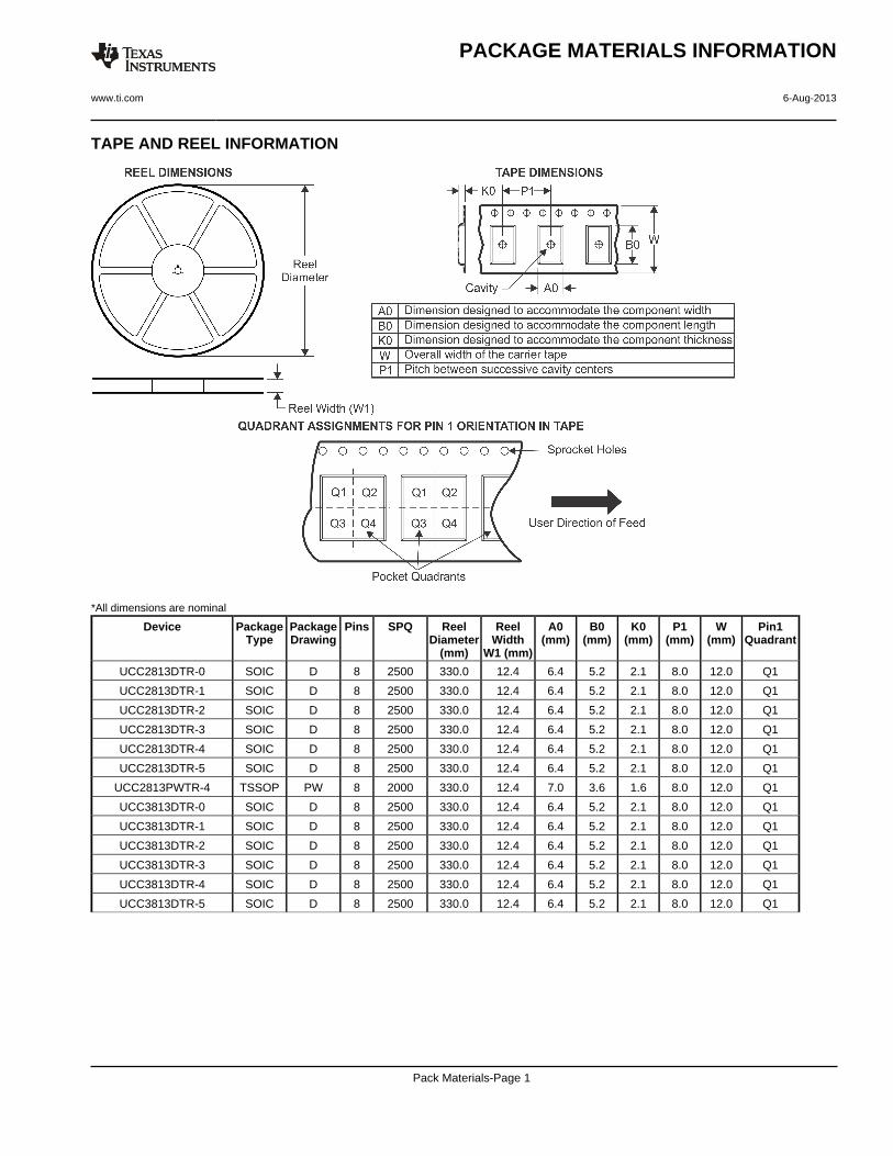
TAPE AND REEL INFORMATION
*All dimensions are nominal
Device PackageType
PackageDrawing
Pins SPQ ReelDiameter
(mm)
ReelWidth
W1 (mm)
A0(mm)
B0(mm)
K0(mm)
P1(mm)
W(mm)
Pin1Quadrant
UCC2813DTR-0 SOIC D 8 2500 330.0 12.4 6.4 5.2 2.1 8.0 12.0 Q1
UCC2813DTR-1 SOIC D 8 2500 330.0 12.4 6.4 5.2 2.1 8.0 12.0 Q1
UCC2813DTR-2 SOIC D 8 2500 330.0 12.4 6.4 5.2 2.1 8.0 12.0 Q1
UCC2813DTR-3 SOIC D 8 2500 330.0 12.4 6.4 5.2 2.1 8.0 12.0 Q1
UCC2813DTR-4 SOIC D 8 2500 330.0 12.4 6.4 5.2 2.1 8.0 12.0 Q1
UCC2813DTR-5 SOIC D 8 2500 330.0 12.4 6.4 5.2 2.1 8.0 12.0 Q1
UCC2813PWTR-4 TSSOP PW 8 2000 330.0 12.4 7.0 3.6 1.6 8.0 12.0 Q1
UCC3813DTR-0 SOIC D 8 2500 330.0 12.4 6.4 5.2 2.1 8.0 12.0 Q1
UCC3813DTR-1 SOIC D 8 2500 330.0 12.4 6.4 5.2 2.1 8.0 12.0 Q1
UCC3813DTR-2 SOIC D 8 2500 330.0 12.4 6.4 5.2 2.1 8.0 12.0 Q1
UCC3813DTR-3 SOIC D 8 2500 330.0 12.4 6.4 5.2 2.1 8.0 12.0 Q1
UCC3813DTR-4 SOIC D 8 2500 330.0 12.4 6.4 5.2 2.1 8.0 12.0 Q1
UCC3813DTR-5 SOIC D 8 2500 330.0 12.4 6.4 5.2 2.1 8.0 12.0 Q1
PACKAGE MATERIALS INFORMATION
www.ti.com 6-Aug-2013
Pack Materials-Page 1
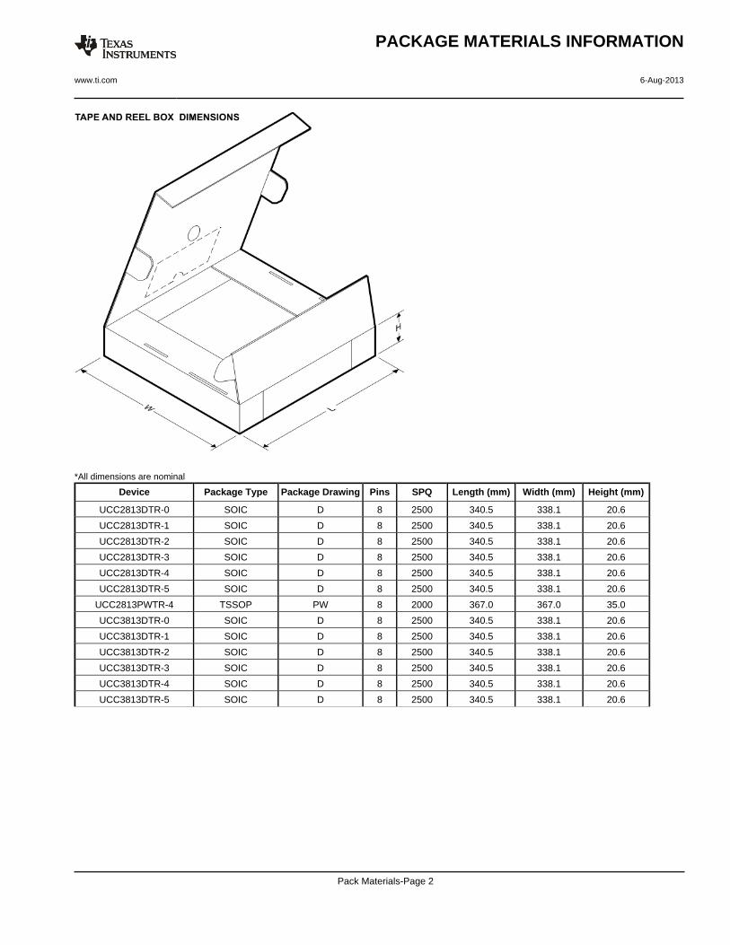
*All dimensions are nominal
Device Package Type Package Drawing Pins SPQ Length (mm) Width (mm) Height (mm)
UCC2813DTR-0 SOIC D 8 2500 340.5 338.1 20.6
UCC2813DTR-1 SOIC D 8 2500 340.5 338.1 20.6
UCC2813DTR-2 SOIC D 8 2500 340.5 338.1 20.6
UCC2813DTR-3 SOIC D 8 2500 340.5 338.1 20.6
UCC2813DTR-4 SOIC D 8 2500 340.5 338.1 20.6
UCC2813DTR-5 SOIC D 8 2500 340.5 338.1 20.6
UCC2813PWTR-4 TSSOP PW 8 2000 367.0 367.0 35.0
UCC3813DTR-0 SOIC D 8 2500 340.5 338.1 20.6
UCC3813DTR-1 SOIC D 8 2500 340.5 338.1 20.6
UCC3813DTR-2 SOIC D 8 2500 340.5 338.1 20.6
UCC3813DTR-3 SOIC D 8 2500 340.5 338.1 20.6
UCC3813DTR-4 SOIC D 8 2500 340.5 338.1 20.6
UCC3813DTR-5 SOIC D 8 2500 340.5 338.1 20.6
PACKAGE MATERIALS INFORMATION
www.ti.com 6-Aug-2013
Pack Materials-Page 2
IMPORTANT NOTICETexas Instruments Incorporated and its subsidiaries (TI) reserve the right to make corrections, enhancements, improvements and otherchanges to its semiconductor products and services per JESD46, latest issue, and to discontinue any product or service per JESD48, latestissue. Buyers should obtain the latest relevant information before placing orders and should verify that such information is current andcomplete. All semiconductor products (also referred to herein as “components”) are sold subject to TI’s terms and conditions of salesupplied at the time of order acknowledgment.TI warrants performance of its components to the specifications applicable at the time of sale, in accordance with the warranty in TI’s termsand conditions of sale of semiconductor products. Testing and other quality control techniques are used to the extent TI deems necessaryto support this warranty. Except where mandated by applicable law, testing of all parameters of each component is not necessarilyperformed.TI assumes no liability for applications assistance or the design of Buyers’ products. Buyers are responsible for their products andapplications using TI components. To minimize the risks associated with Buyers’ products and applications, Buyers should provideadequate design and operating safeguards.TI does not warrant or represent that any license, either express or implied, is granted under any patent right, copyright, mask work right, orother intellectual property right relating to any combination, machine, or process in which TI components or services are used. Informationpublished by TI regarding third-party products or services does not constitute a license to use such products or services or a warranty orendorsement thereof. Use of such information may require a license from a third party under the patents or other intellectual property of thethird party, or a license from TI under the patents or other intellectual property of TI.Reproduction of significant portions of TI information in TI data books or data sheets is permissible only if reproduction is without alterationand is accompanied by all associated warranties, conditions, limitations, and notices. TI is not responsible or liable for such altereddocumentation. Information of third parties may be subject to additional restrictions.Resale of TI components or services with statements different from or beyond the parameters stated by TI for that component or servicevoids all express and any implied warranties for the associated TI component or service and is an unfair and deceptive business practice.TI is not responsible or liable for any such statements.Buyer acknowledges and agrees that it is solely responsible for compliance with all legal, regulatory and safety-related requirementsconcerning its products, and any use of TI components in its applications, notwithstanding any applications-related information or supportthat may be provided by TI. Buyer represents and agrees that it has all the necessary expertise to create and implement safeguards whichanticipate dangerous consequences of failures, monitor failures and their consequences, lessen the likelihood of failures that might causeharm and take appropriate remedial actions. Buyer will fully indemnify TI and its representatives against any damages arising out of the useof any TI components in safety-critical applications.In some cases, TI components may be promoted specifically to facilitate safety-related applications. With such components, TI’s goal is tohelp enable customers to design and create their own end-product solutions that meet applicable functional safety standards andrequirements. Nonetheless, such components are subject to these terms.No TI components are authorized for use in FDA Class III (or similar life-critical medical equipment) unless authorized officers of the partieshave executed a special agreement specifically governing such use.Only those TI components which TI has specifically designated as military grade or “enhanced plastic” are designed and intended for use inmilitary/aerospace applications or environments. Buyer acknowledges and agrees that any military or aerospace use of TI componentswhich have not been so designated is solely at the Buyer's risk, and that Buyer is solely responsible for compliance with all legal andregulatory requirements in connection with such use.TI has specifically designated certain components as meeting ISO/TS16949 requirements, mainly for automotive use. In any case of use ofnon-designated products, TI will not be responsible for any failure to meet ISO/TS16949.Products ApplicationsAudio www.ti.com/audio Automotive and Transportation www.ti.com/automotiveAmplifiers amplifier.ti.com Communications and Telecom www.ti.com/communicationsData Converters dataconverter.ti.com Computers and Peripherals www.ti.com/computersDLP® Products www.dlp.com Consumer Electronics www.ti.com/consumer-appsDSP dsp.ti.com Energy and Lighting www.ti.com/energyClocks and Timers www.ti.com/clocks Industrial www.ti.com/industrialInterface interface.ti.com Medical www.ti.com/medicalLogic logic.ti.com Security www.ti.com/securityPower Mgmt power.ti.com Space, Avionics and Defense www.ti.com/space-avionics-defenseMicrocontrollers microcontroller.ti.com Video and Imaging www.ti.com/videoRFID www.ti-rfid.comOMAP Applications Processors www.ti.com/omap TI E2E Community e2e.ti.comWireless Connectivity www.ti.com/wirelessconnectivity
Mailing Address: Texas Instruments, Post Office Box 655303, Dallas, Texas 75265Copyright © 2014, Texas Instruments Incorporated