Embed Size (px)
Citation preview

SLOC™ TW3801-C1, TW3811- C1 Design Guide
AN1804 Rev. 0.00 Page 1 of 26
November 27, 2012
AN1804
Rev. 0.00
November 27, 2012
APPLICATION NOTE
SLOC™ TW3801-C1, TW3811- C1 Design Guide

SLOC™ TW3801-C1, TW3811- C1 Design Guide
AN1804 Rev. 0.00 Page 2 of 26
November 27, 2012
Table of Contents Introduction ..................................................................................................................................................................................... 3
SLOC System Operation ................................................................................................................................................................. 3
Hardware Design Guide .................................................................................................................................................................. 4
SLOC Operating Mode Selection ................................................................................................................................................ 4
Ethernet PHY Interface Mode ........................................................................................................................................ 4
SOC(MAC) Interface Mode.............................................................................................................................................. 4
SLOC Pass-Through Mode .............................................................................................................................................. 5
SLOC Downlink/Uplink Throughput Settings ........................................................................................................................... 7
Data Rate Vs Cable Length ......................................................................................................................................................... 8
Mode Selection by Pin Strap ...................................................................................................................................................... 9
COAX Pin Application ................................................................................................................................................................. 10
TW3811 CVBS Output Circuit ................................................................................................................................................... 11
Ethernet PHY Interfacing ........................................................................................................................................................... 12
MII Interface with Ethernet PHY .................................................................................................................................. 12
RMII Interface with Ethernet PHY ............................................................................................................................... 13
PHY Address Settings ................................................................................................................................................... 15
Ethernet PHY Reset Application .................................................................................................................................. 15
SOC (CODEC) Chip Interfaces ................................................................................................................................................... 16
MII Interface with SOC .................................................................................................................................................. 16
RMII Interface with SOC ............................................................................................................................................... 16
ESD/EMI Solution ....................................................................................................................................................................... 17
SLOC Firmware .............................................................................................................................................................................. 18
SLOC Performance Check ............................................................................................................................................................ 20
PER (Packet Error Rate) Measurement .................................................................................................................................. 20
Downlink PER ................................................................................................................................................................. 20
Uplink PER ...................................................................................................................................................................... 20
SLOC Signals Evaluation ........................................................................................................................................................... 20
PCB Layout Guide .......................................................................................................................................................................... 21
COAX_OUT and COAX_IN ........................................................................................................................................................... 21
LOAD_DRV (Pin 66) .................................................................................................................................................................... 22
CVBS Input for TW3801 ............................................................................................................................................................ 22
CVBS Output for TW3811 ......................................................................................................................................................... 22
Power Distribution ...................................................................................................................................................................... 23
Decoupling Capacitors for Power Pins .................................................................................................................................... 24
Ground Considerations .............................................................................................................................................................. 24
Multi-Channel Design ................................................................................................................................................................. 25

SLOC™ TW3801-C1, TW3811- C1 Design Guide
AN1804 Rev. 0.00 Page 3 of 26
November 27, 2012
Introduction This application note provides TW3801/TW3811 hardware design and PCB layout guide. It also includes SLOC link flow
control (state machine). For ESD and EMI solution, the guidelines to select the components are provided.
SLOC System Operation A SLOC system is a pair of TW3801 and TW3811 chips connected via COAX cable. The TW3801 (the “SLOC™
transmitter”) is placed at the IP camera end, and the TW3811 (the “SLOC™ receiver”) is placed at the NVR/DVR end. The
downlink IP packets (typically compressed video data) from the camera are modulated and transmitted “downstream”
with the CVBS signal over the COAX connection. The uplink IP packets (PTZ control signals, etc.) from the NVR are
modulated and transmitted “upstream” through the COAX cable.
The SLOC signals are composed of base-band composite video and modulated downlink and uplink signals. These
signals covered a 42MHz bandwidth as shown in Figure 1.
Since SLOC is intended to operate with conventional 75Ω COAX cable, the COAX input and output impedances should be
matched to the cable impedance to minimize reflection. The COAX_O pin uses a current-mode driver circuit (high
impedance output), and therefore requires a 75Ω resistor to ground to generate the final signal with a 75Ω source
impedance. The COAX_I/O and overall SLOC system configuration are shown in Figure 2.
8MHz 2.5MHz
Base-band CVBS Downlink Uplink
f (MHz)
5.4MHz 14.75MHz 22.75MHz 37.75MHz 40.25MHz
FIGURE 1. SLOC SIGNAL SPECTRUM
TW3811
470µF/10V
75R0
0.1µF
10µF
COAX_I
COAX_O
CVBS_O
MII/RMII
COAX cable
0.1µF
TW3801
COAX_I
COAX_O
CVBS_I
MII/RMII
10µF
75R0
470µF/10V
FIGURE 2. SLOC COAX I/O CONFIGURATION

SLOC™ TW3801-C1, TW3811- C1 Design Guide
AN1804 Rev. 0.00 Page 4 of 26
November 27, 2012
Hardware Design Guide
SLOC Operating Mode Selection
The SLOC chips can be embedded in an IP Camera/NVR system or used to create “dongle” adapters. Depending on the
system requirements, the SLOC chip can operate in one of three different modes. The first is the Ethernet PHY interface
mode, which is most often used in a SLOC dongle application. The second is the SOC (System-On-a-Chip, also called MAC)
interface mode, for SLOC-embedded systems. The third is a pass-through mode that directs MII data from the SOC to
flow directly through the SLOC IC and into an Ethernet PHY. This mode allows the camera to operate as a traditional IP
camera when not connected to a SLOC receiver.
ETHERNET PHY INTERFACE MODE
The TW38x1 MIIA pins are designed to connect to a Fast Ethernet PHY or Switch (PHY Mode). The MII Tx/Rx clocks are
generated by the PHY chip, and connect to the TW38x1’s TX_CLK/RX_CLK input pins. This mode can be selected by tying
TW38x1 pin 93 (MODE_S3) to ground or by setting register 0x01 bits[4:3] = 00 with register 0x01 bit[0] = 1. A 1.5kΩ
pull-up resistor on MDIO is required in this mode to support the Ethernet PHY link status check. The application diagram
is shown in Figure 3.
SOC(MAC) INTERFACE MODE
This mode is used for SLOC embedded systems. The MIIB pins interface with SOC (System-On-a-Chip, for example a
codec) chips. This mode can be selected by tying pin number 93 (MODE_S3) to 3.3V with a 10kΩ pull-up resistor or by
setting register 0x01 bit[4:3] = 01 with register 0x01 bit[0] = 1. The application diagram is shown in Figure 4.
RJ45 IP CAM
Or
NVR
TW38x1
MIIA
MODE_S3
SLOC COAX I/O Fast
Ether
PHY
FIGURE 3. ETHERNET PHY INTERFACE MODE FOR DONGLE SOLUTION
MIIB
TW38x1
SOC
(MAC)
SLOC COAX I/O
MODE_S3
3.3V
FIGURE 4. SOC INTERFACE MODE FOR EMBEDDED SYSTEM

SLOC™ TW3801-C1, TW3811- C1 Design Guide
AN1804 Rev. 0.00 Page 5 of 26
November 27, 2012
If the SOC (Codec) chip doesn’t provide a TX_ER (Transmit Error) signal, just leave the TX_ER_B (Pin# 26) pin
unconnected. Since the MDC and MDIO management signals are not used in this mode, they should be tied to 3.3V with
10kΩ pull-up resistors.
SLOC PASS-THROUGH MODE
Even with a TW3801 SLOC transmitter chip embedded into an IP camera, the camera can still provide a legacy RJ45
Ethernet interface with a minimum of additional components. In this mode, the SLOC IP modulation/demodulation
processes are disabled, and the MII signals are passed between the MIIA and MIIB interfaces. The block diagram of a
SLOC-embedded IP camera with this RJ45 pass-through mode is shown in Figure 5.
The MII connections for pass-through mode are shown in Figure 6.
TW3801 MDC 3 MDIO 4
RX_DV_A 5 RX_ER_A 6
RX_D0_A 7 RX_D1_A 10 RX_D2_A 11 RX_D3_A 12
TX_EN_A 14 TX_ER_A 17
TX_D0_A 18 TX_D1_A 19 TX_D2_A 20 TX_D3_A 21
RX_CLK_A 22 TX_CLK_A 25
TX_ER_B 26 TX_EN_B 29 TX_D0_B 30 TX_D1_B 31 TX_D2_B 32 TX_D3_B 33
RX_CLK_B 36 TX_CLK_B 37
RX_ER_B 38 RX_DV_B 39 RX_D0_B 40 RX_D1_B 41 RX_D2_B 44 RX_D3_B 45
330Ω
LED_0 53
SOC (CODEC)
TX_ER TX_EN
TXD0 TXD1 TXD2 TXD3
RX_CLK TX_CLK
RX_ER RX_DV
RXD0 RXD1 RXD2 RXD3
MDC MDIO
Ethernet PHY or
RXDV RXD0 RXD1 RXD2 RXD3
RXC TXC
TXD0 TXD2 TXD3
TXEN
MDC MDIO
CRS COL
RXER
TXD1
Switch (PHY Mode)
Transmit Data 2 Transmit Data 1 Transmit Data 0 Transmit Enable
Receiver Data 2 Receiver Data 1 Receiver Data 0 Receiver Data Valid Receiver Error Receiver Clock Transmit Clock Transmit Data 3
Receiver Data 3
MDIO
10kΩ
MDC
10kΩ
3_3VD
MDC MDIO
1.5kΩ
3_3V
LED
NOTE: 1. LED_0 : MII mode selection 2. Set register 0x01[4:3] = 10 and register 0x01[0] = 1
FIGURE 5. SLOC EMBEDDED IP CAMERA DESIGN BLOCK
SLOC I/O
to NVR side
with
TW3811
CAT5 NVR
Fast
Ether
PHY
ISP/SOC
(MAC)
TW3801
MIIA
MIIB
FIGURE 6. SLOC PASS-THROUGH MODE WITH MII INTERFACE
3_3VD

SLOC™ TW3801-C1, TW3811- C1 Design Guide
AN1804 Rev. 0.00 Page 6 of 26
November 27, 2012
The RMII connections for pass-through mode are shown in Figure 7.
TW3801
MDC 3 MDIO 4
RX_DV_A 5 RX_D0_A 7 RX_D1_A 10
TX_EN_A 14 TX_D0_A 18 TX_D1_A 19
TX_CLK_A 25
TX_EN_B 29 TX_D0_B 30 TX_D1_B 31
RX_ER_B 38 RX_DV_B 39 RX_D0_B 40 RX_D1_B 41
RX_ER_A 6
LED_0 53
SOC (CODEC) TX_EN
TXD0 TXD1
TX_CLK
RX_ER RX_DV
RXD0 RXD1
MDC MDIO
Ethernet PHY or
CRS_DV RXD0 RXD1 TXC
TXD0 TXEN
MDC MDIO
RXER TXD1
Switch (PHY Mode)
10kΩ 10kΩ
3_3VD
2N3906 3
2 1
3_3V
10kΩ
LED
4.7kΩ
330Ω
MDC MDIO
Transmit Data 1 Transmit Data 0 Transmit Enable
50MHz Reference clock Receive Data 1 Receive Data 0 Receive Data Valid Receive Error
1.5kΩ
MDC MDIO
3_3VD
NOTE: 1. LED_0 : RMII mode selection 2. Set register 0x01[4:3] = 10 and register 0x01[0] = 1. 3. Set register 0x01[6] = 0 for 50MHz reference clock output from pin #50
FIGURE 7. SLOC PASS-THROUGH MODE WITH RMII INTERFACE

SLOC™ TW3801-C1, TW3811- C1 Design Guide
AN1804 Rev. 0.00 Page 7 of 26
November 27, 2012
SLOC Downlink/Uplink Throughput Settings
SLOC link transmission speed can be selected by the logic level of the MODE_S0 and MODE_S1 external pins, or by
register 0x0A. When register 0x01[0] = 0, link speed is determined by the pins. When register 0x01[0] = 1, link speed is
determined by register0x0A. By default (since the default setting of register 0x01[0] is 0), the speed after a reset or
power-on is determined by the external pins. The available speeds and settings are shown in Table 1. The speed setting
for the TW3801 determines downlink throughput and the setting for the TW3811 defines uplink throughput. The
recommended settings (in bold) are 36Mbps downstream (for maximum video throughput), and 4Mbps upstream (since
there is very little upstream data, lowering the maximum rate from 11Mbps has no performance impact on an IP
camera, while the lower 4Mbps rate enables slightly longer cable lengths than 11Mbps).
TABLE 1. SLOC LINK DATA RATE SETTINGS
TW3801 (DOWNLINK THROUGHPUT) TW3811 (UPLINK THROUGHPUT)
SPEED REGISTER 0X0A EXTERNAL PINS SPEED REGISTER 0X0A EXTERNAL PINS
36Mbps 0x13 MODE_S0 = 0
MODE_S1 = 0 11Mbps 0x13
MODE_S0 = 0
MODE_S1 = 0
32Mbps 0x12 - 10Mbps 0x12 -
28Mbps 0x11 MODE_S0 = 1
MODE_S1 = 0 9Mbps 0x11
MODE_S0 = 1
MODE_S1 = 0
25Mbps 0x0C MODE_S0 = 0
MODE_S1 = 1 7.5Mbps 0x0C -
23Mbps 0x0B - 7Mbps 0x0B -
21Mbps 0x0A MODE_S0 = 1
MODE_S1 = 1 6.5Mbps 0x0A -
19Mbps 0x09 - 6Mbps 0x09 -
14Mbps 0x08 - 4.5Mbps 0x08 -
12Mbps 0x04 - 4Mbps 0x04 MODE_S0 = 0
MODE_S1 = 1
11Mbps 0x03 - 3.5Mbps 0x03 -
10Mbps 0x02 - 3Mbps 0x02 MODE_S0 = 1
MODE_S1 = 1
9Mbps 0x01 - 2.5Mbps 0x01 -
7Mbps 0x00 - 2Mbps 0x00 -
NOTE: Register 0x0A settings are valid and override external pin values when register 0x01[0] = 1.

SLOC™ TW3801-C1, TW3811- C1 Design Guide
AN1804 Rev. 0.00 Page 8 of 26
November 27, 2012
Data Rate Vs Cable Length
Since SLOC™ transmits at higher frequencies than analog video; the maximum cable length is a function of the cable
quality and composition. The following tables show examples of cable distance vs. downstream and upstream data rates
for copper-core RG59 and the less-expensive SYV75-3 (64) cable. The SLOC compliance test measures upstream data
rate at 4Mbps, while downstream data rate is 36Mbps for 500m RG59 Belden #543945 cable.
VENDOR STYLE
CONDUCTOR
NO./MM
DIAMETER IN
INSULATION (mm)
OUTER
CONDUCTOR
BRAIDING
STANDARD
COMPLIANCE
Shenzhen
Shuangying Cable Co. SYV75-3 (3C-2V) Bare Copper 1/0.5 3 64 GB/T14864-93
Length in Meters
0 150 300 450 600 750
3Mbps4Mbps9Mbps
21Mbps 11Mbps
3Mbps4Mbps9Mbps
25Mbps 11Mbps
3Mbps4Mbps9Mbps
28Mbps 11Mbps
3Mbps4Mbps9Mbps
36Mbps 11Mbps
Downstream Upstream
Data Rate Data RateRG59 Belden #543945
0 100 200 300 400 500
3Mbps 4Mbps 9Mbps
21Mbps 11Mbps
3Mbps 4Mbps 9Mbps
25Mbps 11Mbps
3Mbps 4Mbps 9Mbps
28Mbps 11Mbps
3Mbps 4Mbps 9Mbps
36Mbps 11Mbps
Length in Meters
SYV75 - 3 (64) Downstream Upstream Data Rate Data Rate
SLOC™ TW3801-C1, TW3811- C1 Design Guide
AN1804 Rev. 0.00 Page 9 of 26
November 27, 2012
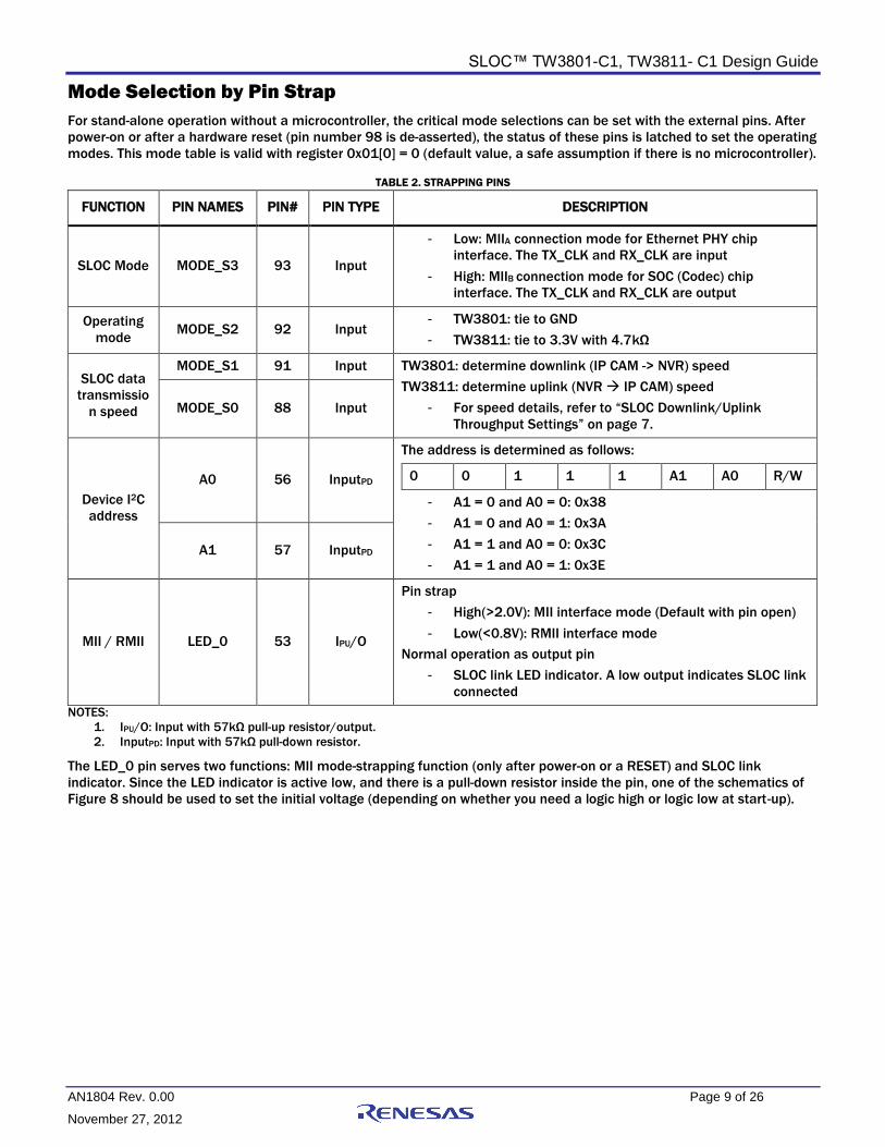
Mode Selection by Pin Strap
For stand-alone operation without a microcontroller, the critical mode selections can be set with the external pins. After
power-on or after a hardware reset (pin number 98 is de-asserted), the status of these pins is latched to set the operating
modes. This mode table is valid with register 0x01[0] = 0 (default value, a safe assumption if there is no microcontroller).
TABLE 2. STRAPPING PINS
FUNCTION PIN NAMES PIN# PIN TYPE DESCRIPTION
SLOC Mode MODE_S3 93 Input
- Low: MIIA connection mode for Ethernet PHY chip
interface. The TX_CLK and RX_CLK are input
- High: MIIB connection mode for SOC (Codec) chip
interface. The TX_CLK and RX_CLK are output
Operating
mode MODE_S2 92 Input
- TW3801: tie to GND
- TW3811: tie to 3.3V with 4.7kΩ
SLOC data
transmissio
n speed
MODE_S1 91 Input TW3801: determine downlink (IP CAM -> NVR) speed
TW3811: determine uplink (NVR IP CAM) speed
- For speed details, refer to “SLOC Downlink/Uplink
Throughput Settings” on page 7.
MODE_S0 88 Input
Device I2C
address
A0 56 InputPD
The address is determined as follows:
0 0 1 1 1 A1 A0 R/W
- A1 = 0 and A0 = 0: 0x38
- A1 = 0 and A0 = 1: 0x3A
- A1 = 1 and A0 = 0: 0x3C
- A1 = 1 and A0 = 1: 0x3E A1 57 InputPD
MII / RMII LED_0 53 IPU/O
Pin strap
- High(>2.0V): MII interface mode (Default with pin open)
- Low(<0.8V): RMII interface mode
Normal operation as output pin
- SLOC link LED indicator. A low output indicates SLOC link
connected
NOTES:
1. IPU/O: Input with 57kΩ pull-up resistor/output.
2. InputPD: Input with 57kΩ pull-down resistor.
The LED_0 pin serves two functions: MII mode-strapping function (only after power-on or a RESET) and SLOC link
indicator. Since the LED indicator is active low, and there is a pull-down resistor inside the pin, one of the schematics of
Figure 8 should be used to set the initial voltage (depending on whether you need a logic high or logic low at start-up).

SLOC™ TW3801-C1, TW3811- C1 Design Guide
AN1804 Rev. 0.00 Page 10 of 26
November 27, 2012
FIGURE 8. LED_0 PIN APPLICATION
COAX Pin Application
For both the TW3801 and the TW3811, the SLOC signal is transmitted through the COAX_O pin and received through
COAX_I.
FIGURE 9. SLOC COAX I/O CIRCUIT
Since the SLOC signal includes base-band CVBS and must drive 75Ω, a 470µF AC-coupling capacitor is required to pass
frequencies down to 50Hz (PAL vertical sync) and prevent a sagging. However, large-value electrolytics do not have very
good high-frequency performance, so a 100nF is placed in parallel to accurately pass the 12MHz to 42MHz IP signal.
Adding the 150nH inductor is recommended for better return loss performance. In the receive path, a 10µF AC-coupling
capacitor adequately passes both the video and IP frequencies into the higher-impedance COAX_I pin.
COAX_OUT
L32 150nH
C8 100nF
+
C9 470µF/16V
SLOC IN/OUT
CON2 BNC
1
2 3
4 5
R14 75Ω
DRLOAD
TW38x1C1
LOAD_DRV 66 COAX_O 67
COAX_I
78
COAX_IN
R13 75Ω
C3 10µF
D1 ESD
MII mode (pin high at reset)
RMII mode

SLOC™ TW3801-C1, TW3811- C1 Design Guide
AN1804 Rev. 0.00 Page 11 of 26
November 27, 2012
TW3811 CVBS Output Circuit
To drive the CVBS signal onto a 75Ω cable, the video amplitude should be 2VP-P with a 75Ω series source terminating
resistor. Since the signal from the TW3811 is inverted and ≈0.83 VP-P, an inverting amplifier with x2.4 gain is required.
The low-cost solution with clamping circuit is shown in Figure 10. With this circuit, brief brightness changes may be seen
for mostly-black to mostly-white (and vice-versa) scene transitions.
FIGURE 10. LOW-COST CVBS OUTPUT CIRCUIT
The best solution is to use a video driver with integrated DC-restore, as shown in Figure 11.
AVD_A
C5 47µF/10V
TW3811-C1
CVBS_OUT 68
D7 BAT54HT1G
AVD_A
C31 100nF
R3 10kΩ
R4 4.7kΩ
R5 1.5kΩ
R6 24kΩ
+
-
U13 EL8101 SOT23-5
3
4 1
5
2
C7 4.7µF
+
C10 470µF /16V
CON1
1
2 3
4 5
AVD_A
R10 DNP
R1 75Ω
R7 DNP R8
100Ω
FIGURE 11. BETTER CVBS OUTPUT CIRCUIT
C51 47µF C1206
U10 ISL59110
GND 2
VS+ 6
IN+ 1
EN 5
OUT 4
SAG 3
AVD_A
C55 0.1uF
C57 0.1µF
C5 47µF/10V
TW3811-C1
CVBS_OUT 68
C31 0.1µF
R3 10kΩ
R4 10kΩ
R5 10kΩ
R6 12kΩ
+
-
U13 EL8101 SOT23-5
3
4 1
5
2
C7 0.1µF
AVD_A
AVD_A CON1
1
2 3
4 5
R13 75Ω
C52 100µF C1206
SLOC™ TW3801-C1, TW3811- C1 Design Guide
AN1804 Rev. 0.00 Page 12 of 26
November 27, 2012
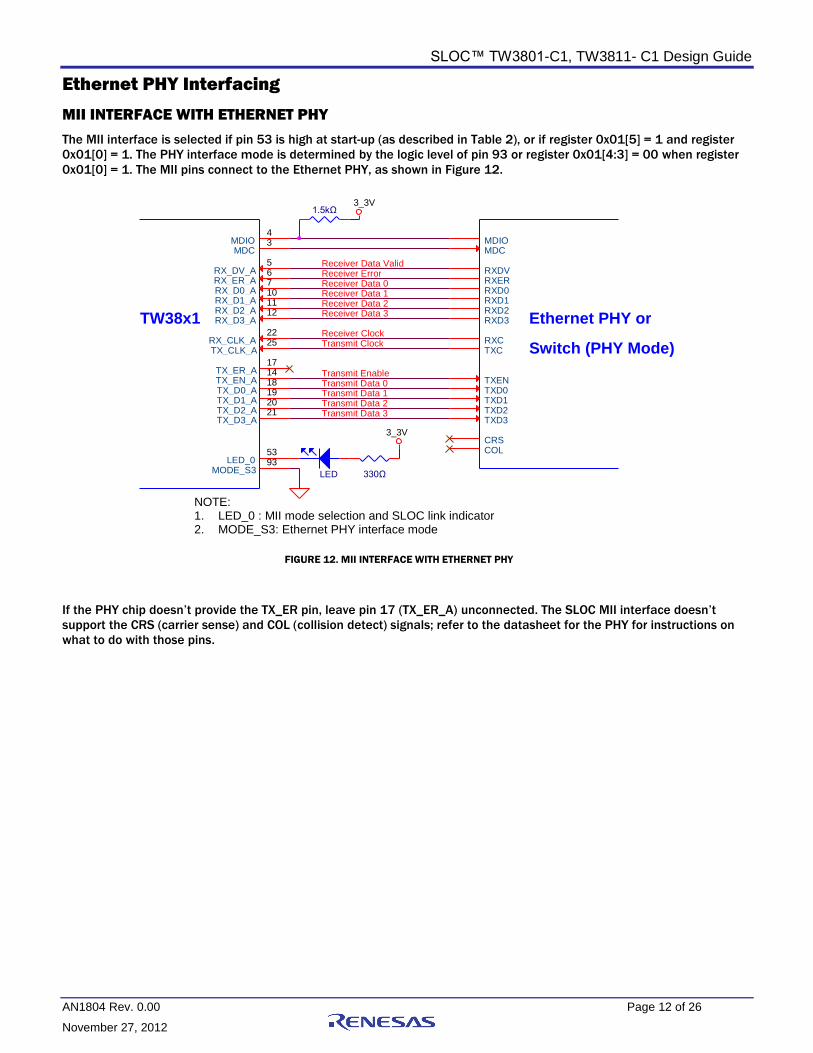
Ethernet PHY Interfacing
MII INTERFACE WITH ETHERNET PHY
The MII interface is selected if pin 53 is high at start-up (as described in Table 2), or if register 0x01[5] = 1 and register
0x01[0] = 1. The PHY interface mode is determined by the logic level of pin 93 or register 0x01[4:3] = 00 when register
0x01[0] = 1. The MII pins connect to the Ethernet PHY, as shown in Figure 12.
If the PHY chip doesn’t provide the TX_ER pin, leave pin 17 (TX_ER_A) unconnected. The SLOC MII interface doesn’t
support the CRS (carrier sense) and COL (collision detect) signals; refer to the datasheet for the PHY for instructions on
what to do with those pins.
Switch (PHY Mode)
330Ω
3_3V
LED
3_3V
TW38x1
RX_DV_A 5
RX_ER_A 6
RX_D0_A 7
RX_D1_A 10
RX_D2_A 11
RX_D3_A 12
TX_EN_A 14 TX_ER_A 17
TX_D0_A 18
TX_D1_A 19
TX_D2_A 20
TX_D3_A 21
RX_CLK_A 22
TX_CLK_A 25
MDC 3 MDIO 4
LED_0 53
MODE_S3 93
Ethernet PHY or
RXDV
RXD0 RXD1 RXD2 RXD3
RXC TXC
TXD0
TXD2 TXD3
TXEN
MDC MDIO
CRS COL
RXER
TXD1
Receiver Data 3 Receiver Data 2 Receiver Data 1 Receiver Data 0 Receiver Error Receiver Data Valid
Transmit Data 1 Transmit Data 0 Transmit Enable
Transmit Clock Receiver Clock
Transmit Data 3 Transmit Data 2
1.5kΩ
NOTE: 1. LED_0 : MII mode selection and SLOC link indicator 2. MODE_S3: Ethernet PHY interface mode
FIGURE 12. MII INTERFACE WITH ETHERNET PHY

SLOC™ TW3801-C1, TW3811- C1 Design Guide
AN1804 Rev. 0.00 Page 13 of 26
November 27, 2012
RMII INTERFACE WITH ETHERNET PHY
Some multi-channel PHY chips use the RMII interface instead of MII. RMII can be selected by keeping pin 53 (LED_0) low
at power-on/after reset or by setting register 0x01[5] = 0 with register 0x01[0] = 1. There are two different designs
depending on the source of the 50MHz RMII reference clock. If the 50MHz reference clock is coming from the Ethernet
PHY, connect as shown in Figure 13. Register 0x01[6] must be set to 1 to use external PHY clock (that is its default
setting).
Receive Error
50MHz Clock Reference
Transmit Data 1
Transmit Enable Switch (PHY Mode)
3_3V
TW38x1
RX_DV_A 5
RX_ER_A 6
RX_D0_A 7
RX_D1_A 10
TX_EN_A 14
TX_D0_A 18
TX_D1_A 19
TX_CLK_A 25
MDC 3 MDIO 4
LED_0 53
MODE_S3 93
Ethernet PHY or
CRS_DV
RXD0 RXD1
TXC
TXD0 TXEN
MDC MDIO
RXER
TXD1
Receive Data 0
Receive Data Valid
Transmit Data 0
Receive Data 1
1.5kΩ
2N3906 3
2 1 10kΩ
3_3V
330Ω
4.7kΩ
LED
NOTE: 1. LED_0 : RMII mode selection and SLOC link indicator 2. MODE_S3: Ethernet PHY interface mode
FIGURE 13. RMII INTERFACE WITH 50MHz REFERENCE CLOCK GENERATED BY PHY

SLOC™ TW3801-C1, TW3811- C1 Design Guide
AN1804 Rev. 0.00 Page 14 of 26
November 27, 2012
If the 50MHz reference clock is not provided from the Ethernet PHY, the SLOC chip can supply the clock from pin 50
(TEST_IO/CLK50M) with register 0x01[6] = 0. The RMII connections with 50MHz clock from SLOC chip are shown in
Figure 14.
50MHz Clock Reference
Receive Error
Switch (PHY Mode) Transmit Data 0
3_3V
TW38x1
RX_DV_A 5
RX_ER_A 6
RX_D0_A 7
RX_D1_A 10
TX_EN_A 14
TX_D0_A 18
TX_D1_A 19
TX_CLK_A 25
MDC 3 MDIO 4
LED_0 53
MODE_S3 93
TEST_IO/CLK50M 50
Receive Data 0
Receive Data Valid
Ethernet PHY or
CRS_DV
RXD0 RXD1
TXC
TXD0 TXEN
MDC MDIO
RXER
TXD1
Receive Data 1
1.5kΩ
Transmit Enable
10kΩ
3_3V
2N3906 3
2 1
330Ω
4.7kΩ
LED
Transmit Data 1
NOTE: 1. LED_0 : RMII mode selection and SLOC link indicator 2. MODE_S3: Ethernet PHY interface mode 3. Set register 0x01[6] = 0 for 50MHz reference clock output from pin #50
FIGURE 14. RMII INTERFACE WITH 50MHz REFERENCE CLOCK GENERATED BY SLOC

SLOC™ TW3801-C1, TW3811- C1 Design Guide
AN1804 Rev. 0.00 Page 15 of 26
November 27, 2012
PHY ADDRESS SETTINGS
When SLOC is in the PHY interface mode, the internal SLOC link state machine periodically checks the PHY link-status
register via the MDC/MDIO management signals. In the MDIO read sequence, the Ethernet PHY address is required.
SLOC generates the address of the PHY chip as a function of the SLOC chip’s I2C address and the value in register 0x1E,
bits[6:4] as follows:
Ethernet PHY address = SLOC register 0x1E bits[6:4] + logic level of Pins 57 and 56
Table 3 shows the first 8 of the 32 possible PHY addresses. The PHY address should be set per the PHY’s datasheet to
match the SLOC PHY address.
TABLE 3. ETHERNET PHY ADDRESS
ETHERNET PHY ADDRESS REG0X1E BIT 6-4 PIN # 57 PIN# 56
0 000 0 (Low) 0 (Low)
1 000 0 (Low) 1 (High)
2 000 1 (High) 0 (Low)
3 000 1 (High) 1 (High)
4 001 0 (Low) 0 (Low)
5 001 0 (Low) 1 (High)
6 001 1 (High) 0 (Low)
7 001 1 (High) 1 (High)
8 010 0 (Low) 0 (Low)
… … … …
ETHERNET PHY RESET APPLICATION
In early revisions of the SLOC IC, SLOC controlled the reset of the Ethernet PHY chip through pin 13. The TW3801C1 and
TW3811C1 do not need to control the PHY reset. Pin 13 can be left disconnected.

SLOC™ TW3801-C1, TW3811- C1 Design Guide
AN1804 Rev. 0.00 Page 16 of 26
November 27, 2012
SOC (CODEC) Chip Interfaces
MII INTERFACE WITH SOC
The MII interface mode is entered by taking pin 53 high during reset/power-on (see Figure 8) or setting register
0x01[5] = 1 with register 0x01[0] = 1. The SOC (CODEC) interface mode is set by tying pin 93 (MODE_S3) to 3.3V or
setting register 0x01[4:3] = 01 with register 0x01[0] = 1. The MII connections to the SOC should use the MIIB pins, as
shown in Figure 15. In this mode, the management interface (MDC/MDIO) is not required and the pins should be tied
high to 3.3V with 10kΩ resistors.
RMII INTERFACE WITH SOC
RMII mode is entered by taking pin 53 low during reset/power-on (see Figure 8) or setting register 0x01[5] = 0 with
register 0x01[0] = 1. Since a SOC (CODEC) chip typically doesn’t provide 50MHz reference clock, the 50MHz clock output
from pin 50 should be enabled with register 0x01[6] = 0. In this application, the 50MHz clock should also be sent to the
MIIA TX_CLK (pin 25) as shown in Figure 16.
TW38x1
TX_ER_B 26
TX_EN_B 29
TX_D0_B 30
TX_D1_B 31
TX_D2_B 32
TX_D3_B 33
RX_CLK_B 36 TX_CLK_B 37
RX_ER_B 38
RX_DV_B 39
RX_D0_B 40
RX_D1_B 41
RX_D2_B 44
RX_D3_B 45
MDIO 4
MDC 3
LED_0 53
MODE_S3 93
SOC (CODEC)
TX_ER TX_EN TXD0 TXD1 TXD2 TXD3
RX_CLK TX_CLK
RX_ER RX_DV RXD0 RXD1 RXD2 RXD3
Transmit Data 0
3_3V
Receiver Data 0
LED 330Ω
4.7kΩ
Transmit Enable Transmit Error
Transmit Data 1 Transmit Data 2 Transmit Data 3
Transmit Clock
Receiver Error
Receiver Clock
Receiver Data Valid
Receiver Data 1 Receiver Data 2 Receiver Data 3
10kΩ 3_3VD
10kΩ
NOTE: 1. LED_0 : MII mode selection and SLOC link indicator 2. MODE_S3: SOC (CODEC) interface mode
FIGURE 15. MII INTERFACE WITH SOC (CODEC) MODE

SLOC™ TW3801-C1, TW3811- C1 Design Guide
AN1804 Rev. 0.00 Page 17 of 26
November 27, 2012
ESD/EMI Solution
The SLOC chip will withstand electrostatic discharge up to 2kV (human body model). For higher protection on the
COAX_I/O pins, additional ESD protection can be added, as shown Figure 9. Since the SLOC signal range extends to over
40MHz, low capacitance ESD devices are required to avoid signal degradation. The capacitance of the devices should not
exceed 3pF. Two ESD devices have been tested and verified to work with SLOC:
EZAEG3A (Panasonic)
BV03CL (Bencent, China)
If EMI reduction is needed, an EMI filter can be placed on the SLOC_I/O port as well. When choosing any EMI/EMC
components, check the attenuation vs. frequency characteristics, and look for frequency-dependent impedance. The
SLOC signal should not be attenuated at 50MHz and below. To verify proper operation in COAX_IO path, contact Intersil
application team.
TW38x1
TX_EN_B 29
TX_D0_B 30
TX_D1_B 31
TX_CLK_A 25
RX_ER_B 38
RX_DV_B 39
RX_D0_B 40
RX_D1_B 41
MDIO 4
MDC 3
LED_0 53
MODE_S3 93
TEST_IO/CLK50M 50
SOC (CODEC)
TX_EN TXD0 TXD1
TX_CLK
RX_ER RX_DV RXD0 RXD1
Transmit Data 1
3_3V 4.7kΩ
Transmit Data 0 Transmit Enable
Receiver Data 1
Receiver Data Valid Receiver Error
10kΩ 3_3VD
10kΩ
50MHz Clock Reference
Receiver Data 0
3_3V
10kΩ 2N3906
3
2 1
330
LED
4.7kΩ
NOTE: 1. LED_0 : RMII mode selection and SLOC link indicator 2. MODE_S3: SOC(CODEC) interface mode 3. Set register 0x01[6] = 0 for 50MHz reference clock output from pin 50
FIGURE 16. RMII INTERFACE WITH SOC (CODEC) MODE

SLOC™ TW3801-C1, TW3811- C1 Design Guide
AN1804 Rev. 0.00 Page 18 of 26
November 27, 2012
SLOC Firmware The TW3801 and TW3811 have been designed to work stand-alone (without an external micro-controller) in many
applications. The default register settings are optimized for stand-alone operation, with external pins available to change
the most popular settings.
However, it is possible to program additional registers inside the TW3801 and TW3811 using the I2C interface, including
override the settings set by the external pins. Table 4 (TW3801) and Table 5 (TW3811) explain how to change the
interface mode via software (vs the hardware pins as described in “SLOC Downlink/Uplink Throughput Settings” on
page 7 and “Data Rate Vs Cable Length” on page 8). After the new interface mode is programmed, the device must be
“soft” reset by writing a 1 to register 0 bit 0 before the new interface mode will be used. Please refer to the datasheet for
additional information on user I2C registers.
TABLE 4. TW3801 DEVICE
INTERFACE OPERATING MODE I2C SETTINGS PROCEDURE
MII interface
Ethernet PHY interface Mode
Register 0x01 = 0x61
Register 0x0A = 0x13: required manual speed setting
(e.g. 36Mbps)
Register 0x00 = 0x01: soft reset
SOC interface Mode Register 0x01 = 0x69
Same settings are required in Reg0x0A/0x00
Pass-Through Mode Register 0x01 = 0x71
Same settings are required in Reg0x0A/0x00
RMII interface with
internal 50MHz clock
Ethernet PHY interface Mode Register 0x01 = 0x01
Same settings are required in Reg0x0A/0x00
SOC interface Mode Register 0x01 = 0x09
Same settings are required in Reg0x0A/0x00
Pass-Through Mode Register 0x01 = 0x11
Same settings are required in Reg0x0A/0x00
RMII interface with
external 50MHz clock
Ethernet PHY interface Mode Register 0x01 = 0x41
Same settings are required in Reg0x0A/0x00
SOC interface Mode Register 0x01 = 0x49
Same settings are required in Reg0x0A/0x00
Pass-Through Mode Register 0x01 = 0x51
Same settings are required in Reg0x0A/0x00
SLOC™ TW3801-C1, TW3811- C1 Design Guide
AN1804 Rev. 0.00 Page 19 of 26
November 27, 2012
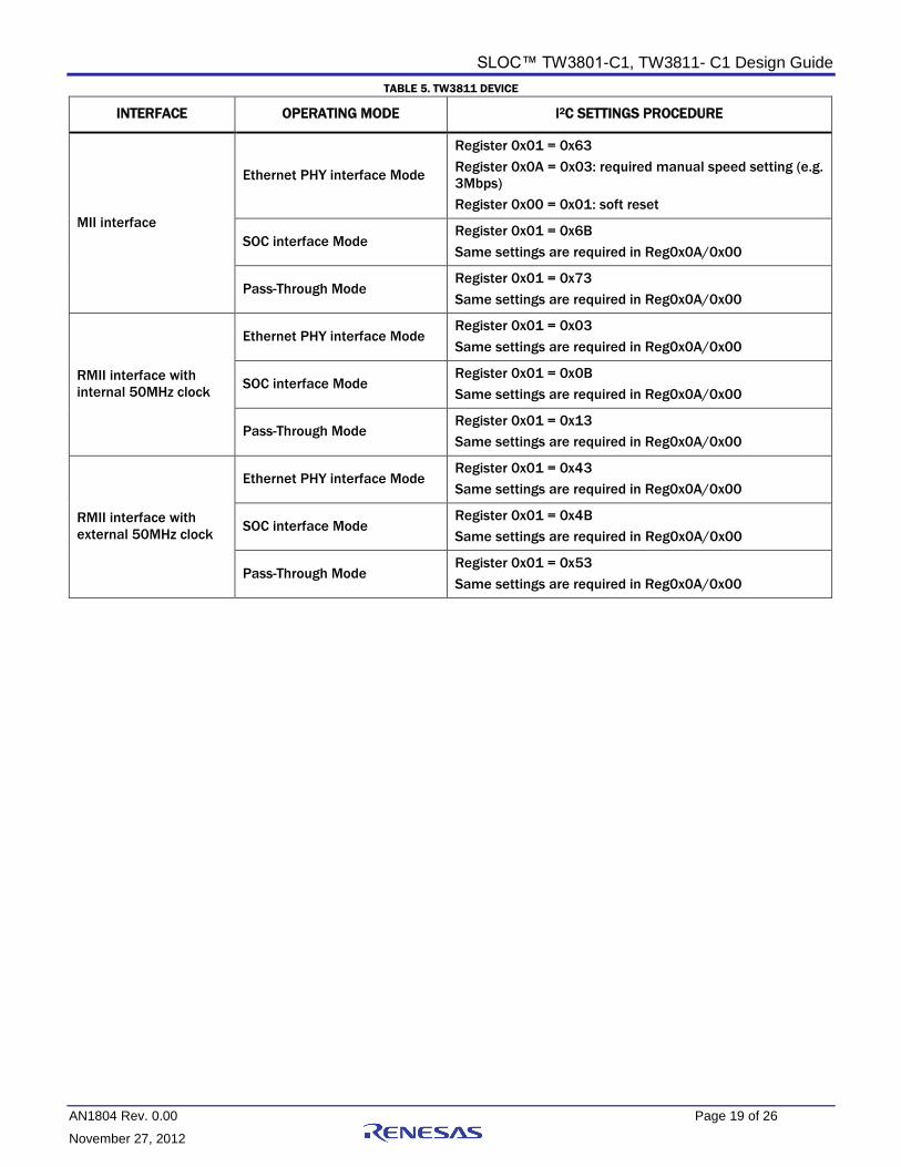
TABLE 5. TW3811 DEVICE
INTERFACE OPERATING MODE I2C SETTINGS PROCEDURE
MII interface
Ethernet PHY interface Mode
Register 0x01 = 0x63
Register 0x0A = 0x03: required manual speed setting (e.g.
3Mbps)
Register 0x00 = 0x01: soft reset
SOC interface Mode Register 0x01 = 0x6B
Same settings are required in Reg0x0A/0x00
Pass-Through Mode Register 0x01 = 0x73
Same settings are required in Reg0x0A/0x00
RMII interface with
internal 50MHz clock
Ethernet PHY interface Mode Register 0x01 = 0x03
Same settings are required in Reg0x0A/0x00
SOC interface Mode Register 0x01 = 0x0B
Same settings are required in Reg0x0A/0x00
Pass-Through Mode Register 0x01 = 0x13
Same settings are required in Reg0x0A/0x00
RMII interface with
external 50MHz clock
Ethernet PHY interface Mode Register 0x01 = 0x43
Same settings are required in Reg0x0A/0x00
SOC interface Mode Register 0x01 = 0x4B
Same settings are required in Reg0x0A/0x00
Pass-Through Mode Register 0x01 = 0x53
Same settings are required in Reg0x0A/0x00

SLOC™ TW3801-C1, TW3811- C1 Design Guide
AN1804 Rev. 0.00 Page 20 of 26
November 27, 2012
SLOC Performance Check
PER (Packet Error Rate) Measurement
The SLOC chip can measure PER to check for any errors which may have occurred across the COAX link.
DOWNLINK PER
The PER should be measured in TW3811 with below register settings after the SLOC link is completed (The LED from
LED_0 Pin# 53 is turned on or register 0x44 bit[5] = 1).
1. Write register 0x27 to 0x00 (Reset the PER measurement)
2. Write packet counter number into register 0x27. The number indicates 65536 packets per value. If 0x05 in the
register is written, a total 327680 (5 x 65536) packets are measured.
3. Monitor register 0x43 bit[0] if it is 1. If it is 0, the error measurement is not completed.
4. After confirmed register 0x43 bit[0] = 1, read register 0x42 to 0x40. The return values of the registers are the
packet error number.
Register 0x40[7:0] = Error count[7:0]
Register 0x41[7:0] = Error count[15:8]
Register 0x42[7:0] = Error count[23:16]
5. The values should be all zero. If not, the SLOC link generates an error and some video data will be lost.
UPLINK PER
The PER should be measured in TW3801 after the SLOC link is completed. The process to evaluate the error packets is
same as downlink PER one.
SLOC Signals Evaluation
For SLOC signal evaluation, refer to the SLOC compliance document.

SLOC™ TW3801-C1, TW3811- C1 Design Guide
AN1804 Rev. 0.00 Page 21 of 26
November 27, 2012
PCB Layout Guide
COAX_OUT and COAX_IN
The SLOC ICs generate a wide-band multiplexed signal consisting of two modulated signals and base-band CVBS
extending over a 0 to 42MHz range. It is important to route the signal traces carefully to minimize distortion and
crosstalk, and achieve maximum COAX cable length.
Routing advice:
Place components (coupling capacitors and load resistor) so that the traces are as straight and short as possible.
Avoid right-angle bends in the traces to minimize signal reflection. Use a 45° design rule.
Traces should have a characteristic impedance of 75Ω impedance. Other than 75Ω will increase reflections and
affect signal quality.
Breaks in the ground plane can also cause impedance mismatch – make sure all high speed signals run over a
constant ground plane.
Avoid vias – they also introduce impedance mismatch.
Avoid routing the traces near digital signals and clock traces.
To avoid unwanted coupling between COAX_OUT and COAX_IN traces, keep the spacing as far apart as possible
until they are combined (after the coupling capacitors)
Don’t make a “T” as shown below. This degrades return loss and may reduce maximum COAX cable length.
BAD EXAMPLE
WIDEN
SPACING
DON’T MAKE BRANCH WITHIN TRACE
COAX_OUT
COAX_IN
SLOC™ TW3801-C1, TW3811- C1 Design Guide
AN1804 Rev. 0.00 Page 22 of 26
November 27, 2012
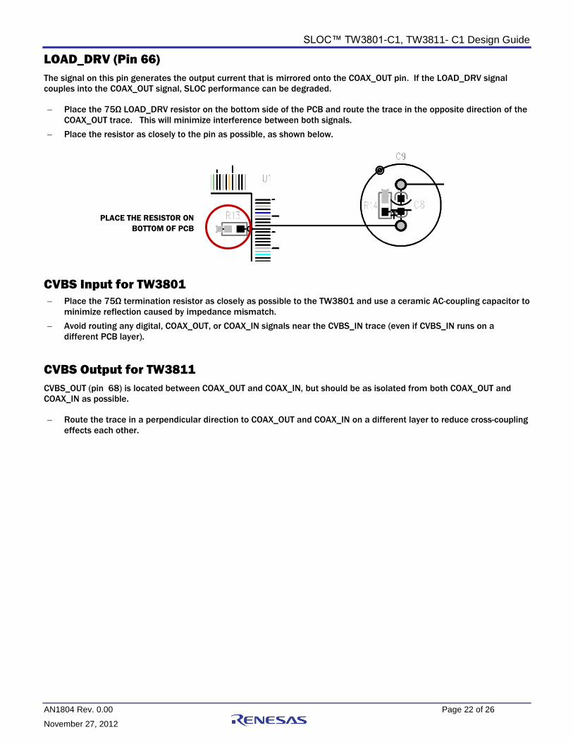
LOAD_DRV (Pin 66)
The signal on this pin generates the output current that is mirrored onto the COAX_OUT pin. If the LOAD_DRV signal
couples into the COAX_OUT signal, SLOC performance can be degraded.
Place the 75Ω LOAD_DRV resistor on the bottom side of the PCB and route the trace in the opposite direction of the
COAX_OUT trace. This will minimize interference between both signals.
Place the resistor as closely to the pin as possible, as shown below.
CVBS Input for TW3801
Place the 75Ω termination resistor as closely as possible to the TW3801 and use a ceramic AC-coupling capacitor to
minimize reflection caused by impedance mismatch.
Avoid routing any digital, COAX_OUT, or COAX_IN signals near the CVBS_IN trace (even if CVBS_IN runs on a
different PCB layer).
CVBS Output for TW3811
CVBS_OUT (pin 68) is located between COAX_OUT and COAX_IN, but should be as isolated from both COAX_OUT and
COAX_IN as possible.
Route the trace in a perpendicular direction to COAX_OUT and COAX_IN on a different layer to reduce cross-coupling
effects each other.
PLACE THE RESISTOR ON
BOTTOM OF PCB

SLOC™ TW3801-C1, TW3811- C1 Design Guide
AN1804 Rev. 0.00 Page 23 of 26
November 27, 2012
Power Distribution
The SLOC ICs require two regulated supply voltages: 1.8V for digital core and 3.3V for analog and digital I/O. Since the
3.3V for analog and digital I/O usually comes from the same regulator, the power traces (or planes) should be designed
to minimize the common impedance. Also, the spacing between the digital and analog power traces (or plane) should be
enough to reduce unwanted coupling (25mils or more).
FERRITE
BEAD
POOR EXAMPLE
3.3V
REGU.
COMMON
IMPEDANCE
DIGITAL I/O 3.3V ANALOG 3.3V
TW38x1
FERRITE
BEAD
3.3V
REGU.
MINIMIZE
COMMON
IMPEDANCE
ANALOG 3.3V DIGITAL I/O 3.3V
BETTER EXAMPLE
TAKE ENOUGH
SPACE BETWEEN
POWER PLANES
TW38x1

SLOC™ TW3801-C1, TW3811- C1 Design Guide
AN1804 Rev. 0.00 Page 24 of 26
November 27, 2012
Decoupling Capacitors for Power Pins
All power pins should have a 0.1µF capacitor decoupling on their supply lines, with the capacitors placed as close to the
VDD and analog power pins as possible. When power is supplied through a via, avoid placing the via between the
capacitor and the power pin. Current should flow from power plane (trace) -> decoupling capacitor -> power pin, as shown
below.
Ground Considerations
Intersil recommends a single ground under the TW3801/TW3811 to avoid ground potential differences between analog
and digital ground pins. However, it is also important to prevent the ground current from one source (such as the crystal
oscillator) to couple into the ground current of another group (i.e. analog). To satisfy both requirements, one technique is
to partially split the GND plane around a noise source to direct the current. For example:
CLOSE
TW3801/11
DECOUPLING CAPACITOR
SINGLE GND
UNDER CHIP
SPLIT GND ABOVE
NOISE SOURCE

SLOC™ TW3801-C1, TW3811- C1 Design Guide
AN1804 Rev. 0.00 Page 25 of 26
November 27, 2012
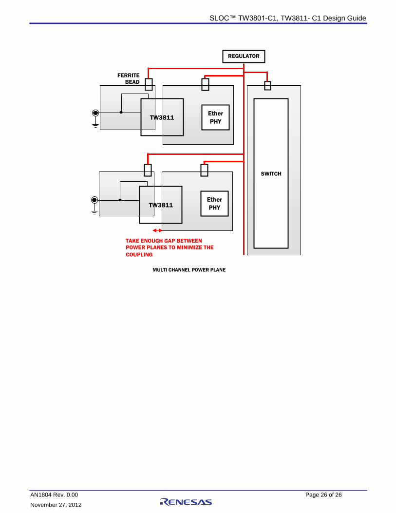
Multi-Channel Design
For a multi-channel (NVR. DVR, etc.) SLOC design, additional steps should be taken to achieve the best performance. It is
important to avoid coupling not only between up- and down-link signals, but also between each channel. Separate power
and ground planes between each channel, joined together at the common point (in this case the switch) are necessary.
…
DON’T USE
COMMON GROUND
BETWEEN
CHANNELS
WIDEN
SPACING
BETWEEN
EACH CHANNEL
SLOC SIGNALS
Ether
PHY
Ether
PHY TW3811
TW3811 Switch
GROUND
MULTI CHANNEL GROUND PLANE
SLOC™ TW3801-C1, TW3811- C1 Design Guide
AN1804 Rev. 0.00 Page 26 of 26
November 27, 2012
MULTI CHANNEL POWER PLANE
REGULATOR
SWITCH
Ether
PHY TW3811
FERRITE
BEAD
Ether
PHY TW3811
TAKE ENOUGH GAP BETWEEN
POWER PLANES TO MINIMIZE THE
COUPLING