Embed Size (px)
Citation preview

Slide Set 14, Page 1
Slide Set 14
Design for Testability
Steve WiltonDept. of ECE
University of British [email protected]
Slide Set 14, Page 2
Overview
Wolf 4.8, 5.6, 5.7, 8.7
Up to this point in the class, we have spent all of time trying to figure out what we want on a chip, how to implement the desired functionality. We also need to figure out a method of testing to see if the chip works after it is manufactured. There are two types of testing a designer is interested in. The first is to check out the design, to make sure it is correct, and implements the desired functionality. We have talked some about this testing already.Unfortunately the manufacturing process for ICs is not perfect, so we need to check each chip created to see if it matches the original design. Given the complexity of today’s chips, this can be a very difficult task, unless some planning is done up front. This planning is called design for testability.
Slide Set 14, Page 3
Types of Testing
1. Verification: Testing your design to make sure it is correct- Done using simulators (HSPICE, Verilog, IRSIM, etc.)- Usually follow a test plan written by Verification Engineers- Involves both testing Verilog code and final layout
2. Validation: Test every chip to see if it works- You are assuming your design is correct- Fabrication errors, imperfections in silicon cause errors- Don’t want to sell faulty chips!
3. Debugging: Why doesn’t this chip work?- So you can correct it in the next “spin”

Verification

103
Number of starsin the universe
Number of protonsin the universe
Number of latchesin Itanium processor
1 10 100 1000 100001
103000
10300
1030
100000 1000000
World population
Number of Storage Elements
Num
ber o
f Sta
tes
From J. Abraham, Oct 2005
Slide Set 14, Page 6
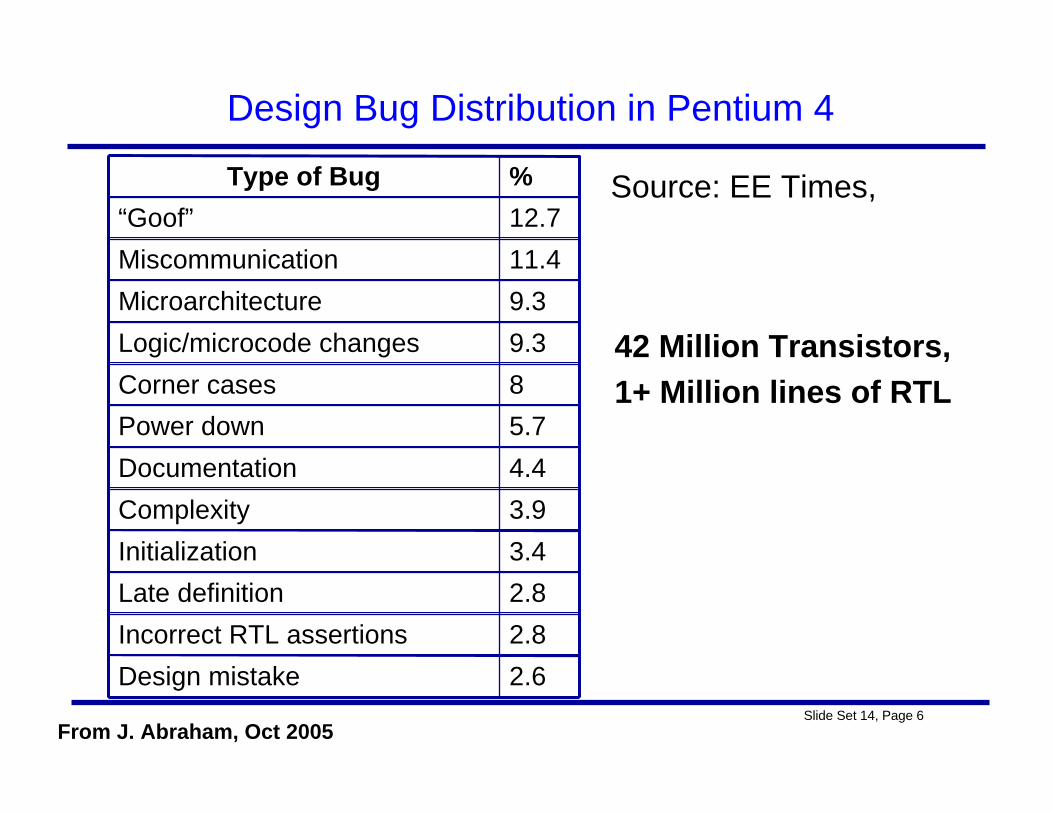
Design Bug Distribution in Pentium 4
2.6Design mistake2.8Incorrect RTL assertions2.8Late definition3.4Initialization3.9Complexity4.4Documentation5.7Power down8Corner cases9.3Logic/microcode changes9.3Microarchitecture11.4Miscommunication12.7“Goof”%Type of Bug
42 Million Transistors,1+ Million lines of RTL
Source: EE Times,
From J. Abraham, Oct 2005
Slide Set 14, Page 7
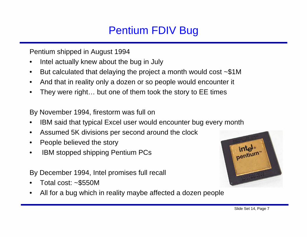
Pentium FDIV Bug
Pentium shipped in August 1994• Intel actually knew about the bug in July• But calculated that delaying the project a month would cost ~$1M• And that in reality only a dozen or so people would encounter it• They were right… but one of them took the story to EE times
By November 1994, firestorm was full on• IBM said that typical Excel user would encounter bug every month• Assumed 5K divisions per second around the clock• People believed the story• IBM stopped shipping Pentium PCs
By December 1994, Intel promises full recall• Total cost: ~$550M• All for a bug which in reality maybe affected a dozen people

TOP TEN NEW INTEL SLOGANS FOR THE PENTIUM--------------------------------------------------------------------------• 9.9999973251 It's a FLAW, Dammit, not a Bug• 8.9999163362 It's Close Enough, We Say So• 7.9999414610 Nearly 300 Correct Opcodes• 6.9999831538 You Don't Need to Know What's Inside• 5.9999835137 Redefining the PC -- and Mathematics As Well• 4.9999999021 We Fixed It, Really• 3.9998245917 Division Considered Harmful - No Life-Maintenance
Devices Should Be Used With This Processor• 2.9991523619 Why Do You Think They Call It *Floating* Point?• 1.9999103517 We're Looking for a Few Good Flaws
And the 0.9999999998th Slogan Is...
• The Errata Inside
Moral:Test your chip thoroughly.If you don’t test it, it won’t work. Guaranteed!
But, even if your design is correct, the chips that come back fromthe fab might not work

Validation

Slide Set 14, Page 11
Defects in Fabrication
In the fabrication of chips, there are defects that get introduced. These defects come from many sources:
– Defects in the base silicon.
– Dust or contamination in the fab or on wafer.
– Dust on mask.
– Misalignment.
– Over-etch or under-etch....→ sometimes you don't get the exact pattern you printed due to
limitations in the photolithographic process as we reach limits on resolution.
Thus, sometimes, the implementation of the fabricated die doesn’t match its specification, and you get wires you don’t want, don’t get wires that you want, or find out that the transistors don’t operate as you expect
Slide Set 14, Page 12
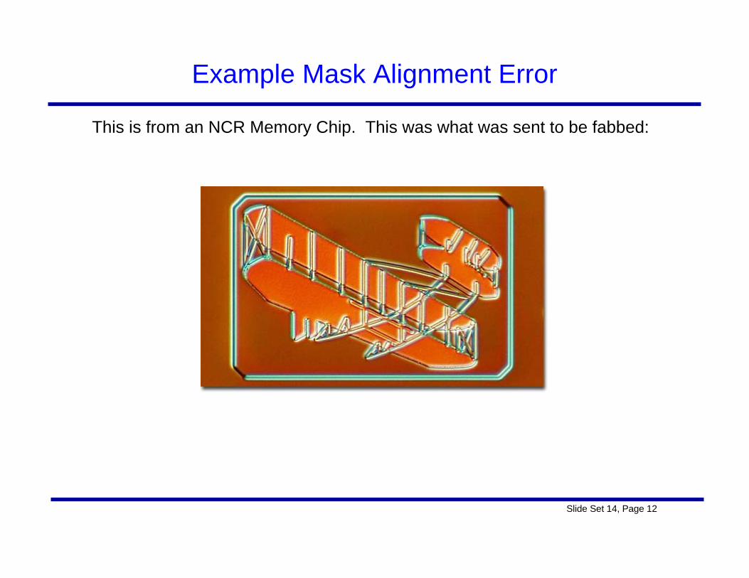
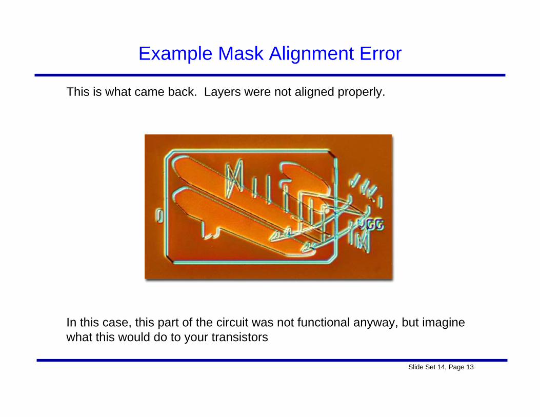
Example Mask Alignment Error
This is from an NCR Memory Chip. This was what was sent to be fabbed:
Slide Set 14, Page 13
Example Mask Alignment Error
This is what came back. Layers were not aligned properly.
In this case, this part of the circuit was not functional anyway, but imagine what this would do to your transistors

Slide Set 14, Page 14
Particle Defects
Particles can disrupt either “light-field” or “dark-field” patterns on the mask or on the wafer during photolithographic process.
Slide Set 14, Page 15
Remember this distinction: Verification vs. Validation
Verification: - Test your design- You can take advantage of regularity
- if one bit of a register works, they probably all do
Verification: - Test the actual chip- A fault could occur in any bit of a register… test them all- Need to test every chip you intend to sell
Slide Set 14, Page 16
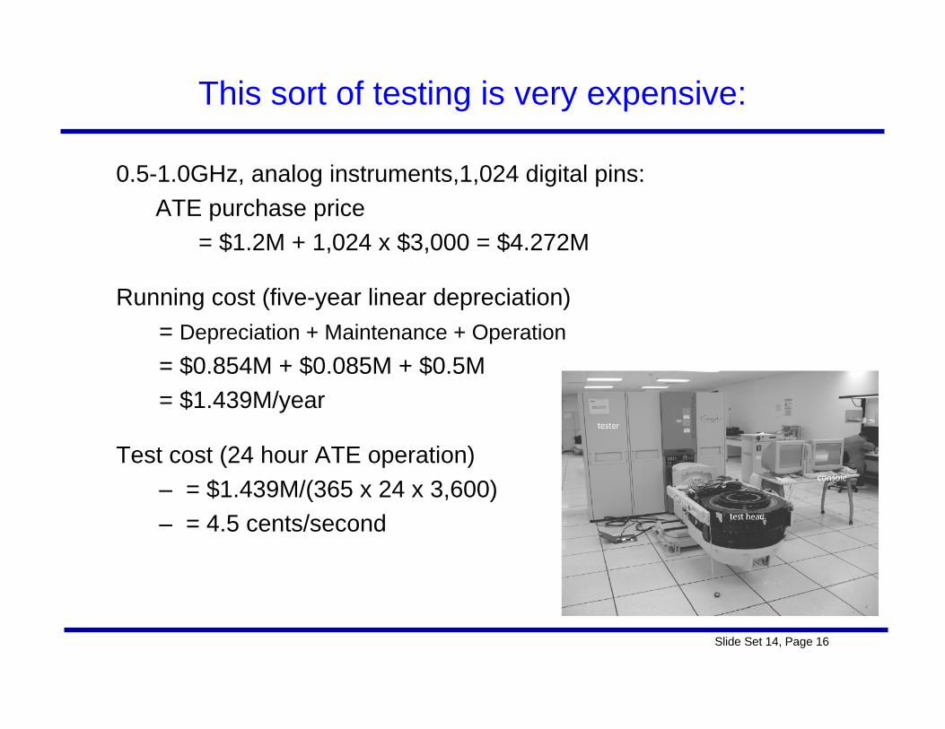
This sort of testing is very expensive:
0.5-1.0GHz, analog instruments,1,024 digital pins: ATE purchase price
= $1.2M + 1,024 x $3,000 = $4.272M
Running cost (five-year linear depreciation)= Depreciation + Maintenance + Operation= $0.854M + $0.085M + $0.5M= $1.439M/year
Test cost (24 hour ATE operation)– = $1.439M/(365 x 24 x 3,600)– = 4.5 cents/second
Slide Set 14, Page 17
Production Testing
Once the design is fully correct, production testing verifies correctfabrication for each new die.
But this isn’t trivial:1. Need to test all the gates in a chip.2. Only get to force chip inputs and observe chip outputs.
(Production testing is done with automated equipment, never microprobing or e-beam, obviously)
# gates >> # inputs/outputs.3. Production testing is always done by applying a sequence of vectors
(apply new input to pins, and measure outputs from pins), usually one vector per clock cycle.
If there were no internal states, the problem would merely be hard, but not impossible. With states, the problem is nearly impossible unless the designer helps.
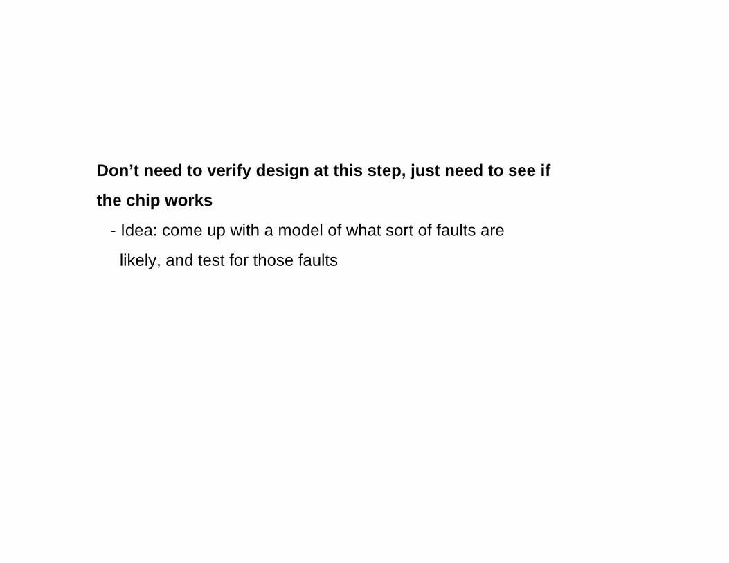
Don’t need to verify design at this step, just need to see if
the chip works
- Idea: come up with a model of what sort of faults are
likely, and test for those faults
Slide Set 14, Page 19
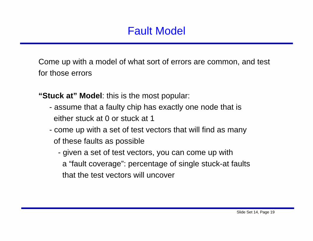
Fault Model
Come up with a model of what sort of errors are common, and testfor those errors
“Stuck at” Model: this is the most popular:- assume that a faulty chip has exactly one node that iseither stuck at 0 or stuck at 1
- come up with a set of test vectors that will find as manyof these faults as possible- given a set of test vectors, you can come up with a “fault coverage”: percentage of single stuck-at faultsthat the test vectors will uncover
Slide Set 14, Page 20
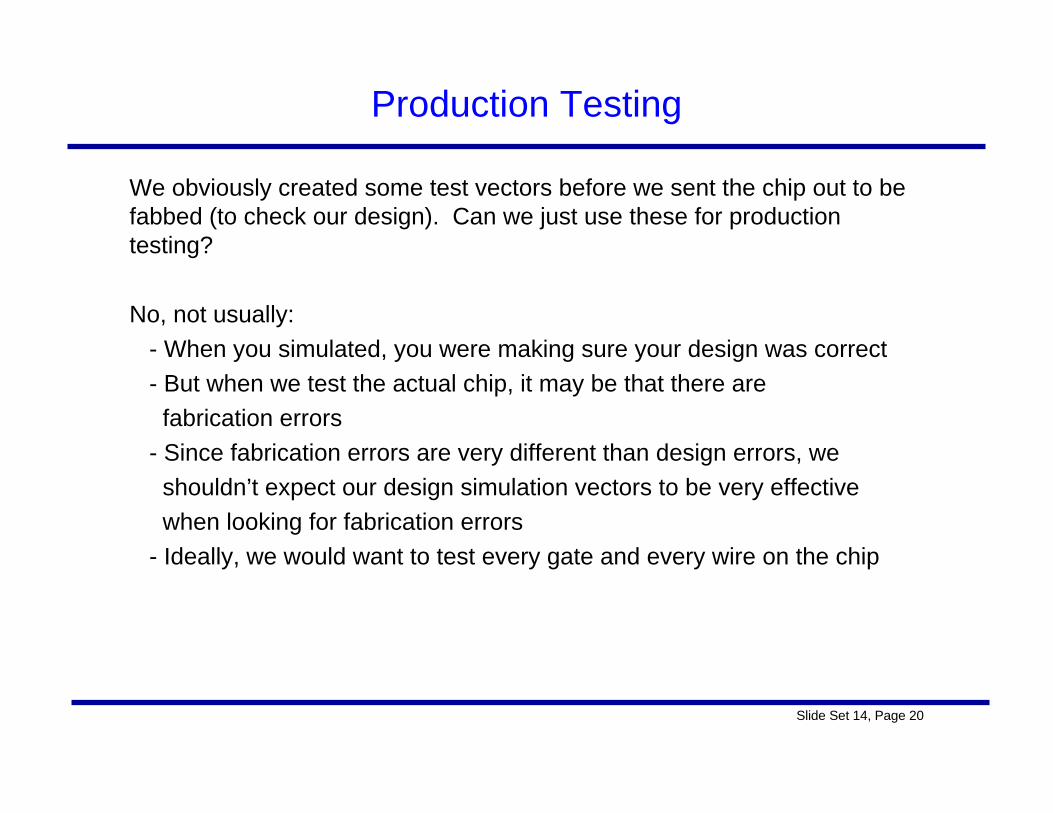
Production Testing
We obviously created some test vectors before we sent the chip out to be fabbed (to check our design). Can we just use these for production testing?
No, not usually:- When you simulated, you were making sure your design was correct- But when we test the actual chip, it may be that there are
fabrication errors- Since fabrication errors are very different than design errors, we
shouldn’t expect our design simulation vectors to be very effectivewhen looking for fabrication errors
- Ideally, we would want to test every gate and every wire on the chip
Slide Set 14, Page 21
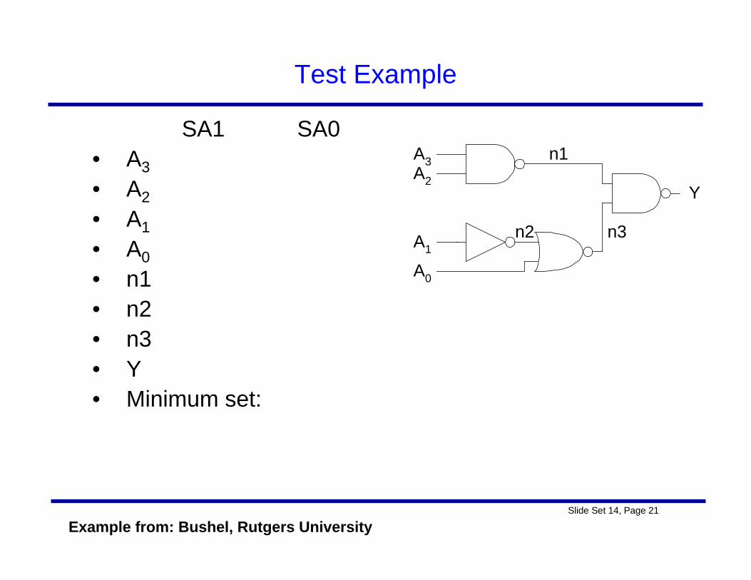
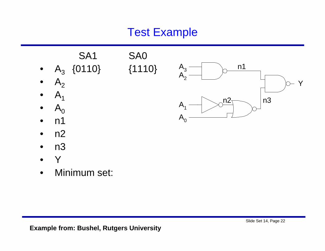
Test Example
SA1 SA0• A3• A2• A1• A0• n1• n2• n3• Y• Minimum set:
A3A2
A1
A0
Y
n1
n2 n3
Example from: Bushel, Rutgers University
Slide Set 14, Page 22
Test Example
SA1 SA0• A3 {0110} {1110}• A2• A1• A0• n1• n2• n3• Y• Minimum set:
A3A2
A1
A0
Y
n1
n2 n3
Example from: Bushel, Rutgers University

Slide Set 14, Page 23
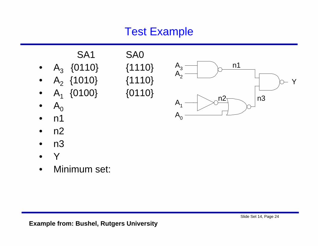
Test Example
SA1 SA0• A3 {0110} {1110}• A2 {1010} {1110}• A1• A0• n1• n2• n3• Y• Minimum set:
A3A2
A1
A0
Y
n1
n2 n3
Example from: Bushel, Rutgers University
Slide Set 14, Page 24
Test Example
SA1 SA0• A3 {0110} {1110}• A2 {1010} {1110}• A1 {0100} {0110}• A0• n1• n2• n3• Y• Minimum set:
A3A2
A1
A0
Y
n1
n2 n3
Example from: Bushel, Rutgers University
Slide Set 14, Page 25
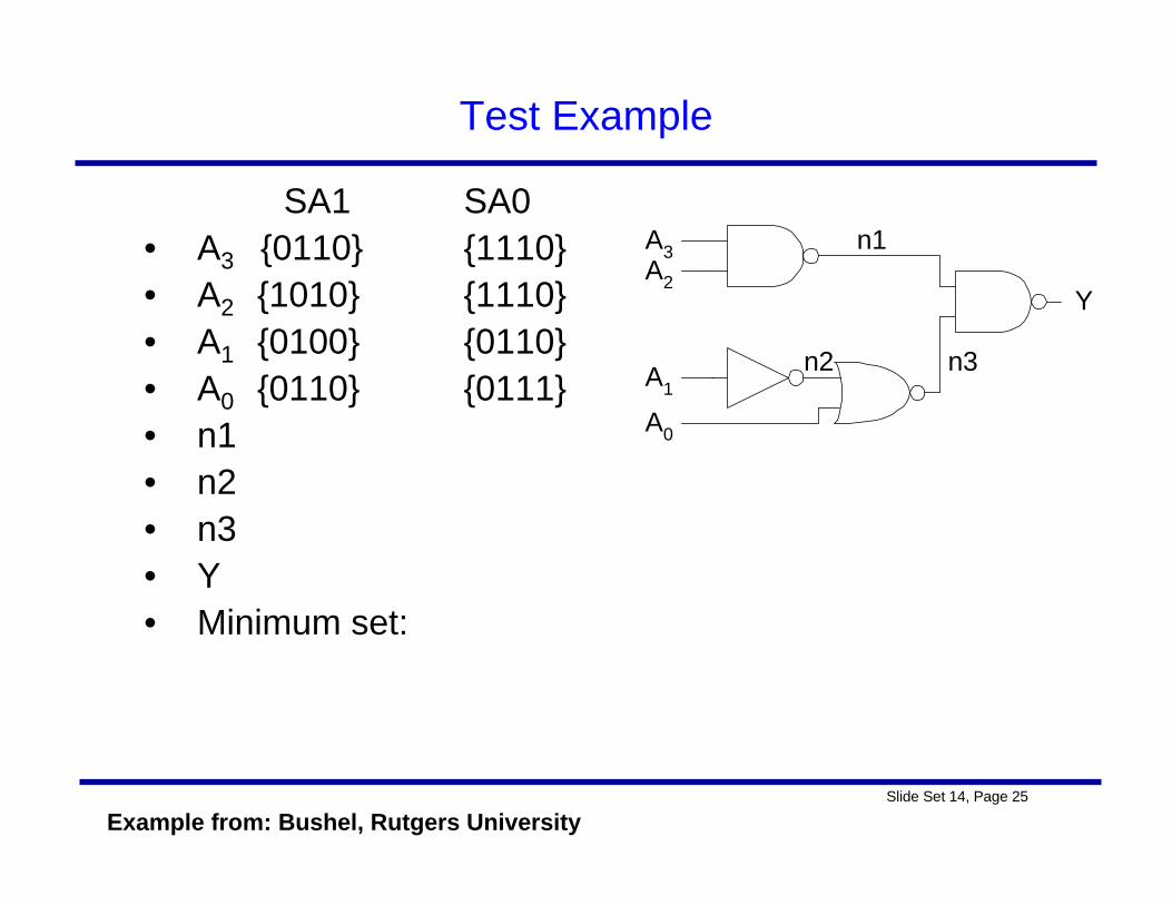
Test Example
SA1 SA0• A3 {0110} {1110}• A2 {1010} {1110}• A1 {0100} {0110}• A0 {0110} {0111}• n1• n2• n3• Y• Minimum set:
A3A2
A1
A0
Y
n1
n2 n3
Example from: Bushel, Rutgers University
Slide Set 14, Page 26
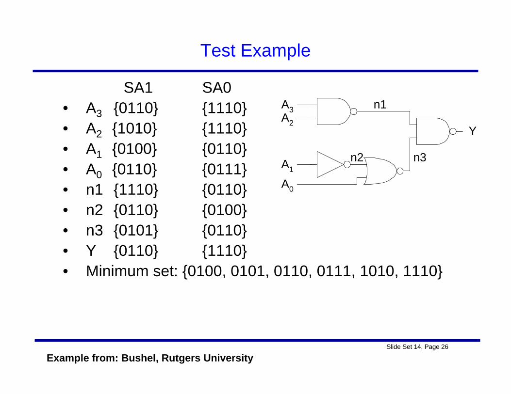
Test Example
SA1 SA0• A3 {0110} {1110}• A2 {1010} {1110}• A1 {0100} {0110}• A0 {0110} {0111}• n1 {1110} {0110}• n2 {0110} {0100}• n3 {0101} {0110}• Y {0110} {1110}• Minimum set: {0100, 0101, 0110, 0111, 1010, 1110}
A3A2
A1
A0
Y
n1
n2 n3
Example from: Bushel, Rutgers University
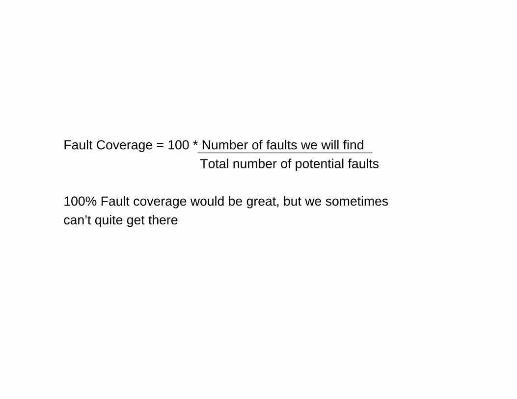
Fault Coverage = 100 * Number of faults we will findTotal number of potential faults
100% Fault coverage would be great, but we sometimes can’t quite get there
Slide Set 14, Page 28
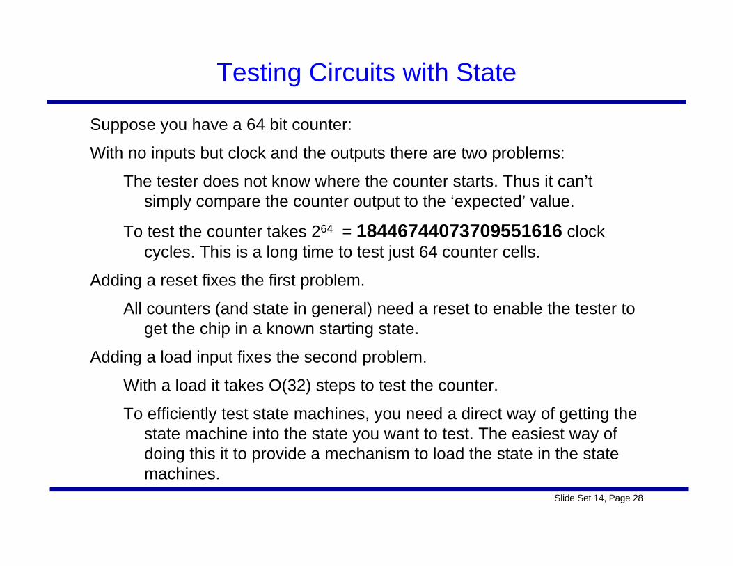
Testing Circuits with State
Suppose you have a 64 bit counter:
With no inputs but clock and the outputs there are two problems:
The tester does not know where the counter starts. Thus it can’t simply compare the counter output to the ‘expected’ value.
To test the counter takes 264 = 18446744073709551616 clock cycles. This is a long time to test just 64 counter cells.
Adding a reset fixes the first problem.
All counters (and state in general) need a reset to enable the tester to get the chip in a known starting state.
Adding a load input fixes the second problem.
With a load it takes O(32) steps to test the counter.
To efficiently test state machines, you need a direct way of getting the state machine into the state you want to test. The easiest way of doing this it to provide a mechanism to load the state in the state machines.
Slide Set 14, Page 29
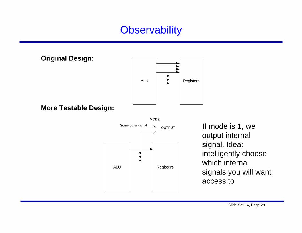
Observability
Original Design:
More Testable Design:
ALU Registers
ALU Registers
MODE
OUTPUTSome other signal If mode is 1, we
output internal signal. Idea: intelligently choose which internal signals you will want access to
Slide Set 14, Page 30
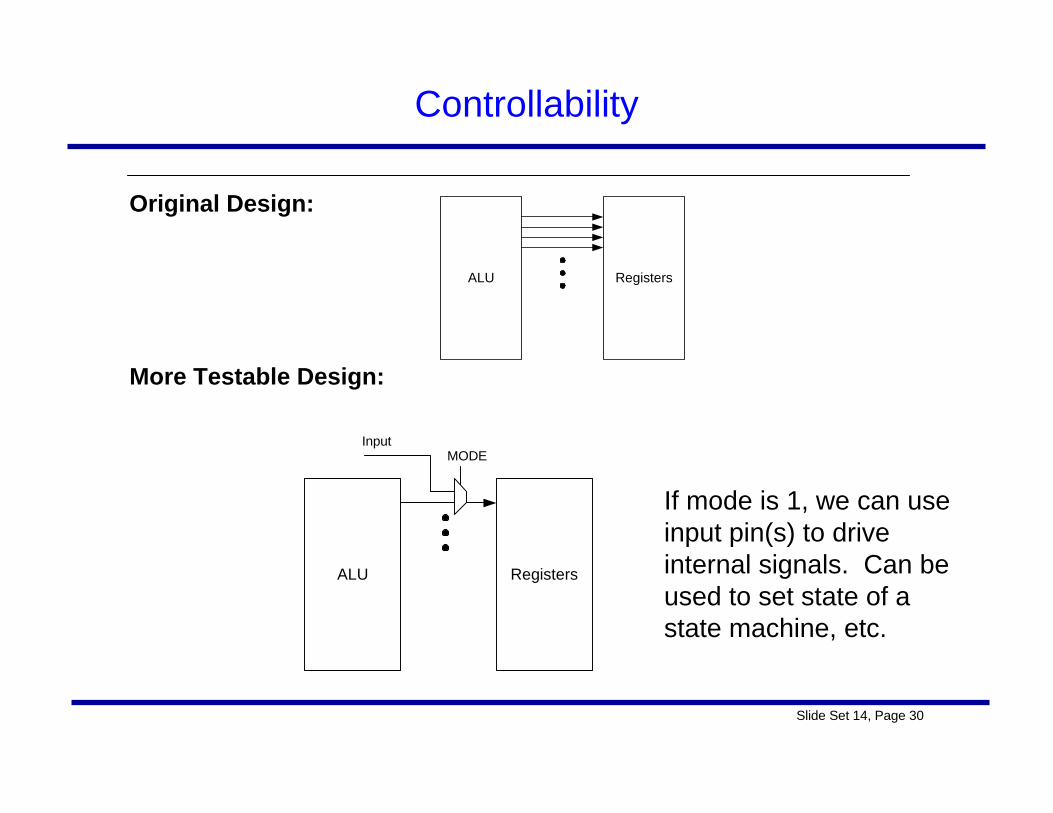
Controllability
Original Design:
More Testable Design:
ALU Registers
If mode is 1, we can use input pin(s) to drive internal signals. Can be used to set state of a state machine, etc.
ALU Registers
MODEInput
Slide Set 14, Page 31
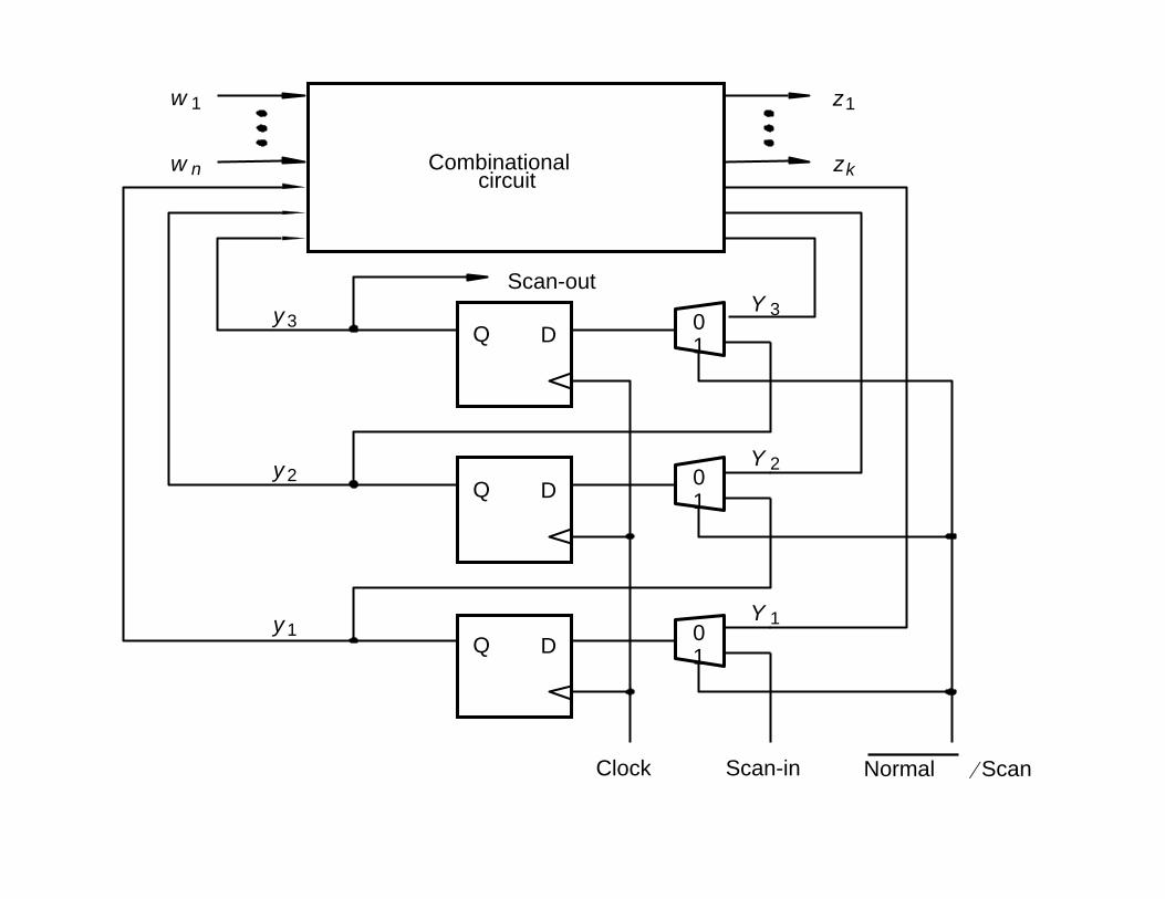
Scan
Scan techniques are often used in testing, since they take only a few (about 4 to 6) additional pins, but have the potential to control a lots of things (state, other output pads, etc.). Trade bandwidth for pins. Techniques requiring everything to be scannable are often called by the buzzword LSSD (level-sensitive scan design) which really just means “full-scan”. (Original meaning also implied strict 2 phase clocking)
• Convert testing a sequential machine into solely the problem of testing a block of combinational logic with ALL primary inputs controllable through scan, and all primary outputs observable through scan.
• Accomplish this by changing all the state latches into a latch that can become a shift-register, and linking them all together in scan chains.
• A state can be shifted in, all the logic can compute, and then the state can be shifted out at the same time the next state is shifted in. Do a complete scan between every applied test vector.
• Scan great for both debug and production wafer or packaged part testing• Partial-scan is possible, but ATPG tools are not as automated.
Slide Set 14, Page 32
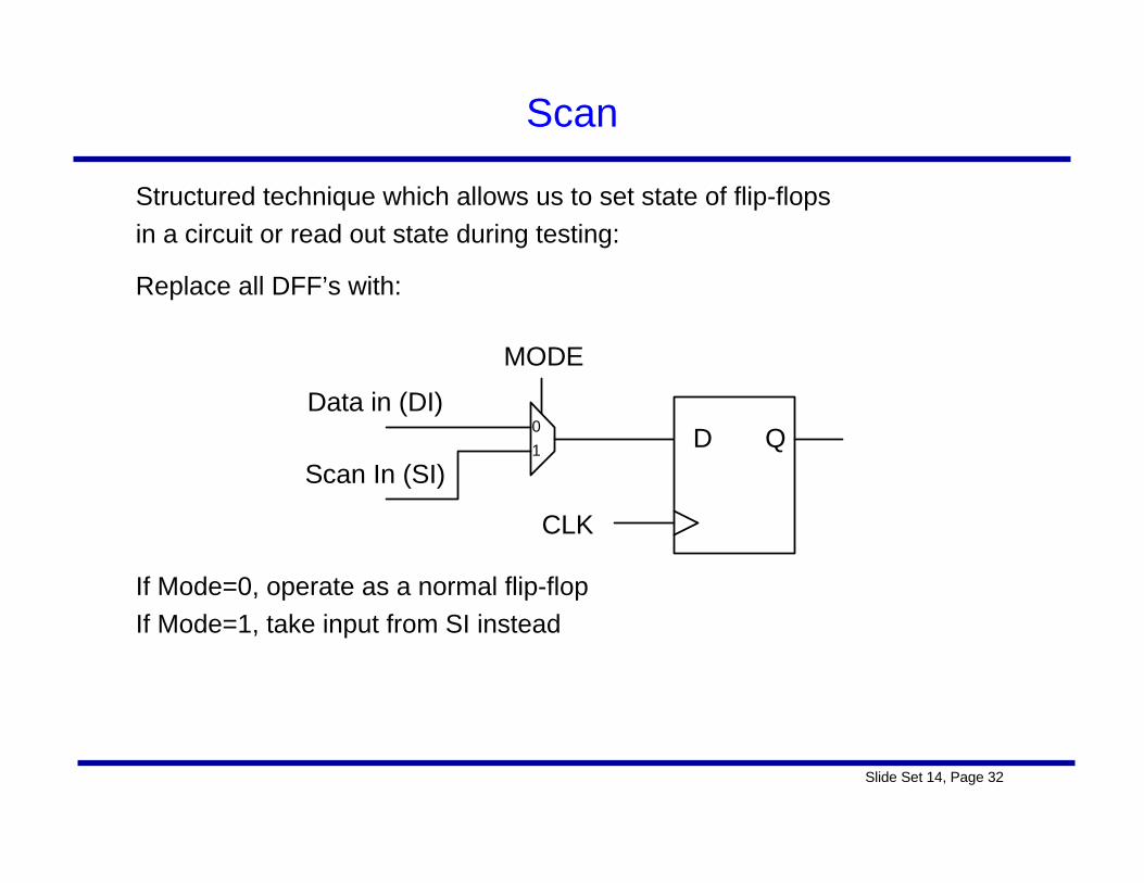
Scan
Structured technique which allows us to set state of flip-flopsin a circuit or read out state during testing:
Replace all DFF’s with:
If Mode=0, operate as a normal flip-flopIf Mode=1, take input from SI instead
MODE
Data in (DI)D Q
Scan In (SI)
01
CLK
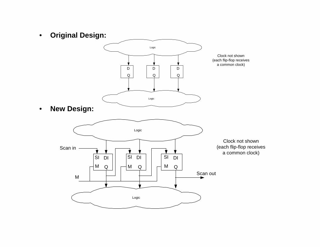
• Original Design:
• New Design:
D
Q
D
Q
D
Q
Logic
Logic
Clock not shown(each flip-flop receives
a common clock)
DI
Q Q Q
Logic
Logic
Clock not shown(each flip-flop receives
a common clock)DIDISI SI SI
MMM
Scan in
Scan outM
Slide Set 14, Page 34
Scan
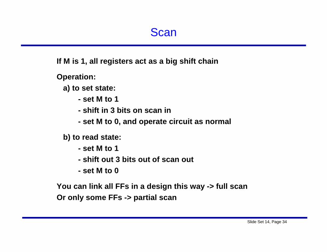
If M is 1, all registers act as a big shift chain
Operation:a) to set state:
- set M to 1- shift in 3 bits on scan in- set M to 0, and operate circuit as normal
b) to read state:- set M to 1- shift out 3 bits out of scan out- set M to 0
You can link all FFs in a design this way -> full scanOr only some FFs -> partial scan
0 1
0 1
0 1
Combinational circuit
z 1
z k
w 1
w n
y 3
y 2
y 1
Y 3
Y 2
Y 1
Clock Scan-in Normal Scan⁄
Scan-out
D Q
D Q
D Q
Slide Set 14, Page 36
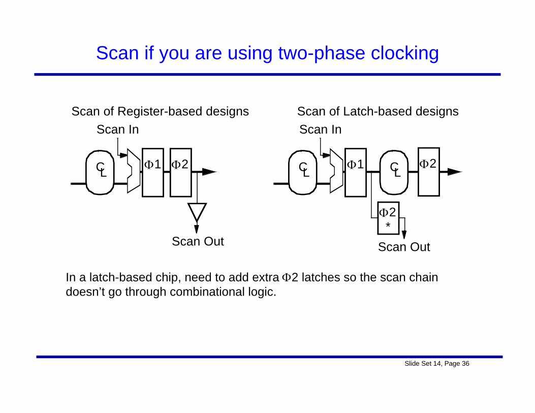
Scan if you are using two-phase clocking
In a latch-based chip, need to add extra Φ2 latches so the scan chain doesn’t go through combinational logic.
Scan of Register-based designs Scan of Latch-based designs
CL Φ1 Φ2
Scan In
Scan Out
CL Φ1
Φ2
Scan In
Scan Out
Φ2CL
*

Slide Set 14, Page 37
Design for LSSD
Does not affect user-visible architecture but
• Makes registers or latches more complex (larger and slightly slower)
→ area penalty.
• The additional wiring taken up by the scan wires is usually minuscule, but this is only true when the CAD flow can generate a good scanordering, which must be determined after cell placement (and then backannotated into logic netlist).
For many semi-custom design, full-scan makes sense since it allows the production test vectors to be generated with good test coverage.
Slide Set 14, Page 38
Built-In-Self-Test
The buzzword BIST is best used to refer to the portions of a design where an additional FSM has been added solely for the purposes of running through a test sequence where the results are NOT observable by the tester on every clock cycle.
Typically, BIST is added to test large (RAM) arrays where the number of clock cycles required by conventional vector-based tests would be just too excessive.
Additionally, BIST can be used to test the delay performance of circuits which would also not be accessible by a tester applying vectors slowly.
The result of BIST is meant to be a pass/fail result, not diagnostic information. Typically, the BIST controller compresses the results into a “signature” which can be compared against the signature of a known good chip.
Unlike other methods of design for testability, adding BIST usually doesn’t really help in providing any controllability for design debug.
Slide Set 14, Page 39
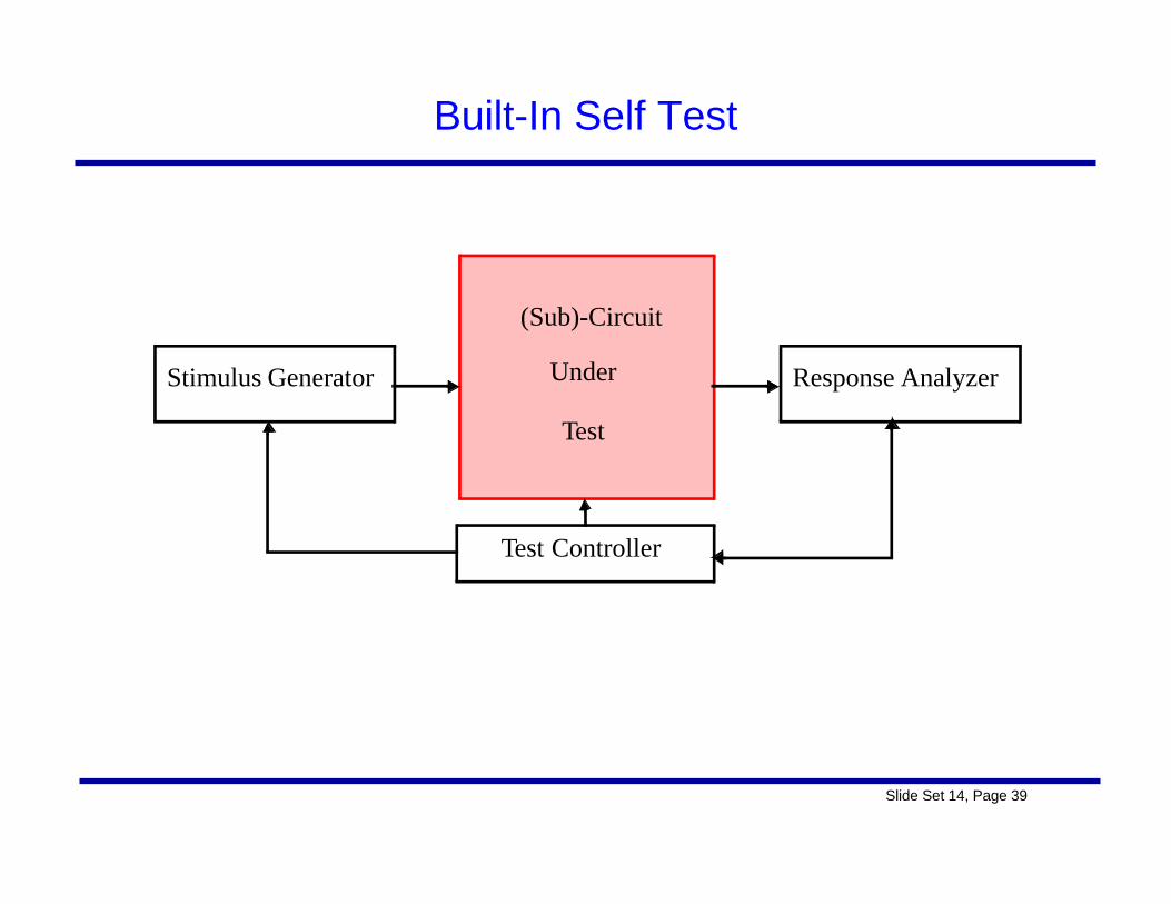
Built-In Self Test
(Sub)-Circuit
Under
Test
Stimulus Generator Response Analyzer
Test Controller
Slide Set 14, Page 40
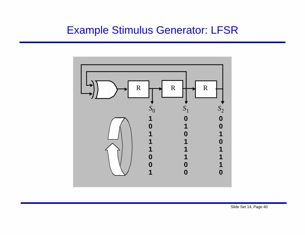
Example Stimulus Generator: LFSR
S0 S1 S2
R R R
1 0 00 1 01 0 11 1 01 1 10 1 10 0 11 0 0
Slide Set 14, Page 41
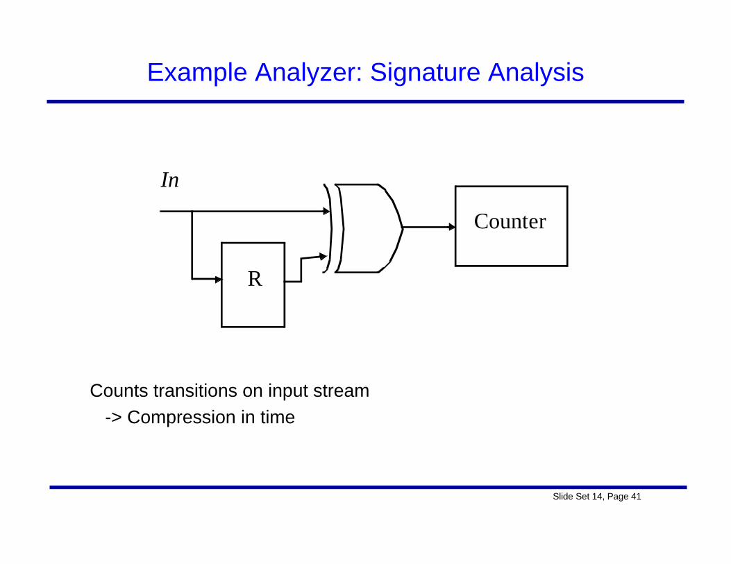
Example Analyzer: Signature Analysis
Counts transitions on input stream-> Compression in time
R
Counter
In
Slide Set 14, Page 42
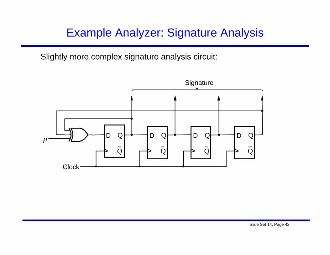
Example Analyzer: Signature Analysis
Slightly more complex signature analysis circuit:
p
Clock
Signature
D Q
Q
D Q
Q
D Q
Q
D Q
Q
Slide Set 14, Page 43
IDDQ Testing
Measuring the quiescent power supply current (IDDQ) as a method of testing is another good idea in CMOS circuits.
Once pure fully-complementary static CMOS circuits have driven their outputs they only draw picoamps from the power supply (leakage)
So, design the chip with a way of turning off all DC power consumption (like ratioed-logic NOR gates), and then after every vector, the power supply current will settle down. Even on big chips with millions of transistors, the leakage current of all the transistors together is less than (or about the order of) the on-current of a single transistor that is stuck on.
So, measuring IDDQ is a great way to detect shorts which will cause fighting output drivers to consume current.
But, don’t have time to measure IDDQ after every test vector, so just measure it after a few well chosen ones, and hope.
With higher leakage currents in recent technologies, this may be more difficult.

Debug

Slide Set 14, Page 45
Silicon Debug
If you find that none of your chips work, then it probably is adesign problem.
Reality: most chips go through a few “spins” before it is correct enough to sell
But, if there is a problem, you have to find the cause FAST
- This is a really stressful time for an engineer
- Better get it right before committing another few million
- What if one bug hides another?

Slide Set 14, Page 46
Silicon Debug
Currently, there is no systematic methodology that Addresses this problem.
There are some ‘hacks’ and point solutions:– controlled un-loading of scan chains=> complicated, careful
clock gating, not full-speed.
– ad-hoc design-specific debug logic => suffers from the “bug prediction” problem.
– external accessible ‘test-points’ => external I/O is expensive and unable to run at internal rates.

Slide Set 14, Page 48
Probing Technology
Micro-probes (nano-probes, pico-probes) are all very thin needles manipulated on a wafer probe station that can get be moved under the microscope and dropped down on specific wires. But often the added capacitance disrupts the circuit so much, that no information is gained about what was happening before the probe changed the circuit.
With an active FET amplifier in the tip, the best micro-probe models can reduce the added capacitance to under 100fF
Voltage levels can be sensed non-mechanically by e-beam testers, which are like sampling digital oscilloscopes that recreate a waveform by repeated sampling at slightly different delay offsets.
Both microprobing and e-beam probing can usually only get to the top layer of metal. Sometimes it is possible to scrape insulation away, to get to the next lower level of metal if it isn’t covered by the top layer. Sometimes laser or ion beam drilling can be used too.
Slide Set 14, Page 49
Single-Die Repair Technology
When a problem is discovered, and a correction proposed, it is desirable to check the correction quicker than waiting many weeks for the re-fabrication cycle.
It is possible to make changes to individual dies by using focused ion-beam (FIB) machines. Together with laser cutting, this allows the capability to both remove and deposit wires. But the wires are much lower quality (hundreds of ohm/square), and deposition rates are slow (on the order of a minute per 100 microns).
Much better to get the chips right in the first place!
Slide Set 14, Page 50
Overall System Test Strategy
To enhance controllability and observability both inside of chipsand at the board level, use the techniques discussed in this lecture:
• Add reset signals and muxes to allow more direct control.• Bring key signals out from inside of complex combinational logic
blocks.• Add Scan to latches/registers.• Add BIST around RAMs or other arrays, using signature
compression to compare the results.