Embed Size (px)
Citation preview
1
2
3
4
5
6
7
8
9
10
20
19
18
17
16
15
14
13
12
11
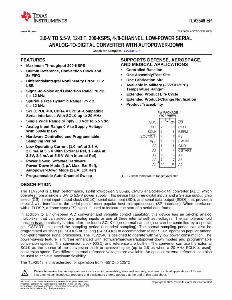
SDO
SDI
SCLK
EOC/(INT)
VCC
A0
A1
A2
A3
A4
CS
REFP
REFM
FS
PWDN
GND
CSTART
A7
A6
A5
PW PACKAGE(TOP VIEW)
TLV2548-EP
www.ti.com SLAS668 –OCTOBER 2009
3.0-V TO 5.5-V, 12-BIT, 200-KSPS, 4-/8-CHANNEL, LOW-POWER SERIALANALOG-TO-DIGITAL CONVERTER WITH AUTOPOWER-DOWN
Check for Samples: TLV2548-EP
1FEATURES SUPPORTS DEFENSE, AEROSPACE,AND MEDICAL APPLICATIONS• Maximum Throughput 200-KSPS• Controlled Baseline• Built-In Reference, Conversion Clock and• One Assembly/Test Site8x FIFO• One Fabrication Site• Differential/Integral Nonlinearity Error: ±1.2• Available in Military (–55°C/125°C)LSB
Temperature Range (1)• Signal-to-Noise and Distortion Ratio: 70 dB,
• Extended Product Life Cyclefi = 12 kHz• Extended Product-Change Notification• Spurious Free Dynamic Range: 75 dB,• Product Traceabilityfi = 12 kHz
• SPI (CPOL = 0, CPHA = 0)/DSP-CompatibleSerial Interfaces With SCLK up to 20 MHz
• Single Wide Range Supply 3.0 Vdc to 5.5 Vdc• Analog Input Range 0 V to Supply Voltage
With 500-kHz BW• Hardware Controlled and Programmable
Sampling Period• Low Operating Current (1.0 mA at 3.3 V,
2.0 mA at 5.5 V With External Ref, 1.7-mA at3.3V, 2.4-mA at 5.5-V With Internal Ref)
• Power Down: Software/HardwarePower-Down Mode (1 μA Max, Ext Ref),Autopower-Down Mode (1 μA, Ext Ref)
• Programmable Auto-Channel Sweep (1) Custom temperature ranges available
DESCRIPTIONThe TLV2548 is a high performance, 12-bit low-power, 3.86-μs, CMOS analog-to-digital converter (ADC) whichoperates from a single 3.0-V to 5.5-V power supply. This device has three digital inputs and a 3-state output [chipselect (CS), serial input-output clock (SCLK), serial data input (SDI), and serial data output (SDO)] that provide adirect 4-wire interface to the serial port of most popular host microprocessors (SPI interface). When interfacedwith a TI DSP, a frame sync (FS) signal is used to indicate the start of a serial data frame.
In addition to a high-speed A/D converter and versatile control capability, this device has an on-chip analogmultiplexer that can select any analog inputs or one of three internal self-test voltages. The sample-and-holdfunction is automatically started after the fourth SCLK edge (normal sampling) or can be controlled by a specialpin, CSTART, to extend the sampling period (extended sampling). The normal sampling period can also beprogrammed as short (12 SCLKs) or as long (24 SCLKs) to accommodate faster SCLK operation popular amonghigh-performance signal processors. The TLV2548 is designed to operate with very low power consumption. Thepower-saving feature is further enhanced with software/hardware/autopower-down modes and programmableconversion speeds. The conversion clock (OSC) and reference are built-in. The converter can use the externalSCLK as the source of the conversion clock to achieve higher (up to 2.8 μs when a 20-MHz SCLK is used)conversion speed. Two different internal reference voltages are available. An optional external reference can alsobe used to achieve maximum flexibility.
The TLV2548 is characterized for operation from –55°C to 125°C.1
Please be aware that an important notice concerning availability, standard warranty, and use in critical applications of TexasInstruments semiconductor products and disclaimers thereto appears at the end of this data sheet.
PRODUCTION DATA information is current as of publication date. Copyright © 2009, Texas Instruments IncorporatedProducts conform to specifications per the terms of the TexasInstruments standard warranty. Production processing does notnecessarily include testing of all parameters.

Command
Decode
SDI
CS
FS EOC/(INT)
Low Power
12-BIT
SAR ADC
Control Logic
CSTART
PWDN
VCC
GND
REFP
An
alo
gM
UX
4/2 V
Reference
S/H
OSC
Conversion
ClockMUX
FIFO
12 Bit × 8
CFR
SCLK
SDO
A0
A1
A2
A3
A4
A5
A6
A7
REFM
CMR (4 MSBs)
INT
EXT
DIV
TLV2548-EP
SLAS668 –OCTOBER 2009 www.ti.com
FUNCTIONAL BLOCK DIAGRAM
Table 1. ORDERING INFORMATION (1)
ORDERABLE PART TOP-SIDE MARKINGTA PACKAGE (2)NUMBER
–55°C to 125°C TSSOP-PW Tape and Reel of 2000 TLV2548MPWREP TV2548EP
(1) For the most current package and ordering information, see the Package Option Addendum at the end of this document, or see the TIWeb site at www.ti.com.
(2) Package drawings, standard packing quantities, thermal data, symbolization, and PCB design guidelines are available atwww.ti.com/sc/package.
Table 2. TERMINAL FUNCTIONS
TERMINALI/O DESCRIPTION
NAME NO.
A0 6A1 7 Analog signal inputs. The analog inputs are applied to these terminals and are internallyA2 8 multiplexed. The driving source impedance should be less than or equal to 1 kΩ.A3 9 xxxIA4 10 For a source impedance greater than 1 kΩ, use the asynchronous conversion start signalA5 11 CSTART (CSTART low time controls the sampling period) or program long sampling periodA6 12 to increase the sampling time.A7 13
Chip select. A high-to-low transition on the CS input resets the internal 4-bit counter,enables SDI, and removes SDO from 3-state within a maximum setup time. SDI is disabledwithin a setup time after the 4-bit counter counts to 16 (clock edges) or a low-to-highCS 20 I transition of CS whichever happens first.NOTE: CS falling and rising edges need to happen when SCLK is low for a microprocessorinterface such as SPI.
2 Submit Documentation Feedback Copyright © 2009, Texas Instruments Incorporated
Product Folder Link(s): TLV2548-EP

TLV2548-EP
www.ti.com SLAS668 –OCTOBER 2009
Table 2. TERMINAL FUNCTIONS (continued)
TERMINALI/O DESCRIPTION
NAME NO.
This terminal controls the start of sampling of the analog input from a selected multiplexchannel. Sampling time starts with the falling edge of CSTART and ends with the rising edgeof CSTART as long as CS is held high. In mode 01, select cycle, CSTART can be issued asCSTART 14 I soon as CHANNEL is selected which means the fifth SCLK during the select cycle, but theeffective sampling time is not started until CS goes to high. The rising edge of CSTART(when CS = 1) also starts the conversion. Tie this terminal to VCC if not used.
End of conversion or interrupt to host processor. [PROGRAMMED AS EOC]: This outputgoes from a high-to-low logic level at the end of the sampling period and remains low untilthe conversion is complete and data are ready for transfer. EOC is used in conversion mode00 only.EOC/(INT) 4 O xxx[PROGRAMMED AS INT]: This pin can also be programmed as an interrupt output signal tothe host processor. The falling edge of INT indicates data are ready for output. The followingCS↓ or FS clears INT.
DSP frame sync input. Indication of the start of a serial data frame in or out of the device. IfFS remains low after the falling edge of CS, SDI is not enabled until an active FS ispresented. A high-to-low transition on the FS input resets the internal 4-bit counter and
FS 17 I enables SDI within a maximum setup time. SDI is disabled within a setup time after the 4-bitcounter counts to 16 (clock edges) or a low-to-high transition of CS whichever happens first.xxxTie this terminal to VCC if not used. See the Data Code Information section, item 1.
Ground return for the internal circuitry. Unless otherwise noted, all voltage measurementsGND 15 I are with respect to GND.
Both analog and reference circuits are powered down when this pin is at logic zero. ThePWDN 16 I device can be restarted by active CS, FS or CSTART after this pin is pulled back to logic
one.
Input serial clock. This terminal receives the serial SCLK from the host processor. SCLK isused to clock the input SDI to the input register. When programmed, it may also be used as
SCLK 3 I the source of the conversion clock.NOTE: This device supports CPOL (clock polarity) = 0, which is SCLK returns to zero whenidling for SPI compatible interface.
Serial data input. The input data is presented with the MSB (D15) first. The first 4-bit MSBs,D(15−12) are decoded as one of the 16 commands. The configure write commands requirean additional 12 bits of data.xxxWhen FS is not used (FS =1), the first MSB (D15) is expected after the falling edge of CSand is latched in on the rising edges of SCLK (after CS↓).SDI 2 I xxxWhen FS is used (typical with an active FS from a DSP) the first MSB (D15) is expectedafter the falling edge of FS and is latched in on the falling edges of SCLK.xxxSDI is disabled within a setup time after the 4-bit counter counts to 16 (clock edges) or alow-to-high transition of CS whichever happens first.
The 3-state serial output for the A/D conversion result. SDO is kept in the high-impedancestate when CS is high and after the CS falling edge and until the MSB is presented. Theoutput format is MSB first.xxxWhen FS is not used (FS = 1 at the falling edge of CS), the MSB is presented to the SDOpin after the CS falling edge, and successive data are available at the rising edge of SCLKand changed on the falling edge.xxx
SDO 1 O When FS is used (FS = 0 at the falling edge of CS), the MSB is presented to SDO after thefalling edge of CS and FS = 0 is detected. Successive data are available at the falling edgeof SCLK and changed on the rising edge. (This is typically used with an active FS from aDSP.)xxxFor conversion and FIFO read cycles, the first 12 bits are result from previous conversion(data) followed by 4 don’t care bits. The first four bits from SDO for CFR read cycles shouldbe ignored. The register content is in the last 12 bits. SDO is 3-state (float) after the 16th bit.See the Data Code Information section, item 2.
External reference input or internal reference decoupling. Tie this pin to analog ground ifREFM 18 I internal reference is used.
Copyright © 2009, Texas Instruments Incorporated Submit Documentation Feedback 3
Product Folder Link(s): TLV2548-EP

Charge
Redistribution
DAC
Control
Logic
_
+
REFM
AinADC Code
TLV2548-EP
SLAS668 –OCTOBER 2009 www.ti.com
Table 2. TERMINAL FUNCTIONS (continued)
TERMINALI/O DESCRIPTION
NAME NO.
External reference input or internal reference decoupling (shunt capacitors of 10 μF and0.1 μF between REFP and REFM). The maximum input voltage range is determined by theREFP 19 I difference between the voltage applied to this terminal and the REFM terminal when anexternal reference is used.
VCC 5 I Positive supply voltage
Detailed Description
Analog Inputs and Internal Test Voltages
The 4/8 analog inputs and three internal test inputs are selected by the analog multiplexer depending on thecommand entered. The input multiplexer is a break-before-make type to reduce input-to-input noise injectionresulting from channel switching.
Converter
The TLV2548 uses a 12-bit successive approximation ADC utilizing a charge redistribution DAC. Figure 1 showsa simplified version of the ADC.
The sampling capacitor acquires the signal on Ain during the sampling period. When the conversion processstarts, the SAR control logic and charge redistribution DAC are used to add and subtract fixed amounts of chargefrom the sampling capacitor to bring the comparator into a balanced condition. When the comparator is balanced,the conversion is complete and the ADC output code is generated.
Figure 1. Simplified Model of the Successive-Approximation System
Serial Interface
INPUT DATA FORMAT
MSB LSB
D15−D12 D11−D0
Command ID[15:12] Configuration data field ID[11:0]
Input data is binary. All trailing blanks can be filled with zeros.
OUTPUT DATA FORMAT READ CFR/FIFO READ
MSB LSB
D15−D12 D11−D0
Don’t care Register content or FIFO content OD[11:0]
4 Submit Documentation Feedback Copyright © 2009, Texas Instruments Incorporated
Product Folder Link(s): TLV2548-EP

TLV2548-EP
www.ti.com SLAS668 –OCTOBER 2009
OUTPUT DATA FORMAT CONVERSION
MSB LSB
D15−D4 D3−D0
Conversion result Don’t careOD[11:0]
The output data format is binary (unipolar straight binary).
Binary
Zero scale code = 000h, Vcode = VREFM.
Full scale code = FFFh, Vcode = VREFP − 1 LSB
Control and Timing
Power Up and Initialization Requirements• Determine processor type by writing A000h to the TLV2548 (CS must be toggled).• Configure the device (CS must make a high-to-low transition, then can be held low if in DSP mode;
i.e., active FS).The first conversion after power up or resuming from power down is not valid.
Start of the Cycle• When FS is not used (FS = 1 at the falling edge of CS), the falling edge of CS is the start of the cycle.• When FS is used (FS is an active signal from a DSP), the falling edge of FS is the start of the cycle.
First 4-MSBs: The Command Register (CMR)
The TLV2548 has a 4-bit command set (see Table 3) plus a 12-bit configuration data field. Most of thecommands require only the first 4 MSBs, i.e., without the 12-bit data field.
The valid commands are listed in Table 3.
Table 3. TLV2548 Command Set (1)
SDI D(15−12) BINARY COMMAND
0000b 0h Select analog input channel 0
0001b 1h Select analog input channel 1
0010b 2h Select analog input channel 2
0011b 3h Select analog input channel 3
0100b 4h Select analog input channel 4
0101b 5h Select analog input channel 5
0110b 6h Select analog input channel 6
0111b 7h Select analog input channel 7
1000b 8h SW power down (analog + reference)
1001b 9h Read CFR register data shown as SDO D(11-0)
Write CFR followed by 12–bit data, e.g., 0A100h means external reference,1010b Ah plus data short sampling, SCLK/4, single shot, INT
1011b Bh Select test, voltage = (REFP+REFM)/2
1100b Ch Select test, voltage = REFM
1101b Dh Select test, voltage = REFP
1110b Eh FIFO read, FIFO contents shown as SDO D(15-4), D(3-0) = 0000
1111b Fh plus data Reserved
(1) The status of the CFR can be read with a read CFR command when the device is programmed for one–shot conversion mode(CFR D[6,5] = 00).
Copyright © 2009, Texas Instruments Incorporated Submit Documentation Feedback 5
Product Folder Link(s): TLV2548-EP

TLV2548-EP
SLAS668 –OCTOBER 2009 www.ti.com
Configuration
Configuration data is stored in one 12–bit configuration register (CFR) (see Table 4 for CFR bit definitions). Onceconfigured after first power up, the information is retained in the H/W or S/W power down state. When the deviceis being configured, a write CFR cycle is issued by the host processor. This is a 16–bit write. If the SCLK stopsafter the first eight bits are entered, then the next eight bits can be taken after the SCLK is resumed.
Table 4. TLV2548 Configuration Register (CFR) Bit Definitions
BIT DEFINITION
Reference selectD11 0: External
1: Internal (Tie REFM to analog ground if the internal reference is selected.)
Internal reference voltage selectD10 0: Internal ref = 4 V
1: internal ref = 2 V
Sample period selectD9 0: Short sampling 12 SCLKs (1x sampling time)
1: Long sampling 24 SCLKs (2x sampling time)
Conversion clock source select00: Conversion clock = internal OSC
D(8,7) 01: Conversion clock = SCLK10: Conversion clock = SCLK/411: Conversion clock = SCLK/2
Conversion mode select00: Single shot mode [FIFO not used, D(1,0) has no effect.]
D(6,5) 01: Repeat mode10: Sweep mode11: Repeat sweep mode
Sweep auto sequence select00: 0-1-2-3-4-5-6-7
D(4,3) (1) 01: 0-2-4-6-0-2-4-610: 0-0-2-2-4-4-6-611: 0-2-0-2-0-2-0-2
EOC/INT - pin function selectD2 0: Pin used as INT
1: Pin used as EOC
FIFO trigger level (sweep sequence length)00: Full (INT generated after FIFO level 7 filled)
D(1,0) 01: 3/4 (INT generated after FIFO level 5 filled)10: 1/2 (INT generated after FIFO level 3 filled)11: 1/4 (INT generated after FIFO level 1 filled)
(1) These bits only take effect in conversion modes 10 and 11.
Sampling
The sampling period starts after the first four input data are shifted in if they are decoded as one of theconversion commands. These are select analog input (channels 0 through 7) and select test (channels 1 through3).
Normal Sampling
When the converter is using normal sampling, the sampling period is programmable. It can be 12 SCLKs (shortsampling) or 24 SCLKs (long sampling). Long sampling helps when SCLK is faster than 10 MHz or when inputsource resistance is high.
Extended Sampling
CSTART - An asynchronous (to the SCLK) signal, via dedicated hardware pin, CSTART, can be used in order tohave total control of the sampling period and the start of a conversion. This extended sampling is user definedand is totally independent of SCLK. While CS is high, the falling edge of CSTART is the start of the samplingperiod and is controlled by the low time of CSTART. The minimum low time for CSTART should be at least equalto the minimum t(SAMPLE). In a select cycle used in mode 01 (REPEAT MODE), CSTART can be started as soon
6 Submit Documentation Feedback Copyright © 2009, Texas Instruments Incorporated
Product Folder Link(s): TLV2548-EP

TLV2548-EP
www.ti.com SLAS668 –OCTOBER 2009
as the channel is selected (after the fifth SCLK). In this case the sampling period is not started until CS hasbecome inactive. Therefore the non-overlapped CSTART low time must meet the minimum sampling timerequirement. The low–to–high transition of CSTART terminates the sampling period and starts the conversionperiod. The conversion clock can also be configured to use either internal OSC or external SCLK. This function isuseful for an application that requires:• The use of an extended sampling period to accommodate different input source impedance.• The use of a faster I/O clock on the serial port but not enough sampling time is available due to the fixed
number of SCLKs. This could be due to a high input source impedance or due to higher MUX ON resistanceat lower supply voltage.
Once the conversion is complete, the processor can initiate a read cycle by using either the read FIFO commandto read the conversion result or by simply selecting the next channel number for conversion. Since the devicehas a valid conversion result in the output buffer, the conversion result is simply presented at the serial dataoutput. To completely get out of the extended sampling mode, CS must be toggled twice from a high-to-lowtransition while CSTART is high. The read cycle mentioned above followed by another configuration cycle of theADC qualifies this condition and successfully puts the ADC back to its normal sampling mode. This can beviewed in Figure 9.
Table 5. Sample and Convert Conditions
CONDITIONS SAMPLE CONVERT
No sampling clock (SCLK) required.Sampling period is totally controlled by the lowtime of CSTART. The high–to–low transitionof CSTART (when CS = 1) starts the sampling
CS = 1 of the analog input signal. The low time ofCSTART (see Figure 11 and CSTART dictates the sampling period. The
Figure 19) low–to–high transition of CSTART endssampling period and begins the conversioncycle. (Note: this trigger only works wheninternal reference is selected for conversionmodes 01, 10, and 11.) 1) If the internal clock OSC is selected, a
maximum conversion time of 3.86 μs can beCSTART = 1 SCLK is required. Sampling period isCS achieved.FS = 1 programmable under normal sampling. When2) If external SCLK is selected, conversionprogrammed to sample under short sampling,time is tconv = 14 x DIV/f(SCLK), where DIV can12 SCLKs are generated to completebe 1, 2, or 4.sampling period. 24 SCLKs are generated
when programmed for long sampling. Acommand set to configure the device requires4 SCLKs thereby extending to 16 or 28
CSTART = 1 SCLKs respectively before conversion takesFS CS = 0 place. (Note: Because the ADC only bypassesa valid channel select command, the user canuse select channel 0, 0000b, as the SDI inputwhen either CS or FS is used as trigger forconversion. The ADC responds to commandssuch as SW powerdown, 1000b.)
TLV2548 Conversion Modes
The TLV2548 has four different conversion modes (mode 00, 01, 10, 11). The operation of each mode is slightlydifferent, depending on how the converter performs the sampling and which host interface is used. The trigger fora conversion can be an active CSTART (extended sampling), CS (normal sampling, SPI interface), or FS (normalsampling, TMS320 DSP interface). When FS is used as the trigger, CS can be held active, i.e. CS does not needto be toggled through the trigger sequence. SDI can be one of the channel select commands, such as SELECTCHANNEL 0. Different types of triggers should not be mixed throughout the repeat and sweep operations. WhenCSTART is used as the trigger, the conversion starts on the rising edge of CSTART. The minimum low time forCSTART is equal to t(SAMPLE). If an active CS or FS is used as the trigger, the conversion is started after the 16thor 28th SCLK edge. Enough time (for conversion) should be allowed between consecutive triggers so that noconversion is terminated prematurely.
One Shot Mode (Mode 00)
One shot mode (mode 00) does not use the FIFO, and the EOC is generated as the conversion is in progress (orINT is generated after the conversion is done).
Copyright © 2009, Texas Instruments Incorporated Submit Documentation Feedback 7
Product Folder Link(s): TLV2548-EP

TLV2548-EP
SLAS668 –OCTOBER 2009 www.ti.com
Repeat Mode (Mode 01)
Repeat mode (mode 01) uses the FIFO. This mode setup requires configuration cycle and channel select cycle.Once the programmed FIFO threshold is reached, the FIFO must be read, or the data is lost when the sequencestarts over again with the SELECT cycle and series of triggers. No configuration is required except forre-selecting the channel unless the operation mode is changed. This allows the host to set up the converter andcontinue monitoring a fixed input and come back to get a set of samples when preferred.
Triggered by CSTART: The first conversion can be started with a select cycle or CSTART. To do so, the usercan issue CSTART during the select cycle, immediately after the 4-bit channel select command. The first samplestarted as soon as the select cycle is finished (i.e., CS returns to 1). If there is enough time (2 μs) left betweenthe SELECT cycle and the following CSTART, a conversion is carried out. In this case, you need one less triggerto fill the FIFO. Succeeding samples are triggered by CSTART.
Sweep Mode (Mode 10)
Sweep mode (mode 10) also uses the FIFO. Once it is programmed in this mode, all of the channels listed in theselected sweep sequence are visited in sequence. The results are converted and stored in the FIFO. This sweepsequence may not be completed if the FIFO threshold is reached before the list is completed. This allows thesystem designer to change the sweep sequence length. Once the FIFO has reached its programmed threshold,an interrupt (INT) is generated. The host must issue a read FIFO command to read and clear the FIFO beforethe next sweep can start.
Repeat Sweep Mode (Mode 11)
Repeat sweep mode (mode 11) works the same way as mode 10 except the operation has an option to continueeven if the FIFO threshold is reached. Once the FIFO has reached its programmed threshold, an interrupt (INT)is generated. Then two things may happen:1. The host may choose to act on it (read the FIFO) or ignore it. If the next cycle is a read FIFO cycle, all of the
data stored in the FIFO is retained until it has been read in order.2. If the next cycle is not a read FIFO cycle, or another CSTART is generated, all of the content stored in the
FIFO is cleared before the next conversion result is stored in the FIFO, and the sweep is continued.
Table 6. TLV2548 Conversion Mode (1) (2) (3)
CONVERSION CFR SAMPLING OPERATIONMODE D(6,5) TYPE
• Single conversion from a selected channel• CS or FS to start select/sampling/conversion/read
Normal • One INT or EOC generated after each conversion• Host must serve INT by selecting channel, and converting and reading the
previous output.
One shot 00 • Single conversion from a selected channel• CS to select/read• CSTART to start sampling and conversionExtended• One INT or EOC generated after each conversion• Host must serve INT by selecting next channel and reading the previous
output.
(1) Programming the EOC/INT pin as the EOC signal works for mode 00 only. The other three modes automatically generate an INT signalirrespective of how EOC/INT is programmed.
(2) Extended sampling mode using CSTART as the trigger only works when internal reference is selected for conversion modes 01, 10, and11.
(3) When using CSTART to sample in extended mode, the falling edge of the next CSTART trigger should occur no more than 2.5 μs afterthe falling CS edge (or falling FS edge if FS is active) of the channel select cycle. This is to prevent an ongoing conversion from beingcanceled.
8 Submit Documentation Feedback Copyright © 2009, Texas Instruments Incorporated
Product Folder Link(s): TLV2548-EP

SCLK
CS
FS
SDI
INT
EOC
SDO
ID14 ID13 ID12 ID15
OD11 OD10 OD9 OD4 OD3
1 2 3 4 7 13 16 112
ID15
14 15
OD2 OD1 OD0
5 6
TLV2548-EP
www.ti.com SLAS668 –OCTOBER 2009
Table 6. TLV2548 Conversion Mode (1) (2) (3) (continued)
CONVERSION CFR SAMPLING OPERATIONMODE D(6,5) TYPE
• Repeated conversions from a selected channel• CS or FS to start sampling/conversion• One INT generated after FIFO is filled up to the threshold
Normal• Host must serve INT by either 1) (FIFO read) reading out all of the FIFO
Repeat 01 contents up to the threshold, then repeat conversions from the same selectedchannel or 2) writing another command(s) to change the conversion mode. Ifthe FIFO is not read when INT is served, it is cleared.
• Same as normal sampling except CSTART starts each sampling andExtendedconversion when CS is high.
• One conversion per channel from a sequence of channels• CS or FS to start sampling/conversion
Normal • One INT generated after FIFO is filled up to the thresholdSweep 10 • Host must serve INT by (FIFO read) reading out all of the FIFO contents up to
the threshold, then write another command(s) to change the conversion mode.
• Same as normal sampling except CSTART starts each sampling andExtendedconversion when CS is high.
• Repeated conversions from a sequence of channels• CS or FS to start sampling/conversion• One INT generated after FIFO is filled up to the threshold
Normal• Host must serve INT by either 1) (FIFO read) reading out all of the FIFO
Repeat sweep 11 contents up to the threshold, then repeat conversions from the same selectedchannel or 2) writing another command(s) to change the conversion mode. Ifthe FIFO is not read when INT is served it is cleared.
• Same as normal sampling except CSTART starts each sampling andExtendedconversion when CS is high.
Timing Diagrams
The timing diagrams can be categorized into two major groups: non-conversion and conversion. Thenon-conversion cycles are read and write (configuration). None of these cycles carry a conversion. Conversioncycles are those four modes of conversion.
Read Cycle (Read FIFO or Read CFR)
Read CFR Cycle
The read command is decoded in the first four clocks. SDO outputs the contents of the CFR after the fourthSCLK. This command works only when the device is programmed in the single shot mode (mode 00).
Figure 2. TLV2548 Read CFR Cycle (FS active)
Copyright © 2009, Texas Instruments Incorporated Submit Documentation Feedback 9
Product Folder Link(s): TLV2548-EP

SCLK
CS
FS
SDI
INT
EOC
SDO
ID14
OD11 OD10 OD9
ID15
1 2 3 4 7 13 16 112 14 155 6
ID14 ID13 ID12ID15
OD4 OD3 OD2 OD1 OD0
SCLK
CS
FS
SDI
INT
EOC
SDO
ID15 ID14 ID13 ID12
OD7 OD5
1 2 3 12
OD11 OD10 OD9 OD6OD8
ID15
OD10OD11
ID14
These devices can perform continuous FIFO read cycles (FS = 1) controlled by SCLK; SCLK can stop between each 16 SCLKs.
4 5 6 7 13 14 15 16 1 2
OD0
TLV2548-EP
SLAS668 –OCTOBER 2009 www.ti.com
Figure 3. TLV2548 Read CFR Cycle (FS = 1)
FIFO Read Cycle
The first command in the active cycle after INT is generated, if the FIFO is used, is assumed as the FIFO readcommand. The first FIFO content is output immediately before the command is decoded. If this command is nota FIFO read, then the output is terminated but the first data in the FIFO is retained until a valid FIFO readcommand is decoded. Use of more layers of the FIFO reduces the time taken to read multiple data. This isbecause the read cycle does not generate EOC or INT, nor does it carry out any conversion.
Figure 4. TLV2548 FIFO Read Cycle (FS = 1)
10 Submit Documentation Feedback Copyright © 2009, Texas Instruments Incorporated
Product Folder Link(s): TLV2548-EP

SCLK
CS
FS
SDI
INT
EOC
SDO
ID14 ID13 ID12 ID15ID11 ID10
1 2 3 16 112
ID15
7 13 14 154 5 6
ID4 ID3 ID2 ID1 ID0ID9
SCLK
CS
FS
SDI
INT
EOC
SDO
ID15 ID14 ID13 ID12 ID15ID11 ID10
1 2 3 16 112
ID14
4 5 6 7 13 1514
ID9 ID4 ID3 ID2 ID1 ID0
TLV2548-EP
www.ti.com SLAS668 –OCTOBER 2009
Write Cycle (Write CFR)
The write cycle is used to write to the configuration register CFR (with 12-bit register content). The write cycledoes not generate an EOC or INT, nor does it carry out any conversion (see power up and initializationrequirements).
Figure 5. TLV2548 Write Cycle (FS Active)
Figure 6. TLV2548 Write Cycle (FS = 1)
Copyright © 2009, Texas Instruments Incorporated Submit Documentation Feedback 11
Product Folder Link(s): TLV2548-EP

SCLK
CS
FS
SDI
INT
EOC
SDO
ID15 ID14I ID13 ID12
1 2 3 4 5 7
(SDOZ on SCLK16L Regardless
of Sampling Time)
t(sample) (12 or 24 SCLKs)
6
ID15
t(conv)
MSB MSB-1 MSB-2 MSB-3 MSB-4 MSB-5 MSB-6 LSB
tc (30 or 42 SCLKs)
16 Short Sampling
28 Long Sampling
30 Short Sampling
42 Long Sampling
MSB
12
(If CONVCLK = SCLK0
SCLK
CS
FS
SDI
INT
EOC
SDO
ID15 ID14 ID13 ID12
1 2 3 4 5 7
(SDOZ on SCLK16L Regardless
of Sampling Time)
t(sample) (12 or 24 SCLKs)
6
ID15
t(conv)
MSB MSB-1 MSB-2 MSB-3 MSB-4 MSB-5 MSB-6 LSB
tc (30 or 42 SCLKs)
16 Short Sampling
28 Long Sampling
30 Short Sampling
42 Long Sampling
MSB
112 13
(If CONVCLK = SCLK0
TLV2548-EP
SLAS668 –OCTOBER 2009 www.ti.com
Conversion Cycles
DSP/Normal Sampling
Figure 7. Mode 00 Single Shot/Normal Sampling (FS Signal Used)
Figure 8. Mode 00 Single Shot/Normal Sampling (FS = 1, FS Signal Not Used)
12 Submit Documentation Feedback Copyright © 2009, Texas Instruments Incorporated
Product Folder Link(s): TLV2548-EP

CS
CSTART
SDI
INT
EOC
SDOHi-Z
Select/Read
Cycle
Select/Read
Cycle
t(sample )
t(conv)
†
Previous Conversion
ResultPrevious Conversion
Result
FS
Hi-Z Hi-Z
Device Going Into
Extended Sampling Mode
Device Get Out
Extended Sampling
ModeRead
Cycle
†
Normal
Cycle
† This is one of the single shot commands. Conversion starts on next rising edge of CSTART.
CS
CSTART
SDI
INT
SDOHi-Z
From Channel 2
FS
† § ‡ ‡ ‡ ‡ §
Hi-Z
Configure SelectConversion #1
SelectConversion #4
Read FIFO #1 #2 #3 #4
Top of FIFO
From Channel 2
¶ ¶ ¶ ¶
† Command = Configure write for mode 01, FIFO threshold = 1/2‡ Command = Read FIFO, first FIFO read§ Command = Select ch2.¶ Use any channel select command to trigger SDI input.
TLV2548-EP
www.ti.com SLAS668 –OCTOBER 2009
Figure 9. Mode 00 Single Shot/Extended Sampling (FS Signal Used, FS Pin Connected to TMS320 DSP)
Modes Using the FIFO: Modes 01, 10, 11 Timing
Figure 10. TLV2548 Mode 01 DSP Serial Interface (Conversions Triggered by FS)
Copyright © 2009, Texas Instruments Incorporated Submit Documentation Feedback 13
Product Folder Link(s): TLV2548-EP

CS
CSTART
SDI
INT
SDOHi-Z
FS
(DSP)
Configure Select
Conversion #1 From Channel 2
Select
Conversion #4 From Channel 2
Read FIFO
First FIFO Read
‡ ‡ ‡ ‡ §
#1 #2 #3 #4
† §
t(sample)
Hi-Z
Sample Times ≥ MIN t(sample)(See Operating Characteristics)
t(sample)
t(sample)
t(sample)
¶
† Command = Configure write for mode 01, FIFO threshold = 1/2‡ Command = Read FIFO, first FIFO read§ Command = Select ch2.¶ Minimum CS low time for select cycle is 6 SCLKs. The same amount of time is required between FS low to CSTART for proper channel decoding.
The low time of CSTART, not overlapped with CS low time, is the valid sampling time for the select cycle (see Figure 19).
CS
CSTART
SDI
INT
SDO
From Channel 0
FS
(DSP)
From Channel 3Configure
Conversion Conversion
Read FIFO #1 #2 #3 #4
Top of FIFO
‡ ‡† ‡ ‡ ‡
Read FIFO #1
From Channel 0
Conversion From Channel 3
Conversion
Repeat
Second FIFO Read
Repeat
First FIFO Read
§ § § § § § § §
† Command = Configure write for mode 10 or 11, FIFO threshold = 1/2, sweep seq = 0-1-2-3.‡ Command = Read FIFO§ Use any channel select command to trigger SDI input.
TLV2548-EP
SLAS668 –OCTOBER 2009 www.ti.com
Figure 11. TLV2548 Mode 01 μp/DSP Serial Interface (Conversions Triggered by CSTART)
Figure 12. TLV2548 Mode 10/11 DSP Serial Interface (Conversions Triggered by FS)
14 Submit Documentation Feedback Copyright © 2009, Texas Instruments Incorporated
Product Folder Link(s): TLV2548-EP

CS
CSTART
SDI
INT
SDO
From Channel 0
FS
(DSP)
Configure
Conversion
Read FIFO #1 #2 #3 #4
Top of FIFO
Read FIFO #1
From Channel 0
Conversion
Repeat
First FIFO Read
Second FIFO ReadRepeat
‡ ‡† ‡ ‡ ‡
From Channel 3
Conversion Conversion
From Channel 3
t(sample)
t(sample)t(sample)
t(sample)
† Command = Configure write for mode 10 or 11, FIFO threshold = 1/2, sweep seq = 0-1-2-3.‡ Command = Read FIFO
CS
CSTART
SDI
INT
SDO
From Channel 0Configure
Conversion Conversion
Read FIFO #1 #2 #3 #4
Top of FIFO
#1
Conversion Conversion
Repeat
First FIFO Read Second FIFO Read
Repeat
‡ ‡† ‡ ‡ ‡
From Channel 3 From Channel 0 From Channel 3
Read FIFO
§ § § § § §§
† Command = Configure write for mode 10 or 11, FIFO threshold = 1/2, sweep seq = 0-1-2-3.‡ Command = Read FIFO§ Use any channel select command to trigger SDI input.
§
TLV2548-EP
www.ti.com SLAS668 –OCTOBER 2009
Figure 13. TLV2548 Mode 10/11 DSP Serial Interface (Conversions Triggered by CSTART)
Figure 14. TLV2548 Mode 10/11 μp Serial Interface (Conversions Triggered by CS)
Copyright © 2009, Texas Instruments Incorporated Submit Documentation Feedback 15
Product Folder Link(s): TLV2548-EP

7 6 5 4 3 2 1 0ADC
12-BITx8
FIFO
SDO
Serial
FIFO Full
FIFO 3/4 Full
FIFO 1/2 Full
FIFO 1/4 Full
FIFO Threshold Pointer
TLV2548-EP
SLAS668 –OCTOBER 2009 www.ti.com
FIFO Operation
Figure 15. TLV2548 FIFO
The device has an eight-layer FIFO that can be programmed for different thresholds. An interrupt is sent to thehost after the pre-programmed threshold is reached. The FIFO can be used to store data from either a fixedchannel or a series of channels based on a pre-programmed sweep sequence. For example, an application mayrequire eight measurements from channel 3. In this case, the FIFO is filled with eight data sequentially takenfrom channel 3. Another application may require data from channel 0, channel 2, channel 4, and channel 6 in anorderly manner. Therefore, the threshold is set for 1/2 and the sweep sequence 0−2−4−6−0−2−4−6 is chosen.An interrupt is sent to the host as soon as all four data are in the FIFO.
In single shot mode, the FIFO automatically uses a 1/8 FIFO depth. Therefore the CFR bits (D1,0) controllingFIFO depth are don’t care.
SCLK and Conversion Speed
There are two ways to adjust the conversion speed.• The SCLK can be used as the source of the conversion clock to get the highest throughput of the device.
The minimum onboard OSC is 3.6 MHz and 14 conversion clocks are required to complete a conversion(corresponding 3.86-μs conversion time). The devices can operate with an SCLK up to 20 MHz for the supplyvoltage range specified. When a more accurate conversion time is desired, the SCLK can be used as thesource of the conversion clock. The clock divider provides speed options appropriate for an application wherea high speed SCLK is used for faster I/O. The total conversion time is 14 x (DIV/fSCLK) where DIV is 1, 2, or 4.For example a 20-MHz SCLK with the divide by 4 option produces a 14 x (4/20 M) = 2.8-μs conversion time.When an external serial clock (SCLK) is used as the source of the conversion clock, the maximum equivalentconversion clock (fSCLK/DIV) should not exceed 6 MHz.
• Autopower down can be used to slow down the device at a reduced power consumption level. This mode isalways used by the converter. If the device is not accessed (by CS or CSTART), the converter is powereddown to save power. The built-in reference is left on in order to quickly resume operation within one halfSCLK period. This provides unlimited choices to trade speed with power savings.
Reference Voltage
The device has a built-in reference with a programmable level of 2 V or 4 V. If the internal reference is used,REFP is set to 2 V or 4 V and REFM should be connected to the analog ground of the converter. An externalreference can also be used through two reference input pins, REFP and REFM, if the reference source isprogrammed as external. The voltage levels applied to these pins establish the upper and lower limits of theanalog inputs to produce a full-scale and zero-scale reading respectively. The values of REFP, REFM, and theanalog input should not exceed the positive supply or be lower than GND consistent with the specified absolutemaximum ratings. The digital output is at full scale when the input signal is equal to or higher than REFP and atzero when the input signal is equal to or lower than REFM.
16 Submit Documentation Feedback Copyright © 2009, Texas Instruments Incorporated
Product Folder Link(s): TLV2548-EP

INTERNAL
REF
Close = Int Ref Used
Open = Ext Ref Used
REFM (See Note 1)
Sample Convert
~50 pF
CDAC
External to the Device
10-mF
Internal
Reference
Compensation
Cap
0.1-mFDecoupling
Cap
REFP
TLV2548-EP
www.ti.com SLAS668 –OCTOBER 2009
Reference Block Equivalent Circuit
A. If internal reference is used, tie REFM to analog ground and install a 10-μF (or 4.7-μF) internal referencecompensation capacitor between REFP and REFM to store the charge as shown in the figure above.
B. If external reference is used, the 10-μF (internal reference compensation) capacitor is optional. REFM can beconnected to external REFM or AGND.
C. Internal reference voltage drift, due to temperature variations, is approximately ±10 mV about the nominal 2 V(typically) from –10°C to 100°C. The nominal value also varies approximately ±50 mV across devices.
D. Internal reference leakage during low ON time: Leakage resistance is on the order of 100 MΩ or more. This meansthe time constant is about 1000 s with 10-μF compensation capacitance. Since the REF voltage does not vary much,the reference comes up quickly after resuming from auto power down. At power up and power down the internalreference sees a glitch of about 500 μV when 2-V internal reference is used (1 mV when 4-V internal reference isused). This glitch settles out after about 50 μs.
Figure 16. Reference Block Equivalent Circuit
Power Down
The device has three power-down modes.
Autopower-Down Mode
The device enters the autopower-down state at the end of a conversion.
In autopower-down, the power consumption reduces to about 1 mA when an internal reference is selected. Thebuilt-in reference is still on to allow the device to resume quickly. The resumption is fast enough (within0.5 SCLK) for use between cycles. An active CS, FS, or CSTART resumes the device from power-down state.The power current is 1 μA when an external reference is programmed and SCLK stops.
Hardware/Software Power-Down Mode
Writing 8000h to the device puts the device into a software power-down state, and the entire chip (including thebuilt-in reference) is powered down. For a hardware power down, the dedicated PWDN pin provides another wayto power down the device asynchronously. These two power-down modes power down the entire deviceincluding the built-in reference to save power. The power-down current is reduced to about 1 μA as the SCLK isstopped.
Copyright © 2009, Texas Instruments Incorporated Submit Documentation Feedback 17
Product Folder Link(s): TLV2548-EP

TLV2548-EP
SLAS668 –OCTOBER 2009 www.ti.com
An active CS, FS, or CSTART restores the device. There is no time delay when an external reference isselected. However, if an internal reference is used, it takes about 20 ms to warm up. Deselect PWDN pin toremove the device from the hardware power-down state. This requires about 20 ms to warm up if an internalreference is also selected.
The configuration register is not affected by any of the power-down modes but the sweep operation sequencehas to be started over again. All FIFO contents are cleared by the power-down modes.
ABSOLUTE MAXIMUM RATINGSover operating free-air temperature range (unless otherwise noted) (1)
VALUE UNIT
Supply voltage range, GND to VCC –0.3 to 6.5 V
Analog input voltage range –0.3 to VCC + 0.3 V
Reference input voltage VCC + 0.3 V
Digital input voltage range –0.3 to VCC + 0.3 V
TJ Operating virtual junction temperature range –55 to 150 °C
TA Operating free-air temperature range –55 to 125 °C
Tstg Storage temperature range –65 to 150 °C
Lead temperature 1,6 mm (1/16 inch) from case for 10 seconds 260 °C
(1) Stresses beyond those listed under the absolute maximum ratings may cause permanent damage to the device. These are stressratings only, and functional operation of the device at these or any other conditions beyond those indicated under the recommendedoperating conditions is not implied. Exposure to absolute-maximum-rated conditions for extended periods may affect device reliability.
DISSIPATION RATINGSTA < 25°C DERATING FACTOR TA = 125°CPACKAGE POWER RATING ABOVE TA = 25°C (1) POWER RATING
20 PW 977 mW 7.8 mW/°C 195 mW
(1) This is the inverse of the traditional junction-to-ambient thermal resistance (RθJA). Thermal resistance is not production tested and thevalues given are for informational purposes only.
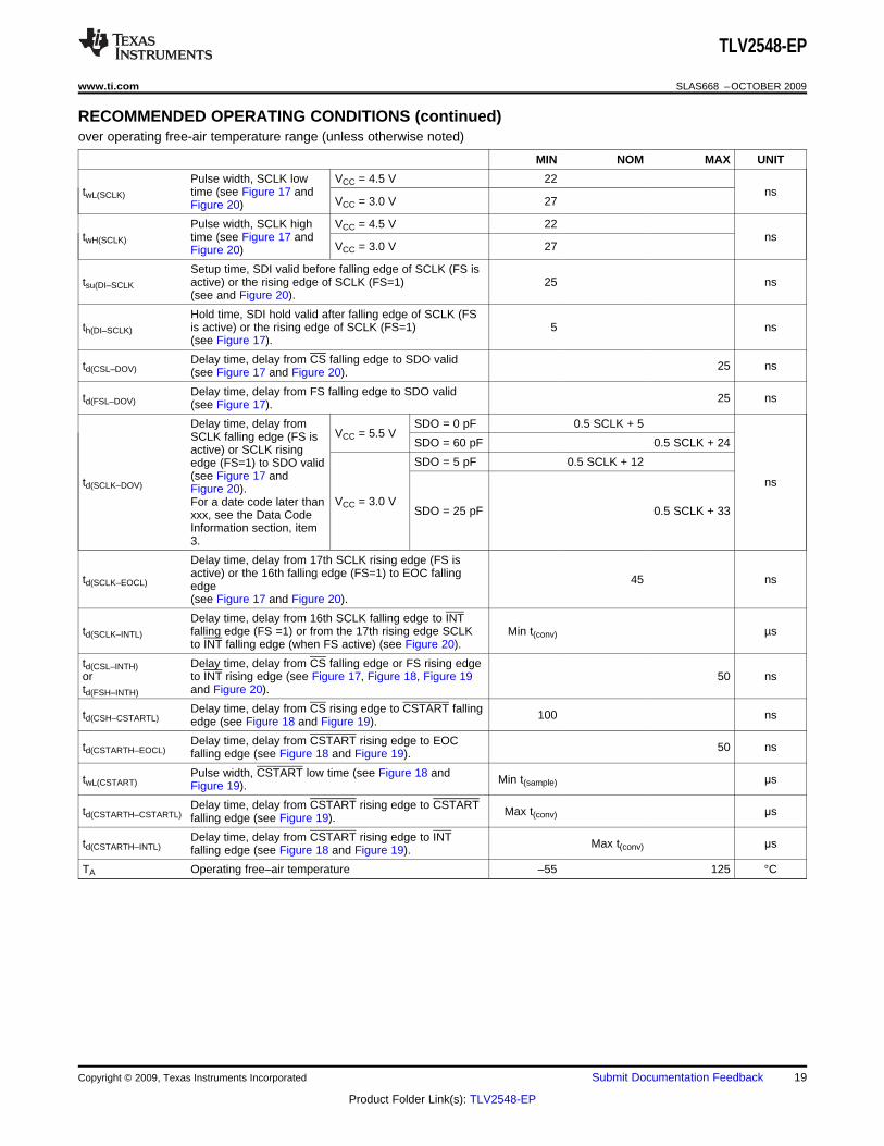
RECOMMENDED OPERATING CONDITIONSover operating free-air temperature range (unless otherwise noted)
MIN NOM MAX UNIT
VCC Supply voltage 3 3.3 5.5 V
Analog input voltage (1) 0 VCC V
VIH High level control input voltage 2.1 V
VIL Low–level control input voltage 0.6 V
Delay time, delay from CS falling edge to FS rising edgetd(CSL–FSH) 0.5 SCLKs(see Figure 17).
Delay time, delay from 16th SCLK falling edge to CStd(SCLK–CSH) rising edge (FS = 1), or 17th rising edge (FS is active) 0.5 SCLKs
(see Figure 17 and Figure 20).
Setup time, FS rising edge before SCLK falling edgetsu(FSH–SCLKL 20 ns(see Figure 17).
Hold time, FS hold high after SCLK falling edgeth(FSH–SCLKL) 30 ns(see Figure 17).
twH(CS) Pulse width, CS high time (see Figure 17 and Figure 20). 100 ns
twH(FS) Pulse width, FS high time (see Figure 17). 0.75 1 SCLKs
SCLK cycle time VCC = 3.0 V to 3.6 V 67 10000tc(SCLK) (see Figure 17 and ns
VCC = 4.5 V to 5.5V 50 10000Figure 20).
(1) When binary output format is used, analog input voltages greater than that applied to REFP convert as all ones (111111111111), whileinput voltages less than that applied to REFM convert as all zeros (000000000000). The device is functional with reference down to 1 V.(VREFP − VREFM − 1); however, the electrical specifications are no longer applicable.
18 Submit Documentation Feedback Copyright © 2009, Texas Instruments Incorporated
Product Folder Link(s): TLV2548-EP
TLV2548-EP
www.ti.com SLAS668 –OCTOBER 2009
RECOMMENDED OPERATING CONDITIONS (continued)over operating free-air temperature range (unless otherwise noted)
MIN NOM MAX UNIT
Pulse width, SCLK low VCC = 4.5 V 22twL(SCLK) time (see Figure 17 and ns
VCC = 3.0 V 27Figure 20)
Pulse width, SCLK high VCC = 4.5 V 22twH(SCLK) time (see Figure 17 and ns
VCC = 3.0 V 27Figure 20)
Setup time, SDI valid before falling edge of SCLK (FS istsu(DI–SCLK active) or the rising edge of SCLK (FS=1) 25 ns
(see and Figure 20).
Hold time, SDI hold valid after falling edge of SCLK (FSth(DI–SCLK) is active) or the rising edge of SCLK (FS=1) 5 ns
(see Figure 17).
Delay time, delay from CS falling edge to SDO validtd(CSL–DOV) 25 ns(see Figure 17 and Figure 20).
Delay time, delay from FS falling edge to SDO validtd(FSL–DOV) 25 ns(see Figure 17).
Delay time, delay from SDO = 0 pF 0.5 SCLK + 5VCC = 5.5 VSCLK falling edge (FS is SDO = 60 pF 0.5 SCLK + 24
active) or SCLK risingSDO = 5 pF 0.5 SCLK + 12edge (FS=1) to SDO valid
(see Figure 17 andtd(SCLK–DOV) nsFigure 20).VCC = 3.0 VFor a date code later than
SDO = 25 pF 0.5 SCLK + 33xxx, see the Data CodeInformation section, item3.
Delay time, delay from 17th SCLK rising edge (FS isactive) or the 16th falling edge (FS=1) to EOC fallingtd(SCLK–EOCL) 45 nsedge(see Figure 17 and Figure 20).
Delay time, delay from 16th SCLK falling edge to INTtd(SCLK–INTL) falling edge (FS =1) or from the 17th rising edge SCLK Min t(conv) µs
to INT falling edge (when FS active) (see Figure 20).
td(CSL–INTH) Delay time, delay from CS falling edge or FS rising edgeor to INT rising edge (see Figure 17, Figure 18, Figure 19 50 nstd(FSH–INTH) and Figure 20).
Delay time, delay from CS rising edge to CSTART fallingtd(CSH–CSTARTL) 100 nsedge (see Figure 18 and Figure 19).
Delay time, delay from CSTART rising edge to EOCtd(CSTARTH–EOCL) 50 nsfalling edge (see Figure 18 and Figure 19).
Pulse width, CSTART low time (see Figure 18 andtwL(CSTART) Min t(sample) μsFigure 19).
Delay time, delay from CSTART rising edge to CSTARTtd(CSTARTH–CSTARTL) Max t(conv) μsfalling edge (see Figure 19).
Delay time, delay from CSTART rising edge to INTtd(CSTARTH–INTL) Max t(conv) μsfalling edge (see Figure 18 and Figure 19).
TA Operating free–air temperature –55 125 °C
Copyright © 2009, Texas Instruments Incorporated Submit Documentation Feedback 19
Product Folder Link(s): TLV2548-EP

TLV2548-EP
SLAS668 –OCTOBER 2009 www.ti.com
ELECTRICAL CHARACTERISTICSover operating free-air temperature range, VCC = VREFP = 3 V to 5.5 V, VREFM = 0 V, SCLK frequency = 20 MHz at 5 V,15 MHz at 3 V (unless otherwise noted)
PARAMETER TEST CONDITIONS MIN TYP (1) MAX UNIT
VCC = 5.5 V, IOH = -0.2 mA at 30 pF load 2.4VOH High–level output voltage V
VCC = 3.0 V, IOH = –20 μA at 30 pF load VCC-0.2
VCC = 5.5 V, IOL = 0.8 mA at 30 pF load 0.4VOL Low–level output voltage V
VCC = 3.0 V, IOL = 20 μA at 30 pF load 0.1
VO = VCC CS = VCC 2.5Off–state output currentIOZ μA(high–impedance–state) VO = 0 CS = VCC –2.5
IIH High–level input current VI = VCC 0.005 2.5 μA
IIL Low–level input current VI = 0 V –0.005 2.5 μA
VCC = 4.5 V to 5.5 V 2CS at 0 V, Ext ref
VCC = 3.0 V to 3.3 V 1Operating supply current,normal short sampling VCC = 4.5 V to 5.5 V 2.4
CS at 0 V, Int refVCC = 3.0 V to 3.3 V 1.7
ICC mAVCC = 4.5 V to 5.5 V 1.1
CS at 0 V, Ext refVCC = 3.0 V to 3.3 V 1Operating supply current,
extended sampling VCC = 4.5 V to 5.5 V 2.1CS at 0 V, Int ref
VCC = 3.0 V to 3.3 V 1.6
Power down supply current VCC = 4.5 V to 5.5 V, Ext clock 1for all digital inputs,ICC(PD) μA0 ≤ VI ≤ 0.3 V or VCC = 2.7 V to 3.3 V, Ext clock 1VI ≥ VCC - 0.3 V, SCLK = 0
Auto power–down current VCC = 4.5 V to 5.5 V, Ext clock, Ext ref 1.0 (2)
for all digital inputs,ICC(AUTOPWDN) μA0 ≤ VI ≤ 0.3 V or VCC = 2.7 V to 3.3 V, Ext ref, Ext clock 1.0 (3)
VI ≥ VCC - 0.3 V, SCLK = 0
Selected channel at VCC 2.5Selected channel leakage μAcurrent Selected channel at 0 V 2.5
Maximum static analogreference current into VREFP = VCC = 5.5 V, VREFM = GND 1 μAREFP (use externalreference)
Analog inputs 45 50Ci Input capacitance pF
Control Inputs 5 25
VCC = 4.5 V 500Zi Input MUX ON resistance Ω
VCC = 2.7 V 600
AC SPECIFICATIONS
Signal-to-noise ratio +SINAD fI = 12 kHz at 200 KSPS 65 71 dBdistortion
TA = –55°C –82 –73THD Total harmonic distortion fI = 12 kHz at 200 KSPS dBAll other –82 –75temperatures
ENOB Effective number of bits fI = 12 kHz at 200 KSPS 11.6 Bits
SFDR Spurious free dynamic range fI = 12 kHz at 200 KSPS –84 –75 dB
Analog Input
Full-power bandwidth, –3 dB 1 MHz
Full-power bandwidth, –1 dB 500 kHz
(1) All typical values are at VCC = 5 V, TA = 25°C.(2) 1.2 mA if internal reference is used, 165 μA if internal clock is used.(3) 0.8 mA if internal reference is used, 116 μA if internal clock is used.
20 Submit Documentation Feedback Copyright © 2009, Texas Instruments Incorporated
Product Folder Link(s): TLV2548-EP

TLV2548-EP
www.ti.com SLAS668 –OCTOBER 2009
ELECTRICAL CHARACTERISTICS (continued)over operating free-air temperature range, VCC = VREFP = 3 V to 5.5 V, VREFM = 0 V, SCLK frequency = 20 MHz at 5 V,15 MHz at 3 V (unless otherwise noted)
PARAMETER TEST CONDITIONS MIN TYP (1) MAX UNIT
REFERENCE SPECIFICATIONS (4)
(0.1 μF and 10 μF between REFP andREFM pins)
Positive reference inputREFP VCC = 2.7 V to 5.5 V 2 VCC Vvoltage
Negative reference inputREFM VCC = 2.7 V to 5.5 V 0 2 Vvoltage
CS = 1, SCLK = 0, (off) 100 MΩVCC = 5.5 V SCLK = 20 MHzCS = 0, 20 25 kΩ(on)
Reference Input impedanceCS = 1, SCLK = 0 (off) 100 MΩ
VCC = 2.7 V SCLK = 15 MHzCS = 0, 20 25 kΩ(on)
Reference Input voltageREFP-REFM VCC = 2.7 V to 5.5 V 2 VCC Vdifference
VCC = 5.5 V VREF SELECT = 4 V 3.85 4 4.15
REFP-REFM Internal reference voltage VCC = 5.5 V VREF SELECT = 2 V 1.925 2 2.075 V
VCC = 2.7 V VREF SELECT = 2 V 1.925 2 2.075
Internal reference start–up VCC = 5.5 V, 2.7 V with 10 μF compensation cap 20 mstime
Internal reference VCC = 2.7 V to 5.5 V 16 40 (5) PPM/°Ctemperature coefficient
(4) Specified by design.(5) Specified by design.
Copyright © 2009, Texas Instruments Incorporated Submit Documentation Feedback 21
Product Folder Link(s): TLV2548-EP
TLV2548-EP
SLAS668 –OCTOBER 2009 www.ti.com
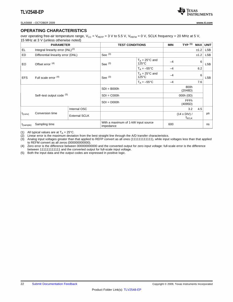
OPERATING CHARACTERISTICSover operating free-air temperature range, VCC = VREFP = 3 V to 5.5 V, VREFM = 0 V, SCLK frequency = 20 MHz at 5 V,15 MHz at 3 V (unless otherwise noted)
PARAMETER TEST CONDITIONS MIN TYP (1) MAX UNIT
EL Integral linearity error (INL) (2) ±1.2 LSB
ED Differential linearity error (DNL) See (3) ±1.2 LSB
TA = 25°C and –4 6125°CEO Offset error (4) See (3) LSBTA = –55°C –4 6.2
TA = 25°C and –4 6125°CEFS Full scale error (4) See (3) LSBTA = –55°C –4 7.6
800hSDI = B000h (2048D)
Self–test output code (5) SDI = C000h 000h (0D)
FFFhSDI = D000h (4095D)
Internal OSC 3.2 4.5t(conv) Conversion time μs(14 x DIV) /External SCLK fSCLK
With a maximum of 1-kW input sourcet(sample) Sampling time 600 nsimpedance
(1) All typical values are at TA = 25°C.(2) Linear error is the maximum deviation from the best straight line through the A/D transfer characteristics.(3) Analog input voltages greater than that applied to REFP convert as all ones (111111111111), while input voltages less than that applied
to REFM convert as all zeros (000000000000).(4) Zero error is the difference between 000000000000 and the converted output for zero input voltage: full-scale error is the difference
between 111111111111 and the converted output for full-scale input voltage.(5) Both the input data and the output codes are expressed in positive logic.
22 Submit Documentation Feedback Copyright © 2009, Texas Instruments Incorporated
Product Folder Link(s): TLV2548-EP

twL(SCLK)
Hi-ZHi-ZVOH
VOL
VIH
VIL
VIH
VIL
VIH
VIL
VOH
VOL
VOH
VOL
SCLK
SDI
SDO
EOC
INT
don’t care
td(SCLK-CSH)
tsu(DI-SCLK)
td(SCLK-EOCL)
td(SCLK-INTL)
tWH(FS)
ID1
don’t careOD10
ID0ID14
161521
ID15
OD11
td(SCLK-DOV)
t(conv)
CS
td(CSL-DOV)
td(FSL-DOV)
td(FSH-INTH)
OD15
td(CSL-FSH)
tsu(FSH-SCLKL)
th(FSH-SCLKL)
twH(CS)
td(FSL-DOV)
tc(SCLK)
twH(SCLK)
td(CSL-INTH)
FS
th(DI-SCLK)
CS
CSTART
EOC
INT
VOH
VOL
VIH
VIL
VOH
VOL
VIH
VIL
td(CSH-CSTARTL)
twL(CSTART)
t(CONV)
td(CSTARTH-EOCL)
td(CSL-INTH)
td(CSTARTH-INTL)
SELECT CYCLE
†
† CSTART falling edge may come before the rising edge of CS but no sooner than the fifth SCLK of the SELECT CYCLE.
TLV2548-EP
www.ti.com SLAS668 –OCTOBER 2009
PARAMETER MEASUREMENT INFORMATION
Figure 17. Critical Timing, DSP Mode (Normal Sampling, FS is Active)
Figure 18. Critical Timing (Extended Sampling, Single Shot)
Copyright © 2009, Texas Instruments Incorporated Submit Documentation Feedback 23
Product Folder Link(s): TLV2548-EP
VIH
VIL
VOH
VOL
VOH
VOL
VIH
VIL
CS
CSTART
EOC
INT
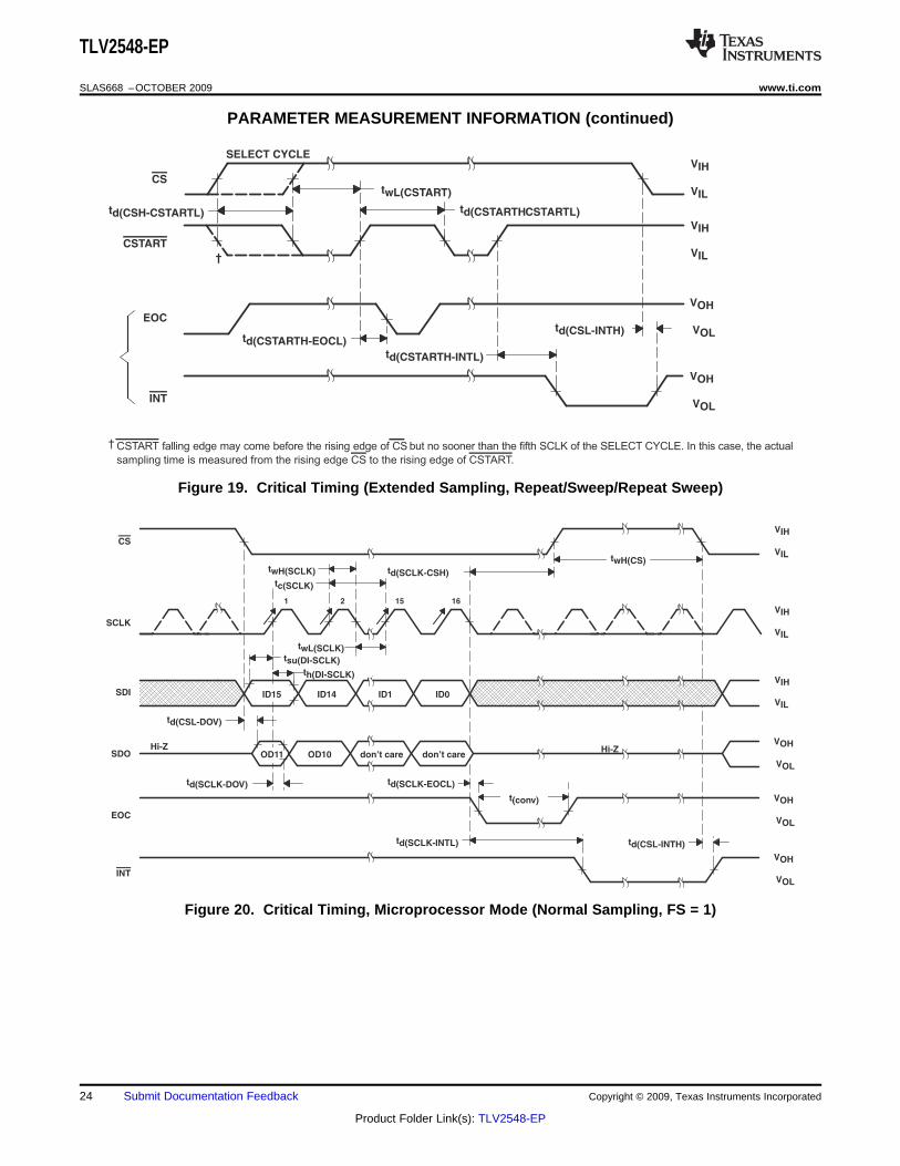
td(CSH-CSTARTL)
twL(CSTART)
td(CSTARTHCSTARTL)
td(CSTARTH-EOCL)
td(CSTARTH-INTL)
td(CSL-INTH)
SELECT CYCLE
†
† CSTART falling edge may come before the rising edge of CS but no sooner than the fifth SCLK of the SELECT CYCLE. In this case, the actual
sampling time is measured from the rising edge CS to the rising edge of CSTART.
Hi-ZHi-ZVOH
VOL
VIH
VIL
VIH
VIL
VIH
VIL
VOH
VOL
VOH
VOL
CS
SCLK
SDI
SDO
EOC
INT
don’t care
twH(CS)
twL(SCLK)
tc(SCLK)
tsu(DI-SCLK)
td(CSL-DOV)
td(SCLK-EOCL)
td(SCLK-INTL) td(CSL-INTH)
twH(SCLK)
ID1
don’t careOD10
ID0ID14
161521
ID15
OD11
td(SCLK-DOV)
t(conv)
td(SCLK-CSH)
th(DI-SCLK)
TLV2548-EP
SLAS668 –OCTOBER 2009 www.ti.com
PARAMETER MEASUREMENT INFORMATION (continued)
Figure 19. Critical Timing (Extended Sampling, Repeat/Sweep/Repeat Sweep)
Figure 20. Critical Timing, Microprocessor Mode (Normal Sampling, FS = 1)
24 Submit Documentation Feedback Copyright © 2009, Texas Instruments Incorporated
Product Folder Link(s): TLV2548-EP

0.5
0.49
0.48
0.47
-40 25
INL
-In
teg
ralN
on
lin
eari
ty-
LS
B
0.51
0.52
90
TA - Temperature - °C
VCC = 2.7 V, Internal Reference = 2 V,
Internal Oscillator, Single Shot,
Short Sample, Mode 00 mP Mode
-23.75 -7.5 41.25 57.5 73.75
0.53
8.75
0.58
0.575
0.565
0.56
0.59
0.595
0.6
0.585
0.57
INL
-In
teg
ralN
on
lin
eari
ty-
LS
B
A - Temperature - °C
VCC = 5.5 V, Internal Reference = 2 V,
Internal Oscillator, Single Shot,
Short Sample, Mode 00 mP Mode
-40 25 90-23.75 -7.5 8.75 41.25 57.5 73.75
T
0.49
0.488
0.48
0.478
DN
L-
Dif
fere
nti
alN
on
lin
eari
ty-
LS
B
0.492
0.494
0.486
0.484
0.482
TA - Temperature - °C
VCC = 2.7 V, Internal Reference = 2 V,
Internal Oscillator, Single Shot,
Short Sample, Mode 00 mP Mode
-40 25 90-23.75 -7.5 8.75 41.25 57.5 73.75
0.496
0.45
0.44
0.43
0.42
0.46
0.47
0.48
DN
L-
Dif
fere
nti
alN
on
lin
eari
ty-
LS
B
A - Temperature - °C
VCC = 5.5 V, Internal Reference = 2 V,
Internal Oscillator, Single Shot,
Short Sample, Mode 00 mP Mode
-40 25 90-23.75 -7.5 8.75 41.25 57.5 73.75
T
TLV2548-EP
www.ti.com SLAS668 –OCTOBER 2009
TYPICAL CHARACTERISTICSINTEGRAL NONLINEARITY INTEGRAL NONLINEARITY
vs vsTEMPERATURE TEMPERATURE
Figure 21. Figure 22.
DIFFERENTIAL NONLINEARITY DIFFERENTIAL NONLINEARITYvs vs
TEMPERATURE TEMPERATURE
Figure 23. Figure 24.
Copyright © 2009, Texas Instruments Incorporated Submit Documentation Feedback 25
Product Folder Link(s): TLV2548-EP

-1
-1.5
-2
-2.5G
ain
Err
or
- L
SB
-0.5
0
TA - Temperature - °C
VCC = 5 V, Internal Reference = 4 V,
External Oscillator = SCLK/4,
Single Shot, Long Sample,
Mode 00 mP Mode
-40 25 90-23.75 -7.5 8.75 41.25 57.5 73.75
0.5
0.6
0.4
0.2
0
Off
set
Err
or
- L
SB 0.8
1
TA - Temperature - °C
VCC = 5 V, Internal Reference = 4 V,
External Oscillator = SCLK/4,
Single Shot, Long Sample,
Mode 00 mP Mode
-40 25 90-23.75 -7.5 8.75 41.25 57.5 73.75
1.2
1
0.8
0.6
Su
pp
ly C
urr
en
t -
mA
1.2
TA - Temperature - °C
Long Sample
Short Sample
VCC = 5 V, External Reference = 4 V,
Internal Oscillator, Single Shot,
Short Sample, Mode 00 mP Mode
-40 25 90-23.75 -7.5 8.75 41.25 57.5 73.75
1.4
0.2
0.6
0.8
1
Po
werd
ow
n C
urr
en
t -
Am
0
0.2
0.4
A - Temperature - °C
VCC = 2.7 V
VCC = 5 V
VCC = 5.5 V
External Reference = 4 V, Internal Oscillator,
Single Shot, Short Sample, Mode 00 mP Mode
-40 25 90-23.75 -7.5 8.75 41.25 57.5 73.75
0.4
T
TLV2548-EP
SLAS668 –OCTOBER 2009 www.ti.com
TYPICAL CHARACTERISTICS (continued)OFFSET ERROR GAIN ERROR
vs vsTEMPERATURE TEMPERATURE
Figure 25. Figure 26.
SUPPLY CURRENT POWER DOWN CURRENTvs vs
TEMPERATURE TEMPERATURE
Figure 27. Figure 28.
26 Submit Documentation Feedback Copyright © 2009, Texas Instruments Incorporated
Product Folder Link(s): TLV2548-EP

-1.0
-0.5
0.0
0.5
1.0
0 4097
INL
-In
teg
ralN
on
lin
eari
ty-
LS
B
Samples
VCC = 2.7 V, Internal Reference = 2 V, Internal Oscillator,
Single Shot, Short Sample, Mode 00 mP Mode
-1.0
-0.5
0.0
0.5
1.0
0 4097DN
L-
Dif
fere
nti
alN
on
lin
eari
ty-
LS
B
Samples
VCC = 2.7 V, Internal Reference = 2 V, Internal Oscillator,
Single Shot, Short Sample, Mode 00 mP Mode
-1.0
-0.5
0.0
0.5
1.0
0 4097
INL
-In
teg
ralN
on
lin
eari
ty-
LS
B
Samples
VCC = 5 V, Internal Reference = 2 V, Internal Oscillator,
Single Shot, Short Sample, Mode 00 mP Mode
TLV2548-EP
www.ti.com SLAS668 –OCTOBER 2009
TYPICAL CHARACTERISTICS (continued)INTEGRAL NONLINEARITY
vsSAMPLES
Figure 29.
DIFFERENTIAL NONLINEARITYvs
SAMPLES
Figure 30.
INTEGRAL NONLINEARITYvs
SAMPLES
Figure 31.
Copyright © 2009, Texas Instruments Incorporated Submit Documentation Feedback 27
Product Folder Link(s): TLV2548-EP

-1.0
-0.5
0.0
0.5
1.0
0 4097DN
L-
Dif
fere
nti
alN
on
lin
eari
ty-
LS
B
Samples
VCC = 5 V, Internal Reference = 2 V, Internal Oscillator,
Single Shot, Short Sample, Mode 00 mP Mode
40
00 10
Mag
nit
ud
e -
dB 110
120
f - Frequency - kHz
100%160150140130
1009080706050
302010
5 15
VCC = 5 V, External Reference = 4 V,
Internal Oscillator , Single Shot, Long Sample, Mode 00 mP
Mode @ 200 KSPS
20 25 30 35 40 45 50 55 60 65 70 75 80 85 90 95 100
TLV2548-EP
SLAS668 –OCTOBER 2009 www.ti.com
TYPICAL CHARACTERISTICS (continued)DIFFERENTIAL NONLINEARITY
vsSAMPLES
Figure 32.
MAGNITUDEvs
FREQUENCY
Figure 33.
28 Submit Documentation Feedback Copyright © 2009, Texas Instruments Incorporated
Product Folder Link(s): TLV2548-EP

-71
-70.50
-70
-69.50
-69
-68.50
-68
-67.50
-67
0
SIN
AD
- S
ign
al-
to-N
ois
e +
Dis
tort
ion
- d
B
f - Frequency - kHz
VCC = 5 V,
External Reference = 4 V,
Internal Oscillator,
Single Shot, Long Sample,
Mode 00 mP Mode
50 100 15010.80
10.90
11
11.10
11.20
11.30
11.40
11.50
0E
NO
B -
Eff
ecti
ve N
um
ber
of
Bit
s -
BIT
S
f - Frequency - kHz
VCC = 5 V,
External Reference = 4 V,
Internal Oscillator,
Single Shot, Long Sample,
Mode 00 mP Mode
50 100 150
-79
-78
-77
-76
-75
-74
-73
-72
-71
-70
-69
0
TH
D-To
talH
arm
on
icD
isto
rtio
n-
dB
f - Frequency - kHz
VCC = 5 V,
External Reference = 4 V,
Internal Oscillator,
Single Shot, Long Sample,
Mode 00 mP Mode
50 100 150-82
-81
-80
-79
-78
-77
-76
-75
-74
-73
0
Sp
uri
ou
s F
ree D
yn
am
ic R
an
ge -
dB
f - Frequency - kHz
VCC = 5 V,
External Reference = 4 V,
Internal Oscillator,
Single Shot, Long Sample,
Mode 00 mP Mode
50 100 150
TLV2548-EP
www.ti.com SLAS668 –OCTOBER 2009
TYPICAL CHARACTERISTICS (continued)SIGNAL-TO-NOISE + DISTORTION EFFECTIVE NUMBER OF BITS
vs vsINPUT FREQUENCY INPUT FREQUENCY
Figure 34. Figure 35.
TOTAL HARMONIC DISTORTION SPURIOUS FREE DYNAMIC RANGEvs vs
INPUT FREQUENCY INPUT FREQUENCY
Figure 36. Figure 37.
Copyright © 2009, Texas Instruments Incorporated Submit Documentation Feedback 29
Product Folder Link(s): TLV2548-EP

-71.4
-71.2
-71
-70.8
-70.6
-70.4
-70.2
0
SN
R -
Sig
nal-
to-N
ois
e R
ati
o -
dB
f - Frequency - kHz
VCC = 5 V,
External Reference = 4 V,
Internal Oscillator,
Single Shot, Long Sample,
Mode 00 mP Mode
50 100 150
GND
CSXF
TMS320 DSP
TLV2548
SDI
SDO
SCLK
INT
TXD
RXD
CLKR
BIO
10 kΩ
vcc
AIN
VDD
FSR
FS
CLKX
FSX
TLV2548-EP
SLAS668 –OCTOBER 2009 www.ti.com
TYPICAL CHARACTERISTICS (continued)SIGNAL-TO-NOISE RATIO
vsINPUT FREQUENCY
Figure 38.
PRINCIPLES OF OPERATION
Figure 39. Typical Interface to a TMS320 DSP
DATA CODE INFORMATION
Parts with a date code earlier than 31xxxxx have the following discrepancies:1. Earlier devices react to FS input irrespective of the state of the CS signal.2. The earlier silicon was designed with SDO prereleased half clock ahead. This means in the microcontroller
mode (FS=1) the SDO is changed on the rising edge of SCLK with a delay; and for DSP serial port (when FSis active) the SDO is changed on the falling edge of SCLK with a delay. This helps the setup time forprocessor input data, but may reduce the hold time for processor input data. It is recommended that a100-pF capacitance be added to the SDO line of the ADC when interfacing with a slower processor that
30 Submit Documentation Feedback Copyright © 2009, Texas Instruments Incorporated
Product Folder Link(s): TLV2548-EP

TLV2548-EP
www.ti.com SLAS668 –OCTOBER 2009
requires longer input data hold time.3. For earlier silicon, the delay time is specified as:
MIN NOM MAX UNIT
SDO = 0 pF 16VCC = 4.5 VDelay time, delay from SCLK falling edge (FS is SDO = 100 pF 20
active) or SDO = 100 pF 20 ns SCLK rising edge nsSDO = 0 pF 24(FS = 1) to next SDO valid, td(SCLK-DOV). VCC = 2.7 V
SDO = 100 pF 30
This is because the SDO is changed at the rising edge in the up mode with a delay. This is the hold timerequired by the external digital host processor, therefore, a minimum value is specified. The newer siliconhas been revised with SDO changed at the falling edge in the up mode with a delay. Since at least 0.5 SCLKexists as the hold time for the external host processor, the specified maximum value helps with thecalculation of the setup time requirement of the external digital host processor.
For an explanation of the DSP mode, reverse the rising/falling edges in item 2. above.
Copyright © 2009, Texas Instruments Incorporated Submit Documentation Feedback 31
Product Folder Link(s): TLV2548-EP
PACKAGE OPTION ADDENDUM
www.ti.com 10-Dec-2020
Addendum-Page 1
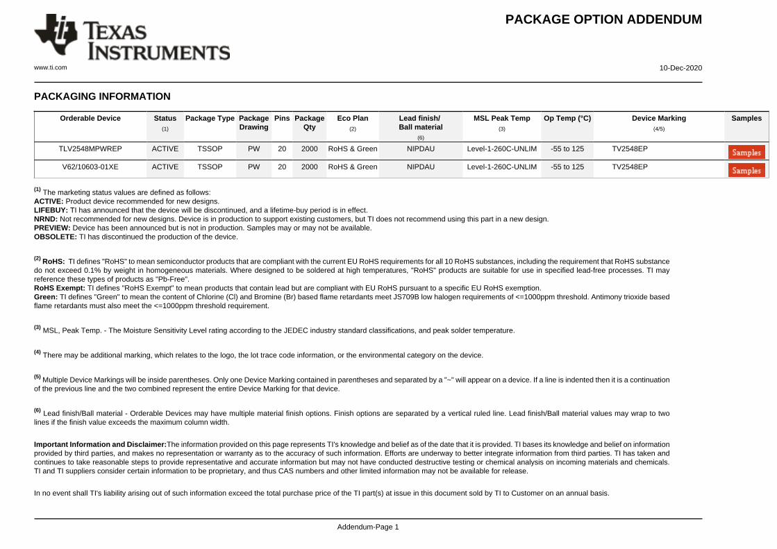
PACKAGING INFORMATION
Orderable Device Status(1)
Package Type PackageDrawing
Pins PackageQty
Eco Plan(2)
Lead finish/Ball material
(6)
MSL Peak Temp(3)
Op Temp (°C) Device Marking(4/5)
Samples
TLV2548MPWREP ACTIVE TSSOP PW 20 2000 RoHS & Green NIPDAU Level-1-260C-UNLIM -55 to 125 TV2548EP
V62/10603-01XE ACTIVE TSSOP PW 20 2000 RoHS & Green NIPDAU Level-1-260C-UNLIM -55 to 125 TV2548EP
(1) The marketing status values are defined as follows:ACTIVE: Product device recommended for new designs.LIFEBUY: TI has announced that the device will be discontinued, and a lifetime-buy period is in effect.NRND: Not recommended for new designs. Device is in production to support existing customers, but TI does not recommend using this part in a new design.PREVIEW: Device has been announced but is not in production. Samples may or may not be available.OBSOLETE: TI has discontinued the production of the device.
(2) RoHS: TI defines "RoHS" to mean semiconductor products that are compliant with the current EU RoHS requirements for all 10 RoHS substances, including the requirement that RoHS substancedo not exceed 0.1% by weight in homogeneous materials. Where designed to be soldered at high temperatures, "RoHS" products are suitable for use in specified lead-free processes. TI mayreference these types of products as "Pb-Free".RoHS Exempt: TI defines "RoHS Exempt" to mean products that contain lead but are compliant with EU RoHS pursuant to a specific EU RoHS exemption.Green: TI defines "Green" to mean the content of Chlorine (Cl) and Bromine (Br) based flame retardants meet JS709B low halogen requirements of <=1000ppm threshold. Antimony trioxide basedflame retardants must also meet the <=1000ppm threshold requirement.
(3) MSL, Peak Temp. - The Moisture Sensitivity Level rating according to the JEDEC industry standard classifications, and peak solder temperature.
(4) There may be additional marking, which relates to the logo, the lot trace code information, or the environmental category on the device.
(5) Multiple Device Markings will be inside parentheses. Only one Device Marking contained in parentheses and separated by a "~" will appear on a device. If a line is indented then it is a continuationof the previous line and the two combined represent the entire Device Marking for that device.
(6) Lead finish/Ball material - Orderable Devices may have multiple material finish options. Finish options are separated by a vertical ruled line. Lead finish/Ball material values may wrap to twolines if the finish value exceeds the maximum column width.
Important Information and Disclaimer:The information provided on this page represents TI's knowledge and belief as of the date that it is provided. TI bases its knowledge and belief on informationprovided by third parties, and makes no representation or warranty as to the accuracy of such information. Efforts are underway to better integrate information from third parties. TI has taken andcontinues to take reasonable steps to provide representative and accurate information but may not have conducted destructive testing or chemical analysis on incoming materials and chemicals.TI and TI suppliers consider certain information to be proprietary, and thus CAS numbers and other limited information may not be available for release.
In no event shall TI's liability arising out of such information exceed the total purchase price of the TI part(s) at issue in this document sold by TI to Customer on an annual basis.

PACKAGE OPTION ADDENDUM
www.ti.com 10-Dec-2020
Addendum-Page 2
OTHER QUALIFIED VERSIONS OF TLV2548-EP :
• Catalog: TLV2548
• Military: TLV2548M
NOTE: Qualified Version Definitions:
• Catalog - TI's standard catalog product
• Military - QML certified for Military and Defense Applications
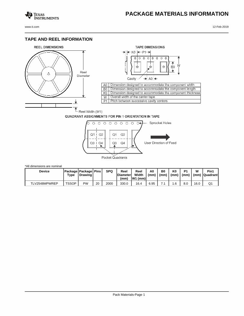
TAPE AND REEL INFORMATION
*All dimensions are nominal
Device PackageType
PackageDrawing
Pins SPQ ReelDiameter
(mm)
ReelWidth
W1 (mm)
A0(mm)
B0(mm)
K0(mm)
P1(mm)
W(mm)
Pin1Quadrant
TLV2548MPWREP TSSOP PW 20 2000 330.0 16.4 6.95 7.1 1.6 8.0 16.0 Q1
PACKAGE MATERIALS INFORMATION
www.ti.com 12-Feb-2019
Pack Materials-Page 1

*All dimensions are nominal
Device Package Type Package Drawing Pins SPQ Length (mm) Width (mm) Height (mm)
TLV2548MPWREP TSSOP PW 20 2000 350.0 350.0 43.0
PACKAGE MATERIALS INFORMATION
www.ti.com 12-Feb-2019
Pack Materials-Page 2

www.ti.com
PACKAGE OUTLINE
C
18X 0.65
2X5.85
20X 0.300.19
TYP6.66.2
1.2 MAX
0.150.05
0.25GAGE PLANE
-80
BNOTE 4
4.54.3
A
NOTE 3
6.66.4
0.750.50
(0.15) TYP
TSSOP - 1.2 mm max heightPW0020ASMALL OUTLINE PACKAGE
4220206/A 02/2017
1
1011
20
0.1 C A B
PIN 1 INDEX AREA
SEE DETAIL A
0.1 C
NOTES: 1. All linear dimensions are in millimeters. Any dimensions in parenthesis are for reference only. Dimensioning and tolerancing per ASME Y14.5M. 2. This drawing is subject to change without notice. 3. This dimension does not include mold flash, protrusions, or gate burrs. Mold flash, protrusions, or gate burrs shall not exceed 0.15 mm per side. 4. This dimension does not include interlead flash. Interlead flash shall not exceed 0.25 mm per side.5. Reference JEDEC registration MO-153.
SEATINGPLANE
A 20DETAIL ATYPICAL
SCALE 2.500
www.ti.com
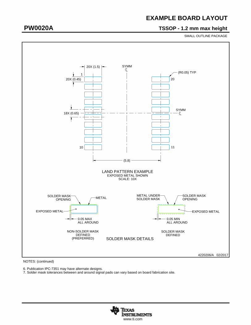
EXAMPLE BOARD LAYOUT
0.05 MAXALL AROUND
0.05 MINALL AROUND
20X (1.5)
20X (0.45)
18X (0.65)
(5.8)
(R0.05) TYP
TSSOP - 1.2 mm max heightPW0020ASMALL OUTLINE PACKAGE
4220206/A 02/2017
NOTES: (continued) 6. Publication IPC-7351 may have alternate designs. 7. Solder mask tolerances between and around signal pads can vary based on board fabrication site.
LAND PATTERN EXAMPLEEXPOSED METAL SHOWN
SCALE: 10X
SYMM
SYMM
1
10 11
20
15.000
METALSOLDER MASKOPENING
METAL UNDERSOLDER MASK
SOLDER MASKOPENING
EXPOSED METALEXPOSED METAL
SOLDER MASK DETAILS
NON-SOLDER MASKDEFINED
(PREFERRED)
SOLDER MASKDEFINED
www.ti.com
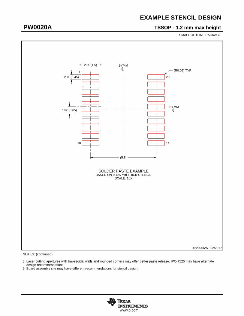
EXAMPLE STENCIL DESIGN
20X (1.5)
20X (0.45)
18X (0.65)
(5.8)
(R0.05) TYP
TSSOP - 1.2 mm max heightPW0020ASMALL OUTLINE PACKAGE
4220206/A 02/2017
NOTES: (continued) 8. Laser cutting apertures with trapezoidal walls and rounded corners may offer better paste release. IPC-7525 may have alternate design recommendations. 9. Board assembly site may have different recommendations for stencil design.
SOLDER PASTE EXAMPLEBASED ON 0.125 mm THICK STENCIL
SCALE: 10X
SYMM
SYMM
1
10 11
20

IMPORTANT NOTICE AND DISCLAIMERTI PROVIDES TECHNICAL AND RELIABILITY DATA (INCLUDING DATA SHEETS), DESIGN RESOURCES (INCLUDING REFERENCE DESIGNS), APPLICATION OR OTHER DESIGN ADVICE, WEB TOOLS, SAFETY INFORMATION, AND OTHER RESOURCES “AS IS” AND WITH ALL FAULTS, AND DISCLAIMS ALL WARRANTIES, EXPRESS AND IMPLIED, INCLUDING WITHOUT LIMITATION ANY IMPLIED WARRANTIES OF MERCHANTABILITY, FITNESS FOR A PARTICULAR PURPOSE OR NON-INFRINGEMENT OF THIRD PARTY INTELLECTUAL PROPERTY RIGHTS.These resources are intended for skilled developers designing with TI products. You are solely responsible for (1) selecting the appropriate TI products for your application, (2) designing, validating and testing your application, and (3) ensuring your application meets applicable standards, and any other safety, security, regulatory or other requirements.These resources are subject to change without notice. TI grants you permission to use these resources only for development of an application that uses the TI products described in the resource. Other reproduction and display of these resources is prohibited. No license is granted to any other TI intellectual property right or to any third party intellectual property right. TI disclaims responsibility for, and you will fully indemnify TI and its representatives against, any claims, damages, costs, losses, and liabilities arising out of your use of these resources.TI’s products are provided subject to TI’s Terms of Sale or other applicable terms available either on ti.com or provided in conjunction with such TI products. TI’s provision of these resources does not expand or otherwise alter TI’s applicable warranties or warranty disclaimers for TI products.TI objects to and rejects any additional or different terms you may have proposed. IMPORTANT NOTICE
Mailing Address: Texas Instruments, Post Office Box 655303, Dallas, Texas 75265Copyright © 2021, Texas Instruments Incorporated