Embed Size (px)
Citation preview
Size Dependence of Dielectric Constant in a Single Pencil-Like ZnONanowireYa Yang, Wen Guo, Xueqiang Wang, Zengze Wang, Junjie Qi, and Yue Zhang*
State Key Laboratory for Advanced Metals and Materials, Department of Materials Physics and Chemistry, University of Science andTechnology Beijing, Beijing 100083, China
*S Supporting Information
ABSTRACT: Scanning conductance microscopy (SCM) is used to measurethe dielectric constant of a single pencil-like zinc oxide (ZnO) nanowire withthe diameters ranging from 85 to 285 nm. As the diameter decreases, thedielectric constant of ZnO nanowire is found to decrease from 6.4 to 2.7,which is much smaller than that of the bulk ZnO of 8.66. A core−shellcomposite nanowire model in terms of the surface dielectric weakening effectis proposed to explore the origin of the size dependence of dielectric constant,and the experimental results are well explained.
KEYWORDS: ZnO nanowires, dielectric constant, scanning conductance microscopy, semiconductor
Zinc oxide (ZnO) is a direct band gap (3.4 eV)semiconductor with a large exciton binding energy (60
meV) and a promising candidate in optical applications, such asultraviolet detectors,1,2 lasers,3 and light emitting diodes.4 Dueto the unique piezoelectric and semiconducting couplingproperties, single ZnO nanomaterials have been used tofabricate field effect transistors,5 piezoelectric devices,6−8 andstrain sensors.9,10 Although the electrical, mechanical, andoptical properties of single ZnO nanomaterials have beenextensively investigated, the dielectric property of single ZnOnanomaterials has not been reported so far. Reduction in thedielectric constant will cause an increase in Coulombinteraction energy between electrons, holes, and impurities,which can significantly modify the optical absorption and thetransport phenomenon of nanodevices.11 Thus knowing thedielectric property of single nanomaterials is needed to properlydesign and apply nanodevices, such as field effect transistors,nanocapacitors, and photoelectric sensors.Scanning conductance microscopy (SCM) is a useful
scanning probe technique that can be used to investigate theconductance of single nanomaterials with no need for electricalcontacts.12 In the SCM, the carbon nanotubes always show anegative phase shift, while the insulating nanofibers show apositive phase shift.13 Moreover, the dielectric constant ofsingle nanomaterials can be measured by using SCM.13 Thistechnique is convenient and can be also used to investigate theother nanomaterials. It is necessary to understand how thedielectric properties of single nanomaterials change with thediameters decreasing before it can be used to fabricate thenanodevices.This paper reports our measurements of the dielectric
constant of single pencil-like ZnO nanowires using the SCM
technique. Our results show that the dielectric constant of theZnO nanowire decreases with the diameters decreasing, and itis significantly smaller than that of bulk ZnO. A theoreticalmodel is proposed to explain the physical origin of the sizeeffect. The results establish the basis for using ZnO nanowiresfor nanoscale sensors.The pencil-like ZnO nanowires were prepared via a simple
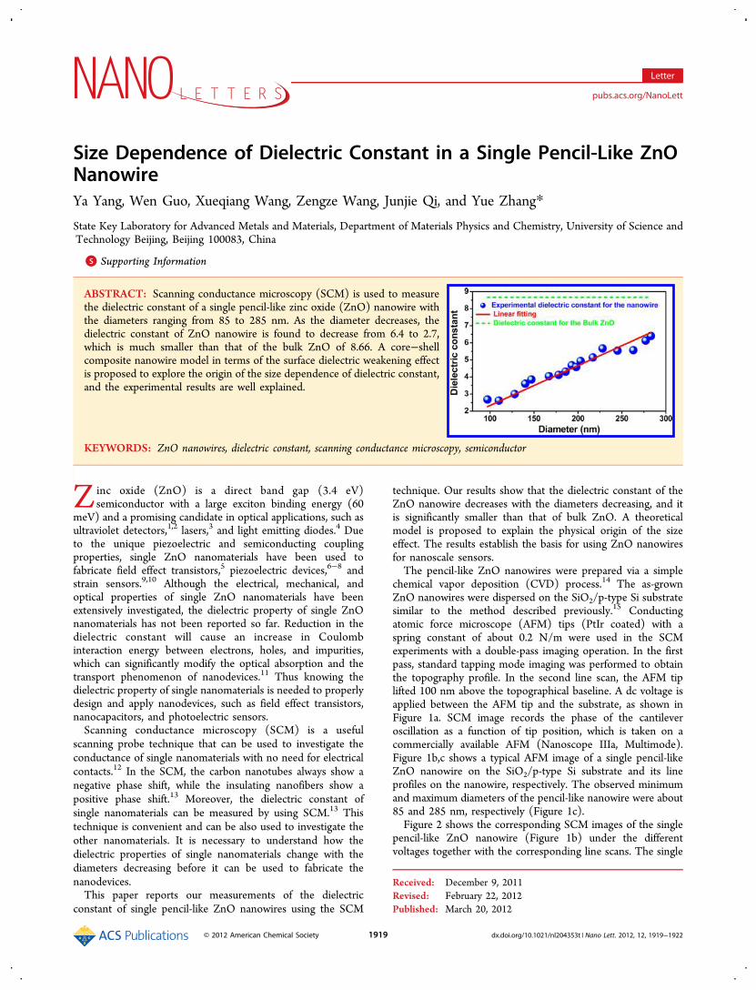
chemical vapor deposition (CVD) process.14 The as-grownZnO nanowires were dispersed on the SiO2/p-type Si substratesimilar to the method described previously.15 Conductingatomic force microscope (AFM) tips (PtIr coated) with aspring constant of about 0.2 N/m were used in the SCMexperiments with a double-pass imaging operation. In the firstpass, standard tapping mode imaging was performed to obtainthe topography profile. In the second line scan, the AFM tiplifted 100 nm above the topographical baseline. A dc voltage isapplied between the AFM tip and the substrate, as shown inFigure 1a. SCM image records the phase of the cantileveroscillation as a function of tip position, which is taken on acommercially available AFM (Nanoscope IIIa, Multimode).Figure 1b,c shows a typical AFM image of a single pencil-likeZnO nanowire on the SiO2/p-type Si substrate and its lineprofiles on the nanowire, respectively. The observed minimumand maximum diameters of the pencil-like nanowire were about85 and 285 nm, respectively (Figure 1c).Figure 2 shows the corresponding SCM images of the single
pencil-like ZnO nanowire (Figure 1b) under the differentvoltages together with the corresponding line scans. The single
Received: December 9, 2011Revised: February 22, 2012Published: March 20, 2012
Letter
pubs.acs.org/NanoLett
© 2012 American Chemical Society 1919 dx.doi.org/10.1021/nl204353t | Nano Lett. 2012, 12, 1919−1922
pencil-like nanowire shows a negative-positive-negative phaseshift (Figure 2), which is similar to the conducting nanofibers.16
SCM images were obtained in the interleave mode with thecantilever drive frequency of ω0 and the tip voltage of Vtip.When the AFM tip is scanned at height h above the sample andC(h) is the capacitance of the tip−sample system, theelectrostatic force F(h) = (1/2)C′(h)(Vtip + ϕ)2 can lead to achange of the resonant frequency of the cantilever and thephase difference between the driving force and the observedoscillation of the AFM tip, where ϕ is the work functiondifference between the tip and sample.17 Our results indicatethat the plane capacitor model is applicable for the pencil-likeZnO nanowire with the diameters from 100 to 300 nm at thelift height of 100 nm (see the Supporting Information). In thepresence of a force F between the AFM tip and the nanowire,the phase shift ΔΦ can be written as
ΔΦ = − + φ″ ″Qk
C h C h Vtan( )2
[ ( ) ( )]( )1 2 tip2
(1)
where Q = γw0 is the quality factor of the cantilever (γ, dampingcoefficient), k is the spring constant, and Ci″ (h) is the secondderivative of the capacitance of AFM tip−sample system (i = 1,AFM tip−SiO2/Si substrate; i = 2, AFM tip−ZnO nanowire−SiO2/Si substrate).
13 Over the bare SiO2/Si substrate, C1″ (h)can be given by
= ε π+ ε
″C h Rh t
( ) 2 ( )1
( / )1 0 tip
2
S3
(2)
where Rtip is the radius of the AFM tip, t is the thickness of theSiO2, and εS is the dielectric constant of the SiO2 [εS = 3.9].The AFM tip radius is about 20 nm, which was obtained fromthe analysis of the frequency “interaction image” in thenanocontact regime.18 When h = 100 nm and t = 200 nm,we find C1″(h) = 6.4 μF/m2 according to eq 2. For the AFMtip−nanowire−SiO2/Si substrate system, C1″(h) can be given by
= ε π+ ε + ε
″C h Rh t D
( ) 2 ( )1
( / / )f2 0 tip
2
S3
(3)
where D is the diameter of the nanowire, and εf is the dielectricconstant of ZnO nanowire.13
According to the eq 1, the tan(ΔΦ) ∝ (Vtip + ϕ)2
dependence is clearly seen for the pencil-like ZnO nanowirewith the different diameters in Figure 3. The dielectricconstants of the pencil-like ZnO nanowire can be obtainedby using the eqs 1−3, as shown in Figure 4. It is clearly seenthat the dielectric constant of the ZnO nanowire decreases withthe decreasing diameters, which is significantly lower than thatof the bulk ZnO [εbulk = 8.66].19 The dielectric constant willapproach the bulk value as the diameter is sufficiently large(Figure S6, Supporting Information). The size-dependentdielectric constant ε(D) can be given by
ε = +ε −+ Δ
DE E
( ) 11
1 ( / )bulk
g2
(4)
where Eg is the band gap of the material, and ΔE is change ofthe band gap.20 Usually, the quantum confinement effect canchange the band gap of nanomaterials when their sizes aresmaller than the exciton Bohr radius.21 However, the diametersof the pencil-like ZnO nanowires (85−285 nm) are obviouslylarger than the exciton Bohr radius (ZnO, ∼1.8 nm), indicatingthat the change of band gap due to quantum confinement effectcan be entirely neglected in this study. According to the eq 4,the dielectric constant cannot change as the diameters decreasefrom 285 to 85 nm, which is not consistent with theexperimental results in Figure 4.In order to investigate the surface effects on the dielectric
properties of ZnO nanowires, we performed additional forcefield theoretical calculation on both bulk and nanowire ZnO byusing simulation package GULP.22 The Lewis and Catlowpotentials were used in the atomistic simulations.23,24 Weobtained ZnO nanowire dielectric constants ε33 with thediameters from 1 to 10 nm, as shown in Figure 5. When thediameter of ZnO nanowire is 10 nm, the dielectric constant is5.23, which is close to the bulk value of 8.74. The resultindicates that the surface effect cannot be used to explain thelow dielectric constants for the large-size ZnO nanowires in theexperiments.To understand the origin of the size-dependent dielectric
constant of the pencil-like nanowire, the possible core−shellcomposite nanowire model was investigated. It has beenreported that a ZnO nanowire with modified surface layers canbe treated as a composite wire with a core−shell structurecomposed of a cylinder core and a surface shell (Figure 6),which has been used to explain the observed mechanical andelectrical properties in single ZnO nanowires.25,26 According tothe core−shell composite nanowire model, the total dielectricconstant εf can be quantitatively approximated by
ε =ε + Δ ε
Dd/ 2 /f
1 2 (5)
Figure 1. (a) A schematic diagram of SCM measurements. (b) AFMimage of a single pencil-like ZnO nanowire. (c) The correspondingline profiles of the pencil-like nanowire at the two ends of thenanowire.
Nano Letters Letter
dx.doi.org/10.1021/nl204353t | Nano Lett. 2012, 12, 1919−19221920

where d is the diameter of the core (unit, nm), Δ is depth of
the shell, and ε1 and ε2 are the dielectric constants of the core
and the shell, respectively (Figure 5).27 The ZnO nanowire can
be depleted completely or partly, depending on the wire
diameters.28 If the nanowire diameter is smaller than the width
of the surface depletion region, the nanowire will be thoroughly
depleted. It has been reported that the nanowire with the
diameter of 18 nm shows a “metallic” characteristic, indicating
that the depleted region has the main contribution to the
enhanced conductivity.29 The high conductivity will result in
the weakening of the dielectric property in the shell layer of the
nanowire. When the ε2 ≪ ε1, the total dielectric constant εf canbe expressed as
ε =εΔ
D2f
2(6)
According to the eq 6, it can be clearly seen that the linearchange of the dielectric constant versus the ZnO diameterdescribed by the core−shell composite nanowire model iscompletely consistent with the experimental results in Figure 4.Our results indicate that the decrease of the dielectric constantis mainly due to the existence of the shell layer in the ZnO
Figure 2. (a,c,e) The SCM images of the pencil-like ZnO nanowire under the voltages of 0, 4, and 8 V, respectively. The corresponding line profilesalong the white dashed line are shown in (b,d,f), respectively.
Figure 3. The tan(ΔΦ) versus (Vtip + ϕ)2 for the single pencil-likeZnO nanowire.
Figure 4. Diameter dependence of dielectric constant in the singlepencil-like ZnO nanowire: (blue dot) experimental results, (red solidline) fitted results by core−shell composite nanowire model, and(green dashed line) dielectric constant of bulk ZnO.
Nano Letters Letter
dx.doi.org/10.1021/nl204353t | Nano Lett. 2012, 12, 1919−19221921

nanowires, which is of great importance for designing andapplying the nanodevice based on single ZnO nanomaterials.In summary, a size dependence of dielectric constant in
single pencil-like ZnO nanowires is experimentally revealed.The dielectric constant decreases dramatically with decreasingdiameters and is significantly lower than that of the bulk ZnO.The size dependence of dielectric constant is well explained byan approximate core−shell composite nanowire model in termsof the surface dielectric weakening effect. The results supportthe applications of ZnO nanomaterials as nanoscale electricdevices.
■ ASSOCIATED CONTENT*S Supporting InformationThe plane-capacitor model in AFM tip-ZnO nanowire-SiO2/Sisubstrate system, the AFM image, and the corresponding SCMimage of a single pencil-like ZnO nanowire. This material isavailable free of charge via the Internet at http://pubs.acs.org.
■ AUTHOR INFORMATIONCorresponding Author*E-mail: [email protected] authors declare no competing financial interest.
■ ACKNOWLEDGMENTSThis work was supported by the Major Project of InternationalCooperation and Exchanges (2006DFB51000), the NationalNatural Science Foundation of China (51172022), theResearch Fund of Co-construction Program from Beijing
Municipal Commission of Education, the FundamentalResearch Funds for the Central Universities.
■ REFERENCES(1) Yang, Q.; Guo, X.; Wang, W.; Zhang, Y.; Xu, S.; Lien, D. H.;Wang, Z. L. ACS Nano 2010, 4, 6285.(2) Soci, C; Zhang, A.; Xiang, B.; Dayeh, S. A.; Aplin, D. P. R; Park,J.; Bao, X. Y.; Lo, Y. H.; Wang, D. Nano Lett. 2007, 7, 1003.(3) Chu, S.; Wang, W.; Zhou, W.; Lin, Y.; Chernyak, L.; Zhao, J.;Kong, J.; Li, L.; Ren, J.; Liu, J. Nat. Nanotechnol. 2011, 6, 506.(4) Ryu, Y.; Lee, T. S.; Lubguban, J. A.; White, H. W.; Kim, B. J.;Park, Y. S. Appl. Phys. Lett. 2006, 88, 241108.(5) Fei, P.; Yeh, P.; Zhou, J.; Xu, S.; Gao, Y.; Song, J.; Gu, Y.; Huang,Y.; Wang, Z. L. Nano Lett. 2009, 9, 3435.(6) Wang, Z. L.; Song, J. H. Science 2006, 312, 242.(7) Qin, Y.; Wang, X. D.; Wang, Z. L. Nature 2008, 451, 809.(8) Yang, R. S.; Qin, Y.; Li, C.; Zhu, G.; Wang, Z. L. Nano Lett. 2009,9, 1201.(9) Wang, X. D.; Zhou, J.; Song, J. H.; Liu, J.; Xu, N. S.; Wang, Z. L.Nano Lett. 2006, 6, 2768.(10) Yang, Y.; Qi, J. J.; Zhang, Y.; Liao, Q. L.; Tang, L. D.; Qin, Z.Appl. Phys. Lett. 2008, 92, 183117.(11) Sharma, A. C. J. Appl. Phys. 2006, 100, 084301.(12) Bockrath, M.; Markovic, N.; Shepard, A.; Tinkham, M.;Gurevich, L.; Kouwenhoven, L. P.; Wu, M. W.; Sohn, L. L. NanoLett. 2002, 2, 187.(13) Staii, C.; Johnson, A. T.; Pinto, N. J. Nano Lett. 2004, 4, 859.(14) Yang, Y. H.; Chen, X. Y.; Feng, Y.; Yang, G. W. Nano Lett. 2007,7, 3879.(15) Yang, Y.; Zhang, Y.; Qi, J. J.; Liao, Q. L.; Tang, L. D.; Wang, Y.S. J. Appl. Phys. 2009, 105, 084319.(16) Zhou, Y. X.; Freitag, M.; Hone, J.; Staii, C.; Pinto, N. J.;MacDiarmid, A. G. Appl. Phys. Lett. 2003, 83, 3800.(17) Bachtold, A.; Fuhrer, M. S.; Plyasunov, S.; Forero, M.;Anderson, E. H.; Zettl, A.; McEuen, P. L. Phys. Rev. Lett. 2000, 84,6082.(18) Palacios-Lidon, E.; Colchero, J. Nanotechnology 2006, 17, 5491.(19) Fan, Z.; Lu, J. G. J. Nanosci. Nanotechnol. 2005, 5, 1561.(20) Tsu, R.; Babic, D.; Ioriatti, L. J. Appl. Phys. 1997, 82, 1327.(21) Yu, H.; Li, J.; Loomis, R. A.; Gibbons, P. C.; Wang, W. L.;Buhro, W. E. J. Am. Chem. Soc. 2003, 125, 16168.(22) Gale, J. D. J. Chem. Soc., Faraday Trans. 1997, 93, 629.(23) Combe, N.; Chassaing, P. -M.; Demangeot, F. Phys. Rev. B 2009,79, 045408.(24) Lewis, G. V.; Catlow, C. R. A. J. Phys. C 1985, 18, 1149.(25) Chen, C. Q.; Shi, Y.; Zhang, Y. S.; Zhu, J.; Yan, Y. J. Phys. Rev.Lett. 2006, 96, 075505.(26) Hong, W. K.; Sohn, J. I.; Hwang, D. K.; Kwon, S. S.; Jo, G.;Song, S.; Kim, S. M.; Ko, H. J.; Park, S. J.; Welland, M. E.; Lee, T.Nano Lett. 2008, 8, 950.(27) Liu, Y. H.; Jiang, L.; Zhao, R. J.; Nan, C. W. Phys. Rev. B 2005,72, 014103.(28) Gao, P.; Wang, Z. Z.; Liu, K. H.; Xu, Z.; Wang, W. L.; Bai, X. D.;Wang, E. G. J. Mater. Chem. 2009, 19, 1002.(29) Chang, P. C.; Chien, C. J.; Stichtenoth, D.; Ronning, C.; Lu, J.G. Appl. Phys. Lett. 2007, 90, 113101.
Figure 5. Diameter dependence of dielectric constant ε33 in ZnOnanowires by using the theoretical calculation.The inset shows a ZnOnanowire model image along [0001] direction with a diameter of 3nm.
Figure 6. Schematic illustration of the core−shell composite nanowiremodel.
Nano Letters Letter
dx.doi.org/10.1021/nl204353t | Nano Lett. 2012, 12, 1919−19221922