Embed Size (px)
Citation preview
ST
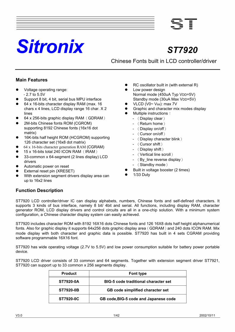
Sitronix ST7920 Chinese Fonts built in LCD controller/driver
V3.0 1/42 2002/10/11
Main Features
Voltage operating range: - 2.7 to 5.5V
Support 8 bit, 4 bit, serial bus MPU interface 64 x 16-bits character display RAM (max. 16
chars x 4 lines, LCD display range 16 char. X 2 lines
64 x 256-bits graphic display RAM(GDRAM) 2M-bits Chinese fonts ROM (CGROM)
supporting 8192 Chinese fonts (16x16 dot matrix)
16K-bits half height ROM (HCGROM) supporting 126 character set (16x8 dot matrix)
64 x 16-bits character generation RAM (CGRAM) 15 x 16-bits total 240 ICON RAM(IRAM) 33-common x 64-segment (2 lines display) LCD
drivers Automatic power on reset External reset pin (XRESET) With extension segment drivers display area can
up to 16x2 lines
RC oscillator built in (with external R) Low power design
Normal mode (450uA Typ VDD=5V) Standby mode (30uA Max VDD=5V)
VLCD (V0~ Vss): max 7V Graphic and character mix modes display Multiple instructions:
- (Display clear) - (Return home) - (Display on/off) - (Cursor on/off) - (Display character blink) - (Cursor shift) - (Display shift) - (Vertical line scroll) - (By_line reverse display) - (Standby mode)
Built in voltage booster (2 times) 1/33 Duty
Function Description ST7920 LCD controller/driver IC can display alphabets, numbers, Chinese fonts and self-defined characters. It supports 3 kinds of bus interface, namely 8 bit/ 4bit and serial. All functions, including display RAM, character generator ROM, LCD display drivers and control circuits are all in a one-chip solution. With a minimum system configuration, a Chinese character display system can easily achieved. ST7920 includes character ROM with 8192 16X16 dots Chinese fonts and 126 16X8 dots half height alphanumerical fonts. Also for graphic display it supports 64x256 dots graphic display area(GDRAM)and 240 dots ICON RAM. Mix mode display with both character and graphic data is possible. ST7920 has built in 4 sets CGRAM providing software programmable 16X16 font. ST7920 has wide operating voltage (2.7V to 5.5V) and low power consumption suitable for battery power portable device. ST7920 LCD driver consists of 33 common and 64 segments. Together with extension segment driver ST7921, ST7920 can support up to 33 common x 256 segments display.
Product Font type
ST7920-0A BIG-5 code traditional character set
ST7920-0B GB code simplified character set
ST7920-0C GB code,BIG-5 code and Japanese code
ST7920
V3.0 2/42 2002/10/11
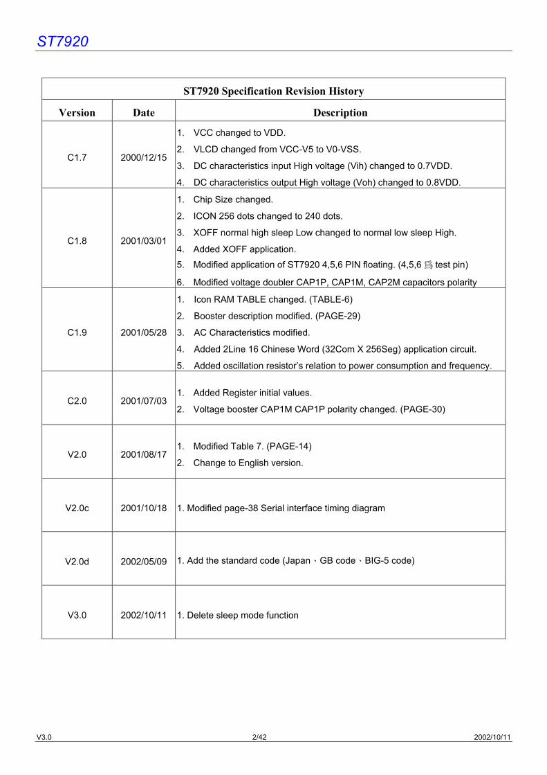
ST7920 Specification Revision History
Version Date Description
C1.7 2000/12/15
1. VCC changed to VDD.
2. VLCD changed from VCC-V5 to V0-VSS.
3. DC characteristics input High voltage (Vih) changed to 0.7VDD.
4. DC characteristics output High voltage (Voh) changed to 0.8VDD.
C1.8 2001/03/01
1. Chip Size changed.
2. ICON 256 dots changed to 240 dots.
3. XOFF normal high sleep Low changed to normal low sleep High.
4. Added XOFF application. 5. Modified application of ST7920 4,5,6 PIN floating. (4,5,6 為 test pin)
6. Modified voltage doubler CAP1P, CAP1M, CAP2M capacitors polarity
C1.9 2001/05/28
1. Icon RAM TABLE changed. (TABLE-6)
2. Booster description modified. (PAGE-29)
3. AC Characteristics modified.
4. Added 2Line 16 Chinese Word (32Com X 256Seg) application circuit.
5. Added oscillation resistor’s relation to power consumption and frequency.
C2.0 2001/07/03 1. Added Register initial values.
2. Voltage booster CAP1M CAP1P polarity changed. (PAGE-30)
V2.0 2001/08/17 1. Modified Table 7. (PAGE-14)
2. Change to English version.
V2.0c 2001/10/18 1. Modified page-38 Serial interface timing diagram
V2.0d 2002/05/09 1. Add the standard code (Japan、GB code、BIG-5 code)
V3.0 2002/10/11 1. Delete sleep mode function
ST7920
V3.0 3/42 2002/10/11
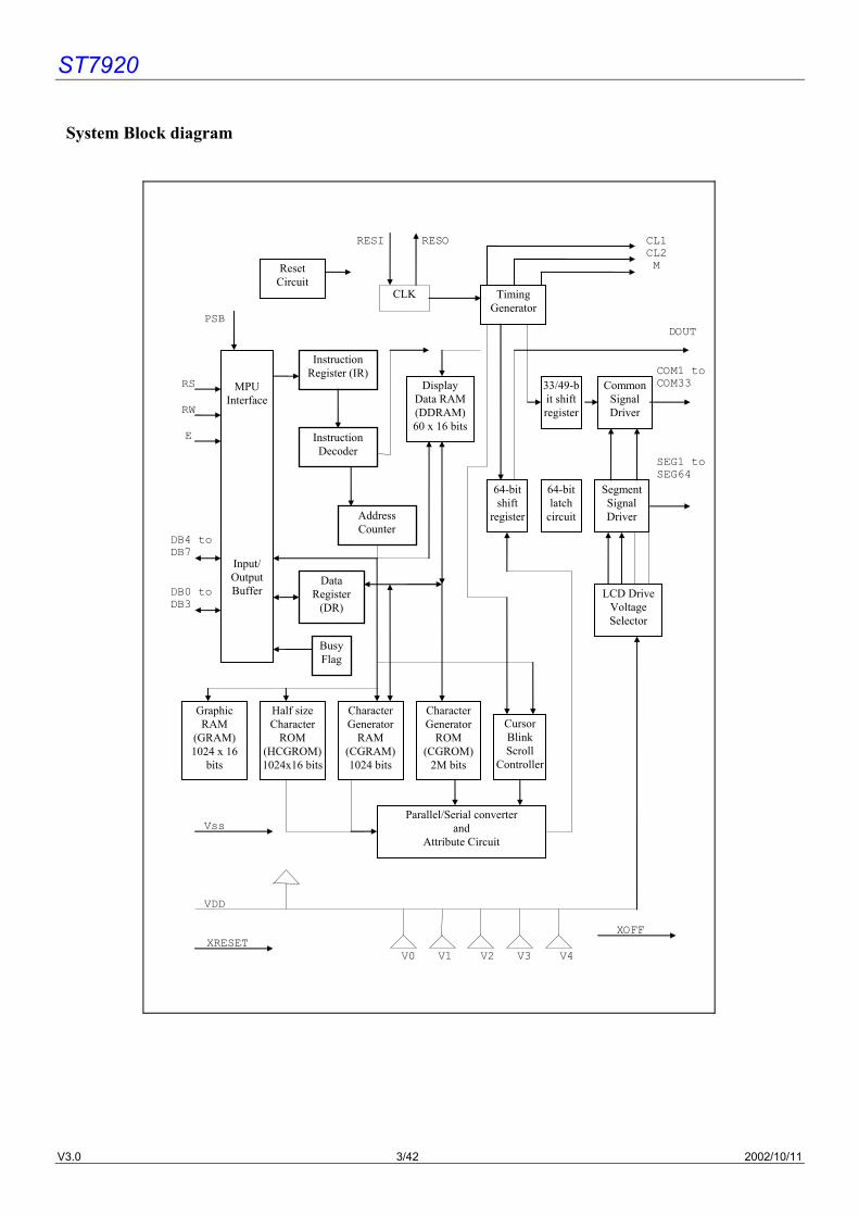
System Block diagram
Timing Generator
33/49-bit shift register
Common Signal Driver
Display Data RAM(DDRAM)60 x 16 bits
64-bit latch
circuit
Segment Signal Driver
64-bit shift
register
LCD Drive Voltage Selector
CLK
Instruction Register (IR)
Instruction Decoder
Reset Circuit
MPU Interface
Input/ Output Buffer
Address Counter
Character Generator
ROM (CGROM)
2M bits
Character Generator
RAM (CGRAM)1024 bits
Cursor Blink Scroll
Controller
Data Register
(DR)
Busy Flag
Parallel/Serial converter and
Attribute Circuit
VDD
V0 V1 V2 V3 V4
RESI RESO CL1 CL2 M
DOUT
COM1 to COM33
SEG1 to SEG64
RS
RW
E
DB4 to DB7
DB0 to DB3
Half size Character
ROM (HCGROM) 1024x16 bits
XRESET
Graphic RAM
(GRAM) 1024 x 16
bits
XOFF
Vss
PSB
ST7920
V3.0 4/42 2002/10/11
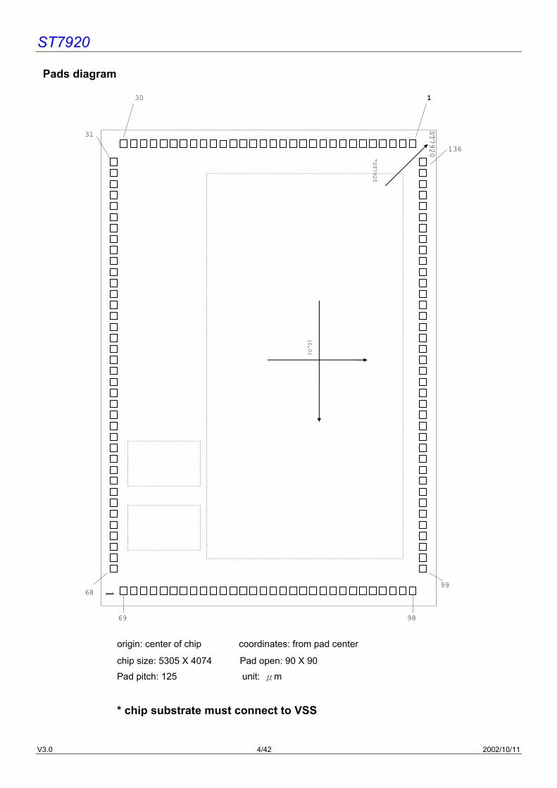
Pads diagram
origin: center of chip coordinates: from pad center
chip size: 5305 X 4074 Pad open: 90 X 90 Pad pitch: 125 unit: μm
* chip substrate must connect to VSS
98 69
136
30
31
1
68 99
ST7920 “ST7920
(0,0)
1
ST7920
V3.0 5/42 2002/10/11
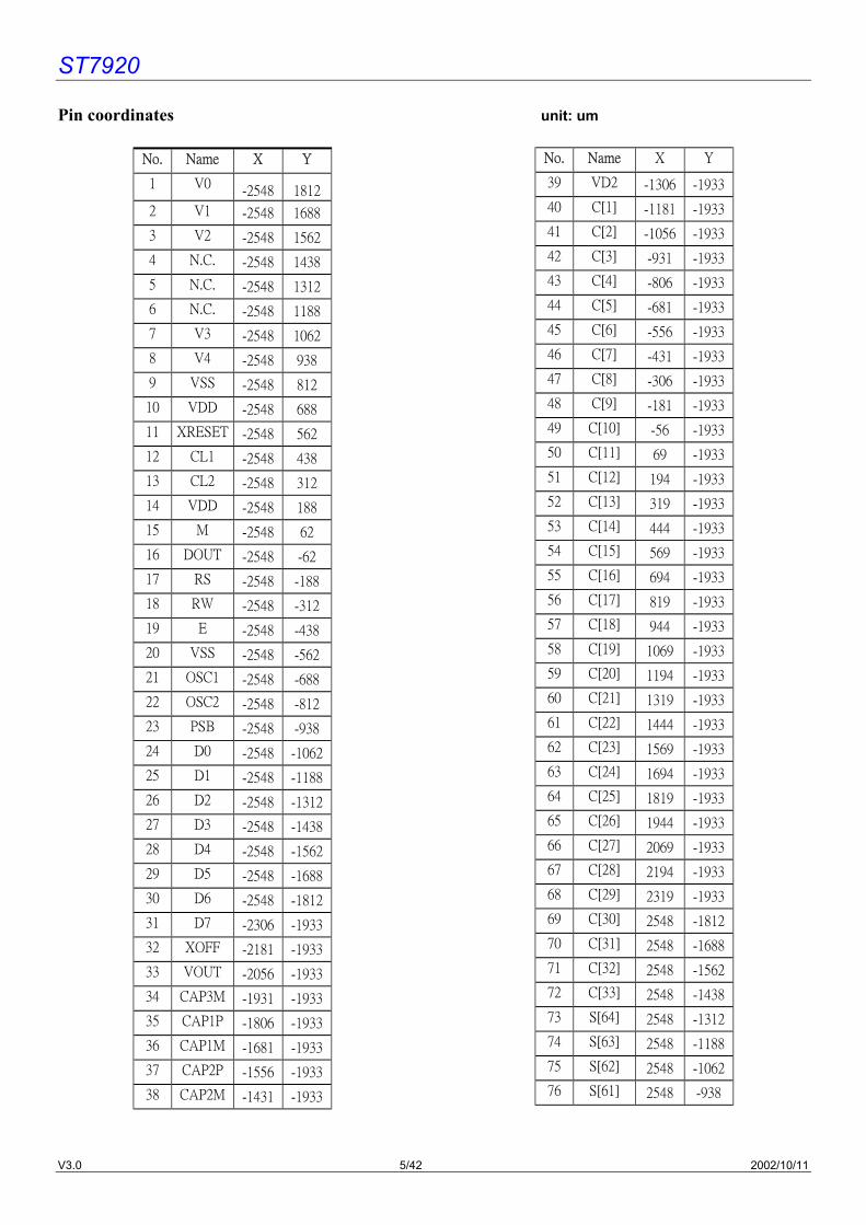
Pin coordinates unit: um
No. Name X Y
1 V0 -2548 1812
2 V1 -2548 1688
3 V2 -2548 1562
4 N.C. -2548 1438
5 N.C. -2548 1312
6 N.C. -2548 1188
7 V3 -2548 1062
8 V4 -2548 938
9 VSS -2548 812
10 VDD -2548 688
11 XRESET -2548 562
12 CL1 -2548 438
13 CL2 -2548 312
14 VDD -2548 188
15 M -2548 62
16 DOUT -2548 -62
17 RS -2548 -188
18 RW -2548 -312
19 E -2548 -438
20 VSS -2548 -562
21 OSC1 -2548 -688
22 OSC2 -2548 -812
23 PSB -2548 -938
24 D0 -2548 -1062
25 D1 -2548 -1188
26 D2 -2548 -1312
27 D3 -2548 -1438
28 D4 -2548 -1562
29 D5 -2548 -1688
30 D6 -2548 -1812
31 D7 -2306 -1933
32 XOFF -2181 -1933
33 VOUT -2056 -1933
34 CAP3M -1931 -1933
35 CAP1P -1806 -1933
36 CAP1M -1681 -1933
37 CAP2P -1556 -1933
38 CAP2M -1431 -1933
No. Name X Y
39 VD2 -1306 -1933
40 C[1] -1181 -1933
41 C[2] -1056 -1933
42 C[3] -931 -1933
43 C[4] -806 -1933
44 C[5] -681 -1933
45 C[6] -556 -1933
46 C[7] -431 -1933
47 C[8] -306 -1933
48 C[9] -181 -1933
49 C[10] -56 -1933
50 C[11] 69 -1933
51 C[12] 194 -1933
52 C[13] 319 -1933
53 C[14] 444 -1933
54 C[15] 569 -1933
55 C[16] 694 -1933
56 C[17] 819 -1933
57 C[18] 944 -1933
58 C[19] 1069 -1933
59 C[20] 1194 -1933
60 C[21] 1319 -1933
61 C[22] 1444 -1933
62 C[23] 1569 -1933
63 C[24] 1694 -1933
64 C[25] 1819 -1933
65 C[26] 1944 -1933
66 C[27] 2069 -1933
67 C[28] 2194 -1933
68 C[29] 2319 -1933
69 C[30] 2548 -1812
70 C[31] 2548 -1688
71 C[32] 2548 -1562
72 C[33] 2548 -1438
73 S[64] 2548 -1312
74 S[63] 2548 -1188
75 S[62] 2548 -1062
76 S[61] 2548 -938
ST7920
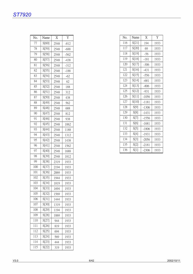
V3.0 6/42 2002/10/11
No. Name X Y
77 S[60] 2548 -812
78 S[59] 2548 -688
79 S[58] 2548 -562
80 S[57] 2548 -438
81 S[56] 2548 -312
82 S[55] 2548 -188
83 S[54] 2548 -62
84 S[53] 2548 62
85 S[52] 2548 188
86 S[51] 2548 312
87 S[50] 2548 438
88 S[49] 2548 562
89 S[48] 2548 688
90 S[47] 2548 812
91 S[46] 2548 938
92 S[45] 2548 1062
93 S[44] 2548 1188
94 S[43] 2548 1312
95 S[42] 2548 1438
96 S[41] 2548 1562
97 S[40] 2548 1688
98 S[39] 2548 1812
99 S[38] 2319 1933
100 S[37] 2194 1933
101 S[36] 2069 1933
102 S[35] 1944 1933
103 S[34] 1819 1933
104 S[33] 1694 1933
105 S[32] 1569 1933
106 S[31] 1444 1933
107 S[30] 1319 1933
108 S[29] 1194 1933
109 S[28] 1069 1933
110 S[27] 944 1933
111 S[26] 819 1933
112 S[25] 694 1933
113 S[24] 569 1933
114 S[23] 444 1933
115 S[22] 319 1933
No. Name X Y
116 S[21] 194 1933
117 S[20] 69 1933
118 S[19] -56 1933
119 S[18] -181 1933
120 S[17] -306 1933
121 S[16] -431 1933
122 S[15] -556 1933
123 S[14] -681 1933
124 S[13] -806 1933
125 S[12] -931 1933
126 S[11] -1056 1933
127 S[10] -1181 1933
128 S[9] -1306 1933
129 S[8] -1431 1933
130 S[7] -1556 1933
131 S[6] -1681 1933
132 S[5] -1806 1933
133 S[4] -1931 1933
134 S[3] -2056 1933
135 S[2] -2181 1933
136 S[1] -2306 1933
ST7920
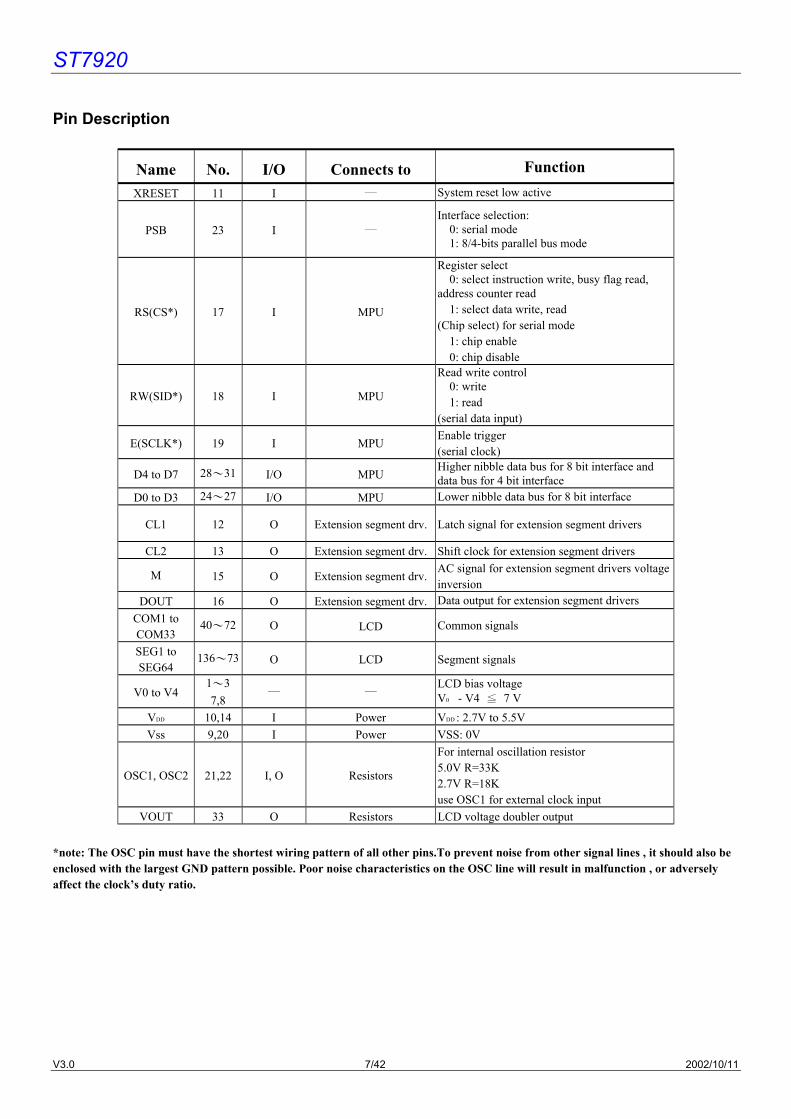
V3.0 7/42 2002/10/11
Pin Description
Name No. I/O Connects to Function XRESET 11 I ― System reset low active
PSB 23 I ― Interface selection:
0: serial mode 1: 8/4-bits parallel bus mode
RS(CS*) 17 I MPU
Register select 0: select instruction write, busy flag read,
address counter read 1: select data write, read
(Chip select) for serial mode 1: chip enable 0: chip disable
RW(SID*) 18 I MPU
Read write control 0: write 1: read
(serial data input)
E(SCLK*) 19 I MPU Enable trigger (serial clock)
D4 to D7 28〜31 I/O MPU Higher nibble data bus for 8 bit interface and data bus for 4 bit interface
D0 to D3 24〜27 I/O MPU Lower nibble data bus for 8 bit interface
CL1 12 O Extension segment drv. Latch signal for extension segment drivers
CL2 13 O Extension segment drv. Shift clock for extension segment drivers
M 15 O Extension segment drv.AC signal for extension segment drivers voltage inversion
DOUT 16 O Extension segment drv. Data output for extension segment drivers COM1 to COM33
40〜72 O LCD Common signals
SEG1 to SEG64
136〜73 O LCD Segment signals
V0 to V4 1〜3 7,8
― ― LCD bias voltage V0 - V4 ≦ 7 V
VDD 10,14 I Power VDD : 2.7V to 5.5V Vss 9,20 I Power VSS: 0V
OSC1, OSC2 21,22 I, O Resistors
For internal oscillation resistor 5.0V R=33K 2.7V R=18K use OSC1 for external clock input
VOUT 33 O Resistors LCD voltage doubler output *note: The OSC pin must have the shortest wiring pattern of all other pins.To prevent noise from other signal lines , it should also be enclosed with the largest GND pattern possible. Poor noise characteristics on the OSC line will result in malfunction , or adversely affect the clock’s duty ratio.
ST7920
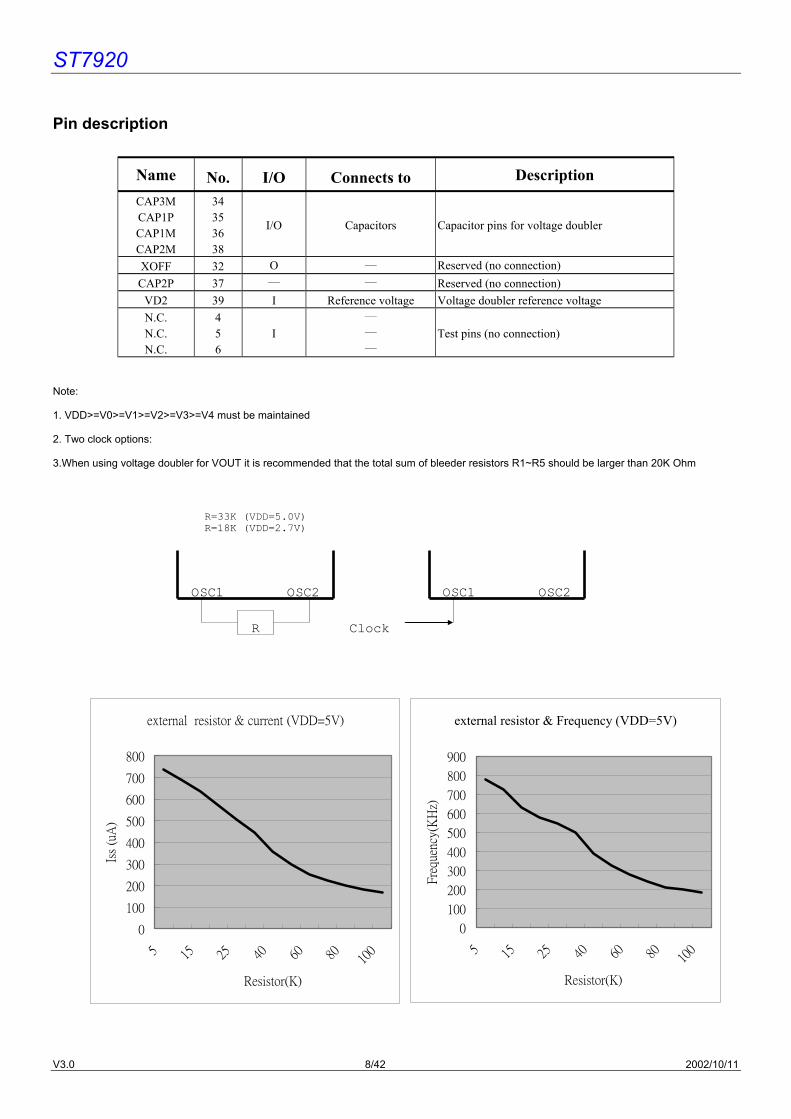
V3.0 8/42 2002/10/11
external resistor & current (VDD=5V)
0
100
200
300
400
500
600
700
800
5 15 25 40 60 80 100
Resistor(K)
Iss
(uA
)
external resistor & Frequency (VDD=5V)
0
100
200
300
400
500
600
700
800
900
5 15 25 40 60 80 100
Resistor(K)
Fre
quen
cy(K
Hz)
Pin description
Name No. I/O Connects to Description CAP3M CAP1P CAP1M CAP2M
34 35 36 38
I/O Capacitors Capacitor pins for voltage doubler
XOFF 32 O ― Reserved (no connection) CAP2P 37 ― ― Reserved (no connection)
VD2 39 I Reference voltage Voltage doubler reference voltage N.C. N.C. N.C.
4 5 6
I ― ― ―
Test pins (no connection)
Note:
1. VDD>=V0>=V1>=V2>=V3>=V4 must be maintained
2. Two clock options:
3.When using voltage doubler for VOUT it is recommended that the total sum of bleeder resistors R1~R5 should be larger than 20K Ohm
R
OSC1 OSC2 OSC1 OSC2
Clock
R=33K (VDD=5.0V) R=18K (VDD=2.7V)
ST7920
V3.0 9/42 2002/10/11
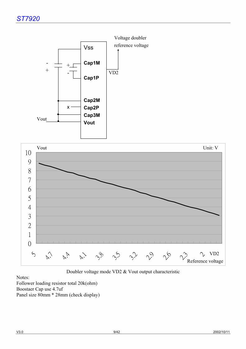
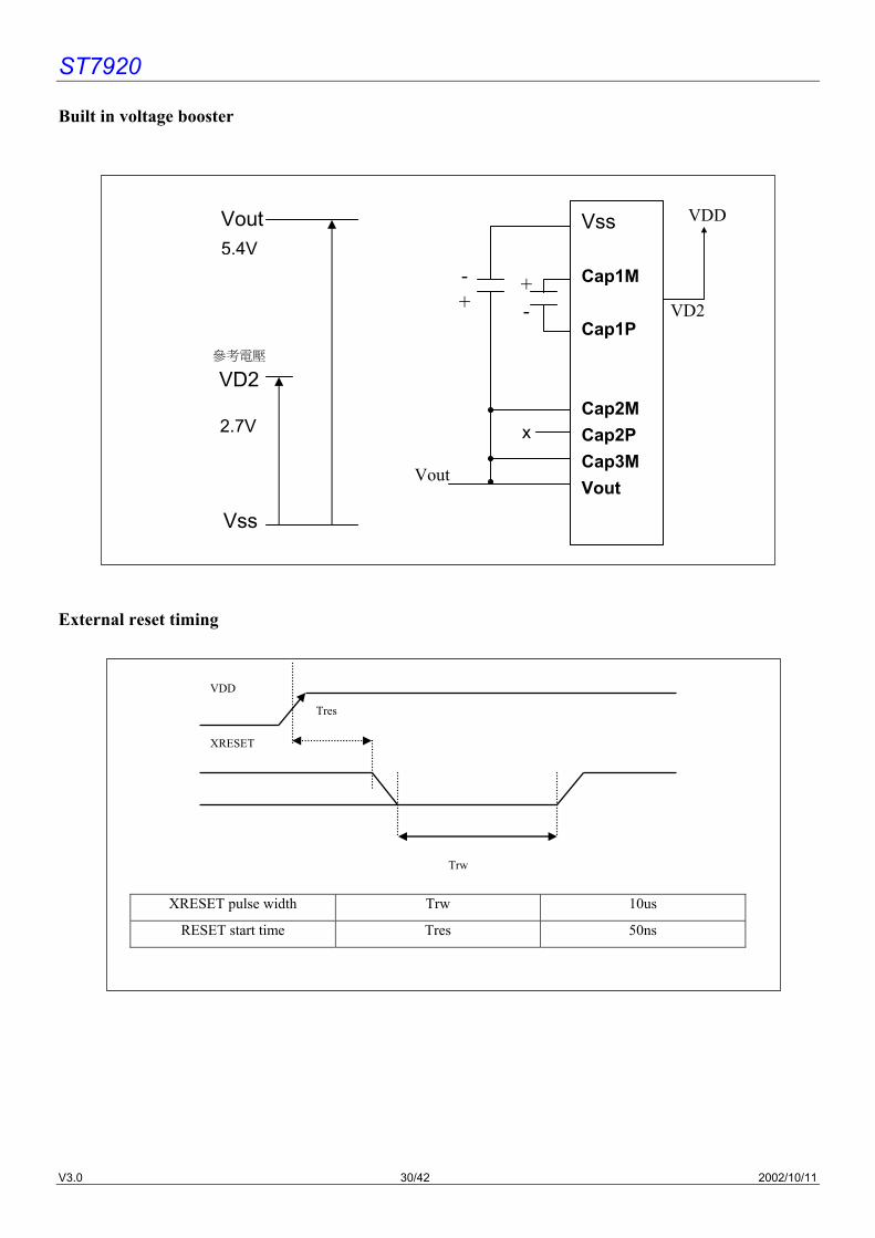
Doubler voltage mode VD2 & Vout output characteristic Notes: Follower loading resistor total 20k(ohm) Boostaer Cap use 4.7uf Panel size 80mm * 28mm (check display)
Vss Cap1M Cap1P Cap2M Cap2P Cap3M Vout
+-
- +
x
Vout
Voltage doubler reference voltage
VD2
0
1
2
3
4
5
6
7
8
9
10
5 4.7
4.4
4.1
3.8
3.5
3.2
2.9
2.6
2.3 2 VD2 Reference voltage
Vout Unit: V
ST7920
V3.0 10/42 2002/10/11
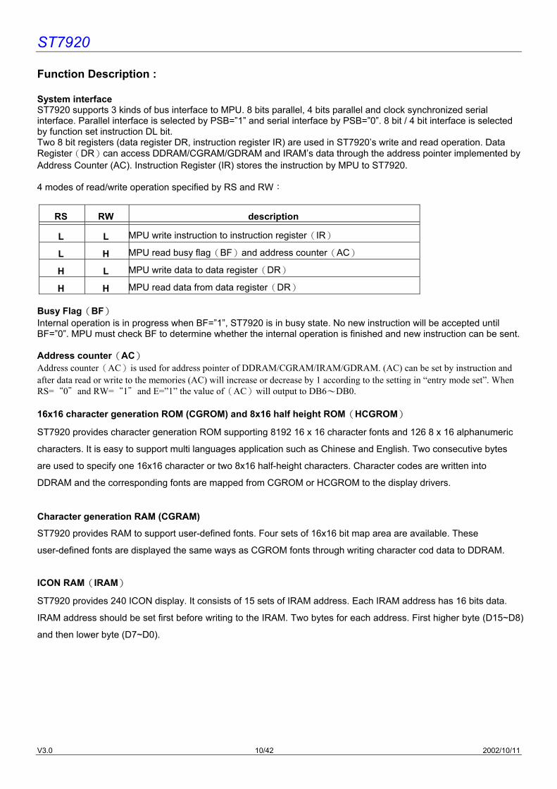
Function Description : System interface ST7920 supports 3 kinds of bus interface to MPU. 8 bits parallel, 4 bits parallel and clock synchronized serial interface. Parallel interface is selected by PSB=”1” and serial interface by PSB=”0”. 8 bit / 4 bit interface is selected by function set instruction DL bit. Two 8 bit registers (data register DR, instruction register IR) are used in ST7920’s write and read operation. Data Register(DR)can access DDRAM/CGRAM/GDRAM and IRAM’s data through the address pointer implemented by Address Counter (AC). Instruction Register (IR) stores the instruction by MPU to ST7920. 4 modes of read/write operation specified by RS and RW:
RS RW description
L L MPU write instruction to instruction register(IR)
L H MPU read busy flag(BF)and address counter(AC)
H L MPU write data to data register(DR)
H H MPU read data from data register(DR) Busy Flag(BF) Internal operation is in progress when BF=”1”, ST7920 is in busy state. No new instruction will be accepted until BF=”0”. MPU must check BF to determine whether the internal operation is finished and new instruction can be sent. Address counter(AC) Address counter(AC)is used for address pointer of DDRAM/CGRAM/IRAM/GDRAM. (AC) can be set by instruction and after data read or write to the memories (AC) will increase or decrease by 1 according to the setting in “entry mode set”. When RS=“0”and RW=“1”and E=”1” the value of(AC)will output to DB6〜DB0. 16x16 character generation ROM (CGROM) and 8x16 half height ROM(HCGROM)
ST7920 provides character generation ROM supporting 8192 16 x 16 character fonts and 126 8 x 16 alphanumeric
characters. It is easy to support multi languages application such as Chinese and English. Two consecutive bytes
are used to specify one 16x16 character or two 8x16 half-height characters. Character codes are written into
DDRAM and the corresponding fonts are mapped from CGROM or HCGROM to the display drivers.
Character generation RAM (CGRAM)
ST7920 provides RAM to support user-defined fonts. Four sets of 16x16 bit map area are available. These
user-defined fonts are displayed the same ways as CGROM fonts through writing character cod data to DDRAM.
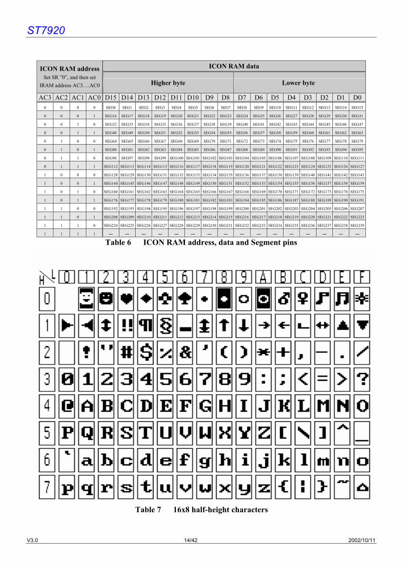
ICON RAM(IRAM)
ST7920 provides 240 ICON display. It consists of 15 sets of IRAM address. Each IRAM address has 16 bits data.
IRAM address should be set first before writing to the IRAM. Two bytes for each address. First higher byte (D15~D8)
and then lower byte (D7~D0).
ST7920
V3.0 11/42 2002/10/11
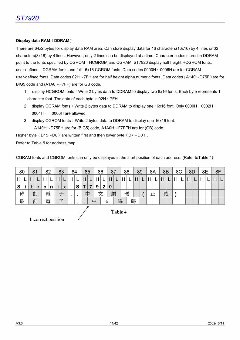
Table 4
Display data RAM(DDRAM)
There are 64x2 bytes for display data RAM area. Can store display data for 16 characters(16x16) by 4 lines or 32
characters(8x16) by 4 lines. However, only 2 lines can be displayed at a time. Character codes stored in DDRAM point to the fonts specified by CGROM,HCGROM and CGRAM. ST7920 display half height HCGROM fonts,
user-defined CGRAM fonts and full 16x16 CGROM fonts. Data codes 0000H〜0006H are for CGRAM
user-defined fonts. Data codes 02H〜7FH are for half height alpha numeric fonts. Data codes(A140〜D75F)are for
BIG5 code and (A1A0〜F7FF) are for GB code.
1. display HCGROM fonts:Write 2 bytes data to DDRAM to display two 8x16 fonts. Each byte represents 1
character font. The data of each byte is 02H〜7FH.
2. display CGRAM fonts:Write 2 bytes data to DDRAM to display one 16x16 font. Only 0000H,0002H,
0004H, 0006H are allowed.
3. display CGROM fonts:Write 2 bytes data to DDRAM to display one 16x16 font.
A140H〜D75FH are for (BIG5) code, A1A0H〜F7FFH are for (GB) code.
Higher byte(D15〜D8)are written first and then lower byte(D7〜D0).
Refer to Table 5 for address map
CGRAM fonts and CGROM fonts can only be displayed in the start position of each address. (Refer toTable 4)
80 81 82 83 84 85 86 87 88 89 8A 8B 8C 8D 8E 8F H L H L H L H L H L H L H L H L H L H L H L H L H L H L H L H LS i t r o n i x S T 7 9 2 0 矽 創 電 子 . . 中 文 編 碼 ( 正 確 ) 矽 創 電 子 . . . 中 文 編 碼
Incorrect position
ST7920
V3.0 12/42 2002/10/11
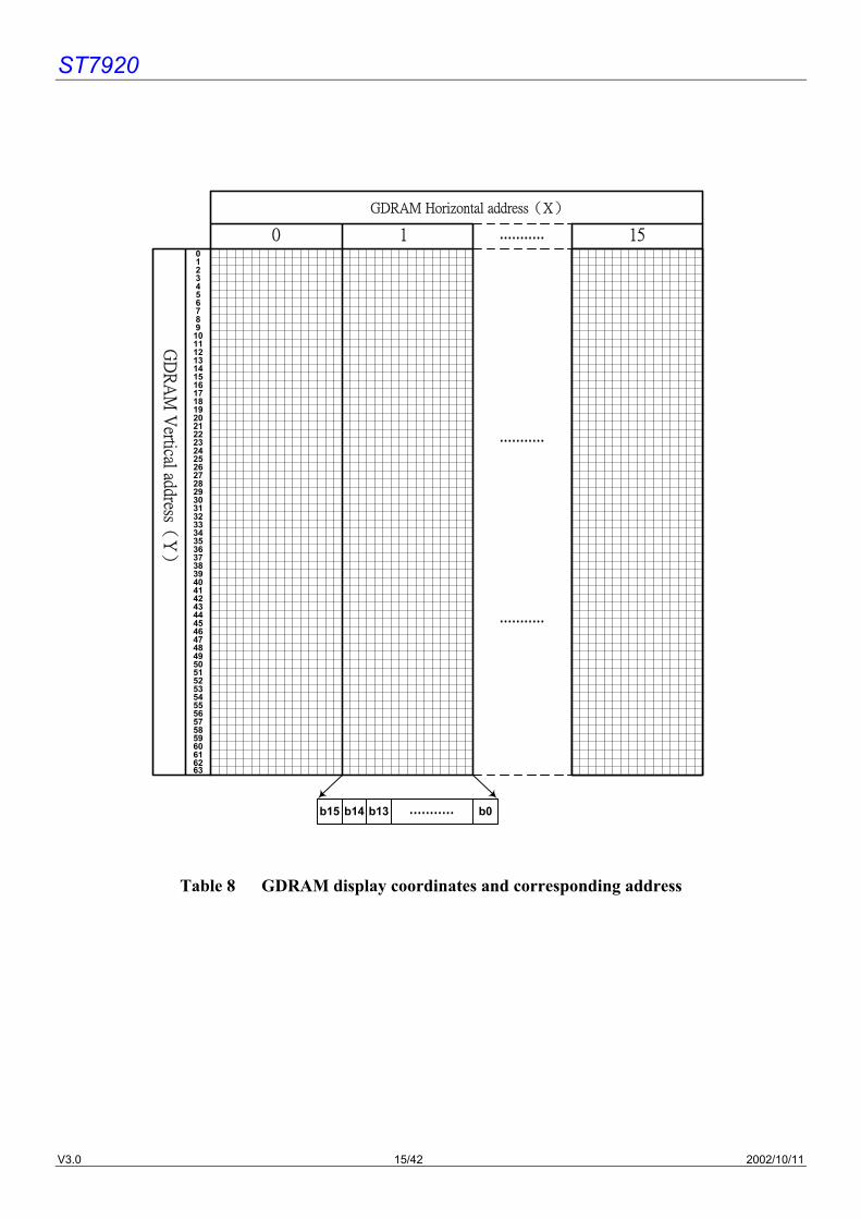
Graphic RAM(GDRAM)
Graphic display RAM supports 64x256 bits bit-mapped memory space. GDRAM address is set by writing 2
consecutive bytes for vertical address and horizontal address. Two-bytes data write to GDRAM for one address.
Address counter will automatically increase by one for the next two-byte data. The procedure is as followings. 1. Set vertical address(Y)for GDRAM
2. Set horizontal address(X)for GDRAM
3. Write D15〜D8 to GDRAM 中(first byte)
4. Write D7〜D0 to GDRAM 中(second byte)
Graphic display memory map please refer to Table-8
LCD driver
LCD driver have 33 common and 64 segments to drive the LCD panel. Segment data from CGRAM /CGROM
/HCGROM are shifted into the 64 bits segment latches to display. Extended segment driver ST7921 can be used to
extend the segment drivers to 256.
ST7920
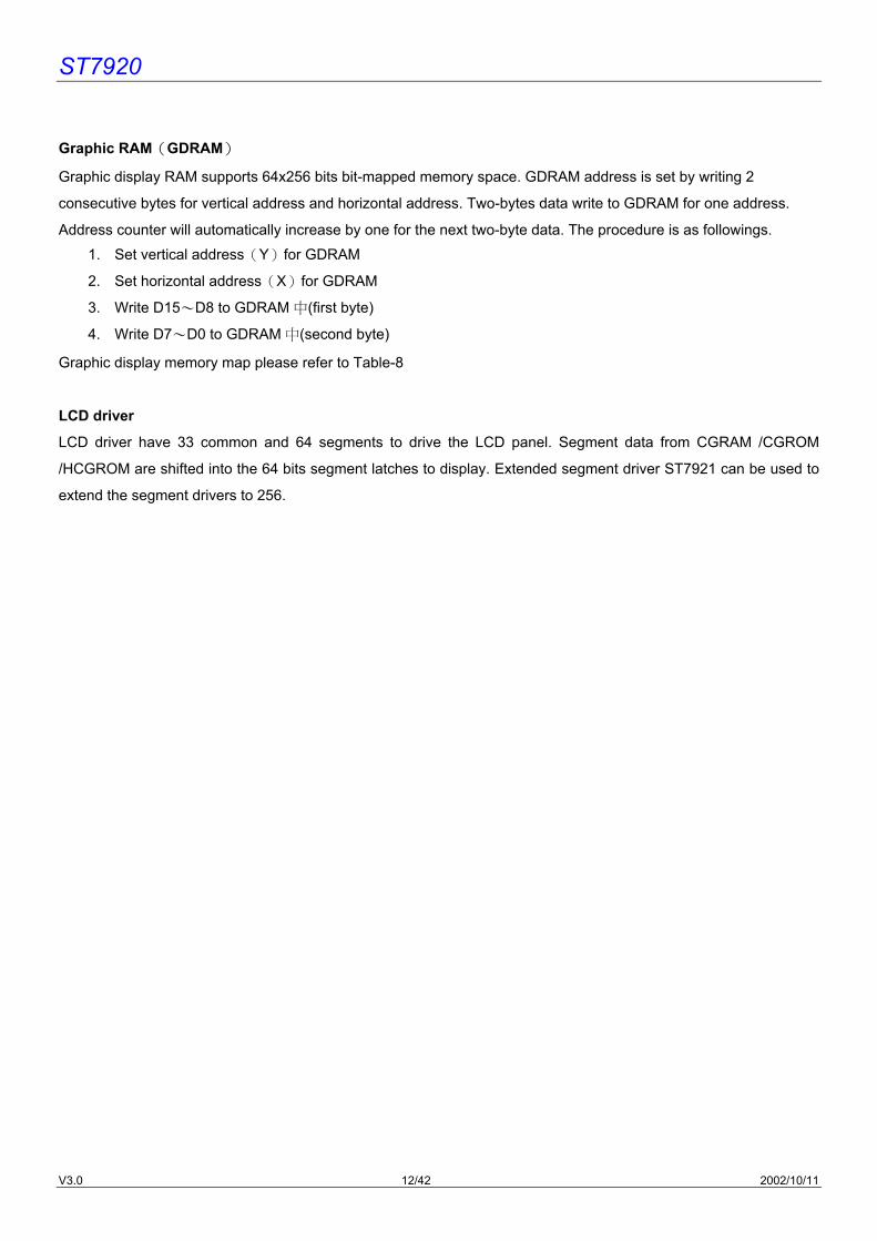
V3.0 13/42 2002/10/11
DDRAM data (char. code)
CGRAMAddr.
CGRAM data(higher byte)
CGRAM data (lower byte)
B15~ B4 B3
B2
B1
B0
B5
B4
B3
B2
B1
B0
D15
D14
D13
D12
D11
D10
D9
D8
D7
D6
D5
D4
D3
D2
D1
D0
0 0 0 0 0 0 0 0 0 1 0 0 0 1 1 0 0 0 0 0 0 0 0 1 1 1 1 1 1 1 1 0 0 1 0 0 0 0 0 0 0 0 1 0 0 0 0 1 0 0 0 0 0 1 0 0 0 1 0 0 0 0 1 1 0 0 0 1 0 0 0 0 0 1 1 1 1 1 1 0 0 1 0 0 0 0 1 0 0 1 0 0 1 0 0 0 0 1 0 0 0 1 0 1 0 0 1 1 1 1 0 0 1 0 0 0 0 1 0 0 0 1 1 0 0 1 1 0 0 1 0 1 0 1 0 0 1 0 0 0 0 1 1 1 1 0 1 0 0 1 1 0 0 1 0 0 1 0 0 0 1 0 0 0 0 0 1 0 0 1 0 0 0 1 0 1 0 0 0 0 1 0 0 1 0 0 1 0 0 1 0 0 0 0 0 1 0 0 0 0 1 0 1 0 0 0 1 0 0 1 0 0 0 0 1 0 0 0 0 0 1 0 1 1 0 0 1 1 1 1 0 0 0 0 1 0 0 0 0 0 1 1 0 0 0 0 1 0 0 1 0 0 0 1 0 0 0 0 0 0 1 1 0 1 0 0 0 0 0 0 0 0 1 0 0 0 0 0 0 0 1 1 1 0 0 0 0 0 0 0 0 1 0 0 0 0 0 0 0 0
0 X 00 X 00
1 1 1 1 0 0 0 0 0 0 0 0 0 0 0 0 0 0 0 0 0 0 0 0 0 0 0 0 1 1 0 0 0 0 0 0 0 1 1 0 0 0 0 1 0 0 0 1 1 0 1 0 0 0 0 0 0 1 0 0 0 0 1 0 0 0 1 0 0 0 0 1 0 0 1 1 0 1 0 0 0 0 1 1 0 1 0 1 1 1 0 1 1 0 1 0 0 1 0 0 0 1 0 0 1 0 0 0 0 0 0 0 1 0 1 0 0 1 0 0 0 1 0 1 0 1 1 1 1 1 1 1 0 0 1 0 0 1 0 0 0 1 1 0 0 1 0 0 0 0 0 1 0 0 1 0 0 1 0 0 0 1 1 1 0 1 1 1 1 1 1 1 0 0 1 0 0 1 0 0 1 0 0 0 0 1 0 0 0 0 0 1 0 0 1 0 0 1 0 0 1 0 0 1 0 1 1 1 1 1 1 1 0 0 1 0 0 1 0 0 1 0 1 0 0 1 0 0 0 0 0 0 0 0 1 0 0 1 0 0 1 0 1 1 0 1 1 1 1 1 1 1 1 0 0 0 1 0 0 1 1 0 0 1 0 1 0 0 0 0 0 1 0 1 0 0 1 0 0 1 1 0 1 1 0 1 1 1 1 1 1 1 0 0 1 1 1 0 0 1 1 1 0 1 0 1 0 0 0 0 0 1 0 0 0 1 0 0 0
0 X 01 X 01
1 1 1 1 0 0 0 0 0 0 0 0 0 0 0 0 0 0 0 0
Table 5: DDRAM data(character code), CGRAM data / address map Note:
1. DDRAM data (character code) bit1 and bit2 are the same as CGRAM address bit4 and bit5.
2. CGRAM address bit0 to bit3 specify total 16 rows. Row16 is for cursor display. The data in row 16 will be logical OR to
the cursor.
3. CGRAM data for each address is 16 bits.
4. DDRAM data to select CGRAM bit4 to bit15 must be “0”. Bit0 and bit3 value are “don’t care”.
ST7920
V3.0 14/42 2002/10/11
ICON RAM data ICON RAM address
Set SR ”0”, and then set IRAM address AC3….AC0 Higher byte Lower byte
AC3 AC2 AC1 AC0 D15 D14 D13 D12 D11 D10 D9 D8 D7 D6 D5 D4 D3 D2 D1 D00 0 0 0 SEG0 SEG1 SEG2 SEG3 SEG4 SEG5 SEG6 SEG7 SEG8 SEG9 SEG10 SEG11 SEG12 SEG13 SEG14 SEG15
0 0 0 1 SEG16 SEG17 SEG18 SEG19 SEG20 SEG21 SEG22 SEG23 SEG24 SEG25 SEG26 SEG27 SEG28 SEG29 SEG30 SEG31
0 0 1 0 SEG32 SEG33 SEG34 SEG35 SEG36 SEG37 SEG38 SEG39 SEG40 SEG41 SEG42 SEG43 SEG44 SEG45 SEG46 SEG47
0 0 1 1 SEG48 SEG49 SEG50 SEG51 SEG52 SEG53 SEG54 SEG55 SEG56 SEG57 SEG58 SEG59 SEG60 SEG61 SEG62 SEG63
0 1 0 0 SEG64 SEG65 SEG66 SEG67 SEG68 SEG69 SEG70 SEG71 SEG72 SEG73 SEG74 SEG75 SEG76 SEG77 SEG78 SEG79
0 1 0 1 SEG80 SEG81 SEG82 SEG83 SEG84 SEG85 SEG86 SEG87 SEG88 SEG89 SEG90 SEG91 SEG92 SEG93 SEG94 SEG95
0 1 1 0 SEG96 SEG97 SEG98 SEG99 SEG100 SEG101 SEG102 SEG103 SEG104 SEG105 SEG106 SEG107 SEG108 SEG109 SEG110 SEG111
0 1 1 1 SEG112 SEG113 SEG114 SEG115 SEG116 SEG117 SEG118 SEG119 SEG120 SEG121 SEG122 SEG123 SEG124 SEG125 SEG126 SEG127
1 0 0 0 SEG128 SEG129 SEG130 SEG131 SEG132 SEG133 SEG134 SEG135 SEG136 SEG137 SEG138 SEG139 SEG140 SEG141 SEG142 SEG143
1 0 0 1 SEG144 SEG145 SEG146 SEG147 SEG148 SEG149 SEG150 SEG151 SEG152 SEG153 SEG154 SEG155 SEG156 SEG157 SEG158 SEG159
1 0 1 0 SEG160 SEG161 SEG162 SEG163 SEG164 SEG165 SEG166 SEG167 SEG168 SEG169 SEG170 SEG171 SEG172 SEG173 SEG174 SEG175
1 0 1 1 SEG176 SEG177 SEG178 SEG179 SEG180 SEG181 SEG182 SEG183 SEG184 SEG185 SEG186 SEG187 SEG188 SEG189 SEG190 SEG191
1 1 0 0 SEG192 SEG193 SEG194 SEG195 SEG196 SEG197 SEG198 SEG199 SEG200 SEG201 SEG202 SEG203 SEG204 SEG205 SEG206 SEG207
1 1 0 1 SEG208 SEG209 SEG210 SEG211 SEG212 SEG213 SEG214 SEG215 SEG216 SEG217 SEG218 SEG219 SEG220 SEG221 SEG222 SEG223
1 1 1 0 SEG224 SEG225 SEG226 SEG227 SEG228 SEG229 SEG230 SEG231 SEG232 SEG233 SEG234 SEG235 SEG236 SEG237 SEG238 SEG239
1 1 1 1 --- --- --- --- --- --- --- --- --- --- --- --- --- --- --- ---
Table 6 ICON RAM address, data and Segment pins
Table 7 16x8 half-height characters
ST7920
V3.0 15/42 2002/10/11
Table 8 GDRAM display coordinates and corresponding address
GDRAM Horizontal address(X)
GD
RA
M V
ertical address
︵Y
︶
0 151 ...........0123456789
101112131415161718192021222324252627282930313233343536373839404142434445464748495051525354555657585960616263
...........
...........
...........b14b15 b0b13
ST7920
V3.0 16/42 2002/10/11
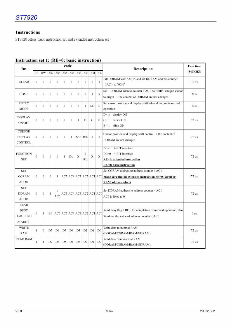
Instructions ST7920 offers basic instruction set and extended instruction set:
Instruction set 1: (RE=0: basic instruction) code
Ins RS RW DB7 DB6 DB5 DB4 DB3 DB2 DB1 DB0
Description Exec time
(540KHZ)
CLEAR 0 0 0 0 0 0 0 0 0 1Fill DDRAM with "20H", and set DDRAM address counter
(AC)to "00H" 1.6 ms
HOME 0 0 0 0 0 0 0 0 1 XSet DDRAM address counter(AC)to "00H", and put cursor
to origin ;the content of DDRAM are not changed 72us
ENTRY
MODE 0 0 0 0 0 0 0 1 I/D S
Set cursor position and display shift when doing write or read
operation 72us
DISPLAY
ON/OFF 0 0 0 0 0 0 1 D C B
D=1: display ON
C=1: cursor ON
B=1: blink ON
72 us
CURSOR
DISPLAY
CONTROL
0 0 0 0 0 1 S/C R/L X XCursor position and display shift control ;the content of
DDRAM are not changed 72 us
FUNCTION
SET 0 0 0 0 1 DL X
0
RE X X
DL=1 8-BIT interface
DL=0 4-BIT interface
RE=1: extended instruction
RE=0: basic instruction
72 us
SET
CGRAM
ADDR.
0 0 0 1 AC5 AC4 AC3 AC2 AC1 AC0
Set CGRAM address to address counter(AC)
Make sure that in extended instruction SR=0 (scroll or
RAM address select)
72 us
SET
DDRAM
ADDR.
0 0 1 0
AC6 AC5 AC4 AC3 AC2 AC1 AC0
Set DDRAM address to address counter(AC)
AC6 is fixed to 0 72 us
READ
BUSY
FLAG(BF)
& ADDR.
0 1 BF AC6 AC5 AC4 AC3 AC2 AC1 AC0Read busy flag(BF)for completion of internal operation, also
Read out the value of address counter(AC) 0 us
WRITE
RAM 1 0 D7 D6 D5 D4 D3 D2 D1 D0
Write data to internal RAM
(DDRAM/CGRAM/IRAM/GDRAM) 72 us
READ RAM
1 1 D7 D6 D5 D4 D3 D2 D1 D0
Read data from internal RAM
(DDRAM/CGRAM/IRAM/GDRAM) 72 us
ST7920
V3.0 17/42 2002/10/11
Instruction set 2: (RE=1: extended instruction) code
Inst. RS RW DB7 DB6 DB5 DB4 DB3 DB2 DB1 DB0
description Exec. time
(540KHZ)
STAND BY 0 0 0 0 0 0 0 0 0 1Enter stand by mode, any other instruction can terminate
(Com1..32 halted, only Com33 ICON can display) 72 us
SCROLL or
RAM
ADDR.
SELECT
0 0 0 0 0 0 0 0 1 SR
SR=1: enable vertical scroll position
SR=0: enable IRAM address (extended instruction)
SR=0: enable CGRAM address(basic instruction)
72 us
REVERSE 0 0 0 0 0 0 0 1 R1 R0
Select 1 out of 4 line ( in DDRAM) and decide whether to
reverse the display by toggling this instruction
R1,R0 initial value is 00
72 us
EXTENDED
FUNCTION
SET
0 0 0 0 1 DL X 1
RE G 0
DL=1 8-BIT interface
DL=0 4-BIT interface
RE=1: extended instruction set
RE=0: basic instruction set
G=1 :graphic display ON
G=0 :graphic display OFF
72 us
SET
IRAM or
SCROLL
ADDR
0 0 0 1 AC5 AC4 AC3 AC2 AC1 AC0SR=1: AC5~AC0 the address of vertical scroll
SR=0: AC3~AC0 the address of ICON RAM 72 us
SET
GRAPHIC
RAM
ADDR.
0 0 1 0
AC6
0
AC5
0
AC4
AC3
AC3
AC2
AC2
AC1
AC1
AC0
AC0
Set GDRAM address to address counter(AC)
First set vertical address and the horizontal address by
consecutive writing
Vertical address range AC6...AC0
Horizontal address range AC3…AC0
72 us
Note:
1. Make sure that ST7920 is not in busy state by reading the busy flag before sending instruction or data. If use delay loop
instead please make sure the delay time is enough. Please refer to the instruction execution time.
2. “RE”is the selection bit of basic and extended instruction set. Each time when altering the value of RE it will remain.
There is no need to set RE every time when using the same group of instruction set.
ST7920
V3.0 18/42 2002/10/11
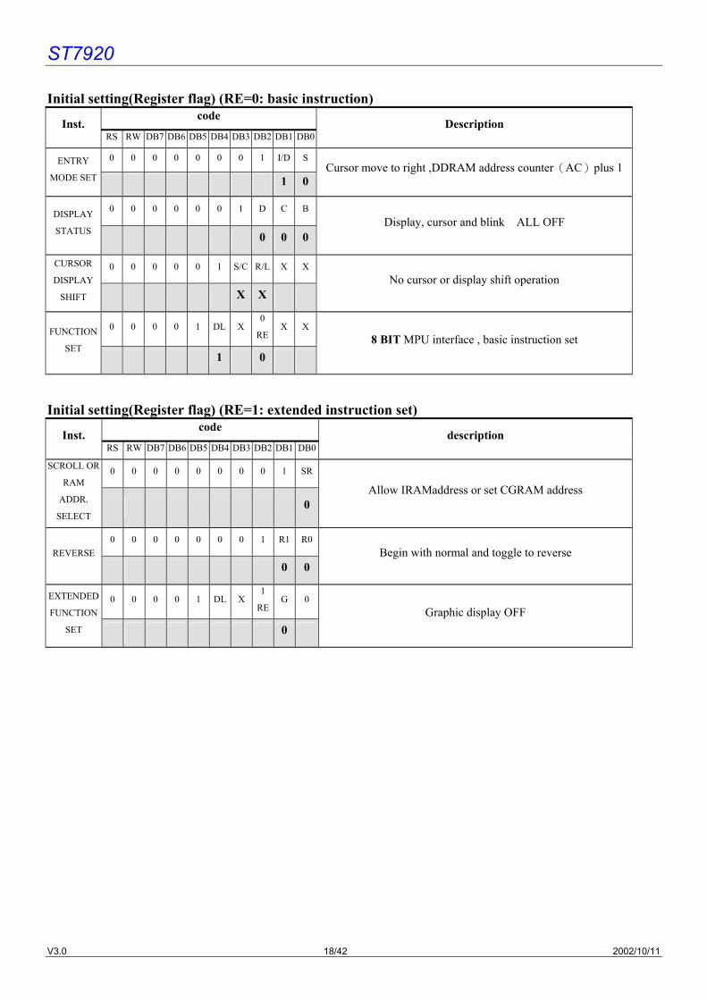
Initial setting(Register flag) (RE=0: basic instruction) code
Inst. RS RW DB7 DB6 DB5 DB4 DB3 DB2 DB1 DB0
Description
0 0 0 0 0 0 0 1 I/D SENTRY
MODE SET 1 0Cursor move to right ,DDRAM address counter(AC)plus 1
0 0 0 0 0 0 1 D C BDISPLAY
STATUS 0 0 0Display, cursor and blink ALL OFF
0 0 0 0 0 1 S/C R/L X XCURSOR
DISPLAY
SHIFT X X No cursor or display shift operation
0 0 0 0 1 DL X 0
RE X XFUNCTION
SET 1 0
8 BIT MPU interface , basic instruction set
Initial setting(Register flag) (RE=1: extended instruction set) code
Inst. RS RW DB7 DB6 DB5 DB4 DB3 DB2 DB1 DB0
description
0 0 0 0 0 0 0 0 1 SRSCROLL OR
RAM
ADDR.
SELECT 0
Allow IRAMaddress or set CGRAM address
0 0 0 0 0 0 0 1 R1 R0REVERSE
0 0Begin with normal and toggle to reverse
0 0 0 0 1 DL X 1
RE G 0EXTENDED
FUNCTION
SET 0 Graphic display OFF
ST7920
V3.0 19/42 2002/10/11
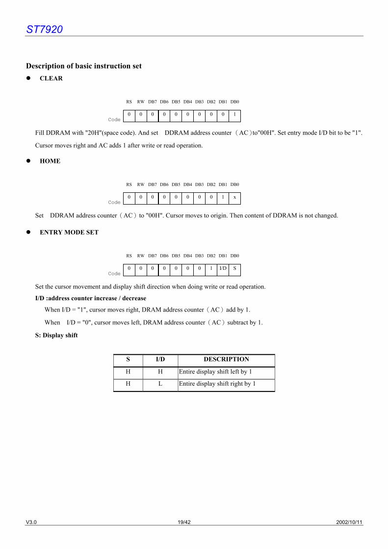
Description of basic instruction set CLEAR
Fill DDRAM with "20H"(space code). And set DDRAM address counter (AC)to"00H". Set entry mode I/D bit to be "1".
Cursor moves right and AC adds 1 after write or read operation.
HOME
Set DDRAM address counter(AC)to "00H". Cursor moves to origin. Then content of DDRAM is not changed.
ENTRY MODE SET
Set the cursor movement and display shift direction when doing write or read operation.
I/D :address counter increase / decrease
When I/D = "1", cursor moves right, DRAM address counter(AC)add by 1.
When I/D = "0", cursor moves left, DRAM address counter(AC)subtract by 1.
S: Display shift
S I/D DESCRIPTION
H H Entire display shift left by 1
H L Entire display shift right by 1
0
0
0
0
0
0
0
0
0
0
0
0
0
0
0
0
0
0
0
0
0
0
0
1
Code
Code
Code
RS
RS
RS
RW
RW
RW
DB7
DB7
DB7
DB6
DB6
DB6
DB5
DB5
DB5
DB4
DB4
DB4
DB1
DB1
DB1
DB2
DB2
DB2
DB3
DB3
DB3
0
1
I/D
1
x
S
DB0
DB0
DB0
ST7920
V3.0 20/42 2002/10/11
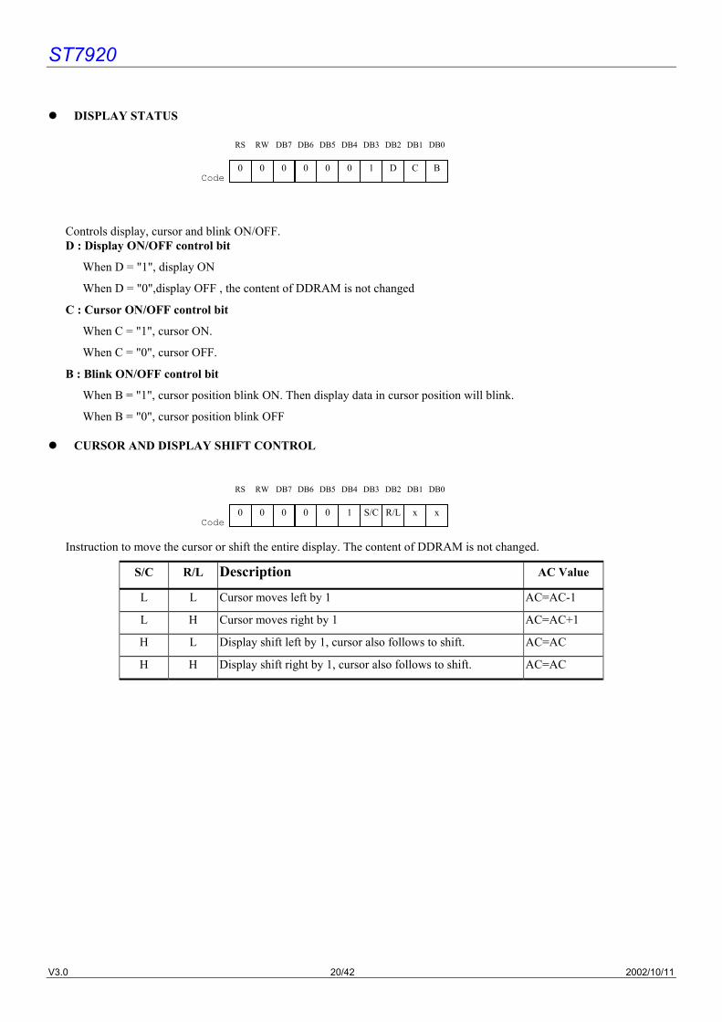
DISPLAY STATUS
Controls display, cursor and blink ON/OFF. D : Display ON/OFF control bit
When D = "1", display ON
When D = "0",display OFF , the content of DDRAM is not changed
C : Cursor ON/OFF control bit
When C = "1", cursor ON.
When C = "0", cursor OFF.
B : Blink ON/OFF control bit
When B = "1", cursor position blink ON. Then display data in cursor position will blink.
When B = "0", cursor position blink OFF
CURSOR AND DISPLAY SHIFT CONTROL
Instruction to move the cursor or shift the entire display. The content of DDRAM is not changed.
S/C R/L Description AC Value
L L Cursor moves left by 1 AC=AC-1
L H Cursor moves right by 1 AC=AC+1
H L Display shift left by 1, cursor also follows to shift. AC=AC
H H Display shift right by 1, cursor also follows to shift. AC=AC
0
0
0
0
0
0
0
0
0
0
0
1
1
S/C
D
R/L
Code
Code
RS
RS
RW
RW
DB7
DB7
DB6
DB6
DB5
DB5
DB4
DB4
DB1
DB1
DB2
DB2
DB3
DB3
C
x
B
x
DB0
DB0
ST7920
V3.0 21/42 2002/10/11
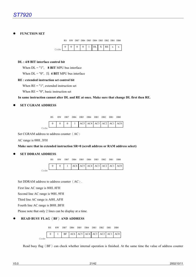
FUNCTION SET
DL : 4/8 BIT interface control bit
When DL = "1", 8 BIT MPU bus interface
When DL = "0", 為 4 BIT MPU bus interface
RE : extended instruction set control bit
When RE = "1", extended instruction set
When RE = "0", basic instruction set
In same instruction cannot alter DL and RE at once. Make sure that change DL first then RE.
SET CGRAM ADDRESS
Set CGRAM address to address counter(AC)
AC range is 00H..3FH
Make sure that in extended instruction SR=0 (scroll address or RAM address select)
SET DDRAM ADDRESS
Set DDRAM address to address counter(AC).
First line AC range is 80H..8FH
Second line AC range is 90H..9FH
Third line AC range is A0H..AFH
Fourth line AC range is B0H..BFH
Please note that only 2 lines can be display at a time.
READ BUSY FLAG(BF)AND ADDRESS
Read busy flag(BF)can check whether internal operation is finished. At the same time the value of address counter
0 0 0 0 1 DL X RECode
RS RW DB7 DB6 DB5 DB4 DB1DB2DB3
x x
DB0
0 0 0 1 AC5 AC4 AC3 AC2
Code
RS RW DB7 DB6 DB5 DB4 DB1DB2DB3
AC1 AC0
DB0
0 0 1 AC6 AC5 AC4 AC3 AC2
Code
RS RW DB7 DB6 DB5 DB4 DB1DB2DB3
AC1 AC0
DB0
0 1 BF AC6 AC5 AC4 AC3 AC2
Code
RS RW DB7 DB6 DB5 DB4 DB1DB2DB3
AC1 AC0
DB0
ST7920
V3.0 22/42 2002/10/11
(AC)is also read. When BF = “1” new instruction will not be accepted. Must wait for BF = “0” for new instruction.
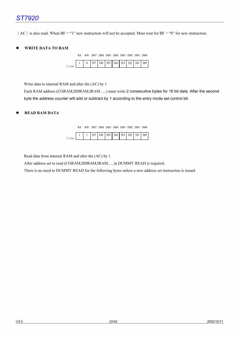
WRITE DATA TO RAM
Write data to internal RAM and alter the (AC) by 1
Each RAM address (CGRAM,DDRAM,IRAM…..) must write 2 consecutive bytes for 16 bit data. After the second
byte the address counter will add or subtract by 1 according to the entry mode set control bit.
READ RAM DATA
Read data from internal RAM and alter the (AC) by 1
After address set to read (CGRAM,DDRAM,IRAM…..)a DUMMY READ is required.
There is no need to DUMMY READ for the following bytes unless a new address set instruction is issued.
1
1
0
1
D7
D7
D6
D6
D5
D5
D4
D4
D3
D3
D2
D2
Code
Code
RS
RS
RW
RW
DB7
DB7
DB6
DB6
DB5
DB5
DB4
DB4
DB1
DB1
DB2
DB2
DB3
DB3
D1
D1
D0
D0
DB0
DB0
ST7920
V3.0 23/42 2002/10/11
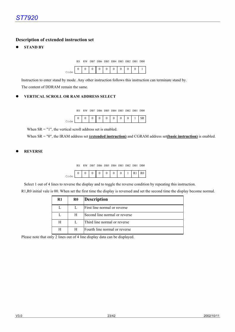
Description of extended instruction set STAND BY
Instruction to enter stand by mode. Any other instruction follows this instruction can terminate stand by.
The content of DDRAM remain the same.
VERTICAL SCROLL OR RAM ADDRESS SELECT
When SR = "1", the vertical scroll address set is enabled.
When SR = "0", the IRAM address set (extended instruction) and CGRAM address set(basic instruction) is enabled.
REVERSE
Select 1 out of 4 lines to reverse the display and to toggle the reverse condition by repeating this instruction.
R1,R0 initial vale is 00. When set the first time the display is reversed and set the second time the display become normal.
R1 R0 Description
L L First line normal or reverse
L H Second line normal or reverse
H L Third line normal or reverse
H H Fourth line normal or reverse
Please note that only 2 lines out of 4 line display data can be displayed.
0
0
0
0
0
0
0
0
0
0
0
0
0
0
0
0
0
0
0
0
0
0
0
1
Code
Code
Code
RS
RS
RS
RW
RW
RW
DB7
DB7
DB7
DB6
DB6
DB6
DB5
DB5
DB5
DB4
DB4
DB4
DB1
DB1
DB1
DB2
DB2
DB2
DB3
DB3
DB3
0
1
R1
1
SR
R0
DB0
DB0
DB0
ST7920
V3.0 24/42 2002/10/11
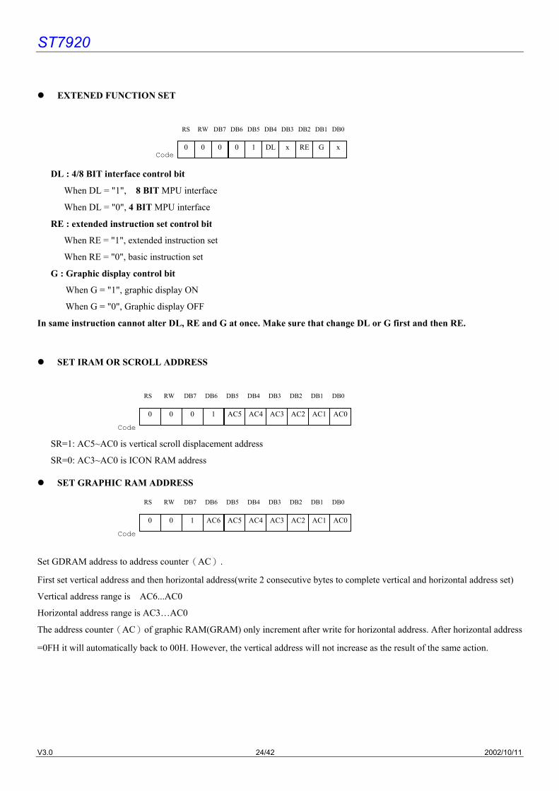
EXTENED FUNCTION SET
DL : 4/8 BIT interface control bit
When DL = "1", 8 BIT MPU interface
When DL = "0", 4 BIT MPU interface
RE : extended instruction set control bit
When RE = "1", extended instruction set
When RE = "0", basic instruction set
G : Graphic display control bit
When G = "1", graphic display ON
When G = "0", Graphic display OFF
In same instruction cannot alter DL, RE and G at once. Make sure that change DL or G first and then RE.
SET IRAM OR SCROLL ADDRESS
SR=1: AC5~AC0 is vertical scroll displacement address
SR=0: AC3~AC0 is ICON RAM address
SET GRAPHIC RAM ADDRESS
Set GDRAM address to address counter(AC).
First set vertical address and then horizontal address(write 2 consecutive bytes to complete vertical and horizontal address set)
Vertical address range is AC6...AC0
Horizontal address range is AC3…AC0
The address counter(AC)of graphic RAM(GRAM) only increment after write for horizontal address. After horizontal address
=0FH it will automatically back to 00H. However, the vertical address will not increase as the result of the same action.
0 0 0 0 1 DL x RECode
RS RW DB7 DB6 DB5 DB4 DB1DB2DB3
G x
DB0
0 0 1 AC6 AC5 AC4 AC3 AC2
Code
RS RW DB7 DB6 DB5 DB4 DB1DB2DB3
AC1 AC0
DB0
0 0 0 1 AC5 AC4 AC3 AC2
Code
RS RW DB7 DB6 DB5 DB4 DB1DB2DB3
AC1 AC0
DB0
ST7920
V3.0 25/42 2002/10/11
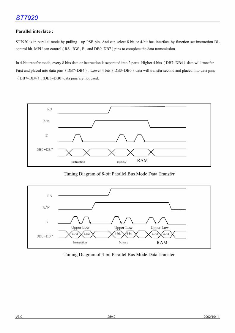
Parallel interface : ST7920 is in parallel mode by pulling up PSB pin. And can select 8 bit or 4-bit bus interface by function set instruction DL
control bit. MPU can control ( RS , RW , E , and DB0..DB7 ) pins to complete the data transmission.
In 4-bit transfer mode, every 8 bits data or instruction is separated into 2 parts. Higher 4 bits(DB7~DB4)data will transfer
First and placed into data pins(DB7~DB4). Lower 4 bits(DB3~DB0)data will transfer second and placed into data pins
(DB7~DB4). (DB3~DB0) data pins are not used.
DB0-DB7
R/W
RS
E
DummyInstruction RAM
Timing Diagram of 8-bit Parallel Bus Mode Data Transfer
DB0-DB7
R/W
RS
E
Dummy RAM
Timing Diagram of 4-bit Parallel Bus Mode Data Transfer
Instruction
4-bit 4-bit 4-bit 4-bit 4-bit 4-bit
Upper Low Upper Low Upper Low
ST7920
V3.0 26/42 2002/10/11
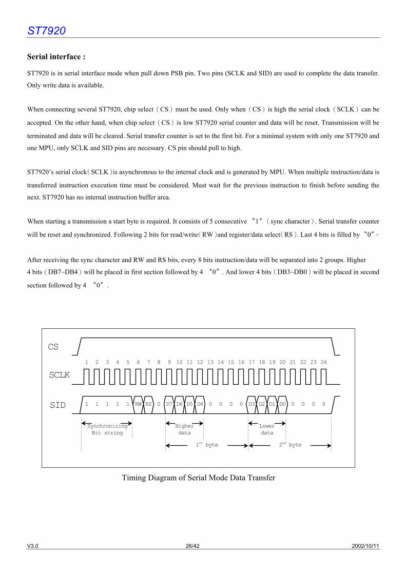
Serial interface : ST7920 is in serial interface mode when pull down PSB pin. Two pins (SCLK and SID) are used to complete the data transfer.
Only write data is available.
When connecting several ST7920, chip select(CS)must be used. Only when(CS)is high the serial clock(SCLK)can be
accepted. On the other hand, when chip select(CS)is low ST7920 serial counter and data will be reset. Transmission will be
terminated and data will be cleared. Serial transfer counter is set to the first bit. For a minimal system with only one ST7920 and
one MPU, only SCLK and SID pins are necessary. CS pin should pull to high.
ST7920’s serial clock(SCLK)is asynchronous to the internal clock and is generated by MPU. When multiple instruction/data is
transferred instruction execution time must be considered. Must wait for the previous instruction to finish before sending the
next. ST7920 has no internal instruction buffer area.
When starting a transmission a start byte is required. It consists of 5 consecutive 〝1〞(sync character). Serial transfer counter
will be reset and synchronized. Following 2 bits for read/write(RW)and register/data select(RS). Last 4 bits is filled by 〝0〞。
After receiving the sync character and RW and RS bits, every 8 bits instruction/data will be separated into 2 groups. Higher
4 bits(DB7~DB4)will be placed in first section followed by 4 〝0〞. And lower 4 bits(DB3~DB0)will be placed in second
section followed by 4 〝0〞.
1 2 4 5 6 7 8 9 10 11 12 13 14 15 16 17 18 19 20 21 22 23 24
1 1 1 1 1 RW RS 0 D7 D6 D5 D4 0 0 0 0 0 0 0 0D3 D2 D1 D0
CS
SCLK
SID
SynchronizingBit string
Higherdata
Lowerdata
3
1st byte 2nd byte
Timing Diagram of Serial Mode Data Transfer
ST7920
V3.0 27/42 2002/10/11
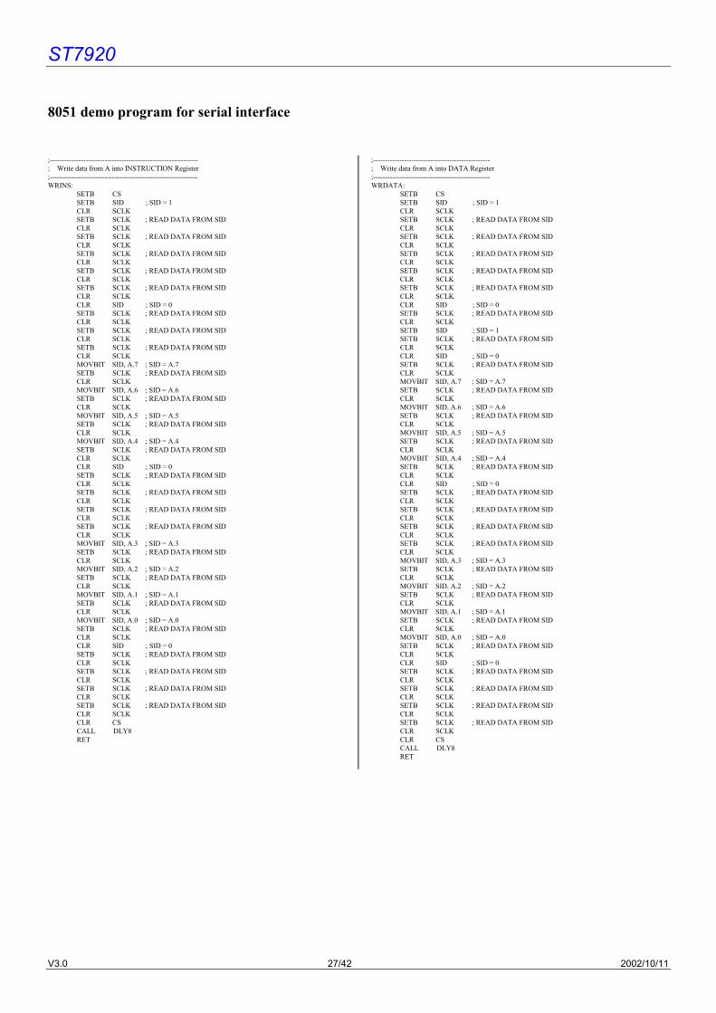
8051 demo program for serial interface ;-------------------------------------------------------------- ; Write data from A into INSTRUCTION Register ;-------------------------------------------------------------- WRINS: SETB CS SETB SID ; SID = 1 CLR SCLK SETB SCLK ; READ DATA FROM SID CLR SCLK SETB SCLK ; READ DATA FROM SID CLR SCLK SETB SCLK ; READ DATA FROM SID CLR SCLK SETB SCLK ; READ DATA FROM SID CLR SCLK SETB SCLK ; READ DATA FROM SID CLR SCLK CLR SID ; SID = 0 SETB SCLK ; READ DATA FROM SID CLR SCLK SETB SCLK ; READ DATA FROM SID CLR SCLK SETB SCLK ; READ DATA FROM SID CLR SCLK MOVBIT SID, A.7 ; SID = A.7 SETB SCLK ; READ DATA FROM SID CLR SCLK MOVBIT SID, A.6 ; SID = A.6 SETB SCLK ; READ DATA FROM SID CLR SCLK MOVBIT SID, A.5 ; SID = A.5 SETB SCLK ; READ DATA FROM SID CLR SCLK MOVBIT SID, A.4 ; SID = A.4 SETB SCLK ; READ DATA FROM SID CLR SCLK CLR SID ; SID = 0 SETB SCLK ; READ DATA FROM SID CLR SCLK SETB SCLK ; READ DATA FROM SID CLR SCLK SETB SCLK ; READ DATA FROM SID CLR SCLK SETB SCLK ; READ DATA FROM SID CLR SCLK MOVBIT SID, A.3 ; SID = A.3 SETB SCLK ; READ DATA FROM SID CLR SCLK MOVBIT SID, A.2 ; SID = A.2 SETB SCLK ; READ DATA FROM SID CLR SCLK MOVBIT SID, A.1 ; SID = A.1 SETB SCLK ; READ DATA FROM SID CLR SCLK MOVBIT SID, A.0 ; SID = A.0 SETB SCLK ; READ DATA FROM SID CLR SCLK CLR SID ; SID = 0 SETB SCLK ; READ DATA FROM SID CLR SCLK SETB SCLK ; READ DATA FROM SID CLR SCLK SETB SCLK ; READ DATA FROM SID CLR SCLK SETB SCLK ; READ DATA FROM SID CLR SCLK CLR CS CALL DLY8 RET
;------------------------------------------------- ; Write data from A into DATA Register ;------------------------------------------------- WRDATA: SETB CS SETB SID ; SID = 1 CLR SCLK SETB SCLK ; READ DATA FROM SID CLR SCLK SETB SCLK ; READ DATA FROM SID CLR SCLK SETB SCLK ; READ DATA FROM SID CLR SCLK SETB SCLK ; READ DATA FROM SID CLR SCLK SETB SCLK ; READ DATA FROM SID CLR SCLK CLR SID ; SID = 0 SETB SCLK ; READ DATA FROM SID CLR SCLK SETB SID ; SID = 1 SETB SCLK ; READ DATA FROM SID CLR SCLK CLR SID ; SID = 0 SETB SCLK ; READ DATA FROM SID CLR SCLK MOVBIT SID, A.7 ; SID = A.7 SETB SCLK ; READ DATA FROM SID CLR SCLK MOVBIT SID, A.6 ; SID = A.6 SETB SCLK ; READ DATA FROM SID CLR SCLK MOVBIT SID, A.5 ; SID = A.5 SETB SCLK ; READ DATA FROM SID CLR SCLK MOVBIT SID, A.4 ; SID = A.4 SETB SCLK ; READ DATA FROM SID CLR SCLK CLR SID ; SID = 0 SETB SCLK ; READ DATA FROM SID CLR SCLK SETB SCLK ; READ DATA FROM SID CLR SCLK SETB SCLK ; READ DATA FROM SID CLR SCLK SETB SCLK ; READ DATA FROM SID CLR SCLK MOVBIT SID, A.3 ; SID = A.3 SETB SCLK ; READ DATA FROM SID CLR SCLK MOVBIT SID, A.2 ; SID = A.2 SETB SCLK ; READ DATA FROM SID CLR SCLK MOVBIT SID, A.1 ; SID = A.1 SETB SCLK ; READ DATA FROM SID CLR SCLK MOVBIT SID, A.0 ; SID = A.0 SETB SCLK ; READ DATA FROM SID CLR SCLK CLR SID ; SID = 0 SETB SCLK ; READ DATA FROM SID CLR SCLK SETB SCLK ; READ DATA FROM SID CLR SCLK SETB SCLK ; READ DATA FROM SID CLR SCLK SETB SCLK ; READ DATA FROM SID CLR SCLK CLR CS CALL DLY8 RET
ST7920
V3.0 28/42 2002/10/11
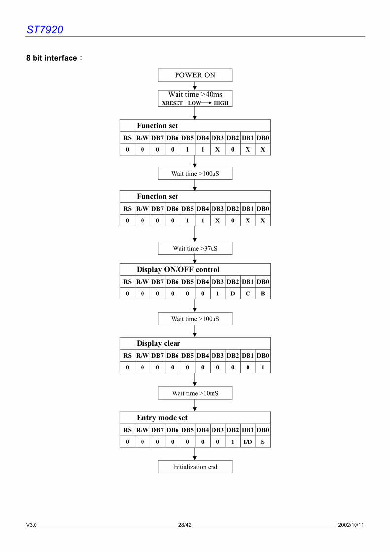
8 bit interface:
POWER ON
Wait time >40msXRESET LOW HIGH
Function set RS R/W DB7 DB6 DB5 DB4 DB3 DB2 DB1 DB0
0 0 0 0 1 1 X 0 X X
Wait time >100uS
Function set RS R/W DB7 DB6 DB5 DB4 DB3 DB2 DB1 DB0
0 0 0 0 1 1 X 0 X X
Wait time >37uS
Display ON/OFF control RS R/W DB7 DB6 DB5 DB4 DB3 DB2 DB1 DB0
0 0 0 0 0 0 1 D C B
Wait time >100uS
Display clear RS R/W DB7 DB6 DB5 DB4 DB3 DB2 DB1 DB0
0 0 0 0 0 0 0 0 0 1
Wait time >10mS
Entry mode set RS R/W DB7 DB6 DB5 DB4 DB3 DB2 DB1 DB0
0 0 0 0 0 0 0 1 I/D S
Initialization end
ST7920
V3.0 29/42 2002/10/11
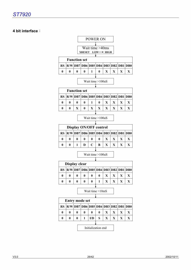
4 bit interface:
POWER ON
Wait time >40msXRESET LOW HIGH
Function set RS R/W DB7 DB6 DB5 DB4 DB3 DB2 DB1 DB0
0 0 0 0 1 0 X X X X
Wait time >100uS
Function set RS R/W DB7 DB6 DB5 DB4 DB3 DB2 DB1 DB0
0 0 0 0 1 0 X X X X
0 0 X 0 X X X X X X
Wait time >100uS
Display ON/OFF control RS R/W DB7 DB6 DB5 DB4 DB3 DB2 DB1 DB0
0 0 0 0 0 0 X X X X
0 0 1 D C B X X X X
Wait time >100uS
Display clear RS R/W DB7 DB6 DB5 DB4 DB3 DB2 DB1 DB0
0 0 0 0 0 0 X X X X
0 0 0 0 0 1 X X X X
Wait time >10mS
Entry mode set RS R/W DB7 DB6 DB5 DB4 DB3 DB2 DB1 DB0
0 0 0 0 0 0 X X X X
0 0 0 1 I/D S X X X X
Initialization end
ST7920
V3.0 30/42 2002/10/11
Built in voltage booster
External reset timing
XRESET pulse width Trw 10us
RESET start time Tres 50ns
Tres
Trw
VDD
XRESET
Vss Cap1M Cap1P Cap2M Cap2P Cap3M Vout
+-
-+
5.4V
Vss
參考電壓
VD2
2.7V
Vout
x
Vout
VDD
VD2
ST7920
V3.0 31/42 2002/10/11
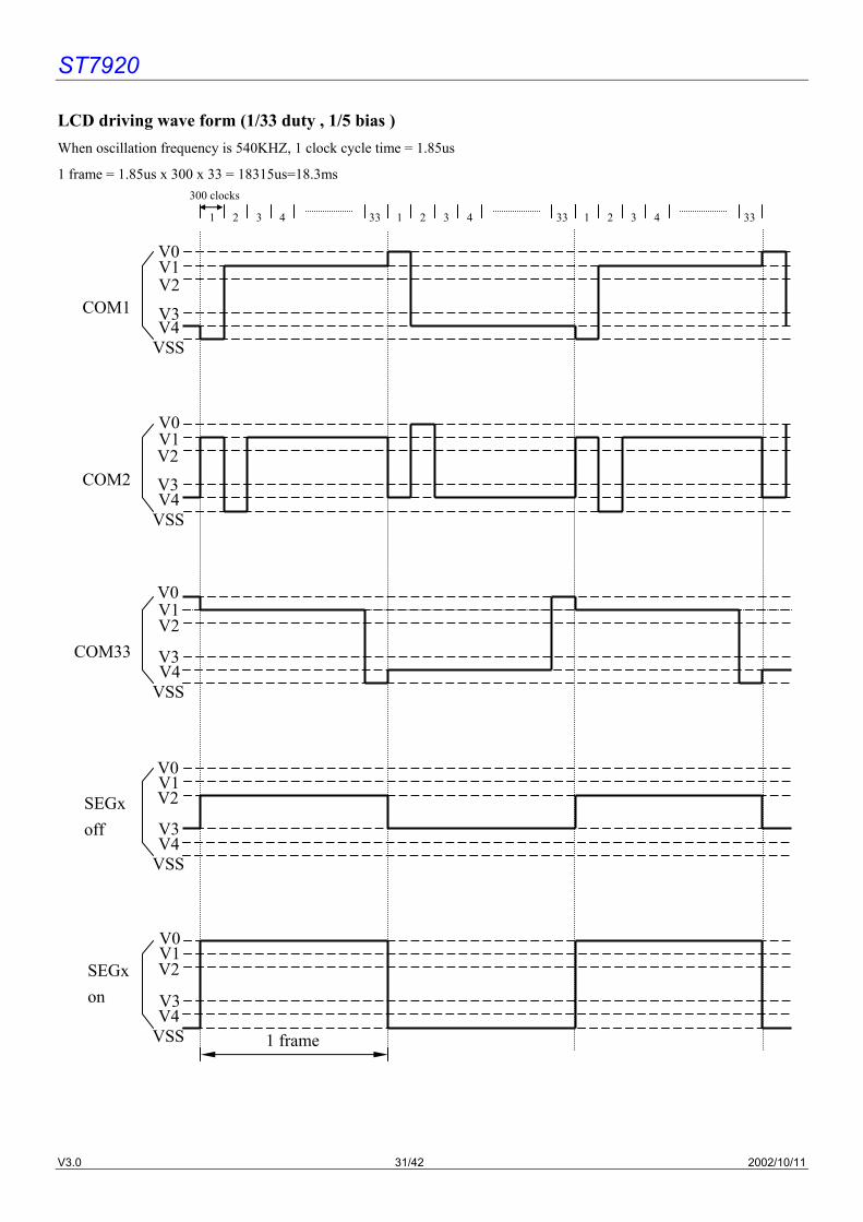
LCD driving wave form (1/33 duty , 1/5 bias ) When oscillation frequency is 540KHZ, 1 clock cycle time = 1.85us
1 frame = 1.85us x 300 x 33 = 18315us=18.3ms
1 2 3 4 33 1 2 3 4 33 1 2 3 4 33
V0 V1 V2
V3 V4
VSS
COM1
V0 V1 V2
V3 V4
VSS
COM2
V0 V1 V2
V3 V4
VSS
COM33
V0 V1 V2
V3 V4
VSS
SEGx off
V0 V1 V2
V3 V4
VSS
SEGx on
1 frame
300 clocks
ST7920
V3.0 32/42 2002/10/11
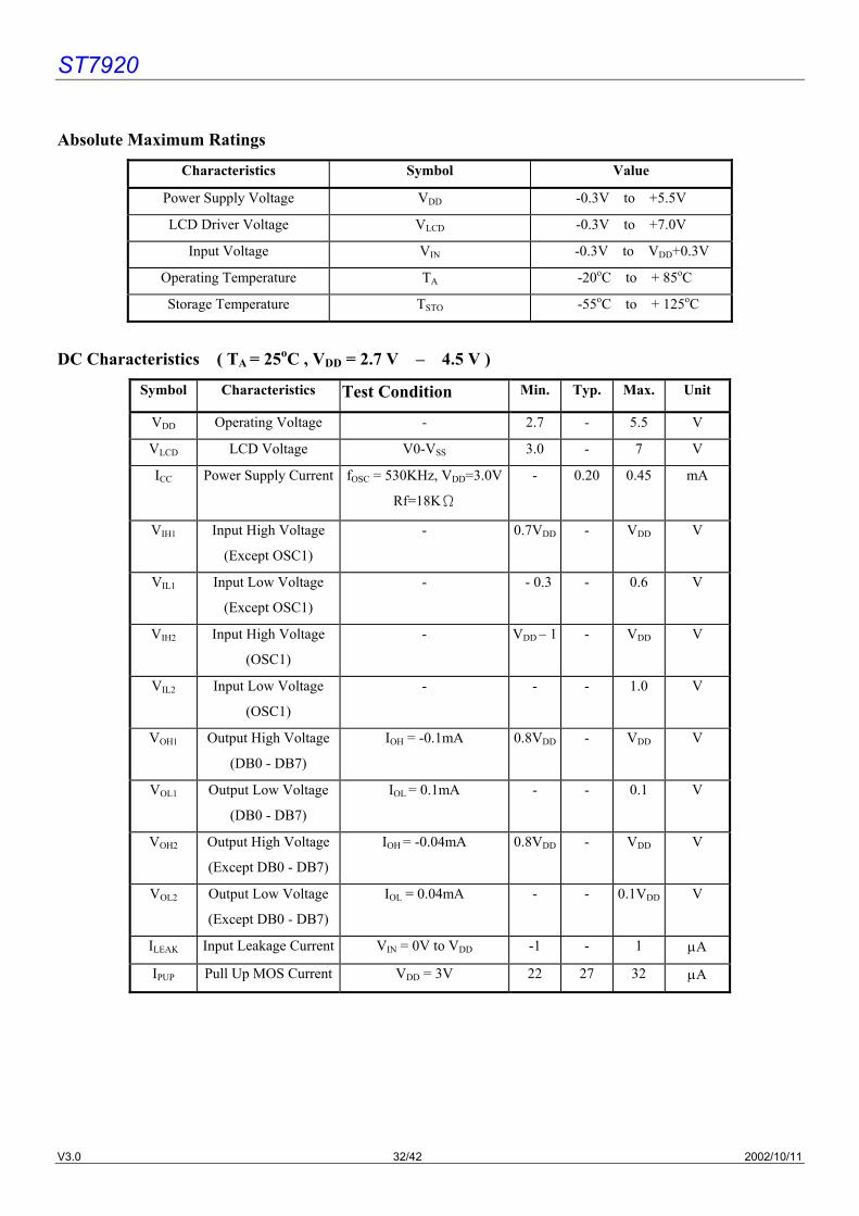
Absolute Maximum Ratings
Characteristics Symbol Value
Power Supply Voltage VDD -0.3V to +5.5V
LCD Driver Voltage VLCD -0.3V to +7.0V
Input Voltage VIN -0.3V to VDD+0.3V
Operating Temperature TA -20oC to + 85oC
Storage Temperature TSTO -55oC to + 125oC
DC Characteristics ( TA = 25oC , VDD = 2.7 V – 4.5 V )
Symbol Characteristics Test Condition Min. Typ. Max. Unit
VDD Operating Voltage - 2.7 - 5.5 V
VLCD LCD Voltage V0-VSS 3.0 - 7 V
ICC Power Supply Current fOSC = 530KHz, VDD=3.0V
Rf=18KΩ
- 0.20 0.45 mA
VIH1 Input High Voltage
(Except OSC1)
- 0.7VDD - VDD V
VIL1 Input Low Voltage
(Except OSC1)
- - 0.3 - 0.6 V
VIH2 Input High Voltage
(OSC1)
- VDD – 1 - VDD V
VIL2 Input Low Voltage
(OSC1)
- - - 1.0 V
VOH1 Output High Voltage
(DB0 - DB7)
IOH = -0.1mA 0.8VDD - VDD V
VOL1 Output Low Voltage
(DB0 - DB7)
IOL = 0.1mA - - 0.1 V
VOH2 Output High Voltage
(Except DB0 - DB7)
IOH = -0.04mA 0.8VDD - VDD V
VOL2 Output Low Voltage
(Except DB0 - DB7)
IOL = 0.04mA - - 0.1VDD V
ILEAK Input Leakage Current VIN = 0V to VDD -1 - 1 µA
IPUP Pull Up MOS Current VDD = 3V 22 27 32 µA
ST7920
V3.0 33/42 2002/10/11
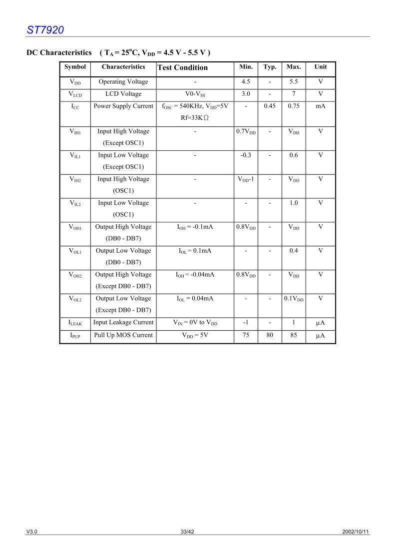
DC Characteristics ( TA = 25oC, VDD = 4.5 V - 5.5 V )
Symbol Characteristics Test Condition Min. Typ. Max. Unit
VDD Operating Voltage - 4.5 - 5.5 V
VLCD LCD Voltage V0-VSS 3.0 - 7 V
ICC Power Supply Current fOSC = 540KHz, VDD=5V
Rf=33KΩ
- 0.45 0.75 mA
VIH1 Input High Voltage
(Except OSC1)
- 0.7VDD - VDD V
VIL1 Input Low Voltage
(Except OSC1)
- -0.3 - 0.6 V
VIH2 Input High Voltage
(OSC1)
- VDD-1 - VDD V
VIL2 Input Low Voltage
(OSC1)
- - - 1.0 V
VOH1 Output High Voltage
(DB0 - DB7)
IOH = -0.1mA 0.8VDD - VDD V
VOL1 Output Low Voltage
(DB0 - DB7)
IOL = 0.1mA - - 0.4 V
VOH2 Output High Voltage
(Except DB0 - DB7)
IOH = -0.04mA 0.8VDD - VDD V
VOL2 Output Low Voltage
(Except DB0 - DB7)
IOL = 0.04mA - - 0.1VDD V
ILEAK Input Leakage Current VIN = 0V to VDD -1 - 1 µA
IPUP Pull Up MOS Current VDD = 5V 75 80 85 µA
ST7920
V3.0 34/42 2002/10/11
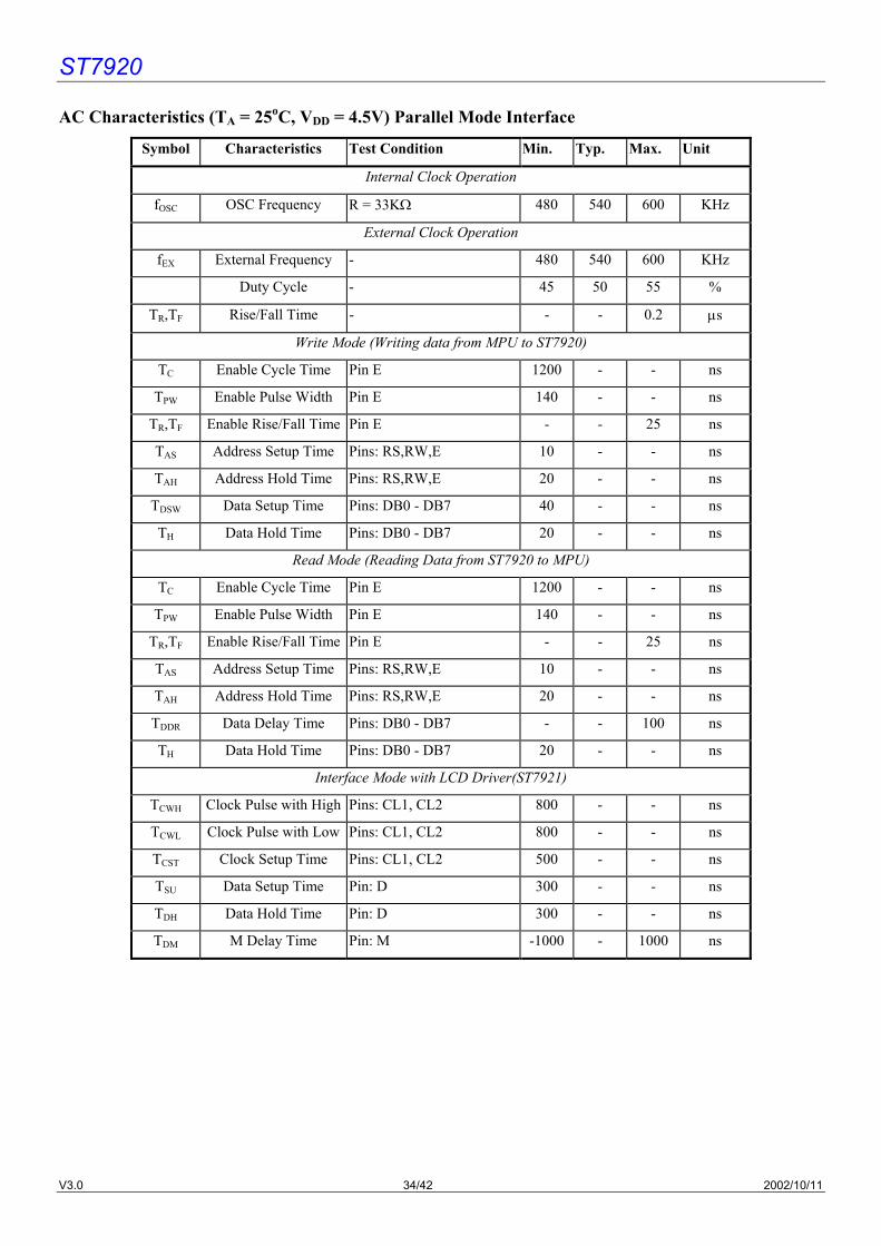
AC Characteristics (TA = 25oC, VDD = 4.5V) Parallel Mode Interface
Symbol Characteristics Test Condition Min. Typ. Max. Unit
Internal Clock Operation
fOSC OSC Frequency R = 33KΩ 480 540 600 KHz
External Clock Operation
fEX External Frequency - 480 540 600 KHz
Duty Cycle - 45 50 55 %
TR,TF Rise/Fall Time - - - 0.2 µs
Write Mode (Writing data from MPU to ST7920)
TC Enable Cycle Time Pin E 1200 - - ns
TPW Enable Pulse Width Pin E 140 - - ns
TR,TF Enable Rise/Fall Time Pin E - - 25 ns
TAS Address Setup Time Pins: RS,RW,E 10 - - ns
TAH Address Hold Time Pins: RS,RW,E 20 - - ns
TDSW Data Setup Time Pins: DB0 - DB7 40 - - ns
TH Data Hold Time Pins: DB0 - DB7 20 - - ns
Read Mode (Reading Data from ST7920 to MPU)
TC Enable Cycle Time Pin E 1200 - - ns
TPW Enable Pulse Width Pin E 140 - - ns
TR,TF Enable Rise/Fall Time Pin E - - 25 ns
TAS Address Setup Time Pins: RS,RW,E 10 - - ns
TAH Address Hold Time Pins: RS,RW,E 20 - - ns
TDDR Data Delay Time Pins: DB0 - DB7 - - 100 ns
TH Data Hold Time Pins: DB0 - DB7 20 - - ns
Interface Mode with LCD Driver(ST7921)
TCWH Clock Pulse with High Pins: CL1, CL2 800 - - ns
TCWL Clock Pulse with Low Pins: CL1, CL2 800 - - ns
TCST Clock Setup Time Pins: CL1, CL2 500 - - ns
TSU Data Setup Time Pin: D 300 - - ns
TDH Data Hold Time Pin: D 300 - - ns
TDM M Delay Time Pin: M -1000 - 1000 ns
ST7920
V3.0 35/42 2002/10/11
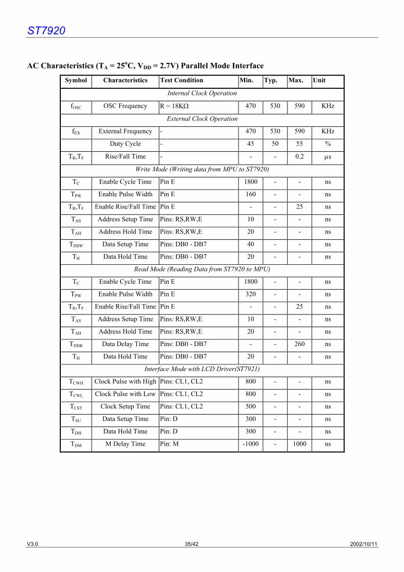
AC Characteristics (TA = 25oC, VDD = 2.7V) Parallel Mode Interface
Symbol Characteristics Test Condition Min. Typ. Max. Unit
Internal Clock Operation
fOSC OSC Frequency R = 18KΩ 470 530 590 KHz
External Clock Operation
fEX External Frequency - 470 530 590 KHz
Duty Cycle - 45 50 55 %
TR,TF Rise/Fall Time - - - 0.2 µs
Write Mode (Writing data from MPU to ST7920)
TC Enable Cycle Time Pin E 1800 - - ns
TPW Enable Pulse Width Pin E 160 - - ns
TR,TF Enable Rise/Fall Time Pin E - - 25 ns
TAS Address Setup Time Pins: RS,RW,E 10 - - ns
TAH Address Hold Time Pins: RS,RW,E 20 - - ns
TDSW Data Setup Time Pins: DB0 - DB7 40 - - ns
TH Data Hold Time Pins: DB0 - DB7 20 - - ns
Read Mode (Reading Data from ST7920 to MPU)
TC Enable Cycle Time Pin E 1800 - - ns
TPW Enable Pulse Width Pin E 320 - - ns
TR,TF Enable Rise/Fall Time Pin E - - 25 ns
TAS Address Setup Time Pins: RS,RW,E 10 - - ns
TAH Address Hold Time Pins: RS,RW,E 20 - - ns
TDDR Data Delay Time Pins: DB0 - DB7 - - 260 ns
TH Data Hold Time Pins: DB0 - DB7 20 - - ns
Interface Mode with LCD Driver(ST7921)
TCWH Clock Pulse with High Pins: CL1, CL2 800 - - ns
TCWL Clock Pulse with Low Pins: CL1, CL2 800 - - ns
TCST Clock Setup Time Pins: CL1, CL2 500 - - ns
TSU Data Setup Time Pin: D 300 - - ns
TDH Data Hold Time Pin: D 300 - - ns
TDM M Delay Time Pin: M -1000 - 1000 ns
ST7920
V3.0 36/42 2002/10/11
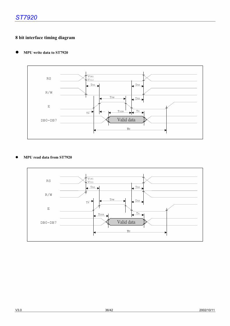
8 bit interface timing diagram
MPU write data to ST7920
MPU read data from ST7920
Valid data
RS
R/W
E
DB0-DB7
VIH1VIL1
TAS TAH
TAHTPWTR
TDDR TH
TCTC
Valid data
RS
R/W
E
DB0-DB7
VIH1VIL1
TAS TAH
TAHTPW
TH
TCTC
TDSWTR
ST7920
V3.0 37/42 2002/10/11
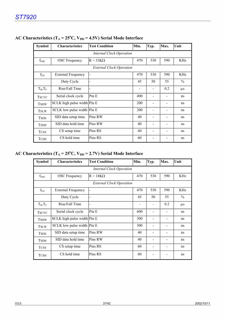
AC Characteristics (TA = 25oC, VDD = 4.5V) Serial Mode Interface
Symbol Characteristics Test Condition Min. Typ. Max. Unit
Internal Clock Operation
fOSC OSC Frequency R = 33KΩ 470 530 590 KHz
External Clock Operation
fEX External Frequency - 470 530 590 KHz
Duty Cycle - 45 50 55 %
TR,TF Rise/Fall Time - - - 0.2 µs
TSCYC Serial clock cycle Pin E 400 - - ns
TSHW SCLK high pulse width Pin E 200 - - ns
TSLW SCLK low pulse width Pin E 200 - - ns
TSDS SID data setup time Pins RW 40 - - ns
TSDH SID data hold time Pins RW 40 - - ns
TCSS CS setup time Pins RS 60 - - ns
TCSH CS hold time Pins RS 60 - - ns
AC Characteristics (TA = 25oC, VDD = 2.7V) Serial Mode Interface
Symbol Characteristics Test Condition Min. Typ. Max. Unit
Internal Clock Operation
fOSC OSC Frequency R = 18KΩ 470 530 590 KHz
External Clock Operation
fEX External Frequency - 470 530 590 KHz
Duty Cycle - 45 50 55 %
TR,TF Rise/Fall Time - - - 0.2 µs
TSCYC Serial clock cycle Pin E 600 - - ns
TSHW SCLK high pulse width Pin E 300 - - ns
TSLW SCLK low pulse width Pin E 300 - - ns
TSDS SID data setup time Pins RW 40 - - ns
TSDH SID data hold time Pins RW 40 - - ns
TCSS CS setup time Pins RS 60 - - ns
TCSH CS hold time Pins RS 60 - - ns
ST7920
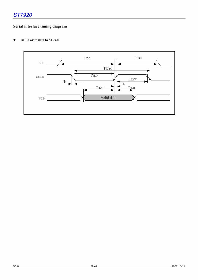
V3.0 38/42 2002/10/11
Serial interface timing diagram
MPU write data to ST7920
Valid data
CS
SID
SCLK
TCSS TCSH
TSCYC
TSLW
TSHW
TSDS
Tr
TSDH
Tf
ST7920
V3.0 39/42 2002/10/11
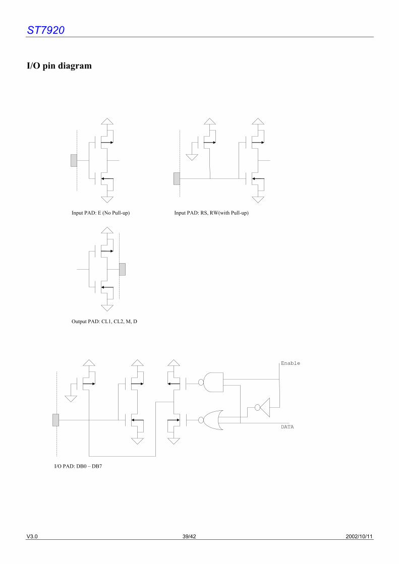
I/O pin diagram
Input PAD: E (No Pull-up) Input PAD: RS, RW(with Pull-up)
Output PAD: CL1, CL2, M, D
I/O PAD: DB0 – DB7
DATA
Enable
ST7920
V3.0 40/42 2002/10/11
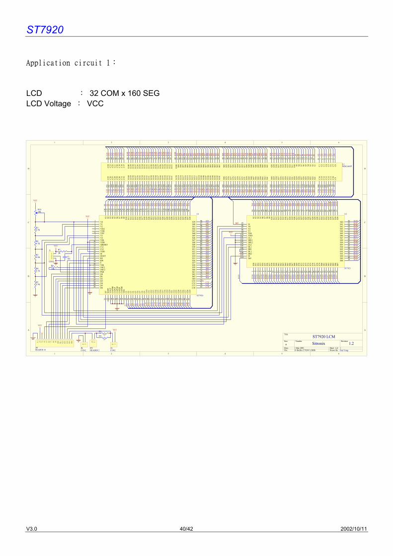
Application circuit 1:
LCD : 32 COM x 160 SEG LCD Voltage : VCC
1 2 3 4 5 6
A
B
C
D
654321
D
C
B
A
Title
Number RevisionSize
B
Date: 1-Mar-2001 Sheet of File: D:\Buffer-2\7920V1.DDB Drawn By:
V01
V12
V23
VXA4
VXB5
VXC6
V37
V48
VSS9
VDD10
XRESET11
CL112
CL213
VDD14
M15
DOUT16
RS17
RW18
E19
VSS20
OSC121
OSC222
PSB23
D024
D125
D226
D327
D428
D529
D630
D7
31
XO
FF32
VO
UT
33
CA
P3M
34
CA
P1P
35
CA
P1M
36
CA
P2P
37
CA
P2M
38
VD
239
C1
40
C2
41
C3
42
C4
43
C5
44
C6
45
C7
46
C8
47
C9
48
C10
49
C11
50
C12
51
C13
52
C14
53
C15
54
C16
55
C17
56
C18
57
C19
58
C20
59
C21
60
C22
61
C23
62
C24
63
C25
64
C26
65
C27
66
C28
67
C29
68
C30 69C31 70C32 71C33 72S64 73S63 74S62 75S61 76S60 77S59 78S58 79S57 80S56 81S55 82S54 83S53 84S52 85S51 86S50 87S49 88S48 89S47 90S46 91S45 92S44 93S43 94S42 95S41 96S40 97S39 98
S38
99S3
710
0S3
610
1S3
510
2S3
410
3S3
310
4S3
210
5S3
110
6S3
010
7S2
910
8S2
810
9S2
711
0S2
611
1S2
511
2S2
411
3S2
311
4S2
211
5S2
111
6S2
011
7S1
911
8S1
811
9S1
712
0S1
612
1S1
512
2S1
412
3S1
312
4S1
212
5S1
112
6S1
012
7S9
128
S812
9S7
130
S613
1S5
132
S413
3S3
134
S213
5S1
136
U1
ST7920
S50
1
S51
2
S52
3
S53
4
S54
5
S55
6
S56
7
S57
8
S58
9
S59
10
S60
11
S61
12
S62
13
S63
14
S64
15
S65
16
S66
17
S67
18
S68
19
S69
20
S70
21
S71
22
S72
23
S73
24
S74
25
S75
26
S76
27
S77
28
S78
29
S79
30
S80
31
S81
32
S82
33
S83
34
S84
35
S85
36
S86
37
S87
38
S88 39S89 40S90 41S91 42S92 43S93 44S94 45S95 46S96 47S48 48S47 49S46 50S45 51S44 52S43 53S42 54S41 55S40 56
S39
57S3
858
S37
59S3
660
S35
61S3
462
S33
63S3
264
S31
65S3
066
S29
67S2
868
S27
69S2
670
S25
71S2
472
S23
73S2
274
S21
75S2
076
S19
77S1
878
S17
79S1
680
S15
81S1
482
S13
83S1
284
S11
85S1
086
S987
S888
S789
S690
S591
S492
S393
S294
S195
V096
V297
V398
VSS99
VDD100
CL1101
SHL1102
SHL2103
CL2104
DL1105
DR1106
DL2107
DR2108
M109
S49110
U2
ST7921
C8
1C
72
C6
3C
54
C4
5C
36
C2
7C
18
S19
S210
S311
S412
S513
S614
S715
S816
S917
S10
18S1
119
S12
20S1
321
S14
22S1
523
S16
24S1
725
S18
26S1
927
S20
28
S41
29S4
230
S43
31S4
432
S45
33S4
634
S47
35S4
836
S49
37S5
038
S51
39S5
240
S53
41S5
442
S55
43S5
644
S57
45S5
846
S59
47S6
048
S81
49S8
250
S83
51S8
452
S85
53S8
654
S87
55S8
856
S89
57S9
058
S91
59S9
260
S93
61S9
462
S95
63S9
664
S97
65S9
866
S99
67S1
0068
S121
69S1
2270
S123
71S1
2472
S125
73S1
2674
S127
75S1
2876
S129
77S1
3078
S131
79S1
3280
S133
81S1
3482
S135
83S1
3684
S137
85S1
3886
S139
87S1
4088
C17
89C
1890
C19
91C
2092
C21
93C
2294
C23
95C
2496
C9
97C
1098
C11
99C
1210
0C
1310
1C
1410
2C
1510
3C
1610
4
S21
105
S22
106
S23
107
S24
108
S25
109
S26
110
S27
111
S28
112
S29
113
S30
114
S31
115
S32
116
S33
117
S34
118
S35
119
S36
120
S37
121
S38
122
S39
123
S40
124
S61
125
S62
126
S63
127
S64
128
S65
129
S66
130
S67
131
S68
132
S69
133
S70
134
S71
135
S72
136
S73
137
S74
138
S75
139
S76
140
S77
141
S78
142
S79
143
S80
144
S101
145
S102
146
S103
147
S104
148
S105
149
S106
150
S107
151
S108
152
S109
153
S110
154
S111
155
S112
156
S113
157
S114
158
S115
159
S116
160
S117
161
S118
162
S119
163
S120
164
S141
165
S142
166
S143
167
S144
168
S145
169
S146
170
S147
171
S148
172
S149
173
S150
174
S151
175
S152
176
S153
177
S154
178
S155
179
S156
180
S157
181
S158
182
S159
183
S160
184
C32
185
C31
186
C30
187
C29
188
C28
189
C27
190
C26
191
C25
192
L1WDG1603P
C1104
1 2 3 4 5 6 7 8 9 10 11 12 13 14 15 16
JP1HEADER 16
12
JACON2
12
JKCON2
123
J1
CON3
R14.7K
R24.7K
R32.2K
R44.7K
R54.7K
R6
33K
R7
2K
R9
33R8
33
VCC
VCC
VCC
VCC
12
JP2HEADER 2
VCC
VCC
C1
C2
C3
C4
C5
C6
C7
C8
C9
C10
C11
C12
C13
C14
C15
C16
C17
C18
C19
C20
C21
C22
C23
C24
C25
C26
C27
C28
C29
C30C31C32
S39S40S41S42S43S44S45S46S47S48S49S50S51S52S53S54S55S56S57S58S59S60S61S62S63S64
S1 S2 S3 S4 S5 S6 S7 S8 S9 S10
S11
S12
S13
S14
S15
S16
S17
S18
S19
S20
S21
S22
S23
S24
S25
S26
S27
S28
S29
S30
S31
S32
S33
S34
S35
S36
S37
S38
S65
S66
S67
S68
S69
S70
S71
S72
S73
S74
S75
S76
S77
S78
S79
S80
S81
S82
S83
S84
S85
S86
S87
S88
S89
S90
S91
S92
S93
S94
S95
S96
S97
S98
S99
S100
S101
S102
S103
S104S105S106S107S108S109S110S111S112
S113
S114
S115
S116
S117
S118
S119
S120
S121
S122
S123
S124
S125
S126
S127
S128
S129
S130
S131
S132
S133
S134
S135
S136
S137
S138
S139
S140
S141
S142
S143
S144
S145
S146
S147
S148
S149
S150
S151
S152S153S154S155S156S157S158S159S160
C25
C26
C27
C28
C29
C30
C31
C32
C1
C2
C3
C4
C5
C6
C7
C8
C9
C10
C11
C12
C13
C14
C15
C16
C17
C18
C19
C20
C21
C22
C23
C24
S1S2S3S4S5S6S7S8S9S10
S11
S12
S13
S14
S15
S16
S17
S18
S19
S20
S21
S22
S23
S24
S25
S26
S27
S28
S29
S30
S31
S32
S33
S34
S35
S36
S37
S38
S39
S40
S41
S42
S43
S44
S45
S46
S47
S48
S49
S50
S51
S52
S53
S54
S55
S56
S57
S58
S59
S60
S61
S62
S63
S64
S65
S66
S67
S68
S69
S70
S71
S72
S73
S74
S75
S76
S77
S78
S79
S80
S81
S82
S83
S84
S85
S86
S87
S88
S89
S90
S91
S92
S93
S94
S95
S96
S97
S98
S99
S100
S101
S102
S103
S104
S105
S106
S107
S108
S109
S110
S111
S112
S113
S114
S115
S116
S117
S118
S119
S120
S121
S122
S123
S124
S125
S126
S127
S128
S129
S130
S131
S132
S133
S134
S135
S136
S137
S138
S139
S140
S141
S142
S143
S144
S145
S146
S147
S148
S149
S150
S151
S152
S153
S154
S155
S156
S157
S158
S159
S160
Paul Yung1 1
1.2Sitronix
ST7920 LCM
R1010K
ST7920
V3.0 41/42 2002/10/11
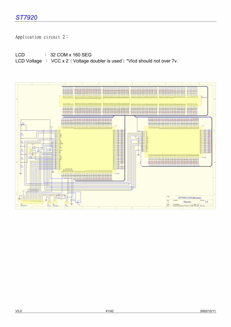
Application circuit 2:
LCD : 32 COM x 160 SEG LCD Voltage : VCC x 2(Voltage doubler is used)*Vlcd should not over 7v.
1 2 3 4 5 6
A
B
C
D
654321
D
C
B
A
Title
Number RevisionSize
B
Date: 17-Aug-2001 Sheet of File: D:\adom\Documents\sch\7920_B~13.DDB Drawn By:
V01
V12
V23
VXA4
VXB5
VXC6
V37
V48
VSS9
VDD10
XRESET11
CL112
CL213
VDD14
M15
DOUT16
RS17
RW18
E19
VSS20
OSC121
OSC222
PSB23
D024
D125
D226
D327
D428
D529
D630
D7
31
XO
FF32
VO
UT
33
CA
P3M
34
CA
P1P
35
CA
P1M
36
CA
P2P
37
CA
P2M
38
VD
239
C1
40
C2
41
C3
42
C4
43
C5
44
C6
45
C7
46
C8
47
C9
48
C10
49
C11
50
C12
51
C13
52
C14
53
C15
54
C16
55
C17
56
C18
57
C19
58
C20
59
C21
60
C22
61
C23
62
C24
63
C25
64
C26
65
C27
66
C28
67
C29
68
C30 69C31 70C32 71C33 72S64 73S63 74S62 75S61 76S60 77S59 78S58 79S57 80S56 81S55 82S54 83S53 84S52 85S51 86S50 87S49 88S48 89S47 90S46 91S45 92S44 93S43 94S42 95S41 96S40 97S39 98
S38
99S3
710
0S3
610
1S3
510
2S3
410
3S3
310
4S3
210
5S3
110
6S3
010
7S2
910
8S2
810
9S2
711
0S2
611
1S2
511
2S2
411
3S2
311
4S2
211
5S2
111
6S2
011
7S1
911
8S1
811
9S1
712
0S1
612
1S1
512
2S1
412
3S1
312
4S1
212
5S1
112
6S1
012
7S9
128
S812
9S7
130
S613
1S5
132
S413
3S3
134
S213
5S1
136
U1
ST7920
S50
1
S51
2
S52
3
S53
4
S54
5
S55
6
S56
7
S57
8
S58
9
S59
10
S60
11
S61
12
S62
13
S63
14
S64
15
S65
16
S66
17
S67
18
S68
19
S69
20
S70
21
S71
22
S72
23
S73
24
S74
25
S75
26
S76
27
S77
28
S78
29
S79
30
S80
31
S81
32
S82
33
S83
34
S84
35
S85
36
S86
37
S87
38
S88 39S89 40S90 41S91 42S92 43S93 44S94 45S95 46S96 47S48 48S47 49S46 50S45 51S44 52S43 53S42 54S41 55S40 56
S39
57S3
858
S37
59S3
660
S35
61S3
462
S33
63S3
264
S31
65S3
066
S29
67S2
868
S27
69S2
670
S25
71S2
472
S23
73S2
274
S21
75S2
076
S19
77S1
878
S17
79S1
680
S15
81S1
482
S13
83S1
284
S11
85S1
086
S987
S888
S789
S690
S591
S492
S393
S294
S195
V096
V297
V398
VSS99
VDD100
CL1101
SHL1102
SHL2103
CL2104
DL1105
DR1106
DL2107
DR2108
M109
S49110
U2
ST7921
C8
1C
72
C6
3C
54
C4
5C
36
C2
7C
18
S19
S210
S311
S412
S513
S614
S715
S816
S917
S10
18S1
119
S12
20S1
321
S14
22S1
523
S16
24S1
725
S18
26S1
927
S20
28
S41
29S4
230
S43
31S4
432
S45
33S4
634
S47
35S4
836
S49
37S5
038
S51
39S5
240
S53
41S5
442
S55
43S5
644
S57
45S5
846
S59
47S6
048
S81
49S8
250
S83
51S8
452
S85
53S8
654
S87
55S8
856
S89
57S9
058
S91
59S9
260
S93
61S9
462
S95
63S9
664
S97
65S9
866
S99
67S1
0068
S121
69S1
2270
S123
71S1
2472
S125
73S1
2674
S127
75S1
2876
S129
77S1
3078
S131
79S1
3280
S133
81S1
3482
S135
83S1
3684
S137
85S1
3886
S139
87S1
4088
C17
89C
1890
C19
91C
2092
C21
93C
2294
C23
95C
2496
C9
97C
1098
C11
99C
1210
0C
1310
1C
1410
2C
1510
3C
1610
4
S21
105
S22
106
S23
107
S24
108
S25
109
S26
110
S27
111
S28
112
S29
113
S30
114
S31
115
S32
116
S33
117
S34
118
S35
119
S36
120
S37
121
S38
122
S39
123
S40
124
S61
125
S62
126
S63
127
S64
128
S65
129
S66
130
S67
131
S68
132
S69
133
S70
134
S71
135
S72
136
S73
137
S74
138
S75
139
S76
140
S77
141
S78
142
S79
143
S80
144
S101
145
S102
146
S103
147
S104
148
S105
149
S106
150
S107
151
S108
152
S109
153
S110
154
S111
155
S112
156
S113
157
S114
158
S115
159
S116
160
S117
161
S118
162
S119
163
S120
164
S141
165
S142
166
S143
167
S144
168
S145
169
S146
170
S147
171
S148
172
S149
173
S150
174
S151
175
S152
176
S153
177
S154
178
S155
179
S156
180
S157
181
S158
182
S159
183
S160
184
C32
185
C31
186
C30
187
C29
188
C28
189
C27
190
C26
191
C25
192
L1WDG1603P
+ C34.7u
+
C2
4.7u
C1104
1 2 3 4 5 6 7 8 9 10 11 12 13 14 15 16
JP1HEADER 16
12
JACON2
12
JKCON2
123
J1
CON3
R14.7K
R24.7K
R32.2K
R44.7K
R54.7K
R6
33K
R7
2K
R9
33R8
33
VCC
VCC
VCC
12
JP2HEADER 2
VCC
VCC
C1
C2
C3
C4
C5
C6
C7
C8
C9
C10
C11
C12
C13
C14
C15
C16
C17
C18
C19
C20
C21
C22
C23
C24
C25
C26
C27
C28
C29
C30C31C32
S39S40S41S42S43S44S45S46S47S48S49S50S51S52S53S54S55S56S57S58S59S60S61S62S63S64
S1 S2 S3 S4 S5 S6 S7 S8 S9 S10
S11
S12
S13
S14
S15
S16
S17
S18
S19
S20
S21
S22
S23
S24
S25
S26
S27
S28
S29
S30
S31
S32
S33
S34
S35
S36
S37
S38
S65
S66
S67
S68
S69
S70
S71
S72
S73
S74
S75
S76
S77
S78
S79
S80
S81
S82
S83
S84
S85
S86
S87
S88
S89
S90
S91
S92
S93
S94
S95
S96
S97
S98
S99
S100
S101
S102
S103
S104S105S106S107S108S109S110S111S112
S113
S114
S115
S116
S117
S118
S119
S120
S121
S122
S123
S124
S125
S126
S127
S128
S129
S130
S131
S132
S133
S134
S135
S136
S137
S138
S139
S140
S141
S142
S143
S144
S145
S146
S147
S148
S149
S150
S151
S152S153S154S155S156S157S158S159S160
C25
C26
C27
C28
C29
C30
C31
C32
C1
C2
C3
C4
C5
C6
C7
C8
C9
C10
C11
C12
C13
C14
C15
C16
C17
C18
C19
C20
C21
C22
C23
C24
S1S2S3S4S5S6S7S8S9S10
S11
S12
S13
S14
S15
S16
S17
S18
S19
S20
S21
S22
S23
S24
S25
S26
S27
S28
S29
S30
S31
S32
S33
S34
S35
S36
S37
S38
S39
S40
S41
S42
S43
S44
S45
S46
S47
S48
S49
S50
S51
S52
S53
S54
S55
S56
S57
S58
S59
S60
S61
S62
S63
S64
S65
S66
S67
S68
S69
S70
S71
S72
S73
S74
S75
S76
S77
S78
S79
S80
S81
S82
S83
S84
S85
S86
S87
S88
S89
S90
S91
S92
S93
S94
S95
S96
S97
S98
S99
S100
S101
S102
S103
S104
S105
S106
S107
S108
S109
S110
S111
S112
S113
S114
S115
S116
S117
S118
S119
S120
S121
S122
S123
S124
S125
S126
S127
S128
S129
S130
S131
S132
S133
S134
S135
S136
S137
S138
S139
S140
S141
S142
S143
S144
S145
S146
S147
S148
S149
S150
S151
S152
S153
S154
S155
S156
S157
S158
S159
S160
Paul Yang1 1
1.4Sitronix
ST7920 LCM (Booster)
R1010K
ST7920
V3.0 42/42 2002/10/11
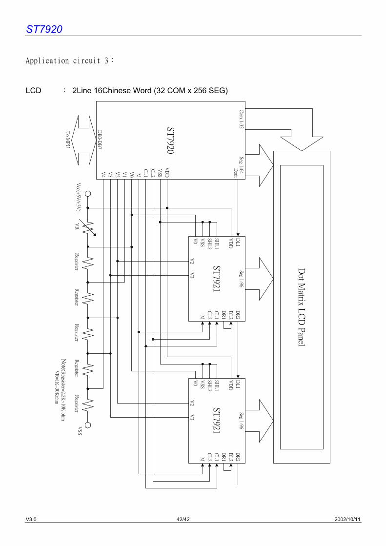
ST
7920
Dot M
atrix LC
D P
anel
VS
SV
cc(+5V
/+3V
)
DB
0-DB
7
To M
PU
V4
V3
V2
V1
V0 M
CL
1
CL
2
VS
S
VD
D
Seg 1-64
Com
1-32
Note:R
egsister=2.2K
~10K
ohm
VR
=1K
~30K
ohm
ST
7921
V2
V3
V0
VS
S
SH
L2
SH
L1
VD
D
DL
1
M
CL
2
CL
1
DR
1
DL
2
DR
2S
eg 1-96
ST
7921
V2
V3
V0
VS
S
SH
L2
SH
L1
VD
D
DL
1
M
CL
2
CL
1
DR
1
DL
2
DR
2S
eg 1-96
Regsister
Regsister
Regsister
Regsister
Regsister
VR
Dout
Application circuit 3:
LCD : 2Line 16Chinese Word (32 COM x 256 SEG)


![A High-Speed 64-Bit Binary Comparator€¦ · A high-speed 64-bit binary comparator 39 | Page III. EXISTING 64-BIT BINARY COMPARATOR DESIGN 64-bit comparator in reference [8], [9],](https://img.pdfslide.us/doc/110x75/5eac1a458d19873e777698b4/a-high-speed-64-bit-binary-comparator-a-high-speed-64-bit-binary-comparator-39-.jpg)