Embed Size (px)
Citation preview

165
SIMULATION OF SEMICONDUCTOR DEVICES AND PROCESSES Vol. 3 Edited by G, Baccarani, M. Rudan - Bologna (Italy) September 26-28, 1988 - Tccnoprinl
SITAR - An Efficient 3 D-Simulator for Optimization of Non-planar Trench Structures
W. Bergner and R. Kircher, SIEMENS AG, Corporate Research and Development, Otto-Hahn-Ring 6, 8000 MUnchen, West-Germany
SUMMARY
A 3-dimensional device simulator is presented which allows the investigation of the electrical behaviour of non-planar trench-type device structures. It has been used to analyze leakage due to punch through between neighbouring trench capacitors, depending on geometry and doping profiles. By its completely vectorized solution algorithm it proved to be a very efficient tool to optimize the cell size of 4 Megabit DRAMs.
INTRODUCTION
With increasing packing density the geometrical size of the single device structure becomes smaller and smaller. For the 4 Megabit DRAM the minimum feature size is 0.5 ium. However, some structures, especially storage capacitors, need a minimum area to maintain safe circuit operation. In VLSI dynamic memories the storage capacitor is extended into the bulk material as a so-called trench capacitor, leading to a 3-dimensional behaviour with parasitic effects, e. g. leakage current due to punch through. To optimize the geometry parameters of such a cell structure for use in modern 4 Megabit or 16 Megabit DRAMs, one has to include all effects arising from the 3-dimensional geometry, especially for nonuniform doping distributions. The 3-dimensional device simulator SITAR (Siemens Tr e n c n AnalyzeR.) has been developed to investigate the electrical behaviour of non-planar trench-type cell structures, depending on geometry, doping profiles and applied voltages. In this paper SITAR has been used to optimize the leakage behaviour of 4 Megabit DRAMs due to punch through between neighbouring trench capacitors.
166
THE SIMULATOR
The device simulator SITAR solves the phenomenological semiconductor equations
(1) v-ev¥ = -q (p - n + N+ - N~)
(2)
with
(3)
*-J^n = G - R
v-Tp = G - R
kT, U n(nv¥ - — v n
Dp = -|ip(pv*-+ |ivp;
in steady state and in 3 difference method, where ^ p and n the carrier densities, and j current densities.
dimensions by using the finite is the electrostatic potential,
and j the corresponding
The finite difference mesh has to be defined by the user and is kept fixed during the simulation. By introducing a box integration algorithm for the current continuity equations it becomes possible to treat general non-planar interfaces between the silicon area and different dielectric materials. Special routines for the discretization guarantee an accurate resolution of non-planar interfaces.
The number as well as the combination of the equations to be solved in a Gummel's cycle can be chosen. The stopping criterion for the corrections in the linear and in the nonlinear equations can be specified by the user. To find an efficient solution method for the inversion of the very large sparse matrix poses a rather complicated problem. For the simulations presented in this paper we have chosen a SOR-technique. The advantage of this algorithm is the high vectorization rate, which is almost 100 X in the presently implemented solver. In contrast to the vectorization is the rather slow convergence, especially for non-symmetric matrices, e. g. the discretized continuity equations.
Under various boundary conditions implemented in SITAR are Dirichlet conditions for ohmic and gate contacts, and Neumann conditions for artificial boundaries, e. g. device boundaries. Thin gate oxides can be treated analytically by a formula for an 1-dimensional MOS capacitor.
167
The 3-dimensional doping distribution can be defined either by a user-written subroutine or taken from ID or 2D process simulations together with a suitable extension into the other dimensions. For trench-type structures a universal parameterization for the geometry and the doping profiles has been developed.
The physical models implemented in SITAE include scattering on ionized impurities, lattice and carriers [1], In the mobility of electrons and holes, saturation of the field dependent velocity [2] is taken into account. High doping effects are included via band gap narrowing [3]. The generation/recombination model contains the mechanism of Shockley, Read and Hall and the Auger-effect, Impact ionization is not included in the generation model, but the ionization integral can be estimated by a post-processing calculation to find the breakdown voltage at reverse biased pn-junctions.
To minimize the computational effort for the trench cell optimization an analytical solution of the 1-dimensional continuity equation has been derived. For the case of punch through currents an expression similar to the subthreshold current of a MOSFET is obtained [4],
(4) xp t = q^i^n^eff^effl exp(q*0/kT),
where L ff is the effective length and A ££ the effective cross section of the leakage channel at the saddle point rQ of the potential distribution between neighbouring trenches, n-and ,u are the intrinsic carrier density and the electron mobility, respectively [4]. The parameters ^ , Lefc and Aef£ can be determined by the 3-dimensional solution of Poisson's equation.
(5) * o = * ( £ o )
trench 2
(6} L e f f = J exp{q(¥0-¥)/kT} dx
trench 1
Aeff = J exp{q(¥-¥o)/kT} dydz
cross sect.
168
Selecting this analytical model, the terminal currents are estimated as a function of the applied voltages, and the computational effort for the calculation of the I-V characteristic by the full 3-dimensional equations can be reduced drastically. The current values calculated by the analytical model and the 3-dimensional continuity equations agree within one order of magnitude.
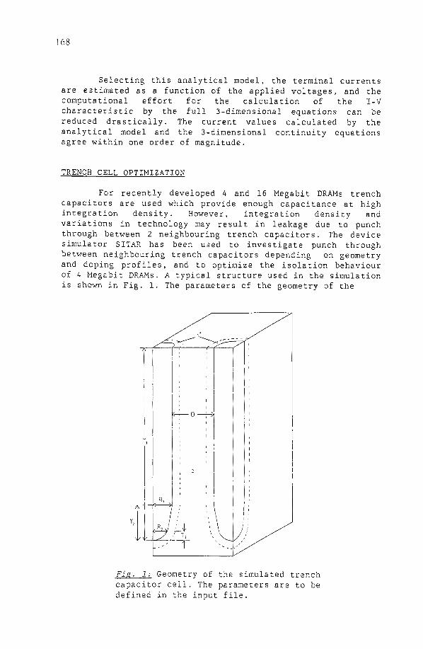
TRENCH CELL OPTIMIZATION
For recently developed 4 and 16 Megabit DRAMs trench capacitors are used which provide enough capacitance at high integration density. However, integration density and variations in technology may result in leakage due to punch through between 2 neighbouring trench capacitors. The device simulator SITAR has been used to investigate punch through between neighbouring trench capacitors depending on geometry and doping profiles, and to optimize the isolation behaviour of 4 Megabit DRAMs. A typical structure used in the simulation is shown in Fig. 1. The parameters of the geometry of the
Fin. 1: Geometry of the simulated trench capacitor cell. The parameters are to be defined in the input file.
169
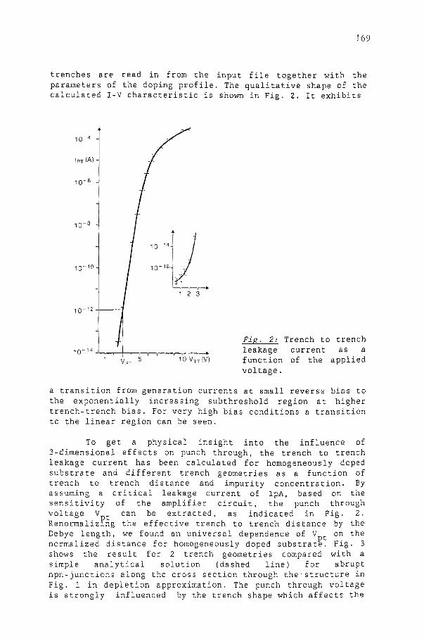
trenches are read in from the input file together with the parameters of the doping profile. The qualitative shape of the calculated I-V characteristic is shown in Fig. 2. It exhibits
1 0 V T T (V)
Fig. 2: Trench to trench leakage current as a function of the applied voltage.
a transition from generation currents at small reverse bias to the exponentially increasing subthreshold region at higher trench-trench bias. For very high bias conditions a transition to the linear region can be seen.
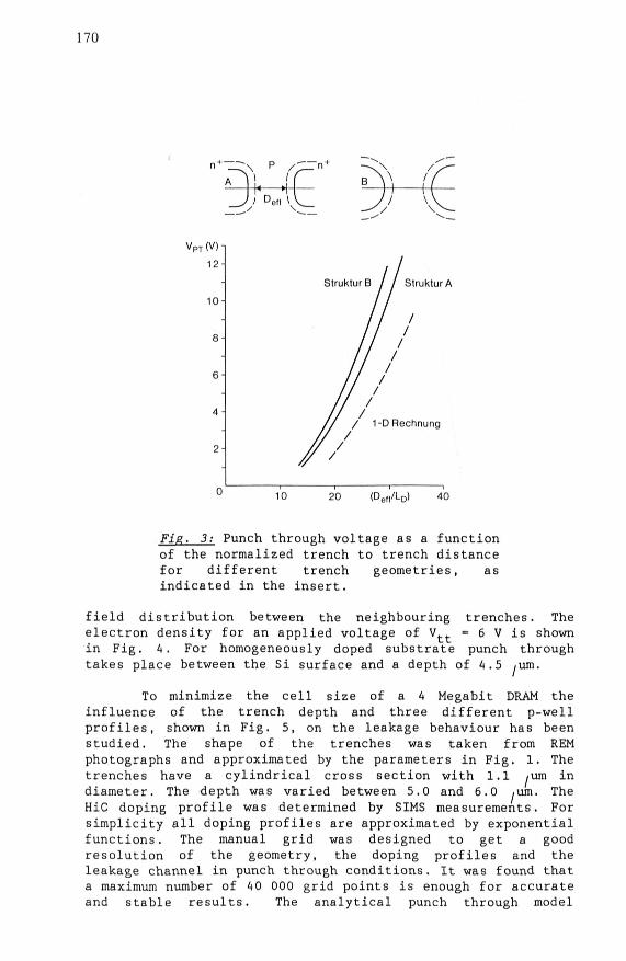
To get a physical insight into the influence of 3-dimensional effects on punch through, the trench to trench leakage current has been calculated for homogeneously doped substrate and different trench geometries as a function of trench to trench distance and impurity concentration. By assuming a critical leakage current of lpA, based on the sensitivity of the amplifier circuit, the punch through voltage V can be extracted, as indicated in Fig. 2. Renormalizmg the effective trench to trench distance by the Debye length, we found an universal dependence of V on the normalized distance for homogeneously doped substrate. Fig. 3 shows the result for 2 trench geometries compared with a simple analytical solution (dashed line) for abrupt npn-junctions along the cross section through the•structure in Fig. 1 in depletion approximation. The punch through voltage is strongly influenced by the trench shape which affects the
170
VPT (V)
12-
10
StrukturB / / StrukturA
Rechnung
10 20 (DeH/LD) 40
Fig. 3: Punch through voltage as a function of the normalized trench to trench distance for different trench geometries, as indicated in the insert.
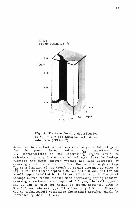
field distribution between the neighbouring trenches. The electron density for an applied voltage of Vfct • 6 V is shown in Fig. 4. For homogeneously doped substrate punch through takes place between the Si surface and a depth of 4.5 urn.
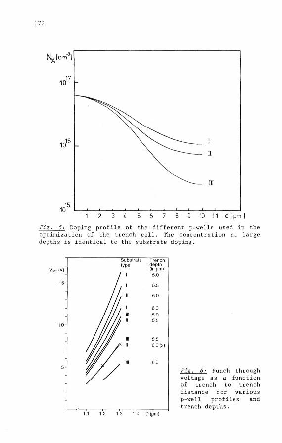
To minimize the cell size of a 4 Megabit DRAM the influence of the trench depth and three different p-well profiles, shown in Fig. 5, on the leakage behaviour has been studied. The shape of the trenches was taken from REM photographs and approximated by the parameters in Fig. 1. The trenches have a cylindrical cross section with 1.1 /tun in diameter. The depth was varied between 5.0 and 6.0 .um. The HiC doping profile was determined by SIMS measurements. For simplicity all doping profiles are approximated by exponential functions. The manual grid was designed to get a good resolution of the geometry, the doping profiles and the leakage channel in punch through conditions. It was found that a maximum number of 40 000 grid points is enough for accurate and stable results. The analytical punch through model
171
SITAR: Electron density (cm d) -3v
yCjjm]
2 . 8
6.B
8 . 0
xCpm] 2.0
Fig. 4: Electron density distribution at Vfct " 6 V for homogeneously doped substrate (2E16cm"3).
described in the last section was used to get a initial guess for the punch through voltage V t. Therefore the I-V characteristic in the interesting region could be calculated by only 3 - 4 selected voltages. From the leakage currents the punch through voltage has been extracted by assuming a critical current of lpA. The punch through voltage V t as a function of the trench to trench distance is shown in Fig. 6 for the trench depths 5.0, 5.5 and 6.0 /urn, and for the p-well types labelled by I, II and III in Fig. 5. The punch through curves become steeper with increasing doping density. Assuming a maximum trench depth of 5.5 ,um, the well types I and II can be used for trench to trench distances down to D - 1.2 /urn, whereas type III allows only 1.3 ium. However, due to technological variations the nominal distance should be increased by about 0.2 .urn.
\i:
NA[cm3
11 dt|im]
Fig. 5: Doping profile of the different p-wells used in the optimization of the trench cell. The concentration at large depths is identical to the substrate doping.
vPT (V)
15H
10H
Substrate type
Trench depth (in urn)
5.0
5.5
5.0
6.0 5.0 5.5
5.5 6.0 (x)
6.0
-M r-
Fig. 6: Punch through voltage as a function of trench to trench distance for various p-well profiles and trench depths.
1.1 1.2 1.3 1.4 D(um)
173
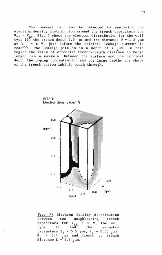
The leakage path can be detected by analyzing the electron density distribution around the trench capacitors for V t t < V fc. Fig. 7 shows the electron distribution for the well type II, the trench depth 5.5 ,um and the distance D - 1.2
r. at V t t - 6 V, just before the critical leakage current is reached. The leakage path is in a depth of 4 itim. In this region the ratio of effective trench-trench distance to Debye length has a maximum. Between the surface and the critical depth the doping concentration and for large depths the shape of the trench bottom inhibit punch through.
SITAR: Electron density ( cm 3 )
a.0
yCpn]
2 . 0
4 . 0
6.0
0 . 0
2 . 0
1.0
<[um] 2 . 0
£ 1.0
0.0 zCpn]
Fie.. 7: Electron density distribution between two neighbouring trench capacitors for Vtt - 6 V, the well type II and the geometry parameters T, R, - 0.4 , distance D - 1.2
urn 5.5 and trench
yum, n i • 0.55 to
/urn, trench
174
CONCLUSIONS
The 3-dimensional device simulator SITAR has been introduced which allows the analysis of trench type structures. It solves the classical semiconductor equations on a finite difference mesh by using Gummel's method and a very efficient solution algorithm for the linearized equations. The simulator has been used to investigate punch through between neighbouring trench capacitors depending on geometry and doping profiles, and to optimize the cell size for 4 Megabit DRAMs. The different punch through behaviour of trench capacitors in p-wells and those in homogeneously doped substrate results from a compression of the leakage channel by the 3-dimensional field distribution.
REFERENCES
[1] D. M. Caughey and R, F, Thomas,
"Carrier Mobility in Silicon Empirically Related to Doping and Field",
Proc. IEEE Vol. 54, (1967), 2192
[2] K. Yamaguchi,
"A Mobility Model tor Carriers in the MGS Inversion Layer",
IEEE Trans. Electron Devices, ED-30 (19835, 658
[3] J, W. Slocboom,
"The pr.-Product in Silicon",
Solid State Electronics Vol. 20, (1977), 279
['»] W. Bergner,
Master Thesis (in german), TU Munchen, 1988