Embed Size (px)
Citation preview
724 Volume 57, Number 6, 2003 APPLIED SPECTROSCOPY0003-7028 / 03 / 5706-0724$2.00 / 0q 2003 Society for Applied Spectroscopy
Single-Re� ection Attenuated TotalRe� ection of Organic Monolayers onSilicon
M. MILOSEVIC, S. L. BERETS,*and A. Y. FADEEVHarrick Scienti� c Corporation, Box 1288, 88 Broad-way, Ossining, New York 10562 (M.M., S.L.B.); andDepartment of Chemistry and Biochemistry, SetonHall University, 400 South Orange Avenue, SouthOrange, New Jersey 07079
Index Headings: Attenuated total re� ection; ATR; Internal re� ec-tion; Fourier transform infrared spectroscopy; FT-IR; Spectrosco-py; Monolayers; Thin � lms; Grazing angle spectroscopy; Siliconsubstrates.
INTRODUCTION
Attenuated total re� ection (ATR) spectroscopy, a well-known surface technique, is frequently used for exam-ining very thin � lms on substrates. However, when itcomes to examining thin � lms on silicon substrates, thehigh refractive index of the substrates seems to precludeATR analysis. This paper demonstrates that extraordinarysensitivity can be achieved by using ATR to analyzemonolayers on silicon.
THEORY
The theoretical foundations of the ATR technique wereprovided by Harrick and duPre1,2 early in the develop-ment of ATR as a spectroscopic technique. Harrick andduPre developed formulae for ATR analysis of very thin,weakly absorbing � lms deposited on a substrate, wherethe � lm thickness is much less than the wavelength.When the formulae are applied speci� cally to the case ofa thin � lm on a silicon substrate, using a Ge ATR crystaland an angle of incidence above the critical, the resultexhibits extraordinary sensitivity to thin � lms. This sen-sitivity enhancement was seized upon by Olsen and Shi-mura3,4 who calculated that, for the case of SiO2 � lm onSi wafer and the angle of incidence of 608, the enhance-ment was over 100 times per re� ection over what wouldhave been measured in transmission. In an attempt tofurther enhance the sensitivity, they used multiple re� ec-tion ATR in their experimental work. The results, whileimpressive, fall short of exhibiting the enhancement ofover 1500 that was predicted by the authors. Olsen andShimura did not discuss the degree of enhancement; theywere content with getting good experimental results.They probably did not achieve the predicted theoreticalenhancement due to imperfect contact between the sam-ple and the ATR crystal.
It is relatively straightforward to arrive at the expres-sion for the re� ectivity of a thin � lm sandwiched betweentwo media:5,6
Received 12 August 2002; accepted 31 January 2003.* Author to whom correspondence should be sent.
2 2 2p p 4p ikdÏn 2 n sin q2 1r 1 r e12 23pr 5 (1)2 2 2p p 4p ikdÏn 2 n sin q2 11 1 r r e12 23
where the index p indicates polarization of incident light,r and r are Fresnel amplitude coef� cients6 for the in-p p
12 23
terface between media (layers 1 and 3) and the � lm (layer2), k is the wavenumber (k 5 1/l), and q is the angle ofincidence of incident radiation. The refractive indices ofthe media could be complex to allow applicability of Eq.1 for the case of absorbing media. The expression in Eq.1 is the ratio of re� ected and incident electric-� eld am-plitudes. This expression describes the magnitude of there� ected electric � eld and the phase shift of the re� ected� eld with respect to the incident � eld. The square of theabsolute value of the amplitude coef� cient (see Eq. 1) isthe theoretical quantity to be compared to measured re-� ectance.
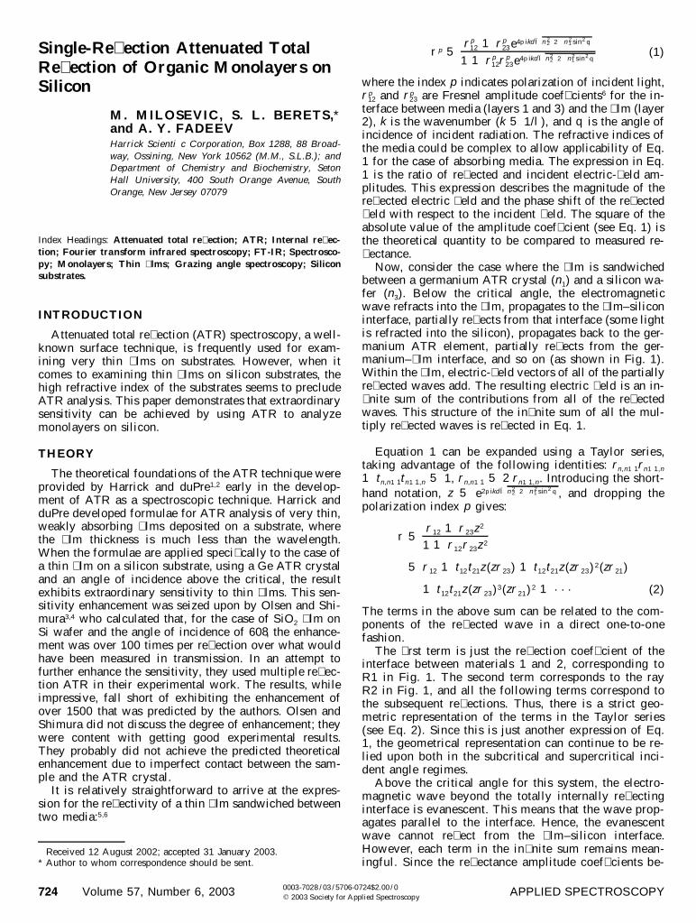
Now, consider the case where the � lm is sandwichedbetween a germanium ATR crystal (n1) and a silicon wa-fer (n3). Below the critical angle, the electromagneticwave refracts into the � lm, propagates to the � lm–siliconinterface, partially re� ects from that interface (some lightis refracted into the silicon), propagates back to the ger-manium ATR element, partially re� ects from the ger-manium–� lm interface, and so on (as shown in Fig. 1).Within the � lm, electric-� eld vectors of all of the partiallyre� ected waves add. The resulting electric � eld is an in-� nite sum of the contributions from all of the re� ectedwaves. This structure of the in� nite sum of all the mul-tiply re� ected waves is re� ected in Eq. 1.
Equation 1 can be expanded using a Taylor series,taking advantage of the following identities: rn,n1 1rn1 1,n
1 t n,n11t n11,n 5 1, r n,n11 5 2r n11,n. Introducing the short-hand notation, z 5 , and dropping the2 2 22p ikdÏn 2 n sin q2 1epolarization index p gives:
2r 1 r z12 23r 521 1 r r z12 23
25 r 1 t t z (zr ) 1 t t z (zr ) (zr )12 12 21 23 12 21 23 21
3 21 t t z (zr ) (zr ) 1 · · · (2)12 21 23 21
The terms in the above sum can be related to the com-ponents of the re� ected wave in a direct one-to-onefashion.
The � rst term is just the re� ection coef� cient of theinterface between materials 1 and 2, corresponding toR1 in Fig. 1. The second term corresponds to the rayR2 in Fig. 1, and all the following terms correspond tothe subsequent re� ections. Thus, there is a strict geo-metric representation of the terms in the Taylor series(see Eq. 2). Since this is just another expression of Eq.1, the geometrical representation can continue to be re-lied upon both in the subcritical and supercritical inci-dent angle regimes.
Above the critical angle for this system, the electro-magnetic wave beyond the totally internally re� ectinginterface is evanescent. This means that the wave prop-agates parallel to the interface. Hence, the evanescentwave cannot re� ect from the � lm–silicon interface.However, each term in the in� nite sum remains mean-ingful. Since the re� ectance amplitude coef� cients be-
APPLIED SPECTROSCOPY 725
FIG. 1. Multiple re� ections in the sample layer.
come of unit amplitude above the critical angle, thehigher terms in Eq. 2 become more signi� cant. For verythin � lms, the phase-shifts between the components arenegligible and the contributions to the electric-� eldcomponent perpendicular to the interface of all termsbecome constructive. This greatly enhances the electric-� eld strength within the � lm. Since the absorption isproportional to the square of the electric-� eld amplitude,an enhancement in the electric-� eld strength of ten timesresults in a hundredfold enhancement in absorption.
EXPERIMENTAL
Numerical simulations and experimental measure-ments were carried out to demonstrate this extraordinarysensitivity. Both used a germanium ATR crystal slightlyabove the critical angle to study an organic thin � lm ona silicon substrate.
For the numerical analysis, the experimental param-eters were selected as follows:
n 5 4.0 (germanium ATR crystal)1
n 5 1.5 1 0.5i (sample)2
n 5 3.45 (silicon substrate)3
21k 5 1000 cm (wavenumber of incident light,l 5 10 mm)
Êd 5 1 nm (10 A)
u 5 608
Note that a typical organic sample has the real part ofthe refractive index around 1.5; hence the above choice.The value of the imaginary part of the refractive index(i.e., absorption index, k) of the sample is chosen tocorrespond to the center of a fairly strong absorptionband. To get a sense of the strength of the absorptionindex chosen and thus be able to correlate the simulatedresults to actual samples, one can calculate the absor-bance that would be measured for this peak in a trans-mission measurement with a pathlength of d 5 10 mm.If the peak were located in the carbonyl region (k ø1700 cm2 1), the absorbance measured would be (ne-glecting the re� ectance losses):
A 5 0.434 3 4pkkd 5 4.6
This is a rather strong absorber, as stated above. The
results of the numerical simulation using these param-eters are presented graphically.
The supported organic monolayers were prepared bythe reaction of ClSi(CH3)2(CH2)3Si[OSi(CH3)3]3, furthersilane, with Si wafers (International Wafer Service,(100) orientation, P/B doped, resistivity from 20 to 40ohm-cm, thickness ;450–575 mm) according to the fol-lowing scheme:
The reaction procedure was similar to that published inearlier work.7 Brie� y, the synthesis included the follow-ing steps. Prior to the reaction with silane, Si waferswere cleaned using a freshly prepared solution madefrom seven parts of concentrated sulfuric acid, dissolvedsodium dichromate (;3–5 wt %), and three parts of 30%hydrogen peroxide. The Si wafers were submerged inthis cleaning solution overnight, rinsed with � ve to sev-en 50 mL aliquots of water, and placed in a clean ovenat 120 8C for 1–2 h. The dried Si plates were coveredwith anhydrous toluene (5–10 mL) containing ethyldi-isopropylamine (1023 M). Then 0.5 mL of silane wasadded by syringe and the reaction mixture was left atroom temperature for 3 days. The wafers were isolatedand rinsed sequentially with 2 3 10 mL of toluene, 3 310 mL of ethanol, 2 3 10 mL of an ethanol–water mix(1:1), 2 3 10 mL of water, 2 3 10 mL of ethanol, and2 3 10 mL of water. After rinsing, the wafers were driedin a clean oven at 120 8C for 10 min.
Ellipsometric characterization of bare Si wafers andSi-supported monolayers were made with an InomteckAutomatic Ellipsometer. The light source was a He–Nelaser with l 5 632.8 nm. The angle of incidence was708. Measurements were performed for 3–5 differentspots on the sample. The thickness of the layer was cal-culated from the ellipsometric parameters (D and C) us-ing the Inomteck software. The thickness of the siliconoxide overlayer on the Si substrate was calculated usingthe following settings: single-layer model, air: n0 5 1;silicon oxide layer: n2 5 1.462; silicon substrate: nS 53.858 1 0.018i. The thickness of silicon oxide for thebare Si wafers was 2.1 6 0.05 nm after the cleaning.For the Si supported monolayers, the calculations wereperformed for the transparent double-layer model (sili-con substrate/silicon oxide/alkylsilane layer/air) with thefollowing parameters: air: n0 5 1; alkylsilane layer: n1
5 1.45; silicon oxide layer: n2 5 1.462 (the thicknessof this oxide layer was � xed at 2.1 nm); silicon sub-strate: nS 5 3.858 1 0.018i. The thickness of the mono-layer was obtained as 0.9 6 0.1 nm.
The ATR measurements were carried out using Har-rick’s Seagull y ,8 variable angle re� ection accessoryused in conjunction with a Bruker Vector 22 spectrom-eter. A spectrum was collected with 32 scans, an 8 cm21
resolution, and a 658 incident angle. Note that the ex-perimental apparatus focuses the beam onto the sample
726 Volume 57, Number 6, 2003
FIG. 2. Absorbance of a thin � lm shown as a function of the refractiveindex of the substrate.
FIG. 4. The enhancement of absorbance due to the silicon substratevs. thickness.
FIG. 3. Absorbance vs. � lm thickness. FIG. 5. ATR spectrum of an organic monolayer on a silicon wafer.
and hence supplies a range of incident angles, as op-posed to the collimated beam assumed by the theoreticalmodel. To avoid contributions from rays below the crit-ical angle, the experimental incident angle was chosento be slightly higher than the angle used in the simula-tions.
The coated Si wafers were cut to � t into the ATRholder of the Seagull y . A special pressure applicatorwas used to optimize contact between the sample andthe ATR crystal.
RESULTS AND DISCUSSION
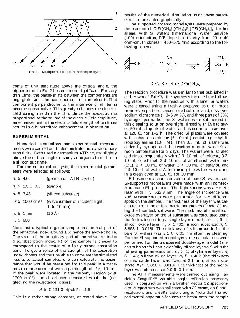
The results of the numerical analysis are shown inFigs. 2 through 4. Figure 2 shows the intriguing depen-dence of the measured absorbance of the thin � lm onthe refractive index of the substrate. The angle of inci-dence was kept constant at 608 and the absorption indexof the � lm at 0.5. The change in the refractive index ofthe substrate is between that of the thin � lm (1.5) andthe silicon wafer (3.45). The increase in sensitivity isremarkable. This clearly shows that the high refractive
index of the substrate is the crucial ingredient leadingto the increased sensitivity.
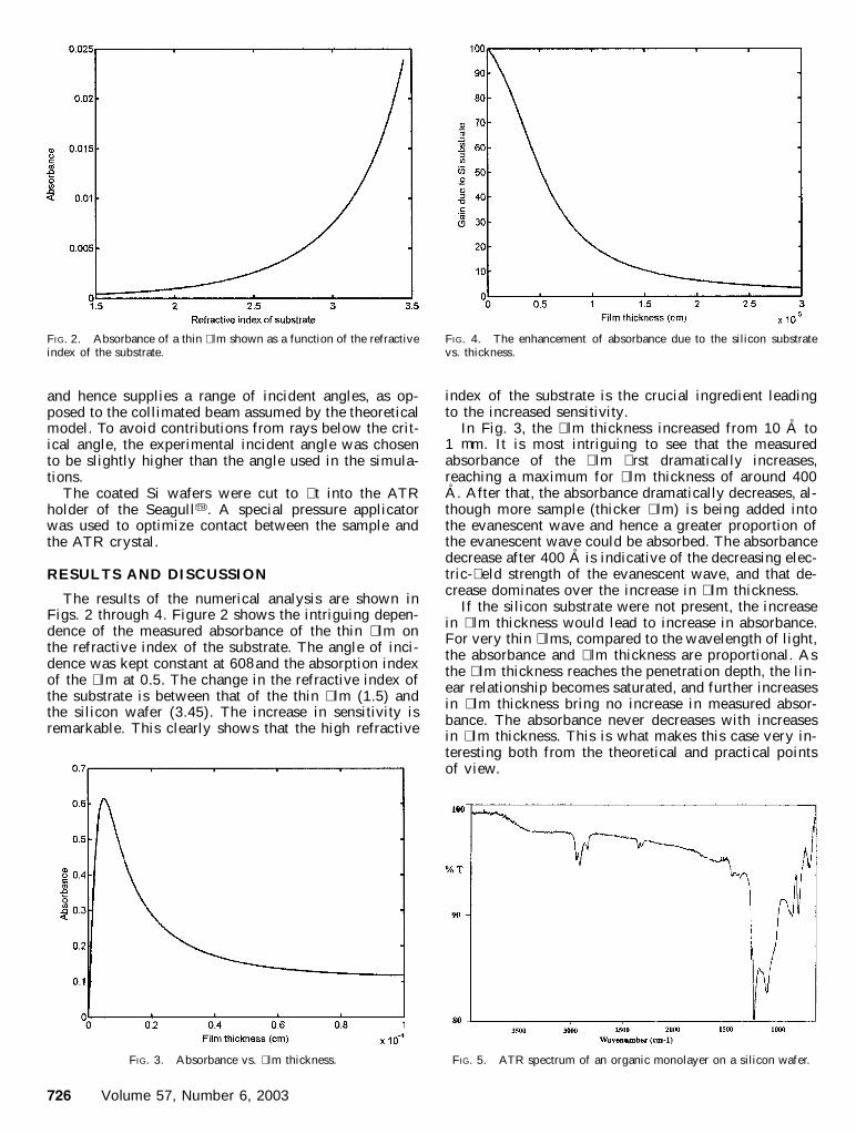
In Fig. 3, the � lm thickness increased from 10 AÊ to1 mm. It is most intriguing to see that the measuredabsorbance of the � lm � rst dramatically increases,reaching a maximum for � lm thickness of around 400AÊ . After that, the absorbance dramatically decreases, al-though more sample (thicker � lm) is being added intothe evanescent wave and hence a greater proportion ofthe evanescent wave could be absorbed. The absorbancedecrease after 400 AÊ is indicative of the decreasing elec-tric-� eld strength of the evanescent wave, and that de-crease dominates over the increase in � lm thickness.
If the silicon substrate were not present, the increasein � lm thickness would lead to increase in absorbance.For very thin � lms, compared to the wavelength of light,the absorbance and � lm thickness are proportional. Asthe � lm thickness reaches the penetration depth, the lin-ear relationship becomes saturated, and further increasesin � lm thickness bring no increase in measured absor-bance. The absorbance never decreases with increasesin � lm thickness. This is what makes this case very in-teresting both from the theoretical and practical pointsof view.
APPLIED SPECTROSCOPY 727
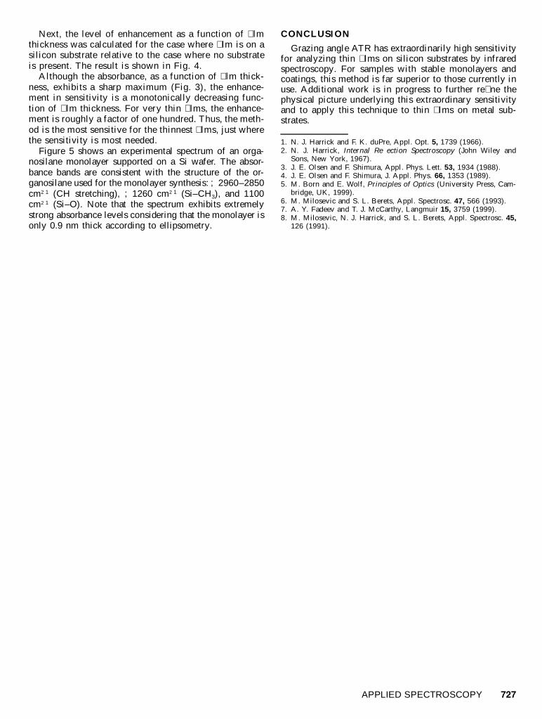
Next, the level of enhancement as a function of � lmthickness was calculated for the case where � lm is on asilicon substrate relative to the case where no substrateis present. The result is shown in Fig. 4.
Although the absorbance, as a function of � lm thick-ness, exhibits a sharp maximum (Fig. 3), the enhance-ment in sensitivity is a monotonically decreasing func-tion of � lm thickness. For very thin � lms, the enhance-ment is roughly a factor of one hundred. Thus, the meth-od is the most sensitive for the thinnest � lms, just wherethe sensitivity is most needed.
Figure 5 shows an experimental spectrum of an orga-nosilane monolayer supported on a Si wafer. The absor-bance bands are consistent with the structure of the or-ganosilane used for the monolayer synthesis: ;2960–2850cm21 (CH stretching), ;1260 cm21 (Si–CH3), and 1100cm21 (Si–O). Note that the spectrum exhibits extremelystrong absorbance levels considering that the monolayer isonly 0.9 nm thick according to ellipsometry.
CONCLUSION
Grazing angle ATR has extraordinarily high sensitivityfor analyzing thin � lms on silicon substrates by infraredspectroscopy. For samples with stable monolayers andcoatings, this method is far superior to those currently inuse. Additional work is in progress to further re� ne thephysical picture underlying this extraordinary sensitivityand to apply this technique to thin � lms on metal sub-strates.
1. N. J. Harrick and F. K. duPre, Appl. Opt. 5, 1739 (1966).2. N. J. Harrick, Internal Re� ection Spectroscopy (John Wiley and
Sons, New York, 1967).3. J. E. Olsen and F. Shimura, Appl. Phys. Lett. 53, 1934 (1988).4. J. E. Olsen and F. Shimura, J. Appl. Phys. 66, 1353 (1989).5. M. Born and E. Wolf, Principles of Optics (University Press, Cam-
bridge, UK, 1999).6. M. Milosevic and S. L. Berets, Appl. Spectrosc. 47, 566 (1993).7. A. Y. Fadeev and T. J. McCarthy, Langmuir 15, 3759 (1999).8. M. Milosevic, N. J. Harrick, and S. L. Berets, Appl. Spectrosc. 45,
126 (1991).