Embed Size (px)
Citation preview
M MCP6S21/2/6/8Single-Ended, Rail-to-Rail I/O, Low Gain PGA
Features• Multiplexed Inputs: 1, 2, 6 or 8 channels• 8 Gain Selections:
- +1, +2, +4, +5, +8, +10, +16 or +32 V/V• Serial Peripheral Interface (SPI™)• Rail-to-Rail Input and Output• Low Gain Error: ±1% (max)• Low Offset: ±275 µV (max)• High Bandwidth: 2 to 12 MHz (typ)• Low Noise: 10 nV/√Hz @ 10 kHz (typ)• Low Supply Current: 1.0 mA (typ)• Single Supply: 2.5V to 5.5V
Typical Applications• A/D Converter Driver• Multiplexed Analog Applications• Data Acquisition• Industrial Instrumentation• Test Equipment• Medical Instrumentation
Package Types
DescriptionThe Microchip Technology Inc. MCP6S21/2/6/8 areanalog Programmable Gain Amplifiers (PGA). Theycan be configured for gains from +1 V/V to +32 V/V andthe input multiplexer can select one of up to eight chan-nels through an SPI port. The serial interface can alsoput the PGA into shutdown to conserve power. ThesePGAs are optimized for high speed, low offset voltageand single-supply operation with rail-to-rail input andoutput capability. These specifications support singlesupply applications needing flexible performance ormultiple inputs.
The one channel MCP6S21 and the two channelMCP6S22 are available in 8-pin PDIP, SOIC andMSOP packages. The six channel MCP6S26 is avail-able in 14-pin PDIP, SOIC and TSSOP packages. Theeight channel MCP6S28 is available in 16-pin PDIPand SOIC packages. All parts are fully specified from-40°C to +85°C.
Block Diagram
VREF
CH0
VSS
SISCK
1234
8765
VDD
CS
VOUT
CH1CH0
CH2
CS
SI
1234
14131211
VREF
VSS
VOUT
567
1098
CH3
SCK
VDD
CH5CH4
CH0
VOUT
CH1
VSS
CS
1234
16151413 SI
SCK
567
121110
CH2
CH4
CH7
VDD
CH58 9
SO
CH6
CH3
SO
CH1CH0
VSS
SISCK
1234
8765
VDD
CS
VOUT
MCP6S21PDIP, SOIC, MSOP
MCP6S26PDIP, SOIC, TSSOP
MCP6S28PDIP, SOIC
MCP6S22PDIP, SOIC, MSOP
VREF
VOUT
VREF
VDD
CSSI
SOSCK
CH1CH0
CH3CH2
CH5CH4
CH7CH6
VSS
8RF
RG
MUX
SPI™Logic
POR
GainSwitches
+
- Resistor Ladder (R
LAD )
2003 Microchip Technology Inc. DS21117A-page 1
MCP6S21/2/6/8
1.0 ELECTRICALCHARACTERISTICS
Absolute Maximum Ratings †VDD - VSS .........................................................................7.0VAll inputs and outputs....................... VSS - 0.3V to VDD +0.3VDifference Input voltage ........................................ |VDD - VSS|Output Short Circuit Current...................................continuousCurrent at Input Pin .............................................................±2 mACurrent at Output and Supply Pins ................................ ±30 mAStorage temperature .....................................-65°C to +150°CJunction temperature ..................................................+150°CESD protection on all pins (HBM;MM).................. ≥ 2 kV; 200V† Notice: Stresses above those listed under "MaximumRatings" may cause permanent damage to the device. This isa stress rating only and functional operation of the device atthose or any other conditions above those indicated in theoperation listings of this specification is not implied. Exposureto maximum rating conditions for extended periods may affectdevice reliability.
PIN FUNCTION TABLE
Name Function
VOUT Analog OutputCH0-CH7 Analog Inputs
VSS Negative Power SupplyVDD Positive Power SupplySCK SPI Clock InputSI SPI Serial Data InputSO SPI Serial Data OutputCS SPI Chip Select
VREF External Reference Pin
DC CHARACTERISTICSElectrical Specifications: Unless otherwise indicated, TA = +25°C, VDD = +2.5V to +5.5V, VSS = GND, VREF = VSS, G = +1 V/V, Input = CH0 = (0.3V)/G, CH1 to CH7 = 0.3V, RL = 10 kΩ to VDD/2, SI and SCK are tied low and CS is tied high.
Parameters Sym Min Typ Max Units ConditionsAmplifier InputInput Offset Voltage VOS -275 — +275 µV G = +1, VDD = 4.0VInput Offset Voltage Drift ∆VOS/∆TA — ±4 — µV/°C TA = -40 to +85°CPower Supply Rejection Ratio PSRR 70 85 — dB G = +1 (Note 1)Input Bias Current IB — ±1 — pA CHx = VDD/2Input Bias Current overTemperature
IB — — 250 pA TA = -40 to +85°C,CHx = VDD/2
Input Impedance ZIN — 1013||15 — Ω||pFInput Voltage Range VIVR VSS−0.3 — VDD+0.3 VAmplifier GainNominal Gains G — 1 to 32 — V/V +1, +2, +4, +5, +8, +10, +16 or +32DC Gain Error G = +1 gE -0.1 — +0.1 % VOUT ≈ 0.3V to VDD − 0.3V
G ≥ +2 gE -1.0 — +1.0 % VOUT ≈ 0.3V to VDD − 0.3VDC Gain Drift G = +1 ∆G/∆TA — ±0.0002 — %/°C TA = -40 to +85°C
G ≥ +2 ∆G/∆TA — ±0.0004 — %/°C TA = -40 to +85°CInternal Resistance RLAD 3.4 4.9 6.4 kΩ (Note 1)Internal Resistance over Temperature
∆RLAD/∆TA — +0.028 — %/°C (Note 1)TA = -40 to +85°C
Amplifier OutputDC Output Non-linearity G = +1 VONL — ±0.003 — % of FSR VOUT = 0.3V to VDD − 0.3V, VDD = 5.0V
G ≥ +2 VONL — ±0.001 — % of FSR VOUT = 0.3V to VDD − 0.3V, VDD = 5.0VMaximum Output Voltage Swing VOH, VOL VSS+20 — VDD-100 mV G ≥ +2; 0.5V output overdrive
VSS+60 — VDD-60 G ≥ +2; 0.5V output overdrive,VREF = VDD/2
Short-Circuit Current IO(SC) — ±30 — mANote 1: RLAD (RF + RG in Figure 4-1) connects VREF, VOUT and the inverting input of the internal amplifier. The MCP6S22 has
VREF tied internally to VSS, so VSS is coupled to the internal amplifier and the PSRR spec describes PSRR+ only. We recommend the MCP6S22’s VSS pin be tied directly to ground to avoid noise problems.
2: IQ includes current in RLAD (typically 60 µA at VOUT = 0.3V). Both IQ and IQ_SHDN exclude digital switching currents.3: The output goes Hi-Z and the registers reset to their defaults; see Section 5.4, “Power-On Reset”.
DS21117A-page 2 2003 Microchip Technology Inc.
MCP6S21/2/6/8
Power SupplySupply Voltage VDD 2.5 — 5.5 VQuiescent Current IQ 0.5 1.0 1.35 mA IO = 0 (Note 2)Quiescent Current, Shutdown mode
IQ_SHDN — 0.5 1.0 µA IO = 0 (Note 2)
Power-On ResetPOR Trip Voltage VPOR 1.2 1.7 2.2 V (Note 3)POR Trip Voltage Drift ∆VPOR/∆T — -3.0 — mV/°C TA = -40°C to+85°C
DC CHARACTERISTICS (CONTINUED)Electrical Specifications: Unless otherwise indicated, TA = +25°C, VDD = +2.5V to +5.5V, VSS = GND, VREF = VSS, G = +1 V/V, Input = CH0 = (0.3V)/G, CH1 to CH7 = 0.3V, RL = 10 kΩ to VDD/2, SI and SCK are tied low and CS is tied high.
Parameters Sym Min Typ Max Units Conditions
Note 1: RLAD (RF + RG in Figure 4-1) connects VREF, VOUT and the inverting input of the internal amplifier. The MCP6S22 has VREF tied internally to VSS, so VSS is coupled to the internal amplifier and the PSRR spec describes PSRR+ only. We recommend the MCP6S22’s VSS pin be tied directly to ground to avoid noise problems.
2: IQ includes current in RLAD (typically 60 µA at VOUT = 0.3V). Both IQ and IQ_SHDN exclude digital switching currents.3: The output goes Hi-Z and the registers reset to their defaults; see Section 5.4, “Power-On Reset”.
AC CHARACTERISTICSElectrical Specifications: Unless otherwise indicated, TA = +25°C, VDD = +2.5V to +5.5V, VSS = GND, VREF = VSS, G = +1 V/V, Input = CH0 =(0.3V)/G, CH1 to CH7=0.3V, RL = 10 kΩ to VDD/2, CL = 60 pF, SI and SCK are tied low, and CS is tied high.
Parameters Sym Min Typ Max Units ConditionsFrequency Response-3 dB Bandwidth BW — 2 to 12 — MHz All gains; VOUT < 100 mVP-P (Note 1)Gain Peaking GPK — 0 — dB All gains; VOUT < 100 mVP-PTotal Harmonic Distortion plus Noise
f = 1 kHz, G = +1 V/V THD+N — 0.0015 — % VOUT = 1.5V ± 1.0VPK, VDD = 5.0V,BW = 22 kHz
f = 1 kHz, G = +4 V/V THD+N — 0.0058 — % VOUT = 1.5V ± 1.0VPK, VDD = 5.0V,BW = 22 kHz
f = 1 kHz, G = +16 V/V THD+N — 0.023 — % VOUT = 1.5V ± 1.0VPK, VDD = 5.0V,BW = 22 kHz
f = 20 kHz, G = +1 V/V THD+N — 0.0035 — % VOUT = 1.5V ± 1.0VPK, VDD = 5.0V,BW = 80 kHz
f = 20 kHz, G = +4 V/V THD+N — 0.0093 — % VOUT = 1.5V ± 1.0VPK, VDD = 5.0V,BW = 80 kHz
f = 20 kHz, G = +16 V/V THD+N — 0.036 — % VOUT = 1.5V ± 1.0VPK, VDD = 5.0V,BW = 80 kHz
Step ResponseSlew Rate SR — 4.0 — V/µs G = 1, 2
— 11 — V/µs G = 4, 5, 8, 10— 22 — V/µs G = 16, 32
NoiseInput Noise Voltage Eni — 3.2 — µVP-P f = 0.1 Hz to 10 kHz (Note 2)
— 26 — f = 0.1 Hz to 200 kHz (Note 2)Input Noise Voltage Density eni — 10 — nV/√Hz f = 10 kHz (Note 2)Input Noise Current Density ini — 4 — fA/√Hz f = 10 kHzNote 1: See Table 4-1 for a list of typical numbers.
2: Eni and eni include ladder resistance noise. See Figure 2-33 for eni vs. G data.
2003 Microchip Technology Inc. DS21117A-page 3

MCP6S21/2/6/8
DIGITAL CHARACTERISTICSElectrical Specifications: Unless otherwise indicated, TA = +25°C, VDD = +2.5V to +5.5V, VSS = GND, VREF = VSS, G = +1 V/V, Input = CH0 = (0.3V)/G, CH1 to CH7 = 0.3V, RL = 10 kΩ to VDD/2, CL = 60 pF, SI and SCK are tied low, and CS is tied high.Parameters Sym Min Typ Max Units Conditions
SPI Inputs (CS, SI, SCK)
Logic Threshold, Low VIL 0 — 0.3VDD VInput Leakage Current IIL -1.0 — +1.0 µALogic Threshold, High VIH 0.7VDD — VDD VAmplifier Output Leakage Current — -1.0 — +1.0 µA In Shutdown modeSPI Output (SO, for MCP6S26 and MCP6S28)Logic Threshold, Low VOL VSS — VSS+0.4 V IOL = 2.1 mA, VDD = 5VLogic Threshold, High VOH VDD-0.5 — VDD V IOH = -400 µASPI TimingPin Capacitance CPIN — 10 — pF All digital I/O pins
Input Rise/Fall Times (CS, SI, SCK) tRFI — — 2 µs Note 1
Output Rise/Fall Times (SO) tRFO — 5 — ns MCP6S26 and MCP6S28
CS high time tCSH 40 — — ns
SCK edge to CS fall setup time tCS0 10 — — ns SCK edge when CS is high
CS fall to first SCK edge setup time tCSSC 40 — — ns
SCK Frequency fSCK — — 10 MHz VDD = 5V (Note 2)SCK high time tHI 40 — — nsSCK low time tLO 40 — — ns
SCK last edge to CS rise setup time tSCCS 30 — — ns
CS rise to SCK edge setup time tCS1 100 — — ns SCK edge when CS is high
SI set-up time tSU 40 — — nsSI hold time tHD 10 — — nsSCK to SO valid propagation delay tDO — — 80 ns MCP6S26 and MCP6S28
CS rise to SO forced to zero tSOZ — — 80 ns MCP6S26 and MCP6S28
Channel and Gain Select TimingChannel Select Time tCH — 1.5 — µs CHx = 0.6V, CHy =0.3V, G = 1,
CHx to CHy selectCS = 0.7VDD to VOUT 90% point
Gain Select Time tG — 1 — µs CHx = 0.3V, G = 5 to G = 1 select,CS = 0.7VDD to VOUT 90% point
Shutdown Mode TimingOut of Shutdown mode (CS goes high) to Amplifier Output Turn-on Time
tON — 3.5 10 µs CS = 0.7VDD to VOUT 90% point
Into Shutdown mode (CS goes high) to Amplifier Output High-Z Turn-off Time
tOFF — 1.5 — µs CS = 0.7VDD to VOUT 90% point
POR TimingPower-On Reset power-up time tRPU — 30 — µs VDD = VPOR - 0.1V to VPOR + 0.1V,
50% VDD to 90% VOUT pointPower-On Reset power-down time tRPD — 10 — µs VDD = VPOR + 0.1V to VPOR - 0.1V,
50% VDD to 90% VOUT pointNote 1: Not tested in production. Set by design and characterization.
2: When using the device in the daisy chain configuration, maximum clock frequency is determined by a combination of propagation delay time (tDO ≤ 80 ns), data input setup time (tSU ≥ 40 ns), SCK high time (tHI ≥ 40 ns), and SCK rise and fall times of 5 ns. Maximum fSCK is, therefore, ≈ 5.8 MHz.
DS21117A-page 4 2003 Microchip Technology Inc.
MCP6S21/2/6/8
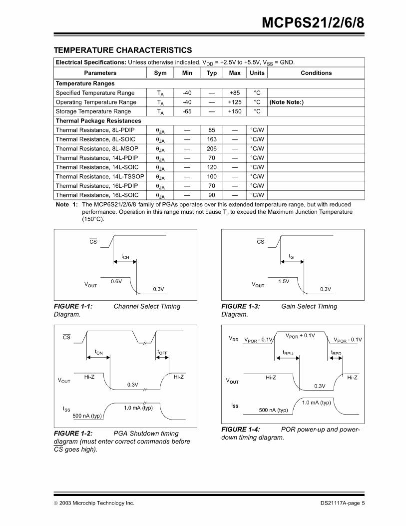
TEMPERATURE CHARACTERISTICSFIGURE 1-1: Channel Select Timing Diagram.
FIGURE 1-2: PGA Shutdown timing diagram (must enter correct commands before CS goes high).
FIGURE 1-3: Gain Select Timing Diagram.
FIGURE 1-4: POR power-up and power-down timing diagram.
Electrical Specifications: Unless otherwise indicated, VDD = +2.5V to +5.5V, VSS = GND.
Parameters Sym Min Typ Max Units Conditions
Temperature RangesSpecified Temperature Range TA -40 — +85 °COperating Temperature Range TA -40 — +125 °C (Note Note:)Storage Temperature Range TA -65 — +150 °CThermal Package ResistancesThermal Resistance, 8L-PDIP θJA — 85 — °C/WThermal Resistance, 8L-SOIC θJA — 163 — °C/WThermal Resistance, 8L-MSOP θJA — 206 — °C/WThermal Resistance, 14L-PDIP θJA — 70 — °C/WThermal Resistance, 14L-SOIC θJA — 120 — °C/WThermal Resistance, 14L-TSSOP θJA — 100 — °C/WThermal Resistance, 16L-PDIP θJA — 70 — °C/WThermal Resistance, 16L-SOIC θJA — 90 — °C/WNote 1: The MCP6S21/2/6/8 family of PGAs operates over this extended temperature range, but with reduced
performance. Operation in this range must not cause TJ to exceed the Maximum Junction Temperature (150°C).
CS
VOUT
tCH
0.6V0.3V
CS
tOFF
VOUT
tON
Hi-Z Hi-Z
ISS500 nA (typ)
1.0 mA (typ)
0.3V
CS
VOUT
tG
1.5V0.3V
VDD
tRPD
VOUT
tRPU
Hi-Z Hi-Z
VPOR - 0.1V VPOR - 0.1VVPOR + 0.1V
0.3V
ISS500 nA (typ)
1.0 mA (typ)
2003 Microchip Technology Inc. DS21117A-page 5
MCP6S21/2/6/8
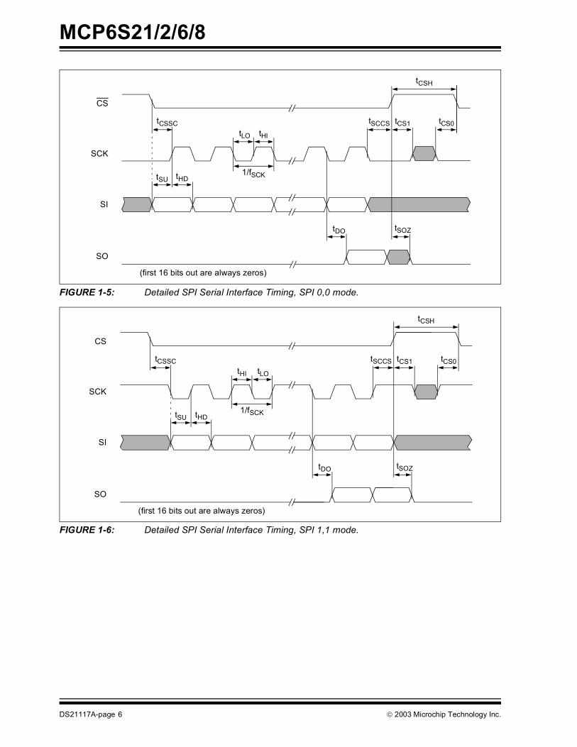
FIGURE 1-5: Detailed SPI Serial Interface Timing, SPI 0,0 mode.
FIGURE 1-6: Detailed SPI Serial Interface Timing, SPI 1,1 mode.
CS
SCK
SI
tSU tHD
tCSSC tSCCS
tCSH
SO
(first 16 bits out are always zeros)
tDO tSOZ
tLO tHI
1/fSCK
tCS0tCS1
CS
SCK
SI
tSU tHD
tCSSC tSCCS
SO
(first 16 bits out are always zeros)
tDO tSOZ
tHI tLO
1/fSCK
tCS1
tCSH
tCS0
DS21117A-page 6 2003 Microchip Technology Inc.
MCP6S21/2/6/8
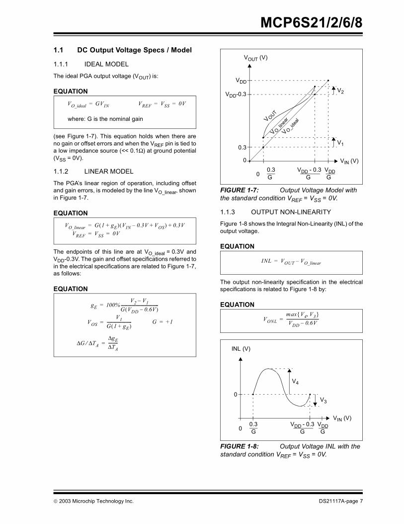
1.1 DC Output Voltage Specs / Model1.1.1 IDEAL MODEL
The ideal PGA output voltage (VOUT) is:
EQUATION
(see Figure 1-7). This equation holds when there areno gain or offset errors and when the VREF pin is tied toa low impedance source (<< 0.1Ω) at ground potential(VSS = 0V).
1.1.2 LINEAR MODEL
The PGA’s linear region of operation, including offsetand gain errors, is modeled by the line VO_linear, shownin Figure 1-7.
EQUATION
The endpoints of this line are at VO_ideal = 0.3V andVDD-0.3V. The gain and offset specifications referred toin the electrical specifications are related to Figure 1-7,as follows:
EQUATION
FIGURE 1-7: Output Voltage Model with the standard condition VREF = VSS = 0V.
1.1.3 OUTPUT NON-LINEARITY
Figure 1-8 shows the Integral Non-Linearity (INL) of theoutput voltage.
EQUATION
The output non-linearity specification in the electricalspecifications is related to Figure 1-8 by:
EQUATION
FIGURE 1-8: Output Voltage INL with the standard condition VREF = VSS = 0V.
VO_ideal GVIN= VREF VSS 0V= =
where: G is the nominal gain
VO_linear G 1 gE+( ) VIN 0.3V VOS+–( ) 0.3V+=VREF VSS 0V= =
gE 100%V2 V1–
G VDD 0.6V–( )--------------------------------------=
VOSV1
G 1 gE+( )-------------------------=
G TA∆⁄∆gE∆TA∆
----------=
G +1=
0
0
0.3
VDD-0.3
VDD
V OUT
VOUT (V)
VIN (V)0.3 VDD - 0.3 VDD
GG G
V1
V O_idea
l
V O_line
ar
V2
INL VOUT VO_linear–=
VONLmax V4 V3, VDD 0.6V–
---------------------------------=
0V3
V4
INL (V)
VIN (V)0.3 VDD - 0.3 VDD
GG G0
2003 Microchip Technology Inc. DS21117A-page 7
MCP6S21/2/6/8
1.1.4 DIFFERENT VREF CONDITIONSSome of the plots in Section 2.0, “Typical PerformanceCurves”, have the conditions VREF = VDD/2 orVREF = VDD. The equations and figures above are eas-ily modified for these conditions. The ideal VOUTbecomes:
EQUATION
The complete linear model is:
EQUATION
where the new VIN endpoints are:
EQUATION
The equations for extracting the specifications do notchange.
VO_ideal VREF G VIN VREF–( )+=
VDD VREF VSS> 0V=≥
VO_linear G 1 gE+( ) VIN VIN_L VOS+–( ) 0.3V+=
VIN_L0.3V VREF–
G VREF+------------------------------=
VIN_RVDD 0.3V– VREF–
G VREF+-----------------------------------------------=
DS21117A-page 8 2003 Microchip Technology Inc.
MCP6S21/2/6/8
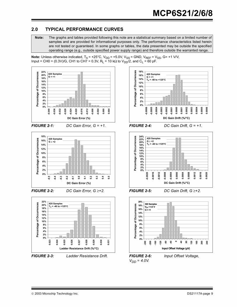
2.0 TYPICAL PERFORMANCE CURVESNote: Unless otherwise indicated, TA = +25°C, VDD = +5.0V, VSS = GND, VREF = VSS, G= +1 V/V, Input = CH0 = (0.3V)/G, CH1 to CH7 = 0.3V, RL = 10 kΩ to VDD/2, and CL = 60 pF.
FIGURE 2-1: DC Gain Error, G = +1.
FIGURE 2-2: DC Gain Error, G ≥+2.
FIGURE 2-3: Ladder Resistance Drift.
FIGURE 2-4: DC Gain Drift, G = +1.
FIGURE 2-5: DC Gain Drift, G ≥+2.
FIGURE 2-6: Input Offset Voltage, VDD = 4.0V.
Note: The graphs and tables provided following this note are a statistical summary based on a limited number ofsamples and are provided for informational purposes only. The performance characteristics listed hereinare not tested or guaranteed. In some graphs or tables, the data presented may be outside the specifiedoperating range (e.g., outside specified power supply range) and therefore outside the warranted range.
0%2%4%6%8%
10%12%14%16%18%20%22%
-0.0
40
-0.0
36
-0.0
32
-0.0
28
-0.0
24
-0.0
20
-0.0
16
-0.0
12
-0.0
08
-0.0
04
0.00
0
0.00
4
DC Gain Error (%)
Perc
enta
ge o
f Occ
urre
nces 420 Samples
G = +1
0%
2%
4%
6%
8%
10%
12%
14%
16%
18%
-0.5
-0.4
-0.3
-0.2
-0.1
0.0
0.1
0.2
0.3
0.4
0.5
DC Gain Error (%)
Pe
rce
nta
ge
of
Oc
cu
rre
nc
es 420 Samples
G +2
0%2%4%6%8%
10%12%14%16%18%20%22%
0.02
3
0.02
4
0.02
5
0.02
6
0.02
7
0.02
8
0.02
9
0.03
0
0.03
1
Ladder Resistance Drift (%/°C)
Perc
enta
ge o
f Occ
urre
nces 420 Samples
TA = -40 to +125°C
0%2%4%6%8%
10%12%14%16%18%
-0.0
006
-0.0
005
-0.0
004
-0.0
003
-0.0
002
-0.0
001
0.00
00
0.00
01
0.00
02
0.00
03
0.00
04
0.00
05
0.00
06
DC Gain Drift (%/°C)
Perc
enta
ge o
f Occ
urre
nces
420 SamplesG = +1TA = -40 to +125°C
0%
2%
4%
6%
8%
10%
12%
14%
16%
18%
20%
22%
24%
-0.0
020
-0.0
016
-0.0
012
-0.0
008
-0.0
004
0.0
000
0.0
004
0.0
008
0.0
012
0.0
016
0.0
020
DC Gain Drift (%/°C)
Perc
en
tag
e o
f O
ccu
rren
ces
420 Samples
G +2
TA = -40 to +125°C
0%2%4%6%8%
10%12%14%16%18%20%
-240
-200
-160
-120 -8
0
-40 0 40 80 120
160
200
240
Input Offset Voltage (µV)
Perc
enta
ge o
f Occ
urre
nces 360 Samples
VDD = 4.0 VG = +1
2003 Microchip Technology Inc. DS21117A-page 9

MCP6S21/2/6/8
Note: Unless otherwise indicated, TA = +25°C, VDD = +5.0V, VSS = GND, VREF = VSS, G= +1 V/V, Input = CH0 = (0.3V)/G, CH1 to CH7 = 0.3V, RL = 10 kΩ to VDD/2, and CL = 60 pF.FIGURE 2-7: Input Offset Voltage vs. VREF Voltage.
FIGURE 2-8: DC Output Non-Linearity vs. Supply Voltage.
FIGURE 2-9: Input Noise Voltage Density vs. Frequency.
FIGURE 2-10: Input Offset Voltage Drift.
FIGURE 2-11: DC Output Non-Linearity vs. Output Swing.
FIGURE 2-12: Input Noise Voltage Density vs. Gain.
-200
-150
-100
-50
0
50
100
150
200
0.0 0.5 1.0 1.5 2.0 2.5 3.0 3.5 4.0 4.5 5.0 5.5VREF Voltage (V)
Inpu
t Offs
et V
olta
ge (µ
V)
VDD = +5.5
VDD = +2.5
G = +1
0.00001
0.0001
0.001
0.01
2.5 3.0 3.5 4.0 4.5 5.0 5.5
Power Supply Voltage (V)
DC
Ou
tpu
t N
on
-Lin
eari
ty,
Inp
ut
Refe
rred
(%
of
FS
R)
VONL/G, G = +1
VONL/G, G = +2
VONL/G, G +4
VOUT = 0.3V to VDD -0.3V
1
10
100
1000
0.1 1 10 100 1000 10000 100000
Frequency (Hz)
Inp
ut
No
ise V
olt
ag
e D
en
sit
y
(nV
/H
z)
1k 10k 100k1 10 1000.1
0%2%4%6%8%
10%12%14%16%18%20%22%
-16
-14
-12
-10 -8 -6 -4 -2 0 2 4 6 8 10 12 14 16
Input Offset Voltage Drift (µV/°C)
Perc
enta
ge o
f Occ
urre
nces 420 Samples
TA = -40 to +125°CG = +1
0.0001%
0.0010%
0.0100%
1 10
Output Voltage Swing (VP-P)
DC
Ou
tpu
t N
on
-Lin
eari
ty,
Inp
ut
Refe
rred
(%
)
VONL/G, G +2
VONL/G, G = +1
VDD = +5.5 V
0
1
2
3
4
5
6
7
8
9
10
11
12
1 2 4 5 8 10 16 32
Gain (V/V)
Inp
ut
No
ise V
olt
ag
e D
en
sit
y
(nV
/H
z)
f = 10 kHz
DS21117A-page 10 2003 Microchip Technology Inc.
MCP6S21/2/6/8
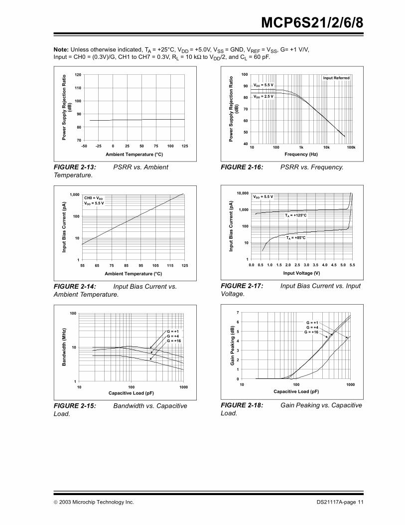
Note: Unless otherwise indicated, TA = +25°C, VDD = +5.0V, VSS = GND, VREF = VSS, G= +1 V/V, Input = CH0 = (0.3V)/G, CH1 to CH7 = 0.3V, RL = 10 kΩ to VDD/2, and CL = 60 pF.FIGURE 2-13: PSRR vs. Ambient Temperature.
FIGURE 2-14: Input Bias Current vs. Ambient Temperature.
FIGURE 2-15: Bandwidth vs. Capacitive Load.
FIGURE 2-16: PSRR vs. Frequency.
FIGURE 2-17: Input Bias Current vs. Input Voltage.
FIGURE 2-18: Gain Peaking vs. Capacitive Load.
70
80
90
100
110
120
-50 -25 0 25 50 75 100 125
Ambient Temperature (°C)
Pow
er S
uppl
y R
ejec
tion
Rat
io
(dB
)
1
10
100
1,000
55 65 75 85 95 105 115 125
Ambient Temperature (°C)
Inpu
t Bia
s C
urre
nt (p
A)
CH0 = VDD
VDD = 5.5 V
1
10
100
10 100 1000Capacitive Load (pF)
Ban
dwid
th (M
Hz) G = +1
G = +4G = +16
40
50
60
70
80
90
100
10 100 1000 10000 100000
Frequency (Hz)
Pow
er S
uppl
y R
ejec
tion
Rat
io
(dB
)
VDD = 2.5 V
VDD = 5.5 V
1k 10k 100k10 100
Input Referred
1
10
100
1,000
10,000
0.0 0.5 1.0 1.5 2.0 2.5 3.0 3.5 4.0 4.5 5.0 5.5
Input Voltage (V)
Inpu
t Bia
s C
urre
nt (p
A)
TA = +85°C
VDD = 5.5 V
TA = +125°C
0
1
2
3
4
5
6
7
10 100 1000
Capacitive Load (pF)
Gai
n Pe
akin
g (d
B)
G = +1G = +4
G = +16
2003 Microchip Technology Inc. DS21117A-page 11

MCP6S21/2/6/8
Note: Unless otherwise indicated, TA = +25°C, VDD = +5.0V, VSS = GND, VREF = VSS, G= +1 V/V, Input = CH0 = (0.3V)/G, CH1 to CH7 = 0.3V, RL = 10 kΩ to VDD/2, and CL = 60 pF.FIGURE 2-19: Gain vs. Frequency.
FIGURE 2-20: Histogram of Quiescent Current in Shutdown Mode.
FIGURE 2-21: Output Voltage Headroom vs. Output Current.
FIGURE 2-22: Quiescent Current vs. Supply Voltage.
FIGURE 2-23: Quiescent Current in Shutdown Mode vs. Ambient Temperature.
FIGURE 2-24: Output Short Circuit Current vs. Supply Voltage.
-20
-10
0
10
20
30
40
1.E+05 1.E+06 1.E+07 1.E+08
Frequency (Hz)
Gai
n (d
B)
G = +2G = +1
1M 10M 100M100k
G = +32G = +16
G = +10G = +8G = +5G = +4
0%10%20%30%40%50%60%70%80%90%
100%
0.0
0.1
0.2
0.3
0.4
0.5
0.6
0.7
0.8
0.9
1.0
Quiescent Current in Shutdown (µA)
Perc
enta
ge o
f Occ
urre
nces 420 Samples
VDD = 5.0 V
1
10
100
0.1 1 10Output Current Magnitude (mA)
Out
put V
olta
ge H
eadr
oom
(mV)
V DD
- V O
H an
d V O
L - V
SS
VDD = +5.5V
VDD = +2.5V
0.00.10.20.30.40.50.60.70.80.91.01.11.2
0.0 0.5 1.0 1.5 2.0 2.5 3.0 3.5 4.0 4.5 5.0 5.5
Supply Voltage (V)
Qui
esce
nt C
urre
nt (m
A)
TA = +125°CTA = +85°CTA = +25°CTA = -40°C
0.00.10.20.30.40.50.60.70.80.91.0
-50 -25 0 25 50 75 100 125Ambient Temperature (°C)
Qui
esce
nt C
urre
nt in
Shu
tdow
n (µ
A)
In Shutdown ModeVDD = 5.0 V
0
5
10
15
20
25
30
35
40
2.5 3.0 3.5 4.0 4.5 5.0 5.5Power Supply Voltage (V)
Out
put S
hort
Circ
uit C
urre
nt
(mA
)
TA = +125°CTA = +85°CTA = +25°CTA = -40°C
DS21117A-page 12 2003 Microchip Technology Inc.

MCP6S21/2/6/8
Note: Unless otherwise indicated, TA = +25°C, VDD = +5.0V, VSS = GND, VREF = VSS, G= +1 V/V, Input = CH0 = (0.3V)/G, CH1 to CH7 = 0.3V, RL = 10 kΩ to VDD/2, and CL = 60 pF.FIGURE 2-25: THD plus Noise vs. Frequency, VOUT = 2 VP-P.
FIGURE 2-26: Small Signal Pulse Response.
FIGURE 2-27: Channel Select Timing.
FIGURE 2-28: THD plus Noise vs. Frequency, VOUT = 4 VP-P.
FIGURE 2-29: Large Signal Pulse Response.
FIGURE 2-30: Gain Select Timing.
0.001
0.01
0.1
1
1.E+02 1.E+03 1.E+04 1.E+05
Frequency (Hz)
THD
+ N
oise
(%)
Measurement BW = 80 kHzVOUT = 2 VP-P
VDD = 5.0 V
100 1k 100k10k
G = +4
G = +1
G = +16
-40
-30
-20
-10
0
10
20
30
40
50
60
70
80
0.00E+00 2.00E-07 4.00E-07 6.00E-07 8.00E-07 1.00E-06 1.20E-06 1.40E-06 1.60E-06 1.80E-06 2.00E-06
Time (200 ns/div)
Out
put V
olta
ge(1
0 m
V/di
v)
-250
-200
-150
-100
-50
0
50
100
150
200
250
Nor
mal
ized
Inpu
t Vol
tage
(5
0 m
V/di
v)
VDD = +5.0V
VOUT, G = +1 G = +5 G = +32
GVIN
0.25
0.30
0.35
0.40
0.45
0.50
0.55
0.60
0.65
0.00E+00 5.00E-07 1.00E-06 1.50E-06 2.00E-06 2.50E-06 3.00E-06 3.50E-06 4.00E-06 4.50E-06 5.00E-06
Time (500 ns/div)
Out
put V
olta
ge (V
)
-20
-15
-10
-5
0
5
10
15
20
Chi
p Se
lect
Vol
tage
(V)
5
0
VOUT
(CH0 = 0.6V, G = +1)
VOUT(CH1 = 0.3V, G = +1)
CS
CS
0.001
0.01
0.1
1
1.E+02 1.E+03 1.E+04 1.E+05
Frequency (Hz)
THD
+ N
oise
(%)
Measurement BW = 80 kHzVOUT = 4 VP-P
VDD = 5.0 V
100 1k 100k10k
G = +4
G = +1
G = +16
0.0
0.5
1.0
1.5
2.0
2.5
3.0
3.5
4.0
4.5
5.0
0.00E+00 5.00E-07 1.00E-06 1.50E-06 2.00E-06 2.50E-06 3.00E-06 3.50E-06 4.00E-06 4.50E-06 5.00E-06
Time (500 ns/div)
Out
put V
olta
ge (V
)
-2.5
-1.5
-0.5
0.5
1.5
2.5
3.5
4.5
5.5
6.5
7.5
Nor
mal
ized
Inpu
t Vol
tage
(1V/
div)
VDD = +5.0V
GVINVOUT, G = +1 G = +5 G = +32
0.0
0.2
0.4
0.6
0.8
1.0
1.2
1.4
1.6
0.00E+00 5.00E-07 1.00E-06 1.50E-06 2.00E-06 2.50E-06 3.00E-06 3.50E-06 4.00E-06 4.50E-06 5.00E-06
Time (500 ns/div)
Out
put V
olta
ge (V
)
-20
-15
-10
-5
0
5
10
15
20
Chi
p Se
lect
Vol
tage
(V)
5
0
VOUT
(CH0 = 0.3V, G = +5)
VOUT
(CH0 = 0.3V, G = +1)
CS
CS
2003 Microchip Technology Inc. DS21117A-page 13
MCP6S21/2/6/8
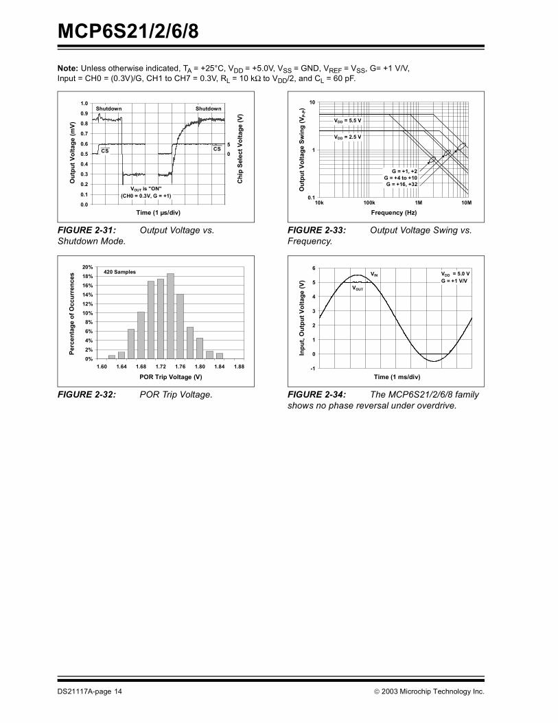
Note: Unless otherwise indicated, TA = +25°C, VDD = +5.0V, VSS = GND, VREF = VSS, G= +1 V/V, Input = CH0 = (0.3V)/G, CH1 to CH7 = 0.3V, RL = 10 kΩ to VDD/2, and CL = 60 pF.FIGURE 2-31: Output Voltage vs. Shutdown Mode.
FIGURE 2-32: POR Trip Voltage.
FIGURE 2-33: Output Voltage Swing vs. Frequency.
FIGURE 2-34: The MCP6S21/2/6/8 family shows no phase reversal under overdrive.
0.0
0.1
0.2
0.3
0.4
0.5
0.6
0.7
0.8
0.9
1.0
0.0E+00 1.0E-06 2.0E-06 3.0E-06 4.0E-06 5.0E-06 6.0E-06 7.0E-06 8.0E-06 9.0E-06 1.0E-05
Time (1 µs/div)
Out
put V
olta
ge (m
V)
-25
-20
-15
-10
-5
0
5
10
15
20
25
Chi
p Se
lect
Vol
tage
(V)
5
0
VOUT is "ON"(CH0 = 0.3V, G = +1)
Shutdown
CSCS
Shutdown
0%2%4%6%8%
10%12%14%16%18%20%
1.60 1.64 1.68 1.72 1.76 1.80 1.84 1.88
POR Trip Voltage (V)
Perc
enta
ge o
f Occ
urre
nces
420 Samples
0.1
1
10
1.E+04 1.E+05 1.E+06 1.E+07
Frequency (Hz)
Out
put V
olta
ge S
win
g (V
P-P)
VDD = 2.5 V
VDD = 5.5 V
G = +1, +2G = +4 to +10G = +16, +32
10k 100k 10M1M
-1
0
1
2
3
4
5
6
0.0E+00 1.0E-03 2.0E-03 3.0E-03 4.0E-03 5.0E-03 6.0E-03 7.0E-03 8.0E-03 9.0E-03 1.0E-02
Time (1 ms/div)
Inpu
t, O
utpu
t Vol
tage
(V)
VDD = 5.0 VG = +1 V/V
VIN
VOUT
DS21117A-page 14 2003 Microchip Technology Inc.
MCP6S21/2/6/8
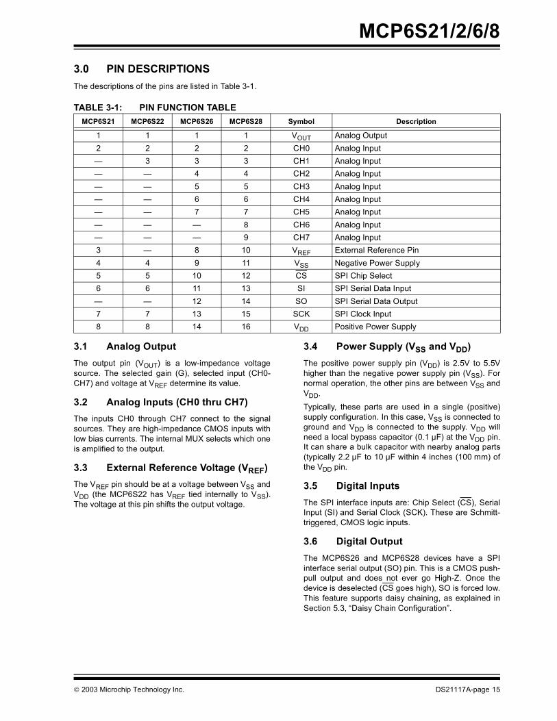
3.0 PIN DESCRIPTIONSThe descriptions of the pins are listed in Table 3-1.TABLE 3-1: PIN FUNCTION TABLE
3.1 Analog OutputThe output pin (VOUT) is a low-impedance voltagesource. The selected gain (G), selected input (CH0-CH7) and voltage at VREF determine its value.
3.2 Analog Inputs (CH0 thru CH7)The inputs CH0 through CH7 connect to the signalsources. They are high-impedance CMOS inputs withlow bias currents. The internal MUX selects which oneis amplified to the output.
3.3 External Reference Voltage (VREF)The VREF pin should be at a voltage between VSS andVDD (the MCP6S22 has VREF tied internally to VSS).The voltage at this pin shifts the output voltage.
3.4 Power Supply (VSS and VDD)The positive power supply pin (VDD) is 2.5V to 5.5Vhigher than the negative power supply pin (VSS). Fornormal operation, the other pins are between VSS andVDD.Typically, these parts are used in a single (positive)supply configuration. In this case, VSS is connected toground and VDD is connected to the supply. VDD willneed a local bypass capacitor (0.1 µF) at the VDD pin.It can share a bulk capacitor with nearby analog parts(typically 2.2 µF to 10 µF within 4 inches (100 mm) ofthe VDD pin.
3.5 Digital InputsThe SPI interface inputs are: Chip Select (CS), SerialInput (SI) and Serial Clock (SCK). These are Schmitt-triggered, CMOS logic inputs.
3.6 Digital OutputThe MCP6S26 and MCP6S28 devices have a SPIinterface serial output (SO) pin. This is a CMOS push-pull output and does not ever go High-Z. Once thedevice is deselected (CS goes high), SO is forced low.This feature supports daisy chaining, as explained inSection 5.3, “Daisy Chain Configuration”.
MCP6S21 MCP6S22 MCP6S26 MCP6S28 Symbol Description
1 1 1 1 VOUT Analog Output2 2 2 2 CH0 Analog Input— 3 3 3 CH1 Analog Input— — 4 4 CH2 Analog Input— — 5 5 CH3 Analog Input— — 6 6 CH4 Analog Input— — 7 7 CH5 Analog Input— — — 8 CH6 Analog Input— — — 9 CH7 Analog Input3 — 8 10 VREF External Reference Pin4 4 9 11 VSS Negative Power Supply5 5 10 12 CS SPI Chip Select6 6 11 13 SI SPI Serial Data Input— — 12 14 SO SPI Serial Data Output7 7 13 15 SCK SPI Clock Input8 8 14 16 VDD Positive Power Supply
2003 Microchip Technology Inc. DS21117A-page 15

MCP6S21/2/6/8
4.0 ANALOG FUNCTIONSThe MCP6S21/2/6/8 family of Programmable GainAmplifiers (PGA) are based on simple analog buildingblocks (see Figure 4-1). Each of these blocks will beexplained in more detail in the following sub-sections.FIGURE 4-1: PGA Block Diagram.
4.1 Input MUXThe MCP6S21 has one input, the MCP6S22 andMCP6S25 have two inputs, the MCP6S26 has sixinputs and the MCP6S28 has eight inputs (seeFigure 4-1).For the lowest input current, float unused inputs. Tyingthese pins to a voltage near the used channels alsoworks well. For simplicity, they can be tied to VSS orVDD, but the input current may increase.The one channel MCP6S21 has the lowest input biascurrent, while the eight channel MCP6S28 has thehighest. There is about a 2:1 ratio in IB between theseparts.
4.2 Internal Op AmpThe internal op amp provides the right combination ofbandwidth, accuracy and flexibility.
4.2.1 COMPENSATION CAPACITORS
The internal op amp has three compensation capaci-tors connected to a switching network. They areselected to give good small signal bandwidth at highgains, and good slew rate (full power bandwidth) at lowgains. The change in bandwidth as gain changes isbetween 2 MHz and 12 MHz. Refer to Table 4-1 formore information.
TABLE 4-1: GAIN VS. INTERNAL COMPENSATION CAPACITOR
MCP6S21–One input (CH0), no SO pin MCP6S22–Two inputs (CH0, CH1), VREF tied internallyto VSS, no SO pinMCP6S26–Six inputs (CH0 to CH5)MCP6S28–Eight inputs (CH0 to CH7)
VOUT
VREF
VDD
CSSI
SOSCK
CH1CH0
CH3CH2
CH5CH4
CH7CH6
VSS
8RF
RG
MUX
SPI™Logic
POR
GainSwitches
+
- Resistor Ladder (R
LAD )
Gain(V/V)
Internal Compensation
Capacitor
Typical GBWP (MHz)
Typical SR(V/µs)
Typical FPBW (MHz)
Typical BW(MHz)
1 Large 12 4.0 0.30 122 Large 12 4.0 0.30 64 Medium 20 11 0.70 105 Medium 20 11 0.70 78 Medium 20 11 0.70 2.4
10 Medium 20 11 0.70 2.016 Small 64 22 1.6 532 Small 64 22 1.6 2.0
Note 1: FPBW is the Full Power Bandwidth. These numbers are based on VDD = 5.0V.2: No changes in DC performance (e.g., VOS) accompany a change in compensation capacitor.3: BW is the closed-loop, small signal -3 dB bandwidth.
DS21117A-page 16 2003 Microchip Technology Inc.
MCP6S21/2/6/8
4.2.2 RAIL-TO-RAIL INPUTThe input stage of the internal op amp uses two differ-ential input stages in parallel; one operates at low VIN(input voltage), while the other operates at high VIN.With this topology, the internal inputs can operate to0.3V past either supply rail. The input offset voltage ismeasured at both VIN = VSS - 0.3V and VDD + 0.3V toensure proper operation.The transition between the two input stages occurswhen VIN ≈ VDD - 1.5V. For the best distortion and gainlinearity, avoid this region of operation.
4.2.3 RAIL-TO-RAIL OUTPUT
The Maximum Output Voltage Swing is the maximumswing possible under a particular output load. Accord-ing to the specification table, the output can reachwithin 60 mV of either supply rail when RL = 10 kΩ andVREF = VDD/2. See Figure 2-21 for typical performanceunder other conditions.
4.2.4 INPUT VOLTAGE AND PHASE REVERSAL
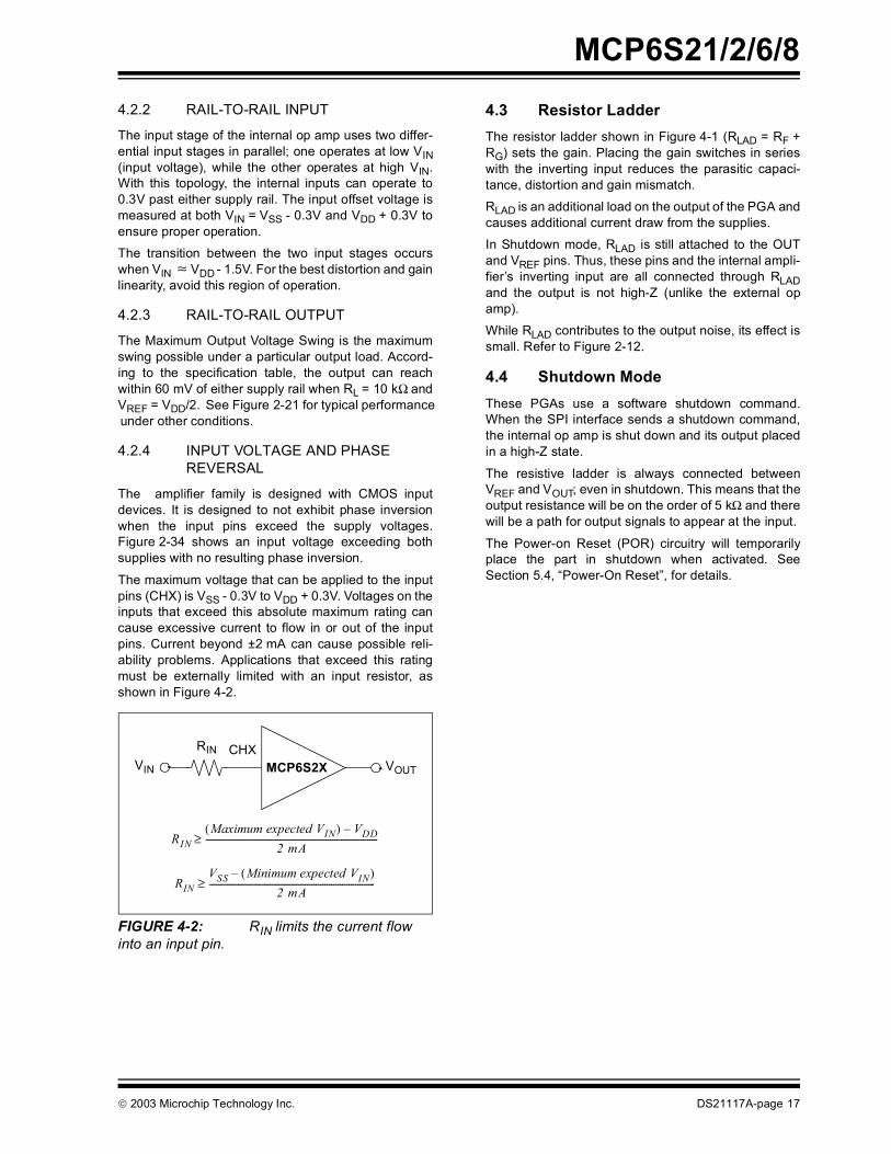
The amplifier family is designed with CMOS inputdevices. It is designed to not exhibit phase inversionwhen the input pins exceed the supply voltages.Figure 2-34 shows an input voltage exceeding bothsupplies with no resulting phase inversion.
The maximum voltage that can be applied to the inputpins (CHX) is VSS - 0.3V to VDD + 0.3V. Voltages on theinputs that exceed this absolute maximum rating cancause excessive current to flow in or out of the inputpins. Current beyond ±2 mA can cause possible reli-ability problems. Applications that exceed this ratingmust be externally limited with an input resistor, asshown in Figure 4-2.
FIGURE 4-2: RIN limits the current flow into an input pin.
4.3 Resistor LadderThe resistor ladder shown in Figure 4-1 (RLAD = RF +RG) sets the gain. Placing the gain switches in serieswith the inverting input reduces the parasitic capaci-tance, distortion and gain mismatch.RLAD is an additional load on the output of the PGA andcauses additional current draw from the supplies.In Shutdown mode, RLAD is still attached to the OUTand VREF pins. Thus, these pins and the internal ampli-fier’s inverting input are all connected through RLADand the output is not high-Z (unlike the external opamp).While RLAD contributes to the output noise, its effect issmall. Refer to Figure 2-12.
4.4 Shutdown ModeThese PGAs use a software shutdown command.When the SPI interface sends a shutdown command,the internal op amp is shut down and its output placedin a high-Z state.
The resistive ladder is always connected betweenVREF and VOUT; even in shutdown. This means that theoutput resistance will be on the order of 5 kΩ and therewill be a path for output signals to appear at the input.
The Power-on Reset (POR) circuitry will temporarilyplace the part in shutdown when activated. SeeSection 5.4, “Power-On Reset”, for details.
RINVSS Minimum expected VIN( )–
2 mA----------------------------------------------------------------------------≥
RINMaximum expected VIN( ) VDD–
2 mA-------------------------------------------------------------------------------≥
VIN
RINVOUTMCP6S2X
CHX
2003 Microchip Technology Inc. DS21117A-page 17

MCP6S21/2/6/8
5.0 DIGITAL FUNCTIONSThe MCP6S21/2/6/8 PGAs use a standard SPI com-patible serial interface to receive instructions from acontroller. This interface is configured to allow daisychaining with other SPI devices. There is an internalPOR (Power On Reset) that resets the registers underlow power conditions.5.1 SPI TimingChip Select (CS) toggles low to initiate communicationwith these devices. The first byte of each SI word (twobytes long) is the instruction byte, which goes into theInstruction Register. The Instruction Register points thesecond byte to its destination. In a typical application,
CS is raised after one word (16 bits) to implement thedesired changes. Section 5.3, “Registers”, coversapplications using multiple 16-bit words. SO goes lowafter CS goes high; it has a push-pull output that doesnot go into a high-Z state.
The MCP6S21/2/6/8 devices operate in SPI Modes 0,0and 1,1. In 0,0 mode, the clock idles in the low state(Figure 5-1) and, in 1,1 mode, the clock idles in the highstate (Figure 5-2). In both modes, SI data is loaded intothe PGA on the rising edge of SCK and SO data isclocked out on the falling edge of SCK. In 0,0 mode, thefalling edge of CS also acts as the first falling edge ofSCK (see Figure 5-1). There must be multiples of 16clocks (SCK) while CS is low or commands will abort(see Section 5.3, “Registers”).
FIGURE 5-1: Serial bus sequence for the PGA; SPI 0,0 mode (see Figure 1-5).
FIGURE 5-2: Serial bus sequence for the PGA; SPI 1,1 mode (see Figure 1-6).
1 2 3 4 5 6 7 8 9 10 11 12 13 14 15 16
bit 7
CS
SCK
SI
Instruction Byte Data Byte
bit 0
bit 7
bit 0
SO
(first 16 bits out are always zeros)
1 2 3 4 5 6 7 8 9 10 11 12 13 14 15 16
bit 7
CS
SCK
SI
Instruction Byte Data Byte
bit 0
bit 7
bit 0
SO
(first 16 bits out are always zeros)
DS21117A-page 18 2003 Microchip Technology Inc.
MCP6S21/2/6/8
5.2 RegistersThe analog functions are programmed through the SPIinterface using 16-bit words (see Figure 5-1 andFigure 5-2). This data is sent to two of three 8-bit regis-ters: Instruction Register (Register 5-1), Gain Register(Register 5-2) and Channel Register (Register 5-3).The power-up defaults for these three registers are:• Instruction Register: 000x xxx0• Gain Register: xxxx x000• Channel Register: xxxx x000
Thus, these devices are initially programmed with theInstruction Register set for NOP (no operation), a gainof +1 V/V and CH0 as the input channel.
5.2.1 INSTRUCTION REGISTER
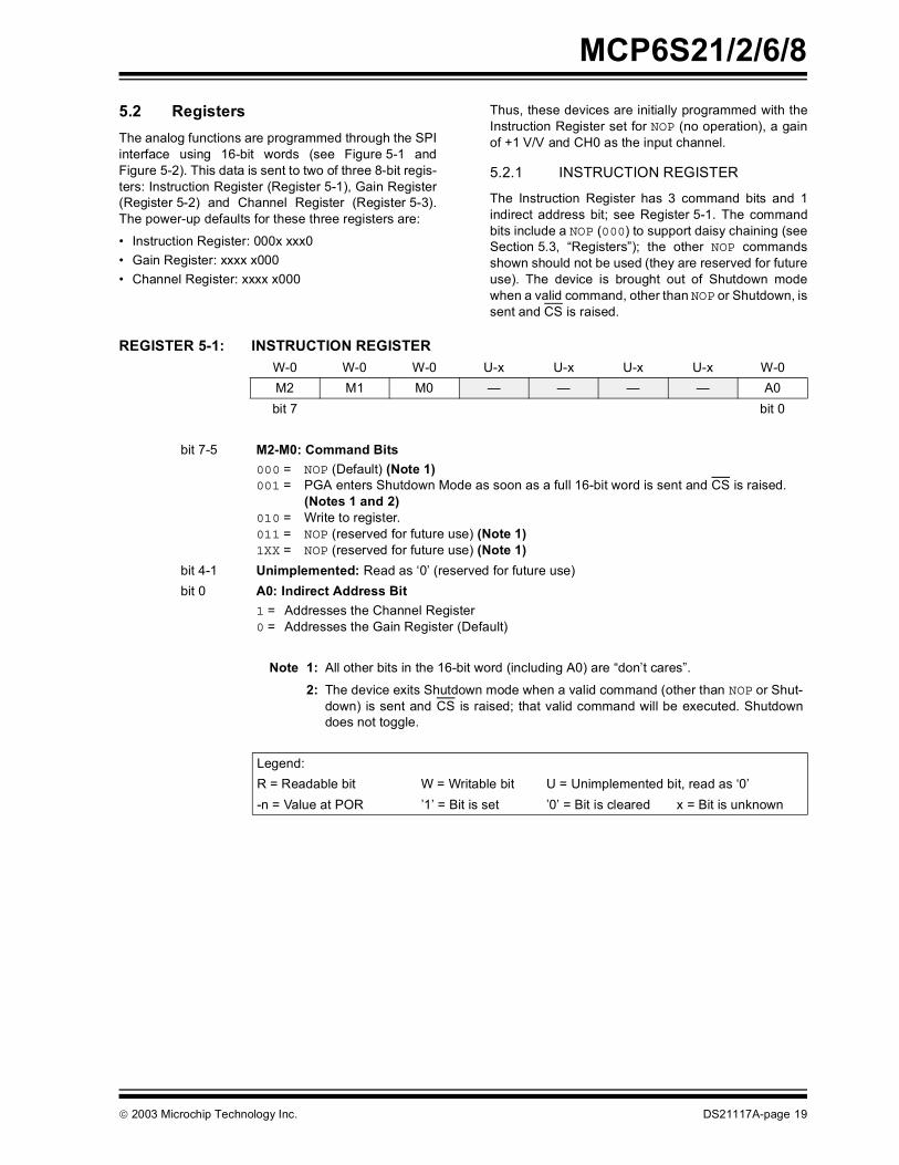
The Instruction Register has 3 command bits and 1indirect address bit; see Register 5-1. The commandbits include a NOP (000) to support daisy chaining (seeSection 5.3, “Registers”); the other NOP commandsshown should not be used (they are reserved for futureuse). The device is brought out of Shutdown modewhen a valid command, other than NOP or Shutdown, issent and CS is raised.
REGISTER 5-1: INSTRUCTION REGISTERW-0 W-0 W-0 U-x U-x U-x U-x W-0M2 M1 M0 — — — — A0bit 7 bit 0
bit 7-5 M2-M0: Command Bits000 = NOP (Default) (Note 1)001 = PGA enters Shutdown Mode as soon as a full 16-bit word is sent and CS is raised.
(Notes 1 and 2)010 = Write to register.011 = NOP (reserved for future use) (Note 1)1XX = NOP (reserved for future use) (Note 1)
bit 4-1 Unimplemented: Read as ‘0’ (reserved for future use)bit 0 A0: Indirect Address Bit
1 = Addresses the Channel Register0 = Addresses the Gain Register (Default)
Note 1: All other bits in the 16-bit word (including A0) are “don’t cares”.
2: The device exits Shutdown mode when a valid command (other than NOP or Shut-down) is sent and CS is raised; that valid command will be executed. Shutdowndoes not toggle.
Legend:R = Readable bit W = Writable bit U = Unimplemented bit, read as ‘0’-n = Value at POR ’1’ = Bit is set ’0’ = Bit is cleared x = Bit is unknown
2003 Microchip Technology Inc. DS21117A-page 19
MCP6S21/2/6/8
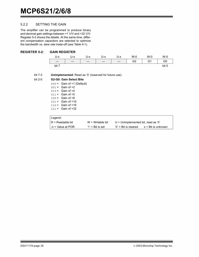
5.2.2 SETTING THE GAINThe amplifier can be programmed to produce binaryand decimal gain settings between +1 V/V and +32 V/V.Register 5-2 shows the details. At the same time, differ-ent compensation capacitors are selected to optimizethe bandwidth vs. slew rate trade-off (see Table 4-1).
REGISTER 5-2: GAIN REGISTERU-x U-x U-x U-x U-x W-0 W-0 W-0— — — — — G2 G1 G0
bit 7 bit 0
bit 7-3 Unimplemented: Read as ‘0’ (reserved for future use)bit 2-0 G2-G0: Gain Select Bits
000 = Gain of +1 (Default)001 = Gain of +2010 = Gain of +4011 = Gain of +5100 = Gain of +8101 = Gain of +10110 = Gain of +16111 = Gain of +32
Legend:R = Readable bit W = Writable bit U = Unimplemented bit, read as ‘0’-n = Value at POR ’1’ = Bit is set ’0’ = Bit is cleared x = Bit is unknown
DS21117A-page 20 2003 Microchip Technology Inc.

MCP6S21/2/6/8
5.2.3 CHANGING THE CHANNELIf the instruction register is programmed to address thechannel register, the multiplexed inputs of theMCP6S22, MCP6S26 and MCP6S28 can be changedper Register 5-3.
REGISTER 5-3: CHANNEL REGISTERU-x U-x U-x U-x U-x W-0 W-0 W-0— — — — — C2 C1 C0
bit 7 bit 0
bit 7-3 Unimplemented: Read as ‘0’ (reserved for future use)bit 2-0 C2-C0: Channel Select Bits
MCP6S21000 = CH0 (Default)001 = CH0001 = CH0011 = CH0100 = CH0101 = CH0110 = CH0111 = CH0
MCP6S22CH0 (Default)CH1CH0CH1CH0CH1CH0CH1
MCP6S26CH0 (Default)CH1CH2CH3CH4CH5CH0CH0
MCP6S28CH0 (Default)CH1CH2CH3CH4CH5CH6CH7
Legend:R = Readable bit W = Writable bit U = Unimplemented bit, read as ‘0’-n = Value at POR ’1’ = Bit is set ’0’ = Bit is cleared x = Bit is unknown
2003 Microchip Technology Inc. DS21117A-page 21

MCP6S21/2/6/8
5.2.4 SHUTDOWN COMMANDThe software Shutdown command allows the user toput the amplifier into a low power mode (seeRegister 5-1). In this shutdown mode, most pins arehigh impedance (Section 4.4, “Shutdown Mode”, andSection 5.1, “SPI Timing”, cover the exceptions at pinsVREF, VOUT and SO).
Once the PGA has entered shutdown mode, it willremain in this mode until either a valid command is sentto the device (other than NOP or Shutdown), or thedevice is powered down and back up again. Theinternal registers maintain their values while inshutdown.Once brought out of shutdown mode, the part comesback to its previous state (see Section 5.4 for excep-tions to this rule). This makes it possible to bring thedevice out of shutdown mode using one command;send a command to select the current channel (or gain)and the device will exit shutdown with the same statethat existed before shutdown.
5.3 Daisy Chain ConfigurationMultiple devices can be connected in a daisy chainconfiguration by connecting the SO pin from one deviceto the SI pin on the next device and using common SCKand CS lines (Figure 5-3). This approach reduces PCBlayout complexity.
The example in Figure 5-3 shows a daisy chain config-uration with two devices, although any number ofdevices can be configured this way. The MCP6S21 andMCP6S22 can only be used at the far end of the daisychain because they do not have a serial data out (SO)pin. As shown in Figure 5-4 and Figure 5-5, both SIand SO data are sent in 16-bit (2 byte) words. Thesedevices abort any command that is not a multiple of 16bits.When using the daisy chain configuration, the maxi-mum clock speed possible is reduced to ≈ 5.8 MHzbecause of the SO pin’s propagation delay (seeElectrical Specifications).The internal SPI shift register is automatically loadedwith zeros whenever CS goes high (a command is exe-cuted). Thus, the first 16-bits out of the SO pin once CSline goes low are always zeros. This means that thefirst command loaded into the next device in the daisychain is a NOP. This feature makes it possible to sendshorter command and data byte strings when the far-thest devices do not need to change. For example, ifthere were three devices on the chain and only the mid-dle device needed changing, only 32 bytes of dataneed to be transmitted (for the first and middledevices), and the last device on the chain wouldreceive a NOP when the CS pin is raised to execute thecommand.
FIGURE 5-3: Daisy Chain Configuration.
MicrocontrollerSO
CSSCKSI
CSSCK
SO
Device 1
Device 100100000 00000000
SO
CSSCKSIDevice 2
Device 200000000 00000000
1. Set CS low.2. Clock out the instruction and data
for Device 2 (16 clocks) to Device 1.3. Device 1 automatically clocks out all
zeros (first 16 clocks) to Device 2.
4. Clock out the instruction and datafor Device 1 (16 clocks) to Device 1.
5. Device 1 automatically shifts datafrom Device 1 to Device 2 (16clocks).
6. Raise CS.
Device 101000001 00000111
Device 200100000 00000000
PICmicro®
DS21117A-page 22 2003 Microchip Technology Inc.
MCP6S21/2/6/8
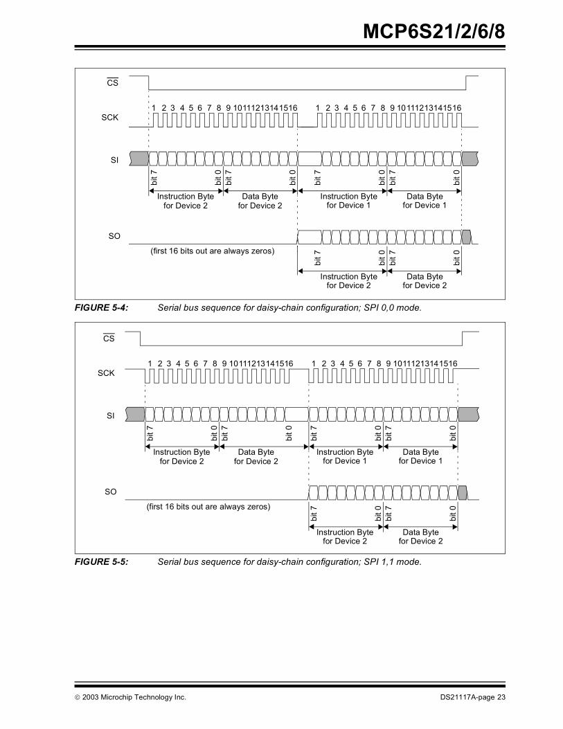
FIGURE 5-4: Serial bus sequence for daisy-chain configuration; SPI 0,0 mode.
FIGURE 5-5: Serial bus sequence for daisy-chain configuration; SPI 1,1 mode.
1 2 3 4 5 6 7 8 9 10111213141516
bit 7
CS
SCK
SI
Instruction Byte Data Byte
bit 0
bit 7
bit 0
SO
(first 16 bits out are always zeros)
1 2 3 4 5 6 7 8 9 10111213141516
bit 7
Instruction Byte Data Byte
bit 0
bit 7
bit 0
for Device 2 for Device 2 for Device 1 for Device 1
bit 7
Instruction Byte Data Byte
bit 0
bit 7
bit 0
for Device 2 for Device 2
1 2 3 4 5 6 7 8 9 10111213141516
bit 7
CS
SCK
SI
Instruction Byte Data Byte
bit 0
bit 7
bit 0
SO
(first 16 bits out are always zeros)
1 2 3 4 5 6 7 8 9 10111213141516
bit 7
Instruction Byte Data Byte
bit 0
bit 7
bit 0
for Device 2 for Device 2 for Device 1 for Device 1
bit 7
Instruction Byte Data Byte
bit 0
bit 7
bit 0
for Device 2 for Device 2
2003 Microchip Technology Inc. DS21117A-page 23

MCP6S21/2/6/8
5.4 Power-On ResetIf the power supply voltage goes below the POR tripvoltage (VDD < VPOR ≈ 1.7V), the internal POR circuitwill reset all of the internal registers to their power-updefaults (this is a protection against low power supplyvoltages). The POR circuit also holds the part in shut-down mode while it is activated. It temporarily overridesthe software shutdown status. The POR releases theshutdown circuitry once it is released (VDD > VPOR).A 0.1 µF bypass capacitor mounted as close as possi-ble to the VDD pin provides additional transientimmunity.DS21117A-page 24 2003 Microchip Technology Inc.

MCP6S21/2/6/8
6.0 APPLICATIONS INFORMATION6.1 Changing External Reference Voltage
Figure 6-1 shows a MCP6S21 with the VREF pin at2.5V and VDD = 5.0V. This allows the PGA to amplifysignals centered on 2.5V, instead of ground-referencedsignals. The voltage reference MCP1525 is buffered bya MCP6021, which gives a low output impedance ref-erence voltage from DC to high frequencies. Thesource driving the VREF pin should have an outputimpedance of ≤ 0.1Ω to maintain reasonable gainaccuracy.
FIGURE 6-1: PGA with Different External Reference Voltage.
6.2 Capacitive Load and StabilityLarge capacitive loads can cause both stability prob-lems and reduced bandwidth for the MCP6S21/2/6/8family of PGAs (Figure 2-17 and Figure 2-18). Thishappens because a large load capacitance decreasesthe internal amplifier’s phase margin and bandwidth.
If the PGA drives a large capacitive load, the circuit inFigure 6-2 can be used. A small series resistor (RISO)at the VOUT improves the phase margin by making theload resistive at high frequencies. It will not, however,improve the bandwidth.
FIGURE 6-2: PGA Circuit for Large Capacitive Loads.
For CL ≥ 100 pF, a good estimate for RISO is 50Ω. Thisvalue can be fine-tuned on the bench. Adjust RISO sothat the step response overshoot and frequencyresponse peaking are acceptable at all gains.
6.3 Layout ConsiderationsGood PC board layout techniques will help achieve theperformance shown in the Electrical Characteristicsand Typical Performance Curves. It will also helpminimize EMC (Electro-Magnetic Compatibility) issues.
6.3.1 COMPONENT PLACEMENT
Separate circuit functions; digital from analog, lowspeed from high speed, and low power from highpower, as this will reduce crosstalk.
Keep sensitive traces short and straight, separatingthem from interfering components and traces. This isespecially important for high frequency (low rise time)signals.
Use a 0.1 µF supply bypass capacitor within 0.1 inch(2.5 mm) of the VDD pin. It must connect directly to theground plane. A multi-layer ceramic chip capacitor, orhigh-frequency equivalent, works best.
6.3.2 SIGNAL COUPLING
The input pins of the MCP6S21/2/6/8 family of opera-tional amplifiers (op amps) are high-impedance. Thismakes them especially susceptible to capacitively-cou-pled noise. Using a ground plane helps reduce thisproblem.
When noise is capacitively-coupled, the ground planeprovides additional shunt capacitance to ground. Whennoise is magnetically coupled, the ground planereduces the mutual inductance between traces.Increasing the separation between traces makes asignificant difference.Changing the direction of one of the traces can alsoreduce magnetic coupling. It may help to locate guardtraces next to the victim trace. They should be on bothsides of the victim trace and be as close as possible.Connect the guard traces to the ground plane at bothends, and in the middle, of long traces.
6.3.3 HIGH FREQUENCY ISSUES
Because the MCP6S21/2/6/8 PGAs reach unity gainnear 64 MHz when G = 16 and 32, it is important to usegood PCB layout techniques. Any parasitic coupling athigh frequency might cause undesired peaking. Filter-ing high frequency signals (i.e., fast edge rates) canhelp. To minimize high frequency problems:
• Use complete ground and power planes• Use HF, surface mount components• Provide clean supply voltages and bypassing• Keep traces short and straight• Try a linear power supply (e.g., an LDO)
VDD
VREF
MCP6S21MCP1525
MCP6021
2.5VREF
VDD
VDD
VIN VOUT
1 µF
VIN MCP6S2XRISO
VOUT
CL
2003 Microchip Technology Inc. DS21117A-page 25

MCP6S21/2/6/8
6.4 Typical Applications6.4.1 GAIN RANGING
Figure 6-3 shows a circuit that measures the current IX.It benefits from changing the gain on the PGA. Just asa hand-held multimeter uses different measurementranges to obtain the best results, this circuit makes iteasy to set a high gain for small signals and a low gainfor large signals. As a result, the required dynamicrange at the PGA’s output is less than at its input (by upto 30 dB).
FIGURE 6-3: Wide Dynamic Range Current Measurement Circuit.
6.4.2 SHIFTED GAIN RANGE PGA
Figure 6-4 shows a circuit using an MCP6021 at a gainof +10 in front of an MCP6S21. This changes the over-all gain range to +10 V/V to +320 V/V (from +1 V/V to+32 V/V).
FIGURE 6-4: PGA with Modified Gain Range.It is also easy to shift the gain range to lower gains (seeFigure 6-6). The MCP6021 acts as a unity gain buffer,and the resistive voltage divider shifts the gain rangedown to +0.1 V/V to +3.2 V/V (from +1 V/V to +32 V/V).
FIGURE 6-5: PGA with lower gain range.
6.4.3 EXTENDED GAIN RANGE PGA
Figure 6-6 gives a +1 V/V to +1024 V/V gain range,which is much greater than the range for a single PGA(+1 V/V to +32 V/V). The first PGA provides input mul-tiplexing capability, while the second PGA only needsone input. These devices can be daisy chained(Section 5.3, “Daisy Chain Configuration”).
FIGURE 6-6: PGA with Extended Gain Range.
6.4.4 MULTIPLE SENSOR AMPLIFIER
The multiple channel PGAs (except the MCP6S21)allow the user to select which sensor appears on theoutput (see Figure 6-7). These devices can alsochange the gain to optimize performance for eachsensor.
FIGURE 6-7: PGA with Multiple Sensor Inputs.
MCP6S2X VOUT
IX RS
VIN
MCP6021 MCP6S21 VOUT
10.0 kΩ1.11 kΩ
+
_
VIN
MCP6021
MCP6S21VOUT
10.0 kΩ
1.11 kΩ
+
_
VIN VOUTMCP6S28 MCP6S21
Sensor # 0Sensor # 1
Sensor # 5
MCP6S26 VOUT
DS21117A-page 26 2003 Microchip Technology Inc.
MCP6S21/2/6/8
6.4.5 EXPANDED INPUT PGAFigure 6-8 shows cascaded MCP6S28s that provideup to 15 input channels. Obviously, Sensors #7-14have a high total gain range available, as explained inSection 6.4.3, “Extended Gain Range”. These devicescan be daisy chained (Section 5.3, “Daisy ChainConfiguration”).
FIGURE 6-8: PGA with Expanded Inputs.
6.4.6 PICmicro® MCU WITH EXPANDED INPUT CAPABILITY
Figure 6-9 shows an MCP6S28 driving an analog inputto a PICmicro® microcontroller. This greatly expandsthe input capacity of the microcontroller, while addingthe ability to select the appropriate gain for eachsource.
FIGURE 6-9: Expanded Input for a PICmicro Microcontroller.
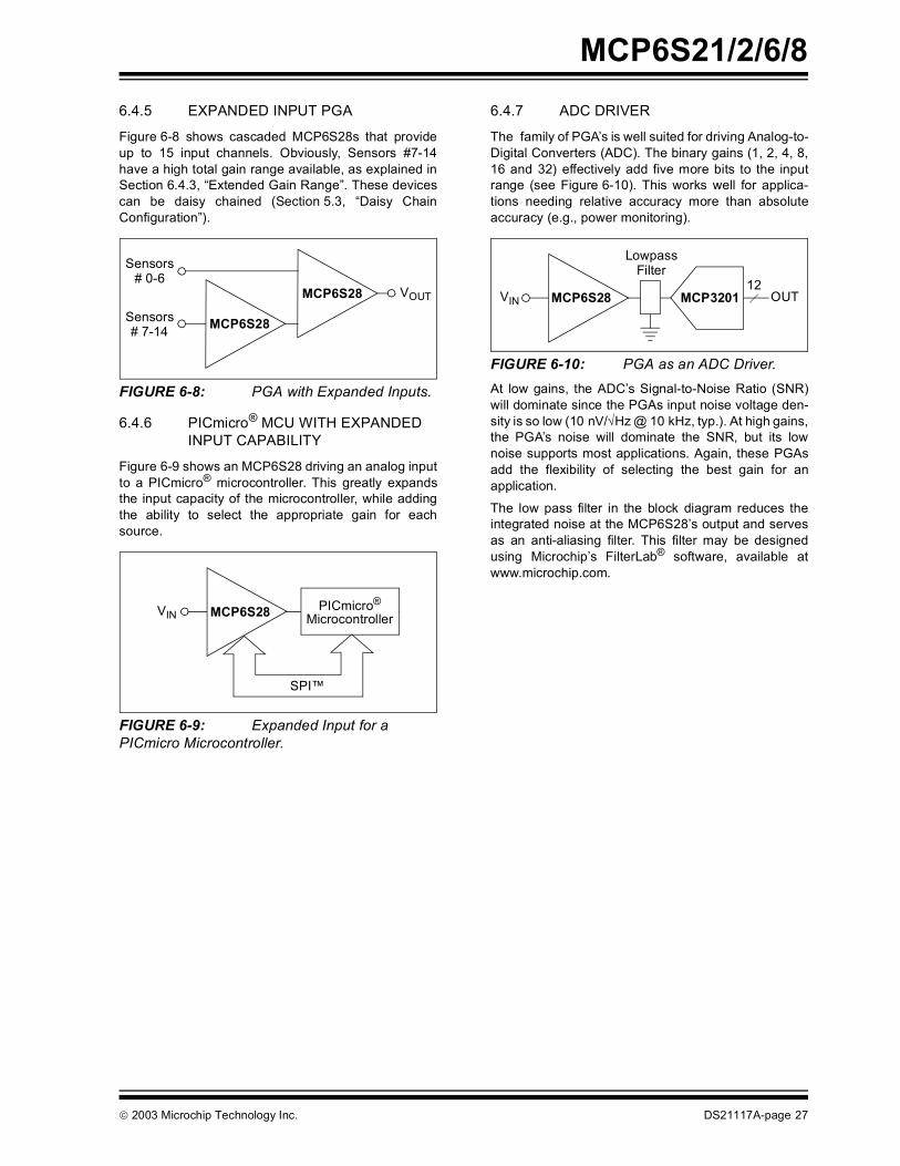
6.4.7 ADC DRIVER
The family of PGA’s is well suited for driving Analog-to-Digital Converters (ADC). The binary gains (1, 2, 4, 8,16 and 32) effectively add five more bits to the inputrange (see Figure 6-10). This works well for applica-tions needing relative accuracy more than absoluteaccuracy (e.g., power monitoring).
FIGURE 6-10: PGA as an ADC Driver. At low gains, the ADC’s Signal-to-Noise Ratio (SNR)will dominate since the PGAs input noise voltage den-sity is so low (10 nV/√Hz @ 10 kHz, typ.). At high gains,the PGA’s noise will dominate the SNR, but its lownoise supports most applications. Again, these PGAsadd the flexibility of selecting the best gain for anapplication.
The low pass filter in the block diagram reduces theintegrated noise at the MCP6S28’s output and servesas an anti-aliasing filter. This filter may be designedusing Microchip’s FilterLab® software, available atwww.microchip.com.
Sensors
Sensors MCP6S28
MCP6S28 VOUT# 0-6
# 7-14
VIN MCP6S28 PICmicro®
Microcontroller
SPI™
VIN OUTMCP6S28
LowpassFilter
12MCP3201
2003 Microchip Technology Inc. DS21117A-page 27

MCP6S21/2/6/8
7.0 PACKAGING INFORMATION7.1 Package Marking Information
XXXXXXXXXXXXXNNN
YYWW
8-Lead PDIP (300 mil) (MCP6S21, MCP6S22) Example:
8-Lead SOIC (150 mil) (MCP6S21, MCP6S22) Example:
XXXXXXXXXXXXYYWW
NNN
MCP6S21I/P256
0345
MCP6S21I/SN0345
256
8-Lead MSOP (MCP6S21, MCP6S22) Example:
XXXXX
YWWNNN
MCP6S21I
345256
Legend: XX...X Customer specific information*YY Year code (last 2 digits of calendar year)WW Week code (week of January 1 is week ‘01’)NNN Alphanumeric traceability code
Note: In the event the full Microchip part number cannot be marked on one line, it will be carried over to the next line thus limiting the number of available characters for customer specific information.
* Standard marking consists of Microchip part number, year code, week code, traceability code (facility code, mask rev#, and assembly code). For marking beyond this, certain price adders apply. Please check with your Microchip Sales Office.
DS21117A-page 28 2003 Microchip Technology Inc.
MCP6S21/2/6/8
Package Marking Information (Con’t)14-Lead PDIP (300 mil) (MCP6S26) Example:
14-Lead SOIC (150 mil) (MCP6S26) Example:
XXXXXXXXXXXXXXXXXXXXXXXXXXXX
YYWWNNN
XXXXXXXXXXX
YYWWNNN
MCP6S26-I/PXXXXXXXXXXXXXX
0345256
XXXXXXXXXXXMCP6S26ISL
0345256
XXXXXXXXXXXXXXXXXXXXXXXXX
XXXXXXXX
NNN
YYWW
14-Lead TSSOP (4.4mm) (MCP6S26) Example:
MCP6S26IST
256
0345
2003 Microchip Technology Inc. DS21117A-page 29
MCP6S21/2/6/8
Package Marking Information (Con’t)16-Lead PDIP (300 mil) (MCP6S28) Example:
16-Lead SOIC (150 mil) (MCP6S28) Example:
XXXXXXXXXXXXXXXXXXXXXXXXXXXX
YYWWNNN
XXXXXXXXXXXXX
YYWWNNN
MCP6S28-I/PXXXXXXXXXXXXXX
0345256
XXXXXXXXXXXXXMCP6S28-I/SL
0345256
XXXXXXXXXXXXXXXXXXXXXXXX
DS21117A-page 30 2003 Microchip Technology Inc.

MCP6S21/2/6/8
8-Lead Plastic Dual In-line (P) – 300 mil (PDIP)B1
B
A1
A
L
A2
p
α
E
eB
β
c
E1
n
D
1
2
Units INCHES* MILLIMETERSDimension Limits MIN NOM MAX MIN NOM MAX
Number of Pins n 8 8Pitch p .100 2.54Top to Seating Plane A .140 .155 .170 3.56 3.94 4.32Molded Package Thickness A2 .115 .130 .145 2.92 3.30 3.68Base to Seating Plane A1 .015 0.38Shoulder to Shoulder Width E .300 .313 .325 7.62 7.94 8.26Molded Package Width E1 .240 .250 .260 6.10 6.35 6.60Overall Length D .360 .373 .385 9.14 9.46 9.78Tip to Seating Plane L .125 .130 .135 3.18 3.30 3.43Lead Thickness c .008 .012 .015 0.20 0.29 0.38Upper Lead Width B1 .045 .058 .070 1.14 1.46 1.78Lower Lead Width B .014 .018 .022 0.36 0.46 0.56Overall Row Spacing § eB .310 .370 .430 7.87 9.40 10.92Mold Draft Angle Top α 5 10 15 5 10 15Mold Draft Angle Bottom β 5 10 15 5 10 15* Controlling Parameter
Notes:Dimensions D and E1 do not include mold flash or protrusions. Mold flash or protrusions shall not exceed
JEDEC Equivalent: MS-001Drawing No. C04-018
.010” (0.254mm) per side.
§ Significant Characteristic
2003 Microchip Technology Inc. DS21117A-page 31
MCP6S21/2/6/8
8-Lead Plastic Small Outline (SN) – Narrow, 150 mil (SOIC)Foot Angle φ 0 4 8 0 4 8
1512015120βMold Draft Angle Bottom1512015120αMold Draft Angle Top
0.510.420.33.020.017.013BLead Width0.250.230.20.010.009.008cLead Thickness
0.760.620.48.030.025.019LFoot Length0.510.380.25.020.015.010hChamfer Distance5.004.904.80.197.193.189DOverall Length3.993.913.71.157.154.146E1Molded Package Width6.206.025.79.244.237.228EOverall Width0.250.180.10.010.007.004A1Standoff §1.551.421.32.061.056.052A2Molded Package Thickness1.751.551.35.069.061.053AOverall Height
1.27.050pPitch88nNumber of Pins
MAXNOMMINMAXNOMMINDimension LimitsMILLIMETERSINCHES*Units
2
1
D
n
p
B
E
E1
h
Lβ
c
45°
φ
A2
α
A
A1
* Controlling Parameter
Notes:Dimensions D and E1 do not include mold flash or protrusions. Mold flash or protrusions shall not exceed .010” (0.254mm) per side.JEDEC Equivalent: MS-012Drawing No. C04-057
§ Significant Characteristic
DS21117A-page 32 2003 Microchip Technology Inc.

MCP6S21/2/6/8
8-Lead Plastic Micro Small Outline Package (MS) (MSOP)p
A
A1
A2
D
L
c
Dimensions D and E1 do not include mold flash or protrusions. Mold flash or protrusions shall not
.037.035FFootprint (Reference)
exceed .010" (0.254mm) per side.
Notes:
Drawing No. C04-111
*Controlling Parameter
Mold Draft Angle TopMold Draft Angle Bottom
Foot Angle
Lead WidthLead Thickness
βα
cB
φ
77
.004
.010
0.006.012
(F)
β
Dimension Limits
Overall HeightMolded Package Thickness
Molded Package WidthOverall LengthFoot Length
Standoff §Overall Width
Number of PinsPitch
A
L
E1D
A1E
A2
.016
.114
.114.022
.118
.118
.002
.030
.193
.034
MIN
pn
Units
.026
NOM8
INCHES
1.000.950.90.039
0.150.30
.008
.016
60.100.25
0
77
0.200.40
6
MILLIMETERS*
0.65
0.86
3.003.000.55
4.90
.044
.122
.028
.122
.038
.006
0.40
2.902.90
0.050.76
MINMAX NOM
1.18
0.70
3.103.10
0.150.97
MAX8
α
E1
E
Bn 1
2
φ
§ Significant Characteristic
.184 .200 4.67 .5.08
2003 Microchip Technology Inc. DS21117A-page 33

MCP6S21/2/6/8
14-Lead Plastic Dual In-line (P) – 300 mil (PDIP)E1
n
D
1
2
eBβ
E
c
A
A1
B
B1
L
A2
p
α
Units INCHES* MILLIMETERSDimension Limits MIN NOM MAX MIN NOM MAX
Number of Pins n 14 14Pitch p .100 2.54Top to Seating Plane A .140 .155 .170 3.56 3.94 4.32Molded Package Thickness A2 .115 .130 .145 2.92 3.30 3.68Base to Seating Plane A1 .015 0.38Shoulder to Shoulder Width E .300 .313 .325 7.62 7.94 8.26Molded Package Width E1 .240 .250 .260 6.10 6.35 6.60Overall Length D .740 .750 .760 18.80 19.05 19.30Tip to Seating Plane L .125 .130 .135 3.18 3.30 3.43Lead Thickness c .008 .012 .015 0.20 0.29 0.38Upper Lead Width B1 .045 .058 .070 1.14 1.46 1.78Lower Lead Width B .014 .018 .022 0.36 0.46 0.56Overall Row Spacing § eB .310 .370 .430 7.87 9.40 10.92Mold Draft Angle Top α 5 10 15 5 10 15
β 5 10 15 5 10 15Mold Draft Angle Bottom* Controlling Parameter
Notes:Dimensions D and E1 do not include mold flash or protrusions. Mold flash or protrusions shall not exceed .010” (0.254mm) per side.JEDEC Equivalent: MS-001Drawing No. C04-005
§ Significant Characteristic
DS21117A-page 34 2003 Microchip Technology Inc.

MCP6S21/2/6/8
14-Lead Plastic Small Outline (SL) – Narrow, 150 mil (SOIC)Foot Angle φ 0 4 8 0 4 8
1512015120βMold Draft Angle Bottom1512015120αMold Draft Angle Top
0.510.420.36.020.017.014BLead Width0.250.230.20.010.009.008cLead Thickness
1.270.840.41.050.033.016LFoot Length0.510.380.25.020.015.010hChamfer Distance8.818.698.56.347.342.337DOverall Length3.993.903.81.157.154.150E1Molded Package Width6.205.995.79.244.236.228EOverall Width0.250.180.10.010.007.004A1Standoff §1.551.421.32.061.056.052A2Molded Package Thickness1.751.551.35.069.061.053AOverall Height
1.27.050pPitch1414nNumber of Pins
MAXNOMMINMAXNOMMINDimension LimitsMILLIMETERSINCHES*Units
2
1
D
p
nB
E
E1
h
L
c
β
45°
φ
α
A2A
A1
* Controlling Parameter
Notes:Dimensions D and E1 do not include mold flash or protrusions. Mold flash or protrusions shall not exceed .010” (0.254mm) per side.JEDEC Equivalent: MS-012Drawing No. C04-065
§ Significant Characteristic
2003 Microchip Technology Inc. DS21117A-page 35

MCP6S21/2/6/8
14-Lead Plastic Thin Shrink Small Outline (ST) – 4.4 mm (TSSOP)840840φFoot Angle
10501050βMold Draft Angle Bottom10501050αMold Draft Angle Top
0.300.250.19.012.010.007B1Lead Width0.200.150.09.008.006.004cLead Thickness
0.700.600.50.028.024.020LFoot Length5.105.004.90.201.197.193DMolded Package Length4.504.404.30.177.173.169E1Molded Package Width6.506.386.25.256.251.246EOverall Width0.150.100.05.006.004.002A1Standoff §0.950.900.85.037.035.033A2Molded Package Thickness1.10.043AOverall Height
0.65.026pPitch1414nNumber of Pins
MAXNOMMINMAXNOMMINDimension LimitsMILLIMETERS*INCHESUnits
Lβ
c
φ
2
1
D
nB
p
E1
E
α
A2A1
A
* Controlling Parameter
Notes:Dimensions D and E1 do not include mold flash or protrusions. Mold flash or protrusions shall not exceed .005” (0.127mm) per side.JEDEC Equivalent: MO-153Drawing No. C04-087
§ Significant Characteristic
DS21117A-page 36 2003 Microchip Technology Inc.
MCP6S21/2/6/8
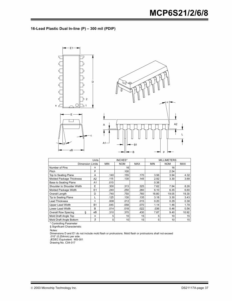
16-Lead Plastic Dual In-line (P) – 300 mil (PDIP)1510515105βMold Draft Angle Bottom1510515105αMold Draft Angle Top
10.929.407.87.430.370.310eBOverall Row Spacing §0.560.46.036.022.018.014BLower Lead Width1.781.461.14.070.058.045B1Upper Lead Width0.380.290.20.015.012.008cLead Thickness3.433.303.18.135.130.125LTip to Seating Plane
19.3019.0518.80.760.750.740DOverall Length6.606.356.10.260.250.240E1Molded Package Width8.267.947.62.325.313.300EShoulder to Shoulder Width
0.38.015A1Base to Seating Plane3.683.302.92.145.130.115A2Molded Package Thickness4.323.943.56.170.155.140ATop to Seating Plane
2.54.100pPitch1616nNumber of Pins
MAXNOMMINMAXNOMMINDimension LimitsMILLIMETERSINCHES*Units
2
1
D
n
E1
c
β
eB
E
α
p
L
A2
B
B1
A
A1
* Controlling Parameter
Notes:Dimensions D and E1 do not include mold flash or protrusions. Mold flash or protrusions shall not exceed .010” (0.254mm) per side.JEDEC Equivalent: MS-001Drawing No. C04-017
§ Significant Characteristic
2003 Microchip Technology Inc. DS21117A-page 37

MCP6S21/2/6/8
16-Lead Plastic Small Outline (SL) – Narrow 150 mil (SOIC)Foot Angle φ 0 4 8 0 4 8
1512015120βMold Draft Angle Bottom1512015120αMold Draft Angle Top
0.510.420.33.020.017.013BLead Width0.250.230.20.010.009.008cLead Thickness
1.270.840.41.050.033.016LFoot Length0.510.380.25.020.015.010hChamfer Distance
10.019.919.80.394.390.386DOverall Length3.993.903.81.157.154.150E1Molded Package Width6.206.025.79.244.237.228EOverall Width0.250.180.10.010.007.004A1Standoff §1.551.441.32.061.057.052A2Molded Package Thickness1.751.551.35.069.061.053AOverall Height
1.27.050pPitch1616nNumber of Pins
MAXNOMMINMAXNOMMINDimension LimitsMILLIMETERSINCHES*Units
α
A2
E1
1
2
L
h
nB
45°
E
p
D
φ
β
c
A1
A
* Controlling Parameter
Notes:Dimensions D and E1 do not include mold flash or protrusions. Mold flash or protrusions shall not exceed .010” (0.254mm) per side.JEDEC Equivalent: MS-012Drawing No. C04-108
§ Significant Characteristic
DS21117A-page 38 2003 Microchip Technology Inc.
MCP6S21/2/6/8
NOTES:2003 Microchip Technology Inc. DS21117A-page 39

MCP6S21/2/6/8
PRODUCT IDENTIFICATION SYSTEMTo order or obtain information, e.g., on pricing or delivery, refer to the factory or the listed sales office.Sales and SupportData SheetsProducts supported by a preliminary Data Sheet may have an errata sheet describing minor operational differences and recom-mended workarounds. To determine if an errata sheet exists for a particular device, please contact one of the following:
1. Your local Microchip sales office2. The Microchip Corporate Literature Center U.S. FAX: (480) 792-72773. The Microchip Worldwide Site (www.microchip.com)
Please specify which device, revision of silicon and Data Sheet (include Literature #) you are using.
New Customer Notification SystemRegister on our web site (www.microchip.com/cn) to receive the most current information on our products.
PART NO. -X /XX
PackageTemperatureRange
Device
Device: MCP6S21: One Channel PGA
MCP6S21T: One Channel PGA(Tape and Reel for SOIC and MSOP)
MCP6S22: Two Channel PGAMCP6S22T: Two Channel PGA
(Tape and Reel for SOIC and MSOP)MCP6S26: Six Channel PGAMCP6S26T: Six Channel PGA
(Tape and Reel for SOIC and TSSOP)MCP6S28: Eight Channel PGAMCP6S28T: Eight Channel PGA
(Tape and Reel for SOIC)
Temperature Range: I = -40°C to +85°C
Package: MS = Plastic Micro Small Outline (MSOP), 8-leadP = Plastic DIP (300 mil Body), 8, 14, and 16-leadSN = Plastic SOIC, (150 mil Body), 8-leadSL = Plastic SOIC (150 mil Body), 14, 16-leadST = Plastic TSSOP (4.4mm Body), 14-lead
Examples:a) MCP6S21-I/P: One Channel PGA,
PDIP package.b) MCP6S21-I/SN: One Channel PGA,
SOIC package.c) MCP6S21-I/MS: One Channel PGA,
MSOP package.d) MCP6S22-I/MS: Two Channel PGA,
MSOP package.e) MCP6S22T-I/MS: Tape and Reel,
Two Channel PGA, MSOP package.f) MCP6S26-I/P: Six Channel PGA,
PDIP package.g) MCP6S26-I/SN: Six Channel PGA,
SOIC package.h) MCP6S26T-I/ST: Tape and Reel,
Six Channel PGA, TSSOP package.i) MCP6S28T-I/SL: Tape and Reel,
Eight Channel PGA, SOIC package.
2002 Microchip Technology Inc. DS21117A-page 39
MCP6S21/2/6/8
NOTES:DS21117A-page 40 2002 Microchip Technology Inc.

Note the following details of the code protection feature on Microchip devices:• Microchip products meet the specification contained in their particular Microchip Data Sheet.
• Microchip believes that its family of products is one of the most secure families of its kind on the market today, when used in the intended manner and under normal conditions.
• There are dishonest and possibly illegal methods used to breach the code protection feature. All of these methods, to our knowledge, require using the Microchip products in a manner outside the operating specifications contained in Microchip's Data Sheets. Most likely, the person doing so is engaged in theft of intellectual property.
• Microchip is willing to work with the customer who is concerned about the integrity of their code.
• Neither Microchip nor any other semiconductor manufacturer can guarantee the security of their code. Code protection does not mean that we are guaranteeing the product as “unbreakable.”
Code protection is constantly evolving. We at Microchip are committed to continuously improving the code protection features of ourproducts. Attempts to break microchip’s code protection feature may be a violation of the Digital Millennium Copyright Act. If suchacts allow unauthorized access to your software or other copyrighted work, you may have a right to sue for relief under that Act.
Information contained in this publication regarding deviceapplications and the like is intended through suggestion onlyand may be superseded by updates. It is your responsibility toensure that your application meets with your specifications. Norepresentation or warranty is given and no liability is assumedby Microchip Technology Incorporated with respect to theaccuracy or use of such information, or infringement of patentsor other intellectual property rights arising from such use orotherwise. Use of Microchip’s products as critical components inlife support systems is not authorized except with expresswritten approval by Microchip. No licenses are conveyed,implicitly or otherwise, under any intellectual property rights.
2003 Microchip Technology Inc.
Trademarks
The Microchip name and logo, the Microchip logo, KEELOQ, MPLAB, PIC, PICmicro, PICSTART, PRO MATE and PowerSmart are registered trademarks of Microchip Technology Incorporated in the U.S.A. and other countries.
FilterLab, microID, MXDEV, MXLAB, PICMASTER, SEEVAL and The Embedded Control Solutions Company are registered trademarks of Microchip Technology Incorporated in the U.S.A.
Accuron, Application Maestro, dsPIC, dsPICDEM, dsPICDEM.net, ECONOMONITOR, FanSense, FlexROM, fuzzyLAB, In-Circuit Serial Programming, ICSP, ICEPIC, microPort, Migratable Memory, MPASM, MPLIB, MPLINK, MPSIM, PICC, PICkit, PICDEM, PICDEM.net, PowerCal, PowerInfo, PowerMate, PowerTool, rfLAB, rfPIC, Select Mode, SmartSensor, SmartShunt, SmartTel and Total Endurance are trademarks of Microchip Technology Incorporated in the U.S.A. and other countries.
Serialized Quick Turn Programming (SQTP) is a service mark ofMicrochip Technology Incorporated in the U.S.A.
All other trademarks mentioned herein are property of theirrespective companies.
© 2003, Microchip Technology Incorporated, Printed in theU.S.A., All Rights Reserved.
Printed on recycled paper.
DS21117A - page 41
Microchip received QS-9000 quality system certification for its worldwide headquarters, design and wafer fabrication facilities in Chandler and Tempe, Arizona in July 1999 and Mountain View, California in March 2002. The Company’s quality system processes and procedures are QS-9000 compliant for its PICmicro® 8-bit MCUs, KEELOQ® code hopping devices, Serial EEPROMs, microperipherals, non-volatile memory and analog products. In addition, Microchip’s quality system for the design and manufacture of development systems is ISO 9001 certified.

DS21117A-page 42 2003 Microchip Technology Inc.
MAMERICASCorporate Office2355 West Chandler Blvd.Chandler, AZ 85224-6199Tel: 480-792-7200 Fax: 480-792-7277Technical Support: 480-792-7627Web Address: http://www.microchip.comRocky Mountain2355 West Chandler Blvd.Chandler, AZ 85224-6199Tel: 480-792-7966 Fax: 480-792-4338Atlanta3780 Mansell Road, Suite 130Alpharetta, GA 30022Tel: 770-640-0034 Fax: 770-640-0307Boston2 Lan Drive, Suite 120Westford, MA 01886Tel: 978-692-3848 Fax: 978-692-3821Chicago333 Pierce Road, Suite 180Itasca, IL 60143Tel: 630-285-0071 Fax: 630-285-0075Dallas4570 Westgrove Drive, Suite 160Addison, TX 75001Tel: 972-818-7423 Fax: 972-818-2924DetroitTri-Atria Office Building 32255 Northwestern Highway, Suite 190Farmington Hills, MI 48334Tel: 248-538-2250 Fax: 248-538-2260Kokomo2767 S. Albright Road Kokomo, Indiana 46902Tel: 765-864-8360 Fax: 765-864-8387Los Angeles18201 Von Karman, Suite 1090Irvine, CA 92612Tel: 949-263-1888 Fax: 949-263-1338San JoseMicrochip Technology Inc.2107 North First Street, Suite 590San Jose, CA 95131Tel: 408-436-7950 Fax: 408-436-7955Toronto6285 Northam Drive, Suite 108Mississauga, Ontario L4V 1X5, CanadaTel: 905-673-0699 Fax: 905-673-6509
ASIA/PACIFICAustraliaMicrochip Technology Australia Pty LtdMarketing Support DivisionSuite 22, 41 Rawson StreetEpping 2121, NSWAustraliaTel: 61-2-9868-6733 Fax: 61-2-9868-6755China - BeijingMicrochip Technology Consulting (Shanghai)Co., Ltd., Beijing Liaison OfficeUnit 915Bei Hai Wan Tai Bldg.No. 6 Chaoyangmen Beidajie Beijing, 100027, No. ChinaTel: 86-10-85282100 Fax: 86-10-85282104China - ChengduMicrochip Technology Consulting (Shanghai)Co., Ltd., Chengdu Liaison OfficeRm. 2401-2402, 24th Floor, Ming Xing Financial TowerNo. 88 TIDU StreetChengdu 610016, ChinaTel: 86-28-86766200 Fax: 86-28-86766599China - FuzhouMicrochip Technology Consulting (Shanghai)Co., Ltd., Fuzhou Liaison OfficeUnit 28F, World Trade PlazaNo. 71 Wusi RoadFuzhou 350001, ChinaTel: 86-591-7503506 Fax: 86-591-7503521China - Hong Kong SARMicrochip Technology Hongkong Ltd.Unit 901-6, Tower 2, Metroplaza223 Hing Fong RoadKwai Fong, N.T., Hong KongTel: 852-2401-1200 Fax: 852-2401-3431China - ShanghaiMicrochip Technology Consulting (Shanghai)Co., Ltd.Room 701, Bldg. BFar East International PlazaNo. 317 Xian Xia RoadShanghai, 200051Tel: 86-21-6275-5700 Fax: 86-21-6275-5060China - ShenzhenMicrochip Technology Consulting (Shanghai)Co., Ltd., Shenzhen Liaison OfficeRm. 1812, 18/F, Building A, United PlazaNo. 5022 Binhe Road, Futian DistrictShenzhen 518033, ChinaTel: 86-755-82901380 Fax: 86-755-82966626China - QingdaoRm. B505A, Fullhope Plaza,No. 12 Hong Kong Central Rd.Qingdao 266071, ChinaTel: 86-532-5027355 Fax: 86-532-5027205IndiaMicrochip Technology Inc.India Liaison OfficeMarketing Support DivisionDivyasree Chambers1 Floor, Wing A (A3/A4)No. 11, O’Shaugnessey RoadBangalore, 560 025, IndiaTel: 91-80-2290061 Fax: 91-80-2290062
JapanMicrochip Technology Japan K.K.Benex S-1 6F3-18-20, ShinyokohamaKohoku-Ku, Yokohama-shiKanagawa, 222-0033, JapanTel: 81-45-471- 6166 Fax: 81-45-471-6122KoreaMicrochip Technology Korea168-1, Youngbo Bldg. 3 FloorSamsung-Dong, Kangnam-KuSeoul, Korea 135-882Tel: 82-2-554-7200 Fax: 82-2-558-5934SingaporeMicrochip Technology Singapore Pte Ltd.200 Middle Road#07-02 Prime CentreSingapore, 188980Tel: 65-6334-8870 Fax: 65-6334-8850TaiwanMicrochip Technology (Barbados) Inc., Taiwan Branch11F-3, No. 207Tung Hua North RoadTaipei, 105, TaiwanTel: 886-2-2717-7175 Fax: 886-2-2545-0139
EUROPEAustriaMicrochip Technology Austria GmbHDurisolstrasse 2A-4600 WelsAustriaTel: 43-7242-2244-399Fax: 43-7242-2244-393DenmarkMicrochip Technology Nordic ApSRegus Business CentreLautrup hoj 1-3Ballerup DK-2750 DenmarkTel: 45 4420 9895 Fax: 45 4420 9910FranceMicrochip Technology SARLParc d’Activite du Moulin de Massy43 Rue du Saule TrapuBatiment A - ler Etage91300 Massy, FranceTel: 33-1-69-53-63-20 Fax: 33-1-69-30-90-79GermanyMicrochip Technology GmbHSteinheilstrasse 10D-85737 Ismaning, GermanyTel: 49-089-627-144-100 Fax: 49-089-627-144-44ItalyMicrochip Technology SRLVia Quasimodo, 1220025 Legnano (MI)Milan, Italy Tel: 39-0331-742611 Fax: 39-0331-466781United KingdomMicrochip Ltd.505 Eskdale RoadWinnersh TriangleWokingham Berkshire, England RG41 5TUTel: 44 118 921 5869 Fax: 44-118 921-5820
02/12/03
WORLDWIDE SALES AND SERVICE