Embed Size (px)
Citation preview
Single Board ComputersProgrammer’s Reference Guide
(Part 2 of 2)VMESBCA2/PG1
Notice
While reasonable efforts have been made to assure the accuracy of this document, Motorola, Inc. assumes no liability resulting from any omissions in this document, or from the use of the information obtained therein. Motorola reserves the right to revise this document and to make changes from time to time in the content hereof without obligation of Motorola to notify any person of such revision or changes.
No part of this material may be reproduced or copied in any tangible medium, or stored in a retrieval system, or transmitted in any form, or by any means, radio, electronic, mechanical, photocopying, recording or facsimile, or otherwise, without the prior written permission of Motorola, Inc.
It is possible that this publication may contain reference to, or information about Motorola products (machines and programs), programming, or services that are not announced in your country. Such references or information must not be construed to mean that Motorola intends to announce such Motorola products, programming, or services in your country.
Restricted Rights Legend
If the documentation contained herein is supplied, directly or indirectly, to the U.S. Government, the following notice shall apply unless otherwise agreed to in writing by Motorola, Inc.
Use, duplication, or disclosure by the Government is subject to restrictions as set forth in subparagraph (c)(1)(ii) of the Rights in Technical Data and Computer Software clause at DFARS 252.227-7013.
Motorola, Inc.Computer Group
2900 South Diablo WayTempe, Arizona 85282
Preface
This manual provides board level information and detailed ASIC chip information including register bit descriptions for the MVME166, MVME167, MVME176, MVME177, and MVME187 Single Board Computers. The information in this manual applies to the single board computers listed in the following table:
Notes This document is bound in two parts. Part 1 (VMESBCA1/PGx)contains Chapters 1 through 4. Part 2 (VMESBCA2/PGx)contains Chapters 5 through 9.
This manual replaces the MVME166/167/187 Single BoardComputers ProgrammerÕs Reference Guide, MVME187PG/D3,and its supplement, MVME187PG/D3A1. They are obsolete.
This manual is intended for anyone who wants to program these boards in order to design OEM systems, supply additional capability to an existing compatible system, or work in a lab environment for experimental purposes.
A basic knowledge of computers and digital logic is assumed.
To use this manual, you should be familiar with the publications listed in Related Documentation below.
MVME166 Models
MVME167 Models
MVME176 Models
MVME177 Models
MVME187 Models
MVME166-011a MVME167-001a MVME176-001a MVME177-001a MVME187-001a
MVME166-012a MVME167-002a MVME176-002a MVME177-002a MVME187-002a
MVME166-013a MVME167-003a MVME176-003a MVME177-003a MVME187-003a
MVME166-014a MVME167-004a MVME176-004a MVME177-004a MVME187-004a
MVME166-015a MVME167-031a MVME176-005a MVME177-005a MVME187-023a
MVME166-016a MVME167-032a MVME176-006a MVME177-006a MVME187-024a
MVME167-033a MVME177-011a MVME187-031a
MVME167-034a MVME177-012a MVME187-032a
MVME167-035a MVME177-013a MVME187-033a
MVME167-036a MVME177-014a MVME187-034a
MVME177-015a MVME187-035a
MVME177-016a MVME187-036a
The letter “a” in the model number indicates the major revision level.
Related DocumentationThe following publications are applicable to the Single Board Computers and may provide additional helpful information. If not shipped with this product, they may be purchased by contacting your local Motorola sales ofÞce. Non-Motorola documents may be obtained from the sources listed.
Document Title MotorolaPublication Number
MVME166 Single Board Computer User's Manual MVME166/D
MVME167 Single Board Computer User's Manual MVME167/D
MVME176 Single Board Computer Installation and Use Manual VME176A/IH
MVME177 Single Board Computer Installation and Use Manual VME177A/IH
MVME167Bug Debugging Package User's Manual MVME167BUG/D
MVME177Bug Diagnostics User's Manual V177DIAA/UM
Debugging Package for Motorola 68K CISC CPUs User's Manual (Parts 1 and 2)
68KBUG1/D and 68KBUG2/D
MVME187 RISC Single Board Computer User's Manual MVME187/D
MVME187Bug Debugging Package User's Manual MVME187BUG/D
Debugging Package for Motorola 88K RISC CPUs User's Manual
88KBUG1/D and 88KBUG2/D
Single Board Computers SCSI Software User's Manual SBCSCSI/D
MVME712-06/07/09 I/O Distribution Board Set User's Manual MVME712IO/D
MVME712-10 Transition Module User's Manual MVME712-10/D
MVME712M Transition Module and P2 Adapter Board User's Manual
MVME712M/D
MVME712-12, MVME712-13, MVME712A, MVME712AM, and MVME712B Transition Modules and LCP2 Adapter Board User's Manual
MVME712A/D
Note Although not shown in the above list, each Motorola ComputerGroup manual publication number is suffixed with characterswhich represent the revision level of the document, such as Ò/xx2Ó (the second revision of a manual); a supplement bears thesame number as a manual but has a suffix such as Ò/xx2A1Ó (thefirst supplement to the second edition of the manual).
The following publications are available from the sources indicated:
Versatile Backplane Bus: VMEbus, ANSI/IEEE Std 1014-1987, The Institute of Electrical and Electronics Engineers, Inc., 345 East 47th Street, New York, NY 10017 (VMEbus SpeciÞcation). (This is also Microprocessor System Bus for 1 to 4 Byte Data, IEC 821 BUS, Bureau Central de la Commission Electrotechnique Internationale; 3, rue de Varemb�, Geneva, Switzerland.)
Z85230 Serial Communications Controller Data Sheet, order number DC-8293-02, Zilog Inc., 210 East Hacienda Drive, Campbell, CA 95008-6600.
IEEE Standard for Multiplexed High-Performance Bus Structure: VSB, ANSI/IEEE Std 1096-1988, The Institute of Electrical and Electronics Engineers, Inc., 345 East 47th Street, New York, NY 10017 (VSB SpeciÞcation). (This is also Parallel Sub-system Bus of the IEC 821 VMEbus, IEC 822 VSB, Bureau Central de la Commission Electrotechnique Internationale; 3, rue de Varemb�, Geneva, Switzerland.)
ANSI Small Computer System Interface-2 (SCSI-2), Draft Document X3.131-198X, Revision 10c; Global Engineering Documents, 15 Inverness Way East, Englewood, CO 80112-5704.
CL-CD2400/2401 Four-Channel Multi-Protocol Communications Controller Data Sheet, order number 542400-003; Cirrus Logic, Inc., 3100 West Warren Ave., Fremont, CA 94538.
MC88100 RISC Microprocessor User's Manual MC88100UM
MC88200 Cache/Memory Management Unit (CMMU) User's Manual
MC88200UM
M68040 Microprocessors User's Manual M68040UM
M68060 Microprocessors User's Manual M68060UM
M68000 Family Reference Manual M68000FR
Document Title MotorolaPublication Number
82596CA Local Area Network Coprocessor Data Sheet, order number 290218; and 82596 User's Manual, order number 296853; Intel Corporation, Literature Sales, P.O. Box 58130, Santa Clara, CA 95052-8130.
DS1643 Nonvolatile Timekeeping RAM, Dallas Semiconductor Data Manual, 4401 South Beltwood Parkway, Dallas, Texas 75244-3292.
NCR 53C710 SCSI I/O Processor Data Manual, order number NCR53C710DM, and NCR 53C710 SCSI I/O Processor ProgrammerÕs Guide, order number NCR53C710PG; NCR Corporation, Microelectronics Products Division, 1635 Aeroplaza Dr., Colorado Springs, CO 80916.
MK48T08(B)/MK48T18(B) TimekeeperTM and 8Kx8 ZeropowerTM RAM data sheet in Static RAMs Databook, order number DBSRAM71; SGS-THOMSON Microelectronics; North & South American Marketing Headquarters, 1000 East Bell Road, Phoenix, AZ 85022-2699.
i28F008 Flash Memory Data Sheet, order number 290435, i28F020 Flash Memory Data Sheet, order number 290245, i28F008SA Software Drivers Application Note, order number 292095, and i28F008SA Automation and Algorithms Application Note, order number 292099; Intel Literature Sales, P.O. Box 7641, Mt. Prospect, IL 60056-7641.
MC68230 Parallel Interface Timer (PI/T) Data Sheet, order number MC68230/D, Motorola Semiconductor Products, Inc., LDC, Broadway Bldg. BB100, P.O. Box 20924, Phoenix, AZ 85036-0924.
Manual Terminology
Throughout this manual, a convention is used which precedes data and address parameters by a character identifying the numeric format as follows:
For example, Ò12Ó is the decimal number twelve, and Ò$12Ó is the decimal number eighteen.
Unless otherwise speciÞed, all address references are in hexadecimal.
An asterisk (*) following the signal name for signals which are level signiÞcant denotes that the signal is true or valid when the signal is low.
$
%
&
dollar
percent
ampersand
specifies a hexadecimal character
specifies a binary number
specifies a decimal number
An asterisk (*) following the signal name for signals which are edge signiÞcant denotes that the actions initiated by that signal occur on high to low transition.
In this manual, assertion and negation are used to specify forcing a signal to a particular state. In particular, assertion and assert refer to a signal that is active or true; negation and negate indicate a signal that is inactive or false. These terms are used independently of the voltage level (high or low) that they represent.
Data and address sizes are deÞned as follows: ❏ A byte is eight bits, numbered 0 through 7, with bit 0 being the least significant.
❏ A two-byte is 16 bits, numbered 0 through 15, with bit 0 being the least significant. For the MVME166, MVME167, MVME176, MVME177, and other CISC boards, this is called a word. For the MVME187 and other RISC boards, this is called a half-word.
❏ A four-byte is 32 bits, numbered 0 through 31, with bit 0 being the least significant. For the MVME166, MVME167, MVME176, MVME177, and other CISC boards, this is called a longword. For the MVME187 and other RISC boards, this is called a word.
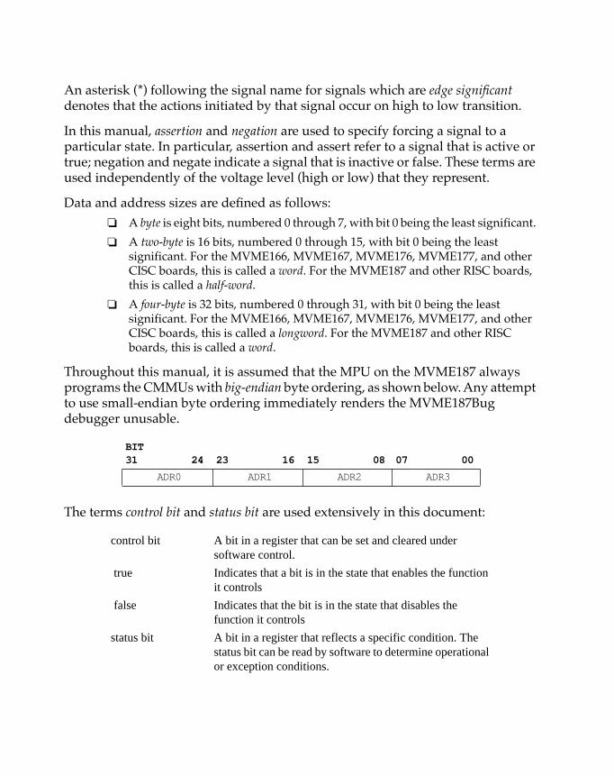
Throughout this manual, it is assumed that the MPU on the MVME187 always programs the CMMUs with big-endian byte ordering, as shown below. Any attempt to use small-endian byte ordering immediately renders the MVME187Bug debugger unusable.
The terms control bit and status bit are used extensively in this document:
BIT31 24 23 16 15 08 07 00
ADR0 ADR1 ADR2 ADR3
control bit A bit in a register that can be set and cleared under software control.
true Indicates that a bit is in the state that enables the function it controls
false Indicates that the bit is in the state that disables the function it controls
status bit A bit in a register that reflects a specific condition. The status bit can be read by software to determine operational or exception conditions.
In all tables, the terms 0 and 1 are used to describe the actual value that should be written to the bit, or the value that it yields when read.
The computer programs stored in the Read Only Memory of this device contain material copyrighted by Motorola Inc., Þrst published 1990, and may be used only under a license such as the License for Computer Programs (Article 14) contained in Motorola's Terms and Conditions of Sale, Rev. 1/79.
!WARNING
This equipment generates, uses, and can radiate electro-magnetic energy. It may cause or be susceptible to electro-magnetic interference (EMI) if not installed and used in acabinet with adequate EMI protection.
Motorola¨ and the Motorola symbol are registered trademarks of Motorola, Inc.
Delta Series, SYSTEM V/68, SYSTEM V/88, VMEmodule, and VMEsystem are trademarks of Motorola, Inc.
Timekeeper and Zeropower are trademarks of SGS-THOMSON Microelectronics.
All other products mentioned in this document are trademarks or registered trademarks of their respective holders.
© Copyright Motorola 1995, 1996
All Rights Reserved
Printed in the United States of America
June 1996
Contents
Chapter 1 Programming Issues
Introduction ..........................................................................................................1-1Programming Interfaces......................................................................................1-1
MC68040 MPU ...............................................................................................1-2MC68060 MPU ...............................................................................................1-2M88000 MPU ..................................................................................................1-2Data Bus Structure.........................................................................................1-2EPROMs on the MVME167/176/177/187.................................................1-3
MVME167 and MVME187 .................................................................... 1-3MVME176/177 ....................................................................................... 1-3
Flash Memory on the MVME176/177 ........................................................1-4Flash Memory and Download EPROM on the MVME166......................1-5SRAM ..............................................................................................................1-6Onboard DRAM.............................................................................................1-7Battery Backed Up RAM and Clock............................................................1-7VMEbus Interface ..........................................................................................1-8VME Subsystem Bus (VSB) Interface..........................................................1-8I/O Interfaces .................................................................................................1-8
Serial Port Interface................................................................................ 1-8MC68230 Parallel Interface/Timer (MVME166/176 Only) ........... 1-10Parallel (Printer) Interface................................................................... 1-12Ethernet Interface ................................................................................. 1-12SCSI Interface........................................................................................ 1-13
Local Resources............................................................................................1-14Programmable Tick Timers ................................................................ 1-14Watchdog Timer................................................................................... 1-14Software-Programmable Hardware Interrupts ............................... 1-14Local Bus Time-out .............................................................................. 1-14
Interrupt Handling.............................................................................................1-15Interrupt Programming Examples ............................................................1-16
M68000 VMEchip2 Tick Timer 1 Periodic Interrupt Example ...... 1-17MVME187 Interrupt Handling........................................................... 1-19
Cache Coherency................................................................................................1-23Cache Coherency, MVME166/167 ............................................................1-23
ix
Cache Coherency, MVME176/177 ............................................................ 1-23Cache Coherency, MVME187..................................................................... 1-24
Using Bus Timers ............................................................................................... 1-24Indivisible Cycles ............................................................................................... 1-26No Supervisor Stack Pointer on MC68060 ..................................................... 1-27Sources of Local BERR* ..................................................................................... 1-27
Local Bus Time-out...................................................................................... 1-28VMEbus Access Time-out........................................................................... 1-28VMEbus BERR*............................................................................................ 1-28Local DRAM Parity Error........................................................................... 1-28VMEchip2 ..................................................................................................... 1-28VSBchip2 BERR* .......................................................................................... 1-29Bus Error Processing ................................................................................... 1-29
Error Conditions................................................................................................. 1-29MPU Parity Error......................................................................................... 1-30MPU Offboard Error ................................................................................... 1-30MPU TEA - Cause UnidentiÞed ................................................................ 1-30MPU Local Bus Time-out ........................................................................... 1-31DMAC VMEbus Error ................................................................................ 1-31DMAC Parity Error ..................................................................................... 1-31DMAC Offboard Error................................................................................ 1-32DMAC LTO Error ........................................................................................ 1-32DMAC TEA - Cause UnidentiÞed............................................................. 1-32SCC Retry Error ........................................................................................... 1-34SCC Parity Error .......................................................................................... 1-34SCC Offboard Error..................................................................................... 1-34SCC LTO Error ............................................................................................. 1-36LAN Parity Error ......................................................................................... 1-36LAN Offboard Error.................................................................................... 1-36LAN LTO Error ............................................................................................ 1-37SCSI Parity Error.......................................................................................... 1-37SCSI Offboard Error .................................................................................... 1-37SCSI LTO Error............................................................................................. 1-38
Chapter 2 Hardware Configuration
Introduction .......................................................................................................... 2-1SCSI Termination ................................................................................................. 2-1Connectors ............................................................................................................ 2-2
x
Fuses.......................................................................................................................2-2MVME166 Fuses ............................................................................................2-3MVME176 Polyswitches ...............................................................................2-3MVME167/177/187 Fuses ...........................................................................2-3
ConÞguration Jumpers........................................................................................2-4ConÞguration Jumpers, MVME166 ............................................................2-5ConÞguration Jumpers, MVME167 ............................................................2-8ConÞguration Jumpers, MVME177 ..........................................................2-12ConÞguration Jumpers, MVME187 ..........................................................2-16ConÞguration Jumpers, MVME176 ..........................................................2-20
Chapter 3 Memory Maps
Introduction ..........................................................................................................3-1VMEbus Memory Map........................................................................................3-1VSB Memory Map................................................................................................3-2Local Bus Memory Map ......................................................................................3-2
Normal Address Range.................................................................................3-2Detailed I/O Memory Maps ........................................................................3-3
Chapter 4 VMEchip2
Introduction ..........................................................................................................4-1Summary of Features...........................................................................................4-1Functional Blocks .................................................................................................4-4
Local Bus to VMEbus Interface....................................................................4-4Local Bus to VMEbus Requester .......................................................... 4-8
VMEbus to Local Bus Interface....................................................................4-9Local Bus to VMEbus DMA Controller .................................................... 4-11
DMAC VMEbus Requester................................................................ 4-13Tick and Watchdog Timers .........................................................................4-14
Prescaler................................................................................................. 4-14Tick Timer ............................................................................................. 4-14Watchdog Timer................................................................................... 4-15
VMEbus Interrupter ....................................................................................4-16VMEbus System Controller........................................................................4-17
Arbiter.................................................................................................... 4-17IACK Daisy-Chain Driver................................................................... 4-17Bus Timer .............................................................................................. 4-17
xi
Reset Driver 4-18Local Bus Interrupter and Interrupt Handler ......................................... 4-18Global Control and Status Registers......................................................... 4-20VMEboard Functions .................................................................................. 4-20
LCSR Programming Model .............................................................................. 4-21Programming the VMEbus Slave Map Decoders ................................... 4-26
VMEbus Slave Ending Address Register 1 ...................................... 4-29VMEbus Slave Starting Address Register 1 ..................................... 4-29VMEbus Slave Ending Address Register 2 ...................................... 4-29VMEbus Slave Starting Address Register 2 ..................................... 4-30VMEbus Slave Address Translation Address Offset Register 1 ... 4-30VMEbus Slave Address Translation Select Register 1.................... 4-31VMEbus Slave Address Translation Address Offset Register 2 ... 4-32VMEbus Slave Address Translation Select Register 2 .................... 4-32VMEbus Slave Write Post and Snoop Control Register 2.............. 4-33VMEbus Slave Address Modifier Select Register 2 ........................ 4-34VMEbus Slave Write Post and Snoop Control Register 1.............. 4-35VMEbus Slave Address Modifier Select Register 1 ........................ 4-36
Programming the Local Bus to VMEbus Map Decoders....................... 4-37Local Bus Slave (VMEbus Master) Ending Address Register 1 .... 4-40Local Bus Slave (VMEbus Master) Starting Address Register 1 ... 4-40Local Bus Slave (VMEbus Master) Ending Address Register 2 .... 4-40Local Bus Slave (VMEbus Master) Starting Address Register 2 ... 4-41Local Bus Slave (VMEbus Master) Ending Address Register 3 .... 4-41Local Bus Slave (VMEbus Master) Starting Address Register 3 ... 4-41Local Bus Slave (VMEbus Master) Ending Address Register 4 .... 4-42Local Bus Slave (VMEbus Master) Starting Address Register 4 ... 4-42Local Bus Slave (VMEbus Master) Address Translation Address Register 4 .............................................................................. 4-42Local Bus Slave (VMEbus Master) Address Translation Select Register 4 ................................................................................... 4-43Local Bus Slave (VMEbus Master) Attribute Register 4................. 4-43Local Bus Slave (VMEbus Master) Attribute Register 3................. 4-44Local Bus Slave (VMEbus Master) Attribute Register 2................. 4-44Local Bus Slave (VMEbus Master) Attribute Register 1................. 4-45VMEbus Slave GCSR Group Address Register ............................... 4-46VMEbus Slave GCSR Board Address Register ................................ 4-46Local Bus To VMEbus Enable Control Register .............................. 4-47
xii
Local Bus To VMEbus I/O Control Register ................................... 4-48ROM Control Register ......................................................................... 4-49
Programming the VMEchip2 DMA Controller .......................................4-52DMAC Registers................................................................................... 4-53PROM Decoder, SRAM and DMA Control Register ...................... 4-54Local Bus To VMEbus Requester Control Register......................... 4-56DMAC Control Register 1 (bits 0-7) .................................................. 4-57DMAC Control Register 2 (bits 8-15) ................................................ 4-59DMAC Control Register 2 (bits 0-7) .................................................. 4-60DMAC Local Bus Address Counter .................................................. 4-61DMAC VMEbus Address Counter.................................................... 4-62DMAC Byte Counter ........................................................................... 4-62Table Address Counter ....................................................................... 4-63VMEbus Interrupter Control Register .............................................. 4-63VMEbus Interrupter Vector Register ................................................ 4-64MPU Status and DMA Interrupt Count Register ............................ 4-65DMAC Status Register ........................................................................ 4-66
Programming the Tick and Watchdog Timers.........................................4-67VMEbus Arbiter Time-out Control Register .................................... 4-67DMAC Timers and VMEbus Global Time-out Control Register ................................................................................................. 4-68 VME Access, Local Bus and Watchdog Time-out Control Register ................................................................................................. 4-69Prescaler Control Register................................................................... 4-70Tick Timer 1 Compare Register ......................................................... 4-71Tick Timer 1 Counter........................................................................... 4-71Tick Timer 2 Compare Register ......................................................... 4-72Tick Timer 2 Counter........................................................................... 4-72Board Control Register ........................................................................ 4-73Watchdog Timer Control Register..................................................... 4-74Tick Timer 2 Control Register ............................................................ 4-75Tick Timer 1 Control Register ............................................................ 4-76Prescaler Counter ................................................................................. 4-76
Programming the Local Bus Interrupter ..................................................4-77Local Bus Interrupter Status Register (bits 24-31) ........................... 4-80Local Bus Interrupter Status Register (bits 16-23) ........................... 4-81Local Bus Interrupter Status Register (bits 8-15) ............................. 4-82Local Bus Interrupter Status Register (bits 0-7) ............................... 4-83
xiii
Local Bus Interrupter Enable Register (bits 24-31).......................... 4-84 Local Bus Interrupter Enable Register (bits 16-23)......................... 4-85Local Bus Interrupter Enable Register (bits 8-15)............................ 4-86Local Bus Interrupter Enable Register (bits 0-7).............................. 4-87Software Interrupt Set Register (bits 8-15) ....................................... 4-88Interrupt Clear Register (bits 24-31).................................................. 4-88Interrupt Clear Register (bits 16-23).................................................. 4-89Interrupt Clear Register (bits 8-15).................................................... 4-90Interrupt Level Register 1 (bits 24-31)............................................... 4-90Interrupt Level Register 1 (bits 16-23)............................................... 4-91Interrupt Level Register 1 (bits 8-15)................................................. 4-91Interrupt Level Register 1 (bits 0-7)................................................... 4-92Interrupt Level Register 2 (bits 24-31)............................................... 4-92Interrupt Level Register 2 (bits 16-23)............................................... 4-93Interrupt Level Register 2 (bits 8-15)................................................. 4-93Interrupt Level Register 2 (bits 0-7)................................................... 4-94Interrupt Level Register 3 (bits 24-31)............................................... 4-94Interrupt Level Register 3 (bits 16-23)............................................... 4-95Interrupt Level Register 3 (bits 8-15)................................................. 4-95Interrupt Level Register 3 (bits 0-7)................................................... 4-96Interrupt Level Register 4 (bits 24-31)............................................... 4-96Interrupt Level Register 4 (bits 16-23)............................................... 4-97Interrupt Level Register 4 (bits 8-15)................................................. 4-97Interrupt Level Register 4 (bits 0-7)................................................... 4-98Vector Base Register ............................................................................ 4-98I/O Control Register 1 ........................................................................ 4-99I/O Control Register 2 ...................................................................... 4-100I/O Control Register 3 ...................................................................... 4-104Miscellaneous Control Register ....................................................... 4-105
GCSR Programming Model............................................................................ 4-107Programming the GCSR........................................................................... 4-109
VMEchip2 Revision Register............................................................ 4-111VMEchip2 ID Register....................................................................... 4-111VMEchip2 LM/SIG Register ............................................................ 4-111VMEchip2 Board Status/Control Register..................................... 4-113General Purpose Register 0 .............................................................. 4-114General Purpose Register 1 .............................................................. 4-114General Purpose Register 2 .............................................................. 4-115
xiv
General Purpose Register 3............................................................... 4-115General Purpose Register 4............................................................... 4-116General Purpose Register 5............................................................... 4-116
Chapter 5 VSBchip2
Introduction ..........................................................................................................5-1Summary of Features...........................................................................................5-1Functional Description ........................................................................................5-3
VSB to Local Bus Interface............................................................................5-5VSB Slave Interface ................................................................................ 5-5Programmable Map Decoders ............................................................. 5-5Write Post Buffer .................................................................................... 5-6Local Bus Master Interface.................................................................... 5-6VSB Block Transfer to a Local Bus Burst ............................................ 5-8
Local Bus to VSB Interface............................................................................5-8Local Bus Slave Interface....................................................................... 5-9Programmable Map Decoders ............................................................. 5-9Bounce Mode .......................................................................................... 5-9Write Post Buffer .................................................................................. 5-10VSB Master Interface ........................................................................... 5-11VSB Dynamic Bus Sizing..................................................................... 5-11VSB Timers............................................................................................ 5-11VSB Block Transfers............................................................................. 5-12
VSB Requester and VSB Serial Arbiter .....................................................5-13VSB Geographical Addressing........................................................... 5-13VSB Requesters..................................................................................... 5-14VSB Serial Arbiter ................................................................................ 5-16Arbitration Timer ................................................................................. 5-16
VSB Interrupter ............................................................................................5-16VSB Interrupt Handler................................................................................5-18Local Bus Interrupter ..................................................................................5-18Control and Status Registers......................................................................5-19
Local Control and Status Registers Programming Model............................5-20Chip Control/Status Register ....................................................................5-23Local Interrupt Vector Base Register.........................................................5-25Local Interrupt Status Register ..................................................................5-26Local Interrupt Enable Register .................................................................5-27Local Interrupt Level Register ...................................................................5-29
xv
Reserved Register ........................................................................................ 5-30VSB Requester Control/Status Register................................................... 5-31Timer Control Register ............................................................................... 5-33Timer Clock Prescaler Register.................................................................. 5-34Local Bus Slave 1 Address Range Register .............................................. 5-35Local Bus Slave 1 Address Offset Register............................................... 5-36Local Bus Slave 1 Attribute Register......................................................... 5-36Local Bus Slave 2 Address Range Register .............................................. 5-38Local Bus Slave 2 Address Offset Register............................................... 5-39Local Bus Slave 2 Attribute Register......................................................... 5-39Local Bus Slave 3 Address Range Register .............................................. 5-41Local Bus Slave 3 Address Offset Register............................................... 5-42Local Bus Slave 3 Attribute Register......................................................... 5-42Local Bus Slave 4 Address Range Register .............................................. 5-44Local Bus Slave 4 Address Offset Register............................................... 5-45Local Bus Slave 4 Attribute Register......................................................... 5-45Reserved Registers ...................................................................................... 5-46Local Error Address Register..................................................................... 5-47Prescaler Current Count Register ............................................................. 5-47Prescaler Test Register ................................................................................ 5-48
Board Control and Status Registers Programming Model .......................... 5-50EVSB Attention Register............................................................................. 5-52EVSB Test and Set (TAS) Register ............................................................. 5-54General Purpose Register 1........................................................................ 5-55General Purpose Register 2........................................................................ 5-55VSB Error Status Register........................................................................... 5-56VSB Interrupt Control Register ................................................................. 5-57VSB Interrupt Vector Register.................................................................... 5-58VSB Interrupt Enable Register................................................................... 5-59VSB Interrupt Status Register .................................................................... 5-60VSB Slave 1 Address Range Register........................................................ 5-61VSB Slave 1 Address Offset Register ........................................................ 5-61VSB Slave 1 Attribute Register .................................................................. 5-62VSB Slave 2 Address Range Register........................................................ 5-65VSB Slave 2 Address Offset Register ........................................................ 5-65VSB Slave 2 Attribute Register .................................................................. 5-66Reserved Register ........................................................................................ 5-69VSB Error Address Register ....................................................................... 5-69
xvi
Chapter 6 PCCchip2
Introduction ..........................................................................................................6-1Summary of Major Features.........................................................................6-1
Functional Description ........................................................................................6-2General Description.......................................................................................6-2BBRAM Interface ...........................................................................................6-3Download ROM Interface (MVME166 Only)............................................6-382596CA LAN Controller Interface.............................................................6-4
MPU Port and MPU Channel Attention............................................. 6-4MC68040-Bus Master Support for 82596CA ...................................... 6-5LANC Bus Error ..................................................................................... 6-5LANC Interrupt...................................................................................... 6-6
53C710 SCSI Controller Interface ................................................................6-7Memory Controller MEMC040 Interface ...................................................6-7Parallel Port Interface....................................................................................6-7General Purpose I/O Pin..............................................................................6-8CD2401 SCC Interface ...................................................................................6-8Interrupt Prioritizer (MVME187) ..............................................................6-10Tick Timer ..................................................................................................... 6-11
Overall Memory Map ........................................................................................6-12Programming Model..........................................................................................6-13
Chip ID Register...........................................................................................6-16Chip Revision Register................................................................................6-16General Control Register ............................................................................6-17Vector Base Register ....................................................................................6-18Programming the Tick Timers ...................................................................6-20
Tick Timer 1 Compare Register ......................................................... 6-20Tick Timer 1 Counter........................................................................... 6-21Tick Timer 2 Compare Register ......................................................... 6-21Tick Timer 2 Counter........................................................................... 6-22Prescaler Count Register ..................................................................... 6-22Prescaler Clock Adjust Register ......................................................... 6-22Tick Timer 2 Control Register ............................................................ 6-24Tick Timer 1 Control Register ............................................................ 6-25General Purpose Input Interrupt Control Register ......................... 6-26General Purpose Input/Output Pin Control Register.................... 6-27Tick Timer 2 Interrupt Control Register ........................................... 6-27Tick Timer 1 Interrupt Control Register ........................................... 6-28
xvii
SCC Error Status Register and Interrupt Control Registers .................. 6-29SCC Error Status Register ................................................................... 6-29SCC Modem Interrupt Control Register .......................................... 6-30SCC Transmit Interrupt Control Register ........................................ 6-31SCC Receive Interrupt Control Register........................................... 6-32Modem PIACK Register ..................................................................... 6-33Transmit PIACK Register ................................................................... 6-34Receive PIACK Register...................................................................... 6-35
LANC Error Status and Interrupt Control Registers ............................. 6-36LANC Error Status Register ............................................................... 6-3682596CA LANC Interrupt Control Register .................................... 6-37LANC Bus Error Interrupt Control Register ................................... 6-38
Programming the SCSI Error Status and Interrupt Registers ............... 6-39SCSI Error Status Register .................................................................. 6-39SCSI Interrupt Control Register......................................................... 6-40
Programming the Printer Port................................................................... 6-41Printer ACK Interrupt Control Register ........................................... 6-41Printer FAULT Interrupt Control Register ...................................... 6-42Printer SEL Interrupt Control Register............................................. 6-43Printer PE Interrupt Control Register ............................................... 6-44Printer BUSY Interrupt Control Register ......................................... 6-45Printer Input Status Register .............................................................. 6-46Printer Port Control Register.............................................................. 6-47Chip Speed Register ............................................................................ 6-48Printer Data Register ........................................................................... 6-49Interrupt Priority Level Register ....................................................... 6-50Interrupt Mask Level Register ........................................................... 6-51
Chapter 7 MEMC040
Introduction .......................................................................................................... 7-1Summary of Features........................................................................................... 7-1Functional Description........................................................................................ 7-2
General Description ...................................................................................... 7-2Performance ................................................................................................... 7-2Status and Control Registers........................................................................ 7-5
Register 1 - Chip ID Register................................................................ 7-7Register 2 - Chip Revision Register ..................................................... 7-7Register 3 - Memory Configuration Register..................................... 7-8
xviii
Register 4 - Alternate Status Register................................................ 7-10Register 5 - Alternate Control Register ............................................. 7-10Register 6 - Base Address Register .................................................... 7-10Register 7 - RAM Control Register .................................................... 7-11Register 8 - Bus Clock Register........................................................... 7-13
Chapter 8 MCECC
Introduction ..........................................................................................................8-1Summary of Features...........................................................................................8-1Functional Description ........................................................................................8-2
General Description.......................................................................................8-2Performance....................................................................................................8-2Cache Coherency ...........................................................................................8-3ECC ..................................................................................................................8-4
Cycle Types ............................................................................................. 8-4Error Reporting ...................................................................................... 8-5Single Bit Error (Cycle Type = Burst Read or Non-Burst Read)...... 8-5Double Bit Error (Cycle Type = Burst Read or Non-Burst Read) ... 8-5Triple (or Greater) Bit Error (Cycle Type = Burst Read or Non-Burst Read).................................................................................... 8-6Cycle Type = Burst Write...................................................................... 8-6Single Bit Error (Cycle Type = Non-Burst Write).............................. 8-6Double Bit Error (Cycle Type = Non-Burst Write)............................ 8-6Triple (or Greater) Bit Error (Cycle Type = Non-Burst Write) ........ 8-6Single Bit Error (Cycle Type = Scrub) ................................................. 8-7Double Bit Error (Cycle Type = Scrub) ............................................... 8-7Triple (or Greater) Bit Error (Cycle Type = Scrub)............................ 8-7
Error Logging .................................................................................................8-7Scrub ................................................................................................................8-7Refresh.............................................................................................................8-8Arbitration ......................................................................................................8-8Chip Defaults..................................................................................................8-9
Programming Model............................................................................................8-9Chip ID Register...........................................................................................8-14Chip Revision Register................................................................................8-14Memory ConÞguration Register ...............................................................8-15Dummy Register 0.......................................................................................8-16Dummy Register 1.......................................................................................8-17
xix
Base Address Register................................................................................. 8-17DRAM Control Register ............................................................................. 8-18BCLK Frequency Register .......................................................................... 8-20Data Control Register.................................................................................. 8-21Scrub Control Register................................................................................ 8-23Scrub Period Register Bits 15-8.................................................................. 8-24Scrub Period Register Bits 7-0.................................................................... 8-24Chip Prescaler Counter............................................................................... 8-25Scrub Time On/Time Off Register ............................................................ 8-25Scrub Prescaler Counter (Bits 21-16)......................................................... 8-27Scrub Prescaler Counter (Bits 15-8)........................................................... 8-27Scrub Prescaler Counter (Bits 7-0)............................................................. 8-27Scrub Timer Counter (Bits 15-8) ................................................................ 8-28Scrub Timer Counter (Bits 7-0) .................................................................. 8-28Scrub Address Counter (Bits 26-24) .......................................................... 8-28Scrub Address Counter (Bits 23-16) .......................................................... 8-29Scrub Address Counter (Bits 15-8) ............................................................ 8-29Scrub Address Counter (Bits 7-4) .............................................................. 8-30Error Logger Register.................................................................................. 8-30Error Address (Bits 31-24) .......................................................................... 8-31Error Address (Bits 23-16) .......................................................................... 8-32Error Address Bits (15-8) ............................................................................ 8-32Error Address Bits (7-4) .............................................................................. 8-32Error Syndrome Register............................................................................ 8-33Defaults Register 1 ...................................................................................... 8-33Defaults Register 2 ...................................................................................... 8-35Initialization ................................................................................................. 8-36
Syndrome Decode.............................................................................................. 8-38
Chapter 9 Printer and Serial Port Connections
Introduction .......................................................................................................... 9-1Connection Diagrams.......................................................................................... 9-1
xx
Figures
Figure 1-1. MVME176/177 Flash and EPROM Memory Mapping Schemes ............................................................................................................1-5Figure 1-2. MVME187 Interrupt Handling Protocol ....................................1-22Figure 4-1. VMEchip2 Block Diagram..............................................................4-5Figure 5-1. VSBchip2 Block Diagram................................................................5-4Figure 6-1. PCCchip2 Block Diagram...............................................................6-2Figure 7-1. Block Diagram for Memory Using MEMC040 ............................7-4Figure 9-1. MVME167/177/187 Printer Port with MVME712A ..................9-3Figure 9-2. MVME167/177/187 Printer Port with MVME712M..................9-4Figure 9-3. MVME167/177/187 Serial Port 1 ConÞgured as DCE...............9-5Figure 9-4. MVME167/177/187 Serial Port 2 ConÞgured as DCE...............9-6Figure 9-5. MVME167/177/187 Serial Port 3 ConÞgured as DCE...............9-7Figure 9-6. MVME167/177/187 Serial Port 4 ConÞgured as DCE...............9-8Figure 9-7. MVME167/177/187 Serial Port 1 ConÞgured as DTE ...............9-9Figure 9-8. MVME167/177/187 Serial Port 2 ConÞgured as DTE .............9-10Figure 9-9. MVME167/177/187 Serial Port 3 ConÞgured as DTE ............. 9-11Figure 9-10. MVME167/177/187 Serial Port 4 ConÞgured as DTE............9-12Figure 9-11. MVME167/177/187 Serial Port 1 with MVME712A...............9-13Figure 9-12. MVME167/177/187 Serial Port 2 with MVME712A...............9-14Figure 9-13. MVME167/177/187 Serial Port 3 with MVME712A...............9-15Figure 9-14. MVME167/177/187 Serial Port 4 with MVME712A...............9-16Figure 9-15. MVME166/176 Serial Ports with MVME712-10 (Sheet 1 of 4) .......................................................................................................9-17Figure 9-15. MVME166/176 Serial Ports with MVME712-10 (Sheet 2 of 4) .......................................................................................................9-18Figure 9-15. MVME166/176 Serial Ports with MVME712-10 (Sheet 3 of 4) ........................................................................................................9-19Figure 9-15. MVME166/176 Serial Ports with MVME712-10 (Sheet 4 of 4) .......................................................................................................9-20
xxi
Figure 9-16. MVME166/176 Serial Ports with MVME712-06 (Sheet 1 of 3)....................................................................................................... 9-21Figure 9-16. MVME166/176 Serial Ports withMVME712-06 (Sheet 2 of 3)........................................................................................................ 9-22Figure 9-16. MVME166/176 Serial Ports with MVME712-06 (Sheet 3 of 3)....................................................................................................... 9-23
xxii
Tables
Table 1-1. Single-Cycle Instructions.................................................................1-26Table 2-1. ConÞguring MVME166 Headers......................................................2-5Table 2-2. ConÞguring MVME167 Headers......................................................2-8Table 2-3. ConÞguring MVME177 Headers....................................................2-12Table 2-4. ConÞguring MVME187 Headers....................................................2-16Table 2-5. MVME176 Headers ..........................................................................2-20Table 3-1. Local Bus Memory Map ....................................................................3-4Table 3-2. I/O Devices Memory Map...............................................................3-6Table 3-3. Cirrus Logic CD2401 Serial Port Memory Map .............................3-9Table 3-4. MC68230 PI/T Register Map ..........................................................3-13Table 3-5. 82596CA Ethernet LAN Memory Map..........................................3-14Table 3-6. 53C710 SCSI Memory Map .............................................................3-15Table 3-7. DS1643/MK48T18 BBRAM/TOD Clock Memory Map .............3-16Table 3-8. BBRAM ConÞguration Area Memory Map..................................3-17Table 3-9. TOD Clock Memory Map................................................................3-20Table 4-1. VMEchip2 Memory Map - LCSR Summary (Sheet 1 of 2) .........4-22Table 4-2. VMEchip2 Memory Map - LCSR Summary (Sheet 2 of 2) .........4-24Table 4-3. DMAC Command Table Format ....................................................4-53Table 4-4. Local Bus Interrupter Summary.....................................................4-78Table 4-5. VMEchip2 Memory Map (GCSR Summary) .............................. 4-110Table 5-1. Local Bus Transfer Size ......................................................................5-7Table 5-2. VSBchip2 Local Control and Status Registers Memory Map.....5-21Table 5-3. VSBchip2 Board Control and Status Registers Memory Map....5-50Table 6-1. PCCchip2 Devices Memory Map...................................................6-12Table 6-2. PCCchip2 Memory Map - Control and Status Registers ............6-14Table 7-1. MEMC040 Performance SpeciÞcations ...........................................7-3Table 7-2. MEMC040 Internal Register Memory Map ....................................7-6Table 8-1. MCECC Performance SpeciÞcations ...............................................8-3Table 8-2. MCECC Internal Register Memory Map, Part 1 .......................... 8-11Table 8-3. MCECC Internal Register Memory Map, Part 2 ..........................8-12
xxiii

xxiv
5
5VSBchip2
IntroductionThis chapter describes the VSB interface chip ASIC (VSBchip2) used only on the MVME166/176 boards. The VSBchip2 is an ASIC designed to provide a fully functional master/slave interface between the VME Subsystem Bus (VSB) and an MC68040-compatible bus (Local Bus).
Summary of FeaturesThis section lists the major features of the VSB interface chip.
❏ Local Bus to VSB Interface:
Ð Four programmable local bus to VSB map decoders.
Each decoder includes a 16-bit address offset register.
Independent programmable attributes for each decoder VSB space codes. Separate read and write enables. Write post enable. Bounce mode enable.
Ð VSB master generates 8, 16, or 32 bit single- or block-transfer cycles.
Ð Local bus slave accepts 8, 16, or 32 bit single- or burst-transfer cycles.
Ð Supports dynamic bus sizing on VSB.
Ð Single level write post buffer.
Ð Programmable timers
VSB access timer.
VSB Address and Data transfer timer.
Ð VSB Requester:
5-1
VSBchip2
5
Programmable FAIR request mode.
Programmable release modes (serial mode only): Release When Done (RWD). Release On Request (ROR).
Programmable Parallel Arbitration ID.
Ð Bounce output pin.
Ð Local timer disable output pin.
❏ VSB to Local Bus Interface:
Ð Two programmable VSB to local bus map decoders.
Each decoder includes 16-bit address offset register.
Independent programmable attributes for each decoder: Participating/Responding slave read and write enables. VSB address space select. Local bus lock on block transfer enable. Write post enable. Snoop attribute select. Local bus transfer size select.
Ð Local bus master generates 8, 16, or 32 bit single-transfer cycles.
Ð VSB slave accepts 8, 16, or 32 bit single- or block-transfer cycles.
Ð Additional VSB cycles supported:
Data broadcall.
Data broadcast.
Interrupt acknowledge.
Ð Single level write post buffer.
❏ Board Control and Status Register (BCSR) Set:
Ð Supports EVSB Register Set.
❏ Local Interrupter:
Ð Sources
Local Bus Write post error.
5-2
Functional Description
5
VSB Write post error.
VSB IRQ asserted.
VSB serviced locally requested interrupt.
EVSB Attention Register ATTN bit set.
Ð Independent programmable control over each source:
❏ VSB interrupter:
Ð Sources
VSB Interrupt Status Register VSWIF bit set.
VSB Write Post Error.
Ð Unique vector for each source.
Ð Programmable FAIR request mode.
❏ VSB interrupt handler:
Ð Parallel multi-source handler with programmable arbitration ID.
Ð VSB IACK cycles generated automatically in response to a local IACK cycle servicing the VSB IRQ asserted interrupt.
Ð Programmable local vector used if VSB IACK cycle fails.
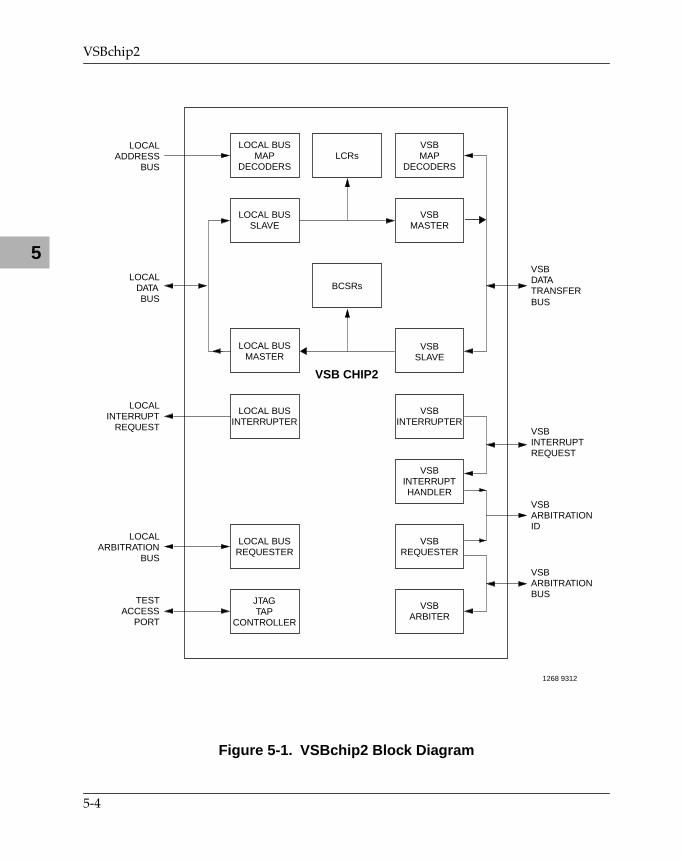
Functional DescriptionThe following sections provide an overview of the functionality of the VSBchip2. See Figure 5-1 for a block diagram of the VSBchip2. Detailed descriptions of all registers are provided later in this chapter.
5-3
VSBchip2
5
Figure 5-1. VSBchip2 Block Diagram
VSBMAP
DECODERS
VSBINTERRUPTHANDLER
LCRs
BCSRs
LOCAL BUSMAP
DECODERS
LOCAL BUSSLAVE
JTAGTAP
CONTROLLER
VSBDATATRANSFERBUS
VSBINTERRUPTREQUEST
VSBARBITRATIONID
VSBARBITRATIONBUS
1268 9312
TESTACCESS
PORT
LOCALARBITRATION
BUS
LOCALINTERRUPT
REQUEST
LOCALDATABUS
LOCALADDRESS
BUS
VSBMASTER
LOCAL BUSMASTER
VSBSLAVE
LOCAL BUSINTERRUPTER
VSBINTERRUPTER
LOCAL BUSREQUESTER
VSBREQUESTER
VSBARBITER
VSB CHIP2
5-4
Functional Description
5
VSB to Local Bus Interface
The VSB to local bus interface allows a VSB device access to local bus resources. This module includes the VSB slave interface, two programmable map decoders, write post buffer, and local bus master interface.
VSB Slave Interface
The VSB slave interface includes one fixed map decoder, two programmable map decoders, and a write post buffer. To support EVSB, the Board Control and Status Registers (BCSRs) are designed to overlay a non-volatile memory which contains board specific information. The VSBchip2 supports this by giving the fixed map decoder precedence over the programmable map decoders. If one of the programmable map decoders is set to respond to an address also covered by the fixed map decoder, the fixed map decoder is the only one to respond.
In some multi-processing situations, it may be beneficial to perform broadcast and broadcall operations. To support this, the VSBchip2 VSB slave interface can be programmed to act as a participating slave as well as a responding slave.
The VSBchip2 can also be programmed to respond to only read transfers, to only write transfers, or to both. Additionally, it can be programmed to reside in any of the three VSB Address Spaces: System (SAS), Alternate (ALTAS), and/or I/O (IOAS).
Programmable Map Decoders
The VSBchip2 includes two programmable map decoders that allow software to configure the VSB addressing range of local bus resources. The decoders allow the local address range to be partitioned into two separate banks, each with its own start and end address (in increments of 64 KB). Each map decoder includes a 16-bit offset register. The contents of the offset register are added to the upper 16 bits of the incoming VSB address before the address is passed on to the local bus master. This allows the address of local resources to differ from their VSB address. Associated with each
5-5
VSBchip2
5
decoder is an attribute register which controls each bank's local bus transfer size, local bus snoop codes, local bus lock, VSB participating/responding slave enable, VSB read enable, VSB write enable, VSB Address Space, and VSB write posting capability.
Write Post Buffer
The VSB slave can be programmed to perform write posting operations. When in this mode, the chip latches incoming VSB data and addressing information into a write post buffer and immediately acknowledges the transfer. The VSB is then free for transfers between other devices while the VSBchip2 requests control of the local bus, waits for a local bus grant, and completes the write transfer. The write post buffer stores the data from one byte, word, or longword data transfer. If any VSB to local bus transfer begins before a previous write-posted cycle has completed, that transfer is not acknowledged until the previous write-posted cycle has completed.
Write posting should only be enabled when bus errors are not expected. Using the programmable map decoders, write posting can be enabled for ÒsafeÓ areas and disabled for areas which are not ÒsafeÓ. If the VSBchip2 detects a bus error during a write posted cycle, this condition is reflected in the Local Interrupt Status Register and the VSB Interrupt Status Register, and a local bus and/or a VSB interrupt may be generated. The address contained in the write post buffer is saved in the VSB Error Address Register, and the specific cause of the error is recorded in the VSB Error Status Register.
Local Bus Master Interface
The local bus master is designed to act exactly as an MC68040 would within the described limits of this chapter. It generates byte, word, and longword single-transfer cycles. It does not generate burst-transfers because there is no equivalent on VSB. The local bus master drives the appropriate local bus snoop control bits and responds to snoop hits correctly.
5-6
Functional Description
5
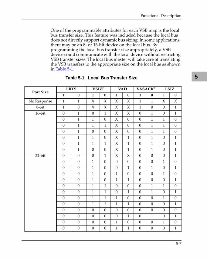
One of the programmable attributes for each VSB map is the local bus transfer size. This feature was included because the local bus does not directly support dynamic bus sizing. In some applications, there may be an 8- or 16-bit device on the local bus. By programming the local bus transfer size appropriately, a VSB device could communicate with the local device without restricting VSB transfer sizes. The local bus master will take care of translating the VSB transfers to the appropriate size on the local bus as shown in Table 5-1.
Table 5-1. Local Bus Transfer Size
Port SizeLBTS VSIZE VAD VASACK* LSIZ
1 0 1 0 1 0 1 0 1 0
No Response 1 1 X X X X 1 1 X X8-bit 1 0 X X X X 1 0 0 116-bit 0 1 0 1 X X 0 1 0 1
0 1 1 0 X 0 0 1 1 00 1 1 1 X 0 0 1 1 00 1 0 0 X 0 0 1 1 00 1 1 0 X 1 0 1 0 10 1 1 1 X 1 0 1 0 10 1 0 0 X 1 0 1 0 1
32-bit 0 0 0 1 X X 0 0 0 10 0 1 0 0 0 0 0 1 00 0 1 0 0 1 0 1 0 10 0 1 0 1 0 0 0 1 00 0 1 0 1 1 0 0 0 10 0 1 1 0 0 0 1 1 00 0 1 1 0 1 0 1 0 10 0 1 1 1 0 0 0 1 00 0 1 1 1 1 0 0 0 10 0 0 0 0 0 0 0 0 00 0 0 0 0 1 0 1 0 10 0 0 0 1 0 0 0 1 00 0 0 0 1 1 0 0 0 1
5-7
VSBchip2
5
VSB Block Transfer to a Local Bus Burst
The VSB slave is capable of receiving VSB block transfer cycles. Each data transfer in the VSB block sequence appears on the local bus as an individual transfer. This is not the most efficient use of VSB block transfers, but unfortunately, because there is no way to know how large the block transfer is going to be, it is not possible to translate these to local bus burst transfers.
Each programmable map can be programmed to lock the local bus during VSB block transfer cycles. This mode can improve data throughput by circumventing the need for local bus arbitration between each data transfer. On VSB it is not possible to determine if a block transfer is in progress until after the first data transfer is complete. After the first data transfer, the negation of PAS* can be used to detect the end of a block. When in local bus lock mode, on the first data transfer of a block, the local bus master acquires the local bus, transfers the data, but does not release the local bus. On subsequent data transfers, the local master can perform transfers without the delay normally caused by acquiring the local bus. After the last cycle of the locked transfer has been completed, the local bus is released.
Note This mode should be used with care. For very long VSB block transfers, local bus devices could be locked off the local bus too long.
Local Bus to VSB Interface
The Local bus to VSB interface allows local bus devices access to resources on the VSB. This module includes the local bus slave interface, four programmable map decoders, a write post buffer, and a VSB master interface.
5-8
Functional Description
5
Local Bus Slave Interface
The local bus slave includes four independent programmable map decoders and two fixed map decoders. The two fixed map decoders are used to decode the addresses of the Local Control and Status Registers (LCSRs) and the Board Control and Status Registers (BCSRs) respectively.
When a local bus address falls within the range of one of the programmable map decoders, the VSBchip2 assumes control over the local bus time-out using its internal VSB access and VSB transfer timers. The local bus slave asserts the LBTODIS* output pin to turn off any external timers for the remainder of this transfer.
Programmable Map Decoders
The VSBchip2 includes four map decoders that allow software to configure the local bus addressing range of VSB resources. The decoders allow the VSB address range to be partitioned into four separate banks, each with its own start and end address (in increments of 64 KB). Each map decoder includes a 16-bit offset register. The contents of the offset register are added to the upper 16 bits of the incoming local bus address before the address is passed on to the VSB master. This allows the address of VSB resources to differ from their local address. Associated with each decoder is an attribute register, which controls each bank's VSB space codes and write posting capability.
Bounce Mode
Bounce mode is a means of prioritizing transfers over VSB and VME, and allows VME and VSB local bus slave mappings to overlap. When bounce mode is enabled, VSB assumes the higher priority, and each transfer is attempted on VSB first. If the transfer fails on VSB, it is then attempted on VME.
If the VSBchip2 local bus slave receives a Òno responseÓ signal back from the VSB master, it can be programmed to carry out one of two courses of action. If bounce mode is enabled, the local bus slave asserts the BOUNCE output pin and negates the LBTODIS* pin
5-9
VSBchip2
5
until it detects the end of the current local bus transfer. If bounce mode is not enabled, the local bus slave asserts LTEA* to terminate the transfer. The BOUNCE output pin is asserted 1 clock after the local bus TS* is detected for cycles which are not decoded by the VSBchip2.
For local bus burst transfers, BOUNCE is asserted only if the Òno responseÓ condition occurred on the first transfer attempt on VSB. On subsequent transfers, the Òno responseÓ condition is treated as a bus error, and the local burst is terminated accordingly.
Write Post Buffer
The local bus slave can be programmed to perform write posting operations. When in this mode, the chip latches incoming local bus data and addressing information into a write post buffer and immediately acknowledges the transfer. The local bus is then free to perform transfers between other devices while the VSBchip2 requests control of the VSB, waits for a VSB grant, and completes the write transfer. The write post buffer stores the data from one byte, word, longword, or burst data transfer. If a local bus write transfer begins before a previous write-posted cycle has completed, that transfer is not acknowledged until the previously write-posted cycle has completed.
Write posting should only be enabled when bus errors are not expected. Normal memory cards never return a bus error on a write cycle. However, some ECC memory cards which reside on VSB perform a read-modify-write operation and therefore may return a bus error if there is an error on the read portion of a read-modify-write. Using the programmable map decoders, write posting can be enabled for ÒsafeÓ areas and disabled for areas which are not ÒsafeÓ. If the VSBchip2 detects a bus error during a write-posted cycle, this condition is reflected in the Local Interrupt Status Register, and a local bus interrupt may be generated. The address contained in the write post buffer is saved in the Local Bus Error Address Register, and the specific cause of the error is recorded in the Chip Control/Status Register.
5-10
Functional Description
5
VSB Master Interface
The VSB master supports data broadcast and data broadcall operations on the VSB. If no VSB device is programmed to respond to the current VSB cycle, the VSB master terminates the VSB cycle and passes this information back to the local bus slave.
VSB Dynamic Bus Sizing
The VSBchip2 supports dynamic bus sizing on the VSB. For example, when a local device initiates a D32 access to a VSB slave that only has D16 data transfer capability, the chip executes two word transfer cycles on the VSB and acknowledges the transfer on the local bus side after all requested data has been transferred. This enhances the portability of software because it allows software to run on the system regardless of the physical organization of global memory.
VSB Timers
There are two programmable timers which control the operation of the VSB master. The VSB access timer measures the time from the VSB master bus request until the VSB requester has gained control of the bus. The VSB transfer timer measures two different periods. During the address broadcast phase, it measures the time from the assertion of VSB address until a VSB device has acknowledged receipt of the address. For the data transfer phase, it measures the time from the beginning of a data transfer until a VSB device has acknowledged the data transfer. Note that for block transfers, the VSB transfer timer starts over at the beginning of each data transfer.
The VSB access timer actually measures the time from the assertion of the VSB master's bus request to the assertion of bus busy by the VSB requester. The VSB transfer timer actually measures the time from assertion of the address on VSB to the receipt of AC high OR at least one ASACK* active and WAIT* high. It also measures the time from the assertion of data (write cycle) or assertion of DS* (read cycle) to the receipt of ACK* low.
5-11
VSBchip2
5
Normally, if the VSB is not too heavily loaded, the VSB arbiter grants the VSB master the bus before the VSB access timer expires. However, for a heavily loaded bus, or for situations where some circuitry may be broken, the VSB access timer expires, and the current access attempt is suspended. If the VSB access timer expires, the appropriate error bit is set in the Chip Control/Status Register, and either the local bus TEA* is asserted to terminate the cycle (no write posting) or the LWPIF bit in the Local Interrupt Status Register is set (write posted cycle). System software must then decide whether to retry the cycle or record the error.
The VSB transfer timer is included to guard against lockup due to certain hardware failures. Normally, the VSB address broadcast phase is terminated when each VSB slave releases AC to high. If, however, any slave continues to drive this signal low, the timer expires, and the transfer is aborted. During the VSB data transfer phase, the responding and/or participating slaves assert ACK* and release WAIT*. If, for some reason, one of these signals is stuck or not driven correctly, the VSB transfer timer expires, and the cycle is aborted. If the VSB transfer timer expires, the appropriate error bit is set in the Chip Control/Status Register, and either the local bus TEA* is asserted to terminate the cycle (no write posting) or the LWPIF bit in the Local Interrupt Status Register is set (write posted cycle).
VSB Block Transfers
The VSBchip2 attempts to generate VSB block transfer cycles when multiple VSB transfers are necessary due to a local bus burst transfer.
Local bus burst cycles are not required to be burst aligned (i. e., on even 16-byte boundaries). The local bus address determines the destination of the first longword. The destination of the next longword is determined by incrementing the address by four, unless incrementing by four would cross an even 16-byte boundary. If a boundary would be crossed, the destination address ÒwrapsÓ back to the previous 16-byte boundary. For example, for a local bus burst which begins at address $00003214, the four longwords would actually be destined for addresses $00003214,
5-12
Functional Description
5
$00003218, $0000321C, $00003210 respectively. Because each VSB block transfer must be to the next linear address, it may be necessary to divide local bus burst transfers into at least two VSB blocks. In the example above, the first three longwords could be sent as a block on VSB, but the fourth longword would require the VSB address to be reissued. Each local bus burst transfer is converted into a VSB block transfer sequence until the address ÒwrapsÓ back to the beginning of the local bus burst boundary. At this point, the VSB address is reissued and a new block begun.
If at any time the responding and/or participating VSB slave wishes to break a block transfer sequence, the VSBchip2 reissues the VSB address and starts another VSB block.
VSB Requester and VSB Serial Arbiter
The VSBchip2 contains all the necessary circuitry to implement a serial VSB requester, a serial VSB arbiter, and a parallel VSB requester. The arbitration mode used is determined by the state of the VPARMD* input pin and the geographical address input pins (VGA2 - VGA0) upon power-up. Parallel VSB requester mode is supported by the MVME166/176.
VSB Geographical Addressing
The VSB specification assigns each slot in a VSB backplane a unique address using the GA2 - GA0 signals. When a board is installed in a backplane slot, it uses the addresses on these lines as part of its interrupt and parallel arbitration IDs and to determine which board contains the active VSB arbiter. In addition, the VSBchip2 uses the geographical address to determine the placement of the Board Control and Status Registers. The VSB specification defines the geographical addresses as follows:
VSB Slot GA2 GA1 GA01 0 0 02 0 0 13 0 1 04 0 1 15 1 0 06 1 0 1
5-13
VSBchip2
5
Note VSB must be implemented using a VSB backplane. A typical VSB backplane presses on the back of the VMEbus backplane behind P2.
The VSBchip2 VGA2 - VGA0 input pins have internal pull-up resistors. If they are not connected to the appropriate VSB geographical addresses, they will always read as %111, an illegal combination according to the VSB specification. In this case, the VSBchip2 assumes it resides in a system without geographical addresses. Parallel arbitration is disabled regardless of the state of the VPARMD* pin, and the serial requester is enabled by default. The VSBchip2 drives VBGOUT* appropriately to configure the rest of the VSB subsystem requesters. The serial arbiter is enabled if software initializes SGA2 - SGA0 in the Chip Control/Status Register to %000. It is the responsibility of the system software to assure that each board in the VSB subsystem is configured with a unique geographical address and that one of those boards is at %000.
If the VGA2 - VGA0 input pins are not %111 after power-up, the VSBchip2 assumes it is in a system with a fully VSB-compliant backplane. If VGA2 - VGA0 are %000, the VSBchip2 samples the VPARMD* input pin to determine the request mode. It then drives the VBGIN*/VBGOUT* daisy chain appropriately to configure the other requesters in the system. If the VPARMD* pin is low, parallel arbitration mode is selected. Systems integrators must be aware that if the board in VSB slot 1 is configured as a parallel requester, all other boards in that VSB subsystem MUST also have parallel requester capability. If serial only boards are placed in a system configured for parallel request mode, the VSB subsystem may become deadlocked.
VSB Requesters
In parallel mode, the VSB requester that currently has the bus performs an arbitration cycle to determine which requesting device gets it next. All requesters that have a request pending participate in the arbitration cycle. There is no parallel arbiter. In serial mode,
5-14
Functional Description
5
each requester submits its bus request to one system arbiter. Only the arbiter in VSB slot 1 (SGA2 - SGA0 are %000) will be the active system arbiter. All other serial arbiters are disabled.
The VSB requester issues a bus request under the following conditions:
The VSB master wishes to perform a VSB cycler, OR
Some external circuitry has asserted the DWB* input pin, OR
System software has set the DWB bit in the VSB Requester Control Register.
The VSB requester may be programmed to implement a ÒfairnessÓ mode to assure that all VSB masters have equal access to the VSB. In fairness mode, any requester which has just released the VSB refrains from requesting it again until VBREQI* is high, indicating no other requests are pending.
When operating in the serial mode, the VSB requester may be programmed to implement one of two different release modes: Release-When-Done (RWD) or Release-On-Request (ROR). Release-When-Done specifies that the requester does not release the bus until its associated master no longer needs it. Release-On-Request means the requester releases the bus only when its associated master no longer needs it AND some other requester has a request pending.
When the VSBchip2 is operating in parallel arbitration mode, the active parallel requester generates a VSB parallel arbitration cycle to transfer bus mastership. Each requester which has a request pending drives a 7-bit arbitration vector onto the VSB data bus. This vector is composed of SGA2 - SGA0 from the Chip Control/Status Register appended to VARBID3 - VARBID0 from the VSB Requester Control/Status Register. The arbitration process is described in the VSB specification, section 3.4.2.
5-15
VSBchip2
5
VSB Serial Arbiter
Only one serial arbiter may be active in a VSB subsystem. The VSBchip2 serial arbiter is active only if SGA2 - SGA0 in the Chip Control/Status Register are %000, and serial arbitration mode is selected by driving the input pin VPARMD* to a high.
Arbitration Timer
The VSBchip2 includes an arbitration timer which measures the time between when its arbiter asserts bus grant and when a VSB requester assumes control of the bus. This timer prevents a bus lock-up condition caused when no requester assumes control of the bus after a grant was issued. When the timer expires, the arbiter asserts bus busy temporarily as if it is the responding requester and then re-arbitrates any pending bus requests. The VARTO bit in the Chip Control/Status Register is set each time the arbitration timer expires. An arbitration time-out is not normally treated as a fatal error condition because the arbitration is retried, but continued time-outs may be an indication of a bad VSB arbiter/requester or an improper subsystem configuration.
VSB Interrupter
The VSBchip2 has two sources for generating a VSB Interrupt: a VSB Write Post Error, and the VSWIF bit in the VSB Interrupt Status Register.
The VSB interrupter generates a VSB Write Post Error interrupt every time a VSB write posted cycle is aborted because of a local bus time-out or bus error if the VGIE and VWPIE bits are set in the VSB Interrupt Enable Register enabling the VSBchip2 to assert the output pin VIRQO*.
When the VSWIF bit in the VSB Interrupt Status Register is set, and the VGIE and VSWIE bits in the VSB Interrupt Enable Register are set, the VSB interrupter generates a VSB interrupt by asserting its output pin VIRQO*.
5-16

Functional Description
5
When the VSB interrupter within the VSBchip2 detects the VSB master is executing a VSB interrupt acknowledge cycle, this interrupter responds with the 8-bit vector contained in the VSB Interrupt Vector Register and then clears the interrupt request. The lowest order bit of the interrupt vector is unique for each interrupt source. The VSBchip2 only responds to an interrupt-acknowledge cycle if the VEN bit in the VSB Interrupt Control Register is set.
If there is no active VSB interrupt handler, the interrupt bits may be polled and cleared by system software.
The VSB interrupter may be programmed to implement a ÒfairnessÓ mode to assure that all VSB interrupters have an equal opportunity to be serviced. In fairness mode, any interrupter which has just been serviced refrains from generating another interrupt until VIRQI* is high, indicating no other interrupt requests are pending.
The address broadcast portion of a VSB interrupt acknowledge is used to determine which interrupt is to be serviced. Each interrupt which has a request pending drives a 7-bit arbitration vector onto the VSB data bus. This vector is composed of SGA2 - SGA0 from the Chip Control/Status Register appended to VINTID3 - VINTID0 from the VSB Interrupt Control Register. The interrupt arbitration process is described in the VSB specification section 2.5.4.
After the highest priority interrupt requester has been selected, that requester uses the data transfer portion of the VSB interrupt acknowledge to pass its vector back to the VSB interrupt handler.
Interrupt Vector Bit 0
Source
0 VSB Write Post Error Interrupt1 Software Interrupt
5-17
VSBchip2
5
VSB Interrupt Handler
The VSB interrupt handler will generate a VSB interrupt acknowledge cycle automatically when it is enabled, a VSB interrupt is pending, and a local bus interrupt acknowledge cycle is performed to service the VSB interrupt. If no VSB interrupter responds to the VSB interrupt acknowledge cycle, an 8-bit vector derived from the Local Interrupt Vector Base Register will be returned. (Refer to the Local Bus Interrupter description that follows.)
System software is responsible for assuring that only one VSB interrupt handler is enabled in a VSB subsystem at any given time.
Local Bus Interrupter
There are five sources of local bus interrupts: Local Write Post Error, VSB Write Post Error, VSB Interrupt Pending, EVSB Attention Interrupt, and VSB Interrupt Acknowledge Complete. Any of these sources can be programmed to generate a local bus interrupt at any level.
When an interrupt acknowledge cycle is executed to service these interrupts, the vector driven onto the local bus is derived from the Local Bus Interrupt Vector Register as shown below.
A Local Write Post Error interrupt is generated any time an error is detected during completion of a local bus transfer which has been write posted. This interrupt is cleared either automatically when serviced by a local bus interrupt acknowledge cycle or under software control.
Interrupt Vector Bits 3-0 Source
$0 Local Write Post Error Interrupt$1 VSB Write Post Interrupt$2 VSB Interrupt Pending$4 EVSB Attention Interrupt$5 VSB Interrupt Acknowledge Complete
5-18
Functional Description
5
A VSB Write Post Error interrupt is generated any time an error is detected during completion of a VSB transfer which has been write posted. This interrupt is cleared either automatically when serviced by a local bus interrupt acknowledge cycle or under software control.
A VSB IRQ Pending interrupt is generated any time the VSB IRQ signal is asserted. This interrupt can be cleared only by clearing the source of the interrupt on VSB. When this interrupt is serviced by a local bus interrupt acknowledge cycle, the source of the returned vector is programmable. If the VSB interrupt handler is enabled, it performs an interrupt acknowledge cycle on the VSB and passes the resulting vector back to the local bus. If the VSB interrupt handler is disabled or the VSB interrupt acknowledge cycle is unsuccessful, the vector driven onto the local bus is derived from the Local Bus Interrupt Vector Register as shown above.
An EVSB Attention interrupt is generated when the ATTN bit in the EVSB Attention Register is set. This interrupt is cleared either automatically when serviced by a local bus interrupt acknowledge cycle or under software control.
A VSB Interrupt Acknowledge Complete Interrupt is generated when the VSWIF bit in the VSB Interrupt Status Register is cleared. This interrupt is cleared either automatically when serviced by a local bus interrupt acknowledge cycle or under software control.
The VSBchip2 includes the means to merge an externally generated prioritized interrupt with those generated internally. When an ex- ternal interrupt is detected on pins LIPLI2 - LIPLI0, its priority level is compared to any pending internal interrupts, and the highest priority level is output on the local bus interrupt level pins LIPLO2 - LIPLO0. This interrupt must be serviced and cleared at its source.
Control and Status Registers
The VSBchip2 includes two sets of registers. The Local Control/Status Registers are accessible only from the local bus. These registers are described in detail next in this chapter. The Board Control/Status Registers are accessible from both the local bus and VSB. These registers are described in detail later in this chapter.
5-19
VSBchip2
5
Local Control and Status Registers Programming Model
The VSBchip2 contains 23 Local Bus Control and Status Registers (LCSRs). These LCSRs are accessible only through the local bus interface. Each register can be read or written by a byte, word, or longword single-transfer cycle. If a burst transfer is used to read from or write to these registers, the first transfer completes successfully and the VSBchip2 asserts LTBI* on the local bus to indicate it cannot complete the rest of the request. Table 5-2 summarizes this register set.
Each register is defined by a table with five lines: an ADR/SIZ field, BIT field, NAME field, OPER field, and RESET field. The ADR/SIZ field defines the base address of the register and the number of bits defined in the table. The BIT field specifies the function's bit location in the register, and the NAME field is the name of the function. Unused bits have the word 'Reserved' in their NAME field. For these bits, writes have no effect and reads always return a zero. The OPER field specifies the allowed operations on that function. These operations are:
The last field, RESET, specifies both the state the bit enters upon application of a reset, and by which reset signal(s) it is affected. The three reset states are 0, 1, or the letter `X' (not affected). The two reset signals are power-up reset (PURST*) signified by the letter 'P', or a local reset (LBRSTI*) signified by the letter 'L'.
R This bit is read only.
R/W This bit is read and write.
R/C This bit is read and clear only.
R/S This bit is read and set only.
5-20
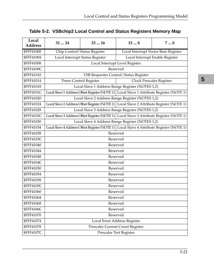
Local Control and Status Registers Programming Model
5
Table 5-2. VSBchip2 Local Control and Status Registers Memory Map
Local Address
31 ... 24 23 ... 16 15 ... 8 7 ... 0
$FFF41000 Chip Control/Status Register Local Interrupt Vector Base Register
$FFF41004 Local Interrupt Status Register Local Interrupt Enable Register
$FFF41008 Local Interrupt Level Register
$FFF4100C Reserved
$FFF41010 VSB Requester Control/Status Register
$FFF41014 Timer Control Register Clock Prescaler Register
$FFF41018 Local Slave 1 Address Range Register (NOTES 1,2)
$FFF4101C Local Slave 1 Address Offset Register (NOTE 1) Local Slave 1 Attribute Register (NOTE 1)
$FFF41020 Local Slave 2 Address Range Register (NOTES 1,2)
$FFF41024 Local Slave 2 Address Offset Register (NOTE 1) Local Slave 2 Attribute Register (NOTE 1)
$FFF41028 Local Slave 3 Address Range Register (NOTES 1,2)
$FFF4102C Local Slave 3 Address Offset Register (NOTE 1) Local Slave 3 Attribute Register (NOTE 1)
$FFF41030 Local Slave 4 Address Range Register (NOTES 1,2)
$FFF41034 Local Slave 4 Address Offset Register (NOTE 1) Local Slave 4 Attribute Register (NOTE 1)
$FFF41038 Reserved
$FFF4103C Reserved
$FFF41040 Reserved
$FFF41044 Reserved
$FFF41048 Reserved
$FFF4104C Reserved
$FFF41050 Reserved
$FFF41054 Reserved
$FFF41058 Reserved
$FFF4105C Reserved
$FFF41060 Reserved
$FFF41064 Reserved
$FFF41068 Reserved
$FFF4106C Reserved
$FFF41070 Reserved
$FFF41074 Local Error Address Register
$FFF41078 Prescaler Current Count Register
$FFF4107C Prescaler Test Register
5-21
VSBchip2
5
Notes 1. Registers listed as ÒSlaveÓ 1, 2, 3, or 4 in this memory map are listed as ÒMasterÓ 1, 2, 3, or 4 in the ENV command parameters configurable by MVME166BUG (166Bug) or MVME176BUG (176Bug).
2. Registers listed as ÒSlave Address RangeÓ in this memory map are listed as ÒMaster Starting AddressÓ and ÒMaster Ending AddressÓ in the ENV command parameters configurable by 166/176Bug).
5-22
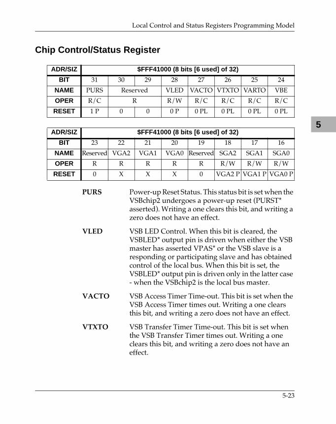
Local Control and Status Registers Programming Model
5
Chip Control/Status Register
PURS Power-up Reset Status. This status bit is set when the VSBchip2 undergoes a power-up reset (PURST* asserted). Writing a one clears this bit, and writing a zero does not have an effect.
VLED VSB LED Control. When this bit is cleared, the VSBLED* output pin is driven when either the VSB master has asserted VPAS* or the VSB slave is a responding or participating slave and has obtained control of the local bus. When this bit is set, the VSBLED* output pin is driven only in the latter case - when the VSBchip2 is the local bus master.
VACTO VSB Access Timer Time-out. This bit is set when the VSB Access Timer times out. Writing a one clears this bit, and writing a zero does not have an effect.
VTXTO VSB Transfer Timer Time-out. This bit is set when the VSB Transfer Timer times out. Writing a one clears this bit, and writing a zero does not have an effect.
ADR/SIZ $FFF41000 (8 bits [6 used] of 32)
BIT 31 30 29 28 27 26 25 24
NAME PURS Reserved VLED VACTO VTXTO VARTO VBE
OPER R/C R R/W R/C R/C R/C R/C
RESET 1 P 0 0 0 P 0 PL 0 PL 0 PL 0 PL
ADR/SIZ $FFF41000 (8 bits [6 used] of 32)
BIT 23 22 21 20 19 18 17 16
NAME Reserved VGA2 VGA1 VGA0 Reserved SGA2 SGA1 SGA0
OPER R R R R R R/W R/W R/W
RESET 0 X X X 0 VGA2 P VGA1 P VGA0 P
5-23
VSBchip2
5
VARTO VSB Arbitration Timer Time-out. This bit is set when the VSB Arbitration Timer times out. Writing a one clears this bit, and writing a zero does not have an effect.
VBE VSB Bus Error. This bit is set when the VSB master detects one of the following three conditions:
1. The VSB responding slave answers by asserting VERRI*.
2. A VSB responding slave is not found at the requested address when bounce mode is disabled.
3. A VSB responding slave does not continue to respond at the requested address after some part of the requested transfer has been completed.
Writing a one clears this bit, and writing a zero does not have an effect.
VGA2 - VGA0 VSB Geographical Address. These bits reflect the status of the VGA2 - VGA0 input pins. An address of %111 indicates that the board is not plugged into a VSB backplane.
SGA2 - SGA0 Programmable Geographical Address. Software can change the board's geographical address by programming these bits. When changing a board's geographical address, the burden is now on the system programmer to ensure that each board in the VSB subsystem is assigned a unique geographical address. On power-up, these bits revert to state of the VGA2 - VGA0 input pins.
5-24
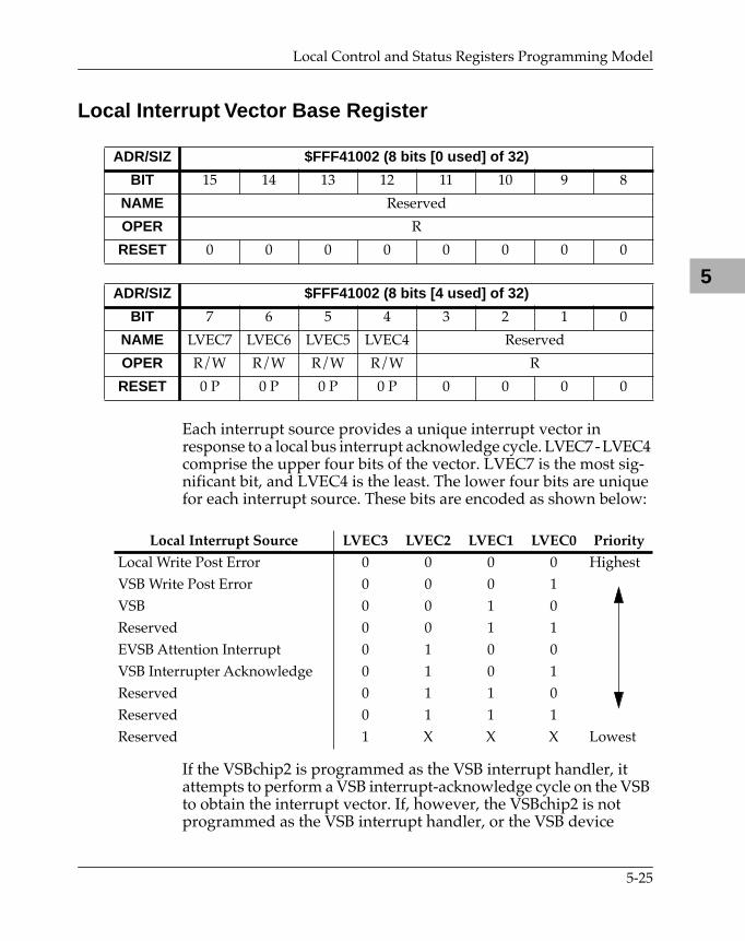
Local Control and Status Registers Programming Model
5
Local Interrupt Vector Base Register
Each interrupt source provides a unique interrupt vector in response to a local bus interrupt acknowledge cycle. LVEC7 - LVEC4 comprise the upper four bits of the vector. LVEC7 is the most sig- nificant bit, and LVEC4 is the least. The lower four bits are unique for each interrupt source. These bits are encoded as shown below:
If the VSBchip2 is programmed as the VSB interrupt handler, it attempts to perform a VSB interrupt-acknowledge cycle on the VSB to obtain the interrupt vector. If, however, the VSBchip2 is not programmed as the VSB interrupt handler, or the VSB device
ADR/SIZ $FFF41002 (8 bits [0 used] of 32)
BIT 15 14 13 12 11 10 9 8
NAME Reserved
OPER R
RESET 0 0 0 0 0 0 0 0
ADR/SIZ $FFF41002 (8 bits [4 used] of 32)
BIT 7 6 5 4 3 2 1 0
NAME LVEC7 LVEC6 LVEC5 LVEC4 Reserved
OPER R/W R/W R/W R/W R
RESET 0 P 0 P 0 P 0 P 0 0 0 0
Local Interrupt Source LVEC3 LVEC2 LVEC1 LVEC0 Priority
Local Write Post Error 0 0 0 0 HighestVSB Write Post Error 0 0 0 1VSB 0 0 1 0Reserved 0 0 1 1EVSB Attention Interrupt 0 1 0 0VSB Interrupter Acknowledge 0 1 0 1Reserved 0 1 1 0Reserved 0 1 1 1Reserved 1 X X X Lowest
5-25
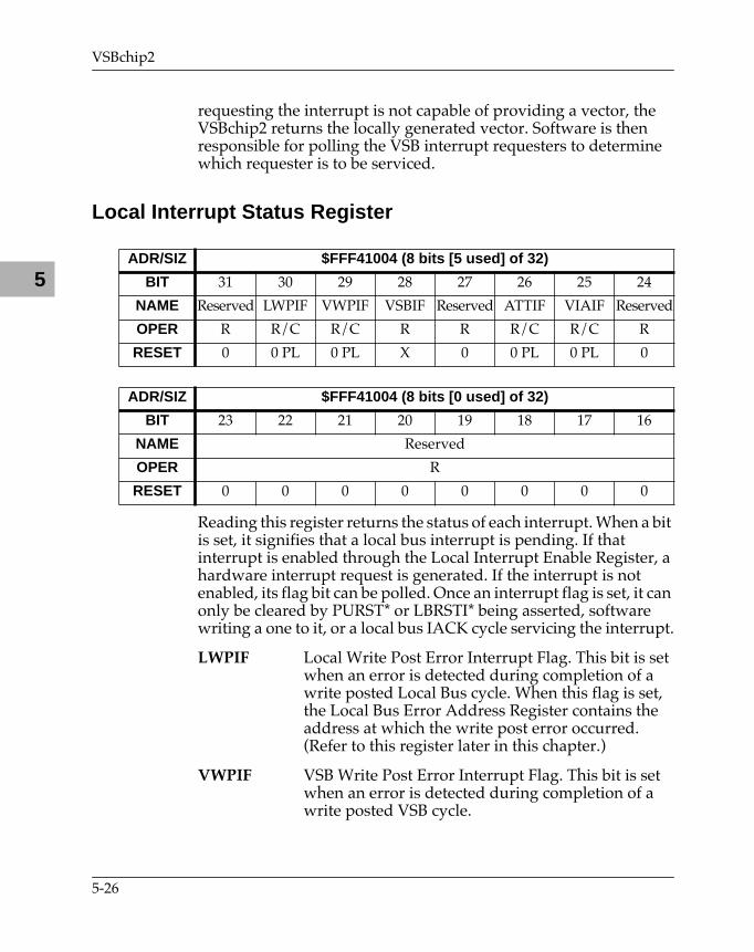
VSBchip2
5
requesting the interrupt is not capable of providing a vector, the VSBchip2 returns the locally generated vector. Software is then responsible for polling the VSB interrupt requesters to determine which requester is to be serviced.
Local Interrupt Status Register
Reading this register returns the status of each interrupt. When a bit is set, it signifies that a local bus interrupt is pending. If that interrupt is enabled through the Local Interrupt Enable Register, a hardware interrupt request is generated. If the interrupt is not enabled, its flag bit can be polled. Once an interrupt flag is set, it can only be cleared by PURST* or LBRSTI* being asserted, software writing a one to it, or a local bus IACK cycle servicing the interrupt.
LWPIF Local Write Post Error Interrupt Flag. This bit is set when an error is detected during completion of a write posted Local Bus cycle. When this flag is set, the Local Bus Error Address Register contains the address at which the write post error occurred. (Refer to this register later in this chapter.)
VWPIF VSB Write Post Error Interrupt Flag. This bit is set when an error is detected during completion of a write posted VSB cycle.
ADR/SIZ $FFF41004 (8 bits [5 used] of 32)
BIT 31 30 29 28 27 26 25 24
NAME Reserved LWPIF VWPIF VSBIF Reserved ATTIF VIAIF Reserved
OPER R R/C R/C R R R/C R/C R
RESET 0 0 PL 0 PL X 0 0 PL 0 PL 0
ADR/SIZ $FFF41004 (8 bits [0 used] of 32)
BIT 23 22 21 20 19 18 17 16
NAME Reserved
OPER R
RESET 0 0 0 0 0 0 0 0
5-26
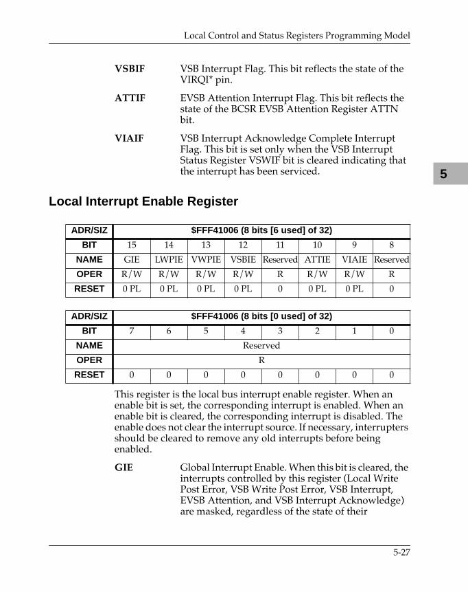
Local Control and Status Registers Programming Model
5
VSBIF VSB Interrupt Flag. This bit reflects the state of the VIRQI* pin.
ATTIF EVSB Attention Interrupt Flag. This bit reflects the state of the BCSR EVSB Attention Register ATTN bit.
VIAIF VSB Interrupt Acknowledge Complete Interrupt Flag. This bit is set only when the VSB Interrupt Status Register VSWIF bit is cleared indicating that the interrupt has been serviced.
Local Interrupt Enable Register
This register is the local bus interrupt enable register. When an enable bit is set, the corresponding interrupt is enabled. When an enable bit is cleared, the corresponding interrupt is disabled. The enable does not clear the interrupt source. If necessary, interrupters should be cleared to remove any old interrupts before being enabled.
GIE Global Interrupt Enable. When this bit is cleared, the interrupts controlled by this register (Local Write Post Error, VSB Write Post Error, VSB Interrupt, EVSB Attention, and VSB Interrupt Acknowledge) are masked, regardless of the state of their
ADR/SIZ $FFF41006 (8 bits [6 used] of 32)
BIT 15 14 13 12 11 10 9 8
NAME GIE LWPIE VWPIE VSBIE Reserved ATTIE VIAIE Reserved
OPER R/W R/W R/W R/W R R/W R/W R
RESET 0 PL 0 PL 0 PL 0 PL 0 0 PL 0 PL 0
ADR/SIZ $FFF41006 (8 bits [0 used] of 32)
BIT 7 6 5 4 3 2 1 0
NAME Reserved
OPER R
RESET 0 0 0 0 0 0 0 0
5-27
VSBchip2
5
individual enable bits. When this bit is set, the five interrupts are not masked and can be enabled by setting their enable bit.
LWPIE Local Write Post Error Interrupt Enable. When this bit and the GIE bit are set, whenever the LWPIF bit in the Local Interrupt Status Register is set, an interrupt is generated on the local bus by asserting its interrupt level programmed in the Local Interrupt Level Register on the output pins LIPLO2*-LIPLO0*.
VWPIE VSB Write Post Error Interrupt Enable. When this bit and the GIE bit are set, whenever the VWPIF bit in the Local Interrupt Status Register is set, an interrupt is generated on the local bus by asserting its interrupt level programmed in the Local Interrupt Level Register on the output pins LIPLO2*-LIPLO0*.
VSBIE VSB Interrupt Enable. When this bit and the GIE bit are set, whenever the VSBIF bit in the Local Interrupt Status Register is set, an interrupt is generated on the local bus by asserting its interrupt level programmed in the Local Interrupt Level Register on the output pins LIPLO2*-LIPLO0*.
ATTIE EVSB Attention Interrupt Enable. When this bit and the GIE bit are set, whenever the ATTIF bit in the Local Interrupt Status Register is set, an interrupt is generated on the local bus by asserting its interrupt level programmed in the Local Interrupt Level Register on the output pins LIPLO2*-LIPLO0*.
VIAIE VSB Interrupt Acknowledge Complete Interrupt Enable. When this bit and the GIE bit are set, whenever the VIAIF bit in the Local Interrupt Status Register is set, an interrupt is generated on the local bus by asserting its interrupt level programmed in the Local Interrupt Level Register on the output pins LIPLO2*-LIPLO0*.
5-28
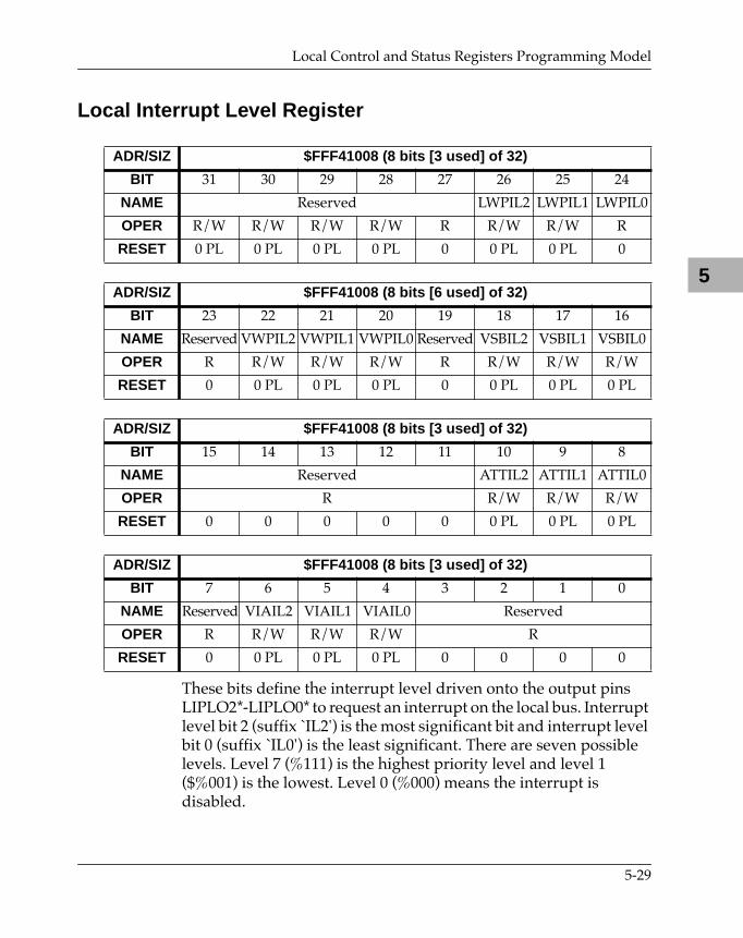
Local Control and Status Registers Programming Model
5
Local Interrupt Level Register
These bits define the interrupt level driven onto the output pins LIPLO2*-LIPLO0* to request an interrupt on the local bus. Interrupt level bit 2 (suffix ̀ IL2') is the most significant bit and interrupt level bit 0 (suffix `IL0') is the least significant. There are seven possible levels. Level 7 (%111) is the highest priority level and level 1 ($%001) is the lowest. Level 0 (%000) means the interrupt is disabled.
ADR/SIZ $FFF41008 (8 bits [3 used] of 32)
BIT 31 30 29 28 27 26 25 24
NAME Reserved LWPIL2 LWPIL1 LWPIL0
OPER R/W R/W R/W R/W R R/W R/W R
RESET 0 PL 0 PL 0 PL 0 PL 0 0 PL 0 PL 0
ADR/SIZ $FFF41008 (8 bits [6 used] of 32)
BIT 23 22 21 20 19 18 17 16
NAME Reserved VWPIL2 VWPIL1 VWPIL0 Reserved VSBIL2 VSBIL1 VSBIL0
OPER R R/W R/W R/W R R/W R/W R/W
RESET 0 0 PL 0 PL 0 PL 0 0 PL 0 PL 0 PL
ADR/SIZ $FFF41008 (8 bits [3 used] of 32)
BIT 15 14 13 12 11 10 9 8
NAME Reserved ATTIL2 ATTIL1 ATTIL0
OPER R R/W R/W R/W
RESET 0 0 0 0 0 0 PL 0 PL 0 PL
ADR/SIZ $FFF41008 (8 bits [3 used] of 32)
BIT 7 6 5 4 3 2 1 0
NAME Reserved VIAIL2 VIAIL1 VIAIL0 Reserved
OPER R R/W R/W R/W R
RESET 0 0 PL 0 PL 0 PL 0 0 0 0
5-29
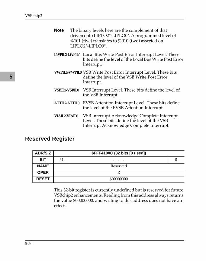
VSBchip2
5
Note The binary levels here are the complement of that driven onto LIPLO2*-LIPLO0*. A programmed level of %101 (five) translates to %010 (two) asserted on LIPLO2*-LIPLO0*.
LWPIL2-LWPIL0 Local Bus Write Post Error Interrupt Level. These bits define the level of the Local Bus Write Post Error Interrupt.
VWPIL2-VWPIL0 VSB Write Post Error Interrupt Level. These bits define the level of the VSB Write Post Error Interrupt.
VSBIL2-VSBIL0 VSB Interrupt Level. These bits define the level of the VSB Interrupt.
ATTIL2-ATTIL0 EVSB Attention Interrupt Level. These bits define the level of the EVSB Attention Interrupt.
VIAIL2-VIAIL0 VSB Interrupt Acknowledge Complete Interrupt Level. These bits define the level of the VSB Interrupt Acknowledge Complete Interrupt.
Reserved Register
This 32-bit register is currently undefined but is reserved for future VSBchip2 enhancements. Reading from this address always returns the value $00000000, and writing to this address does not have an effect.
ADR/SIZ $FFF4100C (32 bits [0 used])
BIT 31 . . . 0
NAME Reserved
OPER R
RESET $00000000
5-30
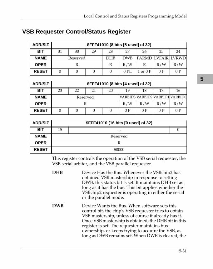
Local Control and Status Registers Programming Model
5
VSB Requester Control/Status Register
This register controls the operation of the VSB serial requester, the VSB serial arbiter, and the VSB parallel requester.
DHB Device Has the Bus. Whenever the VSBchip2 has obtained VSB mastership in response to setting DWB, this status bit is set. It maintains DHB set as long as it has the bus. This bit applies whether the VSBchip2 requester is operating in either the serial or the parallel mode.
DWB Device Wants the Bus. When software sets this control bit, the chip's VSB requester tries to obtain VSB mastership, unless of course it already has it. Once VSB mastership is obtained, the DHB bit in this register is set. The requester maintains bus ownership, or keeps trying to acquire the VSB, as long as DWB remains set. When DWB is cleared, the
ADR/SIZ $FFF41010 (8 bits [5 used] of 32)
BIT 31 30 29 28 27 26 25 24
NAME Reserved DHB DWB PARMD LVFAIR LVRWD
OPER R R R/W R R/W R/W
RESET 0 0 0 0 0 PL 1 or 0 P 0 P 0 P
ADR/SIZ $FFF41010 (8 bits [4 used] of 32)
BIT 23 22 21 20 19 18 17 16
NAME Reserved VARBID3 VARBID2 VARBID1 VARBID0
OPER R R/W R/W R/W R/W
RESET 0 0 0 0 0 P 0 P 0 P 0 P
ADR/SIZ $FFF41010 (16 bits [0 used] of 32)
BIT 15 ... 0
NAME Reserved
OPER R
RESET $0000
5-31
VSBchip2
5
requester relinquishes control of the VSB. Refer to the section on the VSB Requester and VSB Serial Arbiter (earlier in this chapter) for a discussion of how the VSBchip2 releases the bus when operating in serial or parallel arbitration mode.
PARMD Parallel Arbitration Mode. This status bit reflects the VSB arbitration mode selected on power-up. If the bit is set, the arbitration mode on the VSB is parallel. If the bit is cleared, the arbitration mode is serial. Refer to the section on VSB Geographical Addressing (earlier in this chapter) for the methodology used in selecting the VSB arbitration mode.
LVFAIR VSB Requester Fair Mode. When LVFAIR is set, the VSB Requester waits to assert its contribution to VBREQO* until it detects VBREQI* high for at least 1.5 LBCLK periods since it was last VSB master. When this bit is cleared, the requester does not wait. This bit is applicable only when the requester is operating in the serial arbitration mode.
LVRWD VSB Requester Release When Done. When this bit is set, the requester operates in the Release When Done (RWD) mode. When this bit is cleared, the requester operates in the Release On Request (ROR) mode. This bit is applicable only when the VSBchip2 is operating in the serial arbitration mode.
VARBID3 - VSB Requester Arbitration ID. These four bits are the
VARBID0 upper four bits of the seven bit arbitration ID that the VSB requester places on the VSB when it contends for VSB mastership. The lower 3 bits of the arbitration ID are this board's geographical address. These bits apply only when the requester is operating in the parallel mode. VARBID3 is the most significant bit; and VARBID0 is the least. On power-up reset, these bits are cleared.
5-32
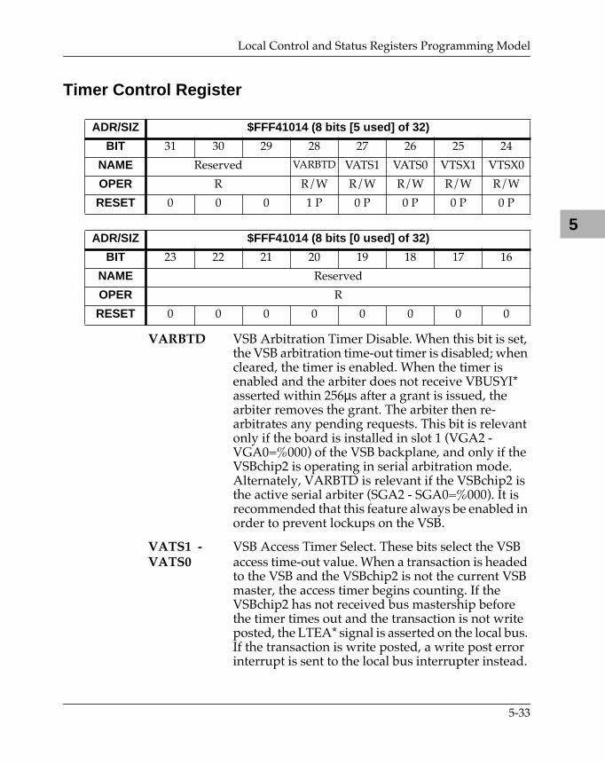
Local Control and Status Registers Programming Model
5
Timer Control Register
VARBTD VSB Arbitration Timer Disable. When this bit is set, the VSB arbitration time-out timer is disabled; when cleared, the timer is enabled. When the timer is enabled and the arbiter does not receive VBUSYI* asserted within 256µs after a grant is issued, the arbiter removes the grant. The arbiter then re-arbitrates any pending requests. This bit is relevant only if the board is installed in slot 1 (VGA2 - VGA0=%000) of the VSB backplane, and only if the VSBchip2 is operating in serial arbitration mode. Alternately, VARBTD is relevant if the VSBchip2 is the active serial arbiter (SGA2 - SGA0=%000). It is recommended that this feature always be enabled in order to prevent lockups on the VSB.
VATS1 - VSB Access Timer Select. These bits select the VSBVATS0 access time-out value. When a transaction is headed
to the VSB and the VSBchip2 is not the current VSB master, the access timer begins counting. If the VSBchip2 has not received bus mastership before the timer times out and the transaction is not write posted, the LTEA* signal is asserted on the local bus. If the transaction is write posted, a write post error interrupt is sent to the local bus interrupter instead.
ADR/SIZ $FFF41014 (8 bits [5 used] of 32)
BIT 31 30 29 28 27 26 25 24
NAME Reserved VARBTD VATS1 VATS0 VTSX1 VTSX0
OPER R R/W R/W R/W R/W R/W
RESET 0 0 0 1 P 0 P 0 P 0 P 0 P
ADR/SIZ $FFF41014 (8 bits [0 used] of 32)
BIT 23 22 21 20 19 18 17 16
NAME Reserved
OPER R
RESET 0 0 0 0 0 0 0 0
5-33
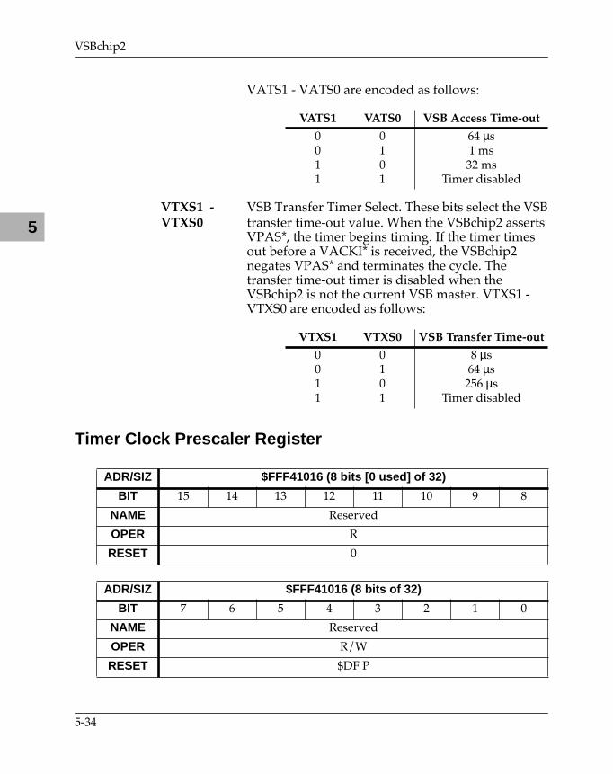
VSBchip2
5
VATS1 - VATS0 are encoded as follows:
VTXS1 - VSB Transfer Timer Select. These bits select the VSBVTXS0 transfer time-out value. When the VSBchip2 asserts
VPAS*, the timer begins timing. If the timer times out before a VACKI* is received, the VSBchip2 negates VPAS* and terminates the cycle. The transfer time-out timer is disabled when the VSBchip2 is not the current VSB master. VTXS1 - VTXS0 are encoded as follows:
Timer Clock Prescaler Register
VATS1 VATS0 VSB Access Time-out
0011
0101
64 µs1 ms32 ms
Timer disabled
VTXS1 VTXS0 VSB Transfer Time-out
0011
0101
8 µs64 µs256 µs
Timer disabled
ADR/SIZ $FFF41016 (8 bits [0 used] of 32)
BIT 15 14 13 12 11 10 9 8
NAME Reserved
OPER R
RESET 0
ADR/SIZ $FFF41016 (8 bits of 32)
BIT 7 6 5 4 3 2 1 0
NAME Reserved
OPER R/W
RESET $DF P
5-34
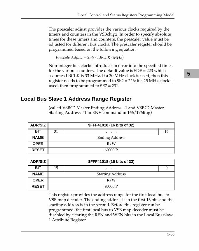
Local Control and Status Registers Programming Model
5
The prescaler adjust provides the various clocks required by the timers and counters in the VSBchip2. In order to specify absolute times for these timers and counters, the prescaler value must be adjusted for different bus clocks. The prescaler register should be programmed based on the following equation:
Prescale Adjust = 256 - LBCLK (MHz)
Non-integer bus clocks introduce an error into the specified times for the various counters. The default value is $DF = 223 which assumes LBCLK is 33 MHz. If a 30 MHz clock is used, then this register needs to be programmed to $E2 = 226; if a 25 MHz clock is used, then programmed to $E7 = 231.
Local Bus Slave 1 Address Range Register
(called VSBC2 Master Ending Address #1 and VSBC2 Master Starting Address #1 in ENV command in 166/176Bug)
This register provides the address range for the first local bus to VSB map decoder. The ending address is in the first 16 bits and the starting address is in the second. Before this register can be programmed, the first local bus to VSB map decoder must be disabled by clearing the REN and WEN bits in the Local Bus Slave 1 Attribute Register.
ADR/SIZ $FFF41018 (16 bits of 32)
BIT 31 . . . 16
NAME Ending Address
OPER R/W
RESET $0000 P
ADR/SIZ $FFF41018 (16 bits of 32)
BIT 15 . . . 0
NAME Starting Address
OPER R/W
RESET $0000 P
5-35
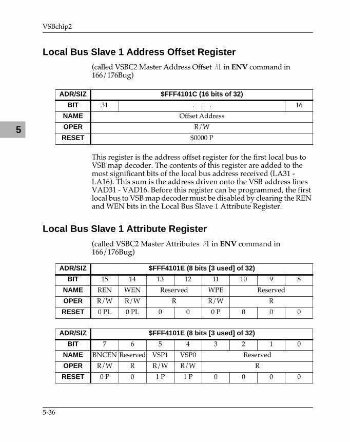
5
VSBchip2
5-36
5VSBchip2
0Local Control and Status Registers Programming Model
Local Bus Slave 1 Address Offset Register
(called VSBC2 Master Address Offset #1 in ENV command in 166/176Bug)
This register is the address offset register for the first local bus to VSB map decoder. The contents of this register are added to the most significant bits of the local bus address received (LA31 - LA16). This sum is the address driven onto the VSB address lines VAD31 - VAD16. Before this register can be programmed, the first local bus to VSB map decoder must be disabled by clearing the REN and WEN bits in the Local Bus Slave 1 Attribute Register.
Local Bus Slave 1 Attribute Register
(called VSBC2 Master Attributes #1 in ENV command in 166/176Bug)
ADR/SIZ $FFF4101C (16 bits of 32)
BIT 31 . . . 16
NAME Offset Address
OPER R/W
RESET $0000 P
ADR/SIZ $FFF4101E (8 bits [3 used] of 32)
BIT 15 14 13 12 11 10 9 8
NAME REN WEN Reserved WPE Reserved
OPER R/W R/W R R/W R
RESET 0 PL 0 PL 0 0 0 P 0 0 0
ADR/SIZ $FFF4101E (8 bits [3 used] of 32)
BIT 7 6 5 4 3 2 1 0
NAME BNCEN Reserved VSP1 VSP0 Reserved
OPER R/W R R/W R/W R
RESET 0 P 0 1 P 1 P 0 0 0 0
Local Control and Status Registers Programming Model
5
REN Read Enable. When this bit is set, the first local bus to VSB map decoder is enabled for read cycles.
WEN Write Enable. When this bit is set, the first local bus to VSB map decoder is enabled for write cycles.
WPE Write Post Enable. When this bit is high, write posting is enabled for the address segment defined by the Local Bus Slave 1 Address Range Register.
BNCEN Bounce Mode Enable. If this bit is set, whenever the VSBchip2 performs a VSB address broadcast in which no slave responds, it asserts the BOUNCE output pin for one LBCLK, terminates the VSB cycle, and waits for an alternate device to terminate the local bus cycle. When bounce is disabled, if there is no response from a VSB slave, the VSBchip2 terminates the local bus transfer by asserting LTEA*.
VSP1 - VSP0 VSB Space Codes. These bits control the space codes asserted by the VSBchip2 when functioning as the VSB master in the address range defined by the Local Bus Slave 1 Address Range Register. VSP1 and VSP0 are encoded as follows:
Address Space VSP1 VSP0
Reserved - System Address Space Selected 0 0Alternate Address Space 0 1I/O Address Space 1 0System Address Space 1 1
5-37
VSBchip2
5
Local Bus Slave 2 Address Range Register
(called VSBC2 Master Ending Address #2 and VSBC2 Master Starting Address #2 in ENV command in 166/176Bug)
This register provides the address range for the second local bus to VSB map decoder. The ending address is in the first 16 bits and the starting address is in the second. Before this register can be programmed, the second local bus to VSB map decoder must be disabled by clearing the REN and WEN bits in the Local Bus Slave 2 Attribute Register.
ADR/SIZ $FFF41020 (16 bits of 32)
BIT 31 . . . 16
NAME Ending Address
OPER R/W
RESET $0000 P
ADR/SIZ $FFF41020 (16 bits of 32)
BIT 15 . . . 0
NAME Starting Address
OPER R/W
RESET $0000 P
5-38
Local Control and Status Registers Programming Model
5
Local Bus Slave 2 Address Offset Register
(called VSBC2 Master Address Offset #2 in ENV command in 166/176Bug)
This register is the address offset register for the second local bus to VSB map decoder. The contents of this register are added to the most significant bits of the local bus address received (LA31 - LA16). This sum is the address driven onto the VSB address lines VAD31 - VAD16. Before this register can be programmed, the second local bus to VSB map decoder must be disabled by clearing the REN and WEN bits in the Local Bus Slave 2 Attribute Register.
Local Bus Slave 2 Attribute Register
(called VSBC2 Master Attributes #2 in ENV command in 166/176Bug)
ADR/SIZ $FFF41024 (16 bits of 32)
BIT 31 . . . 16
NAME Offset Address
OPER R/W
RESET $0000 P
ADR/SIZ $FFF41026 (8 bits [3 used] of 32)
BIT 15 14 13 12 11 10 9 8
NAME REN WEN Reserved WPE Reserved
OPER R/W R/W R R/W R
RESET 0 PL 0 PL 0 0 0 P 0 0 0
ADR/SIZ $FFF41026 (8 bits [3 used] of 32)
BIT 7 6 5 4 3 2 1 0
NAME BNCEN Reserved VSP1 VSP0 Reserved
OPER R/W R R/W R/W R
RESET 0 P 0 1 P 1 P 0 0 0 0
5-39
VSBchip2
5
REN Read Enable. When this bit is set, the second local bus to VSB map decoder is enabled for read cycles.
WEN Write Enable. When this bit is set, the second local bus to VSB map decoder is enabled for write cycles.
WPE Write Post Enable. When this bit is high, write posting is enabled for the address segment defined by the Local Bus Slave 2 Address Range Register.
BNCEN Bounce Mode Enable. If this bit is set, whenever the VSBchip2 performs a VSB address broadcast in which no slave responds, it asserts the BOUNCE output pin for one LBCLK, terminates the VSB cycle, and waits for an alternate device to terminate the local bus cycle. When bounce is disabled, if there is no response from a VSB slave, the VSBchip2 terminates the local bus transfer by asserting LTEA*.
VSP1 - VSP0 VSB Space Codes. These bits control the space codes asserted by the VSBchip2 when functioning as the VSB master in the address range defined by the Local Bus Slave 2 Address Range Register. VSP1 and VSP0 are encoded as follows:
Address Space VSP1 VSP0
Reserved - System Address Space Selected 0 0Alternate Address Space 0 1I/O Address Space 1 0System Address Space 1 1
5-40
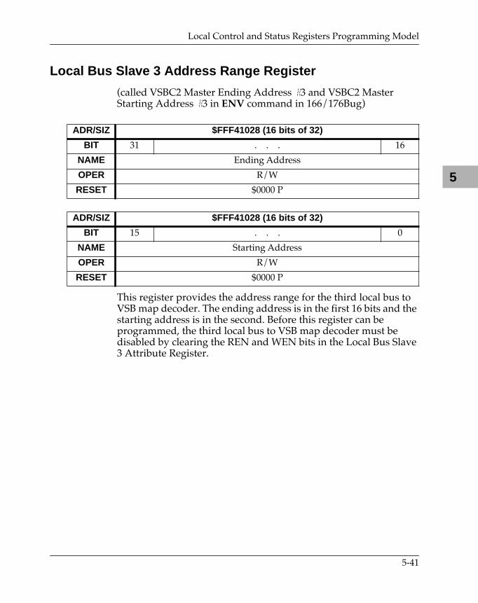
Local Control and Status Registers Programming Model
5
Local Bus Slave 3 Address Range Register
(called VSBC2 Master Ending Address #3 and VSBC2 Master Starting Address #3 in ENV command in 166/176Bug)
This register provides the address range for the third local bus to VSB map decoder. The ending address is in the first 16 bits and the starting address is in the second. Before this register can be programmed, the third local bus to VSB map decoder must be disabled by clearing the REN and WEN bits in the Local Bus Slave 3 Attribute Register.
ADR/SIZ $FFF41028 (16 bits of 32)
BIT 31 . . . 16
NAME Ending Address
OPER R/W
RESET $0000 P
ADR/SIZ $FFF41028 (16 bits of 32)
BIT 15 . . . 0
NAME Starting Address
OPER R/W
RESET $0000 P
5-41

VSBchip2
5
Local Bus Slave 3 Address Offset Register
(called VSBC2 Master Address Offset #3 in ENV command in 166/176Bug)
This register is the address offset register for the third local bus to VSB map decoder. The contents of this register are added to the most significant bits of the local bus address received (LA31 - LA16). This sum is the address driven onto the VSB address lines VAD31 - VAD16. Before this register can be programmed, the third local bus to VSB map decoder must be disabled by clearing the REN and WEN bits in the Local Bus Slave 3 Attribute Register.
Local Bus Slave 3 Attribute Register
(called VSBC2 Master Attributes #3 in ENV command in 166/176Bug)
ADR/SIZ $FFF4102C (16 bits of 32)
BIT 31 . . . 16
NAME Offset Address
OPER R/W
RESET $0000 P
ADR/SIZ $FFF4102E (8 bits [3 used] of 32)
BIT 15 14 13 12 11 10 9 8
NAME REN WEN Reserved WPE Reserved
OPER R/W R/W R R/W R
RESET 0 PL 0 PL 0 0 0 P 0 0 0
ADR/SIZ $FFF4102E (8 bits [3 used] of 32)
BIT 7 6 5 4 3 2 1 0
NAME BNCEN Reserved VSP1 VSP0 Reserved
OPER R/W R R/W R/W R
RESET 0 P 0 1 P 1 P 0 0 0 0
5-42
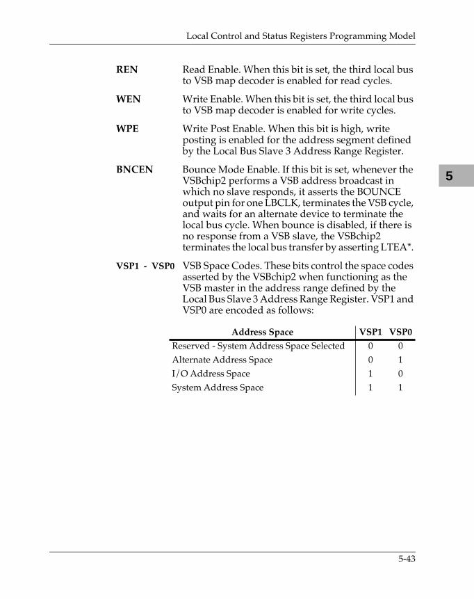
Local Control and Status Registers Programming Model
5
REN Read Enable. When this bit is set, the third local bus to VSB map decoder is enabled for read cycles.
WEN Write Enable. When this bit is set, the third local bus to VSB map decoder is enabled for write cycles.
WPE Write Post Enable. When this bit is high, write posting is enabled for the address segment defined by the Local Bus Slave 3 Address Range Register.
BNCEN Bounce Mode Enable. If this bit is set, whenever the VSBchip2 performs a VSB address broadcast in which no slave responds, it asserts the BOUNCE output pin for one LBCLK, terminates the VSB cycle, and waits for an alternate device to terminate the local bus cycle. When bounce is disabled, if there is no response from a VSB slave, the VSBchip2 terminates the local bus transfer by asserting LTEA*.
VSP1 - VSP0 VSB Space Codes. These bits control the space codes asserted by the VSBchip2 when functioning as the VSB master in the address range defined by the Local Bus Slave 3 Address Range Register. VSP1 and VSP0 are encoded as follows:
Address Space VSP1 VSP0
Reserved - System Address Space Selected 0 0Alternate Address Space 0 1I/O Address Space 1 0System Address Space 1 1
5-43
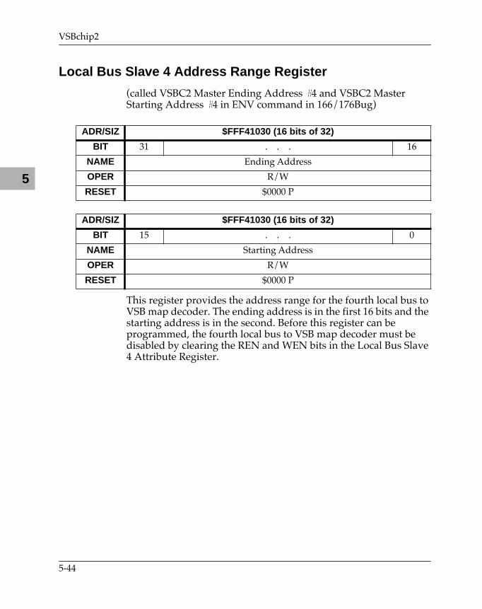
VSBchip2
5
Local Bus Slave 4 Address Range Register
(called VSBC2 Master Ending Address #4 and VSBC2 Master Starting Address #4 in ENV command in 166/176Bug)
This register provides the address range for the fourth local bus to VSB map decoder. The ending address is in the first 16 bits and the starting address is in the second. Before this register can be programmed, the fourth local bus to VSB map decoder must be disabled by clearing the REN and WEN bits in the Local Bus Slave 4 Attribute Register.
ADR/SIZ $FFF41030 (16 bits of 32)
BIT 31 . . . 16
NAME Ending Address
OPER R/W
RESET $0000 P
ADR/SIZ $FFF41030 (16 bits of 32)
BIT 15 . . . 0
NAME Starting Address
OPER R/W
RESET $0000 P
5-44
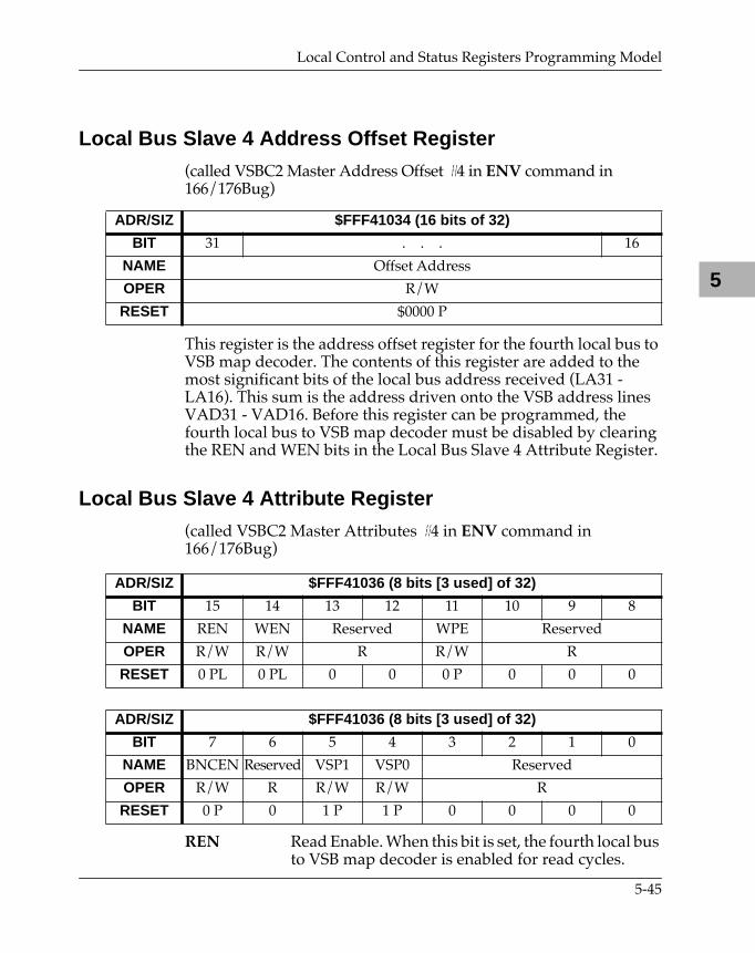
Local Control and Status Registers Programming Model
5
Local Bus Slave 4 Address Offset Register
(called VSBC2 Master Address Offset #4 in ENV command in 166/176Bug)
This register is the address offset register for the fourth local bus to VSB map decoder. The contents of this register are added to the most significant bits of the local bus address received (LA31 - LA16). This sum is the address driven onto the VSB address lines VAD31 - VAD16. Before this register can be programmed, the fourth local bus to VSB map decoder must be disabled by clearing the REN and WEN bits in the Local Bus Slave 4 Attribute Register.
Local Bus Slave 4 Attribute Register
(called VSBC2 Master Attributes #4 in ENV command in 166/176Bug)
REN Read Enable. When this bit is set, the fourth local bus to VSB map decoder is enabled for read cycles.
ADR/SIZ $FFF41034 (16 bits of 32)
BIT 31 . . . 16
NAME Offset Address
OPER R/W
RESET $0000 P
ADR/SIZ $FFF41036 (8 bits [3 used] of 32)
BIT 15 14 13 12 11 10 9 8
NAME REN WEN Reserved WPE Reserved
OPER R/W R/W R R/W R
RESET 0 PL 0 PL 0 0 0 P 0 0 0
ADR/SIZ $FFF41036 (8 bits [3 used] of 32)
BIT 7 6 5 4 3 2 1 0
NAME BNCEN Reserved VSP1 VSP0 Reserved
OPER R/W R R/W R/W R
RESET 0 P 0 1 P 1 P 0 0 0 0
5-45
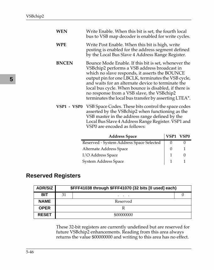
VSBchip2
5
WEN Write Enable. When this bit is set, the fourth local bus to VSB map decoder is enabled for write cycles.
WPE Write Post Enable. When this bit is high, write posting is enabled for the address segment defined by the Local Bus Slave 4 Address Range Register.
BNCEN Bounce Mode Enable. If this bit is set, whenever the VSBchip2 performs a VSB address broadcast in which no slave responds, it asserts the BOUNCE output pin for one LBCLK, terminates the VSB cycle, and waits for an alternate device to terminate the local bus cycle. When bounce is disabled, if there is no response from a VSB slave, the VSBchip2 terminates the local bus transfer by asserting LTEA*.
VSP1 - VSP0 VSB Space Codes. These bits control the space codes asserted by the VSBchip2 when functioning as the VSB master in the address range defined by the Local Bus Slave 4 Address Range Register. VSP1 and VSP0 are encoded as follows:
Reserved Registers
These 32-bit registers are currently undefined but are reserved for future VSBchip2 enhancements. Reading from this area always returns the value $00000000 and writing to this area has no effect.
Address Space VSP1 VSP0
Reserved - System Address Space Selected 0 0Alternate Address Space 0 1I/O Address Space 1 0System Address Space 1 1
ADR/SIZ $FFF41038 through $FFF41070 (32 bits [0 used] each)
BIT 31 . . . 0
NAME Reserved
OPER R
RESET $00000000
5-46
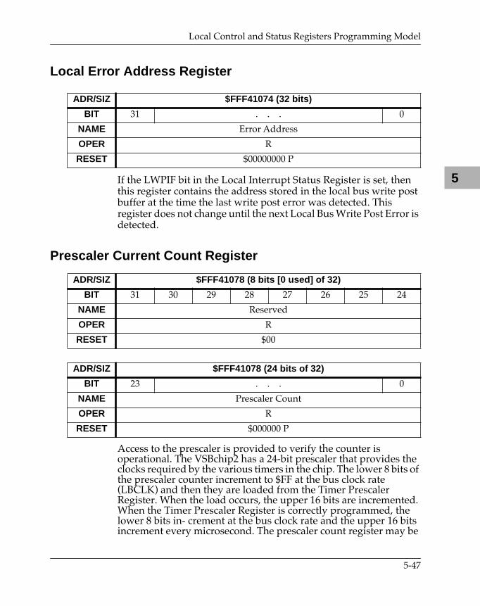
Local Control and Status Registers Programming Model
5
Local Error Address Register
If the LWPIF bit in the Local Interrupt Status Register is set, then this register contains the address stored in the local bus write post buffer at the time the last write post error was detected. This register does not change until the next Local Bus Write Post Error is detected.
Prescaler Current Count Register
Access to the prescaler is provided to verify the counter is operational. The VSBchip2 has a 24-bit prescaler that provides the clocks required by the various timers in the chip. The lower 8 bits of the prescaler counter increment to $FF at the bus clock rate (LBCLK) and then they are loaded from the Timer Prescaler Register. When the load occurs, the upper 16 bits are incremented. When the Timer Prescaler Register is correctly programmed, the lower 8 bits in- crement at the bus clock rate and the upper 16 bits increment every microsecond. The prescaler count register may be
ADR/SIZ $FFF41074 (32 bits)
BIT 31 . . . 0
NAME Error Address
OPER R
RESET $00000000 P
ADR/SIZ $FFF41078 (8 bits [0 used] of 32)
BIT 31 30 29 28 27 26 25 24
NAME Reserved
OPER R
RESET $00
ADR/SIZ $FFF41078 (24 bits of 32)
BIT 23 . . . 0
NAME Prescaler Count
OPER R
RESET $000000 P
5-47
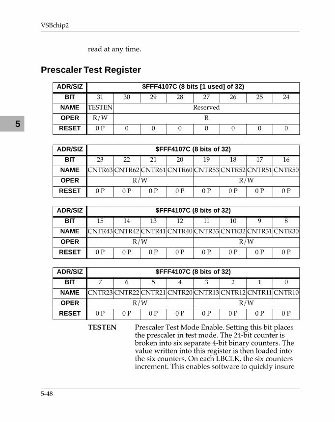
VSBchip2
5
read at any time.
Prescaler Test Register
TESTEN Prescaler Test Mode Enable. Setting this bit places the prescaler in test mode. The 24-bit counter is broken into six separate 4-bit binary counters. The value written into this register is then loaded into the six counters. On each LBCLK, the six counters increment. This enables software to quickly insure
ADR/SIZ $FFF4107C (8 bits [1 used] of 32)
BIT 31 30 29 28 27 26 25 24
NAME TESTEN Reserved
OPER R/W R
RESET 0 P 0 0 0 0 0 0 0
ADR/SIZ $FFF4107C (8 bits of 32)
BIT 23 22 21 20 19 18 17 16
NAME CNTR63 CNTR62 CNTR61 CNTR60 CNTR53 CNTR52 CNTR51 CNTR50
OPER R/W R/W
RESET 0 P 0 P 0 P 0 P 0 P 0 P 0 P 0 P
ADR/SIZ $FFF4107C (8 bits of 32)
BIT 15 14 13 12 11 10 9 8
NAME CNTR43 CNTR42 CNTR41 CNTR40 CNTR33 CNTR32 CNTR31 CNTR30
OPER R/W R/W
RESET 0 P 0 P 0 P 0 P 0 P 0 P 0 P 0 P
ADR/SIZ $FFF4107C (8 bits of 32)
BIT 7 6 5 4 3 2 1 0
NAME CNTR23 CNTR22 CNTR21 CNTR20 CNTR13 CNTR12 CNTR11 CNTR10
OPER R/W R/W
RESET 0 P 0 P 0 P 0 P 0 P 0 P 0 P 0 P
5-48
Local Control and Status Registers Programming Model
5
that segment of the prescaler is operational without waiting 224 clocks.
CNTR13-CNTR10 Counter 1.
CNTR23-CNTR20 Counter 2.
CNTR33-CNTR30 Counter 3.
CNTR43-CNTR40 Counter 4.
CNTR53-CNTR50 Counter 5.
CNTR63-CNTR60 Counter 6.
5-49
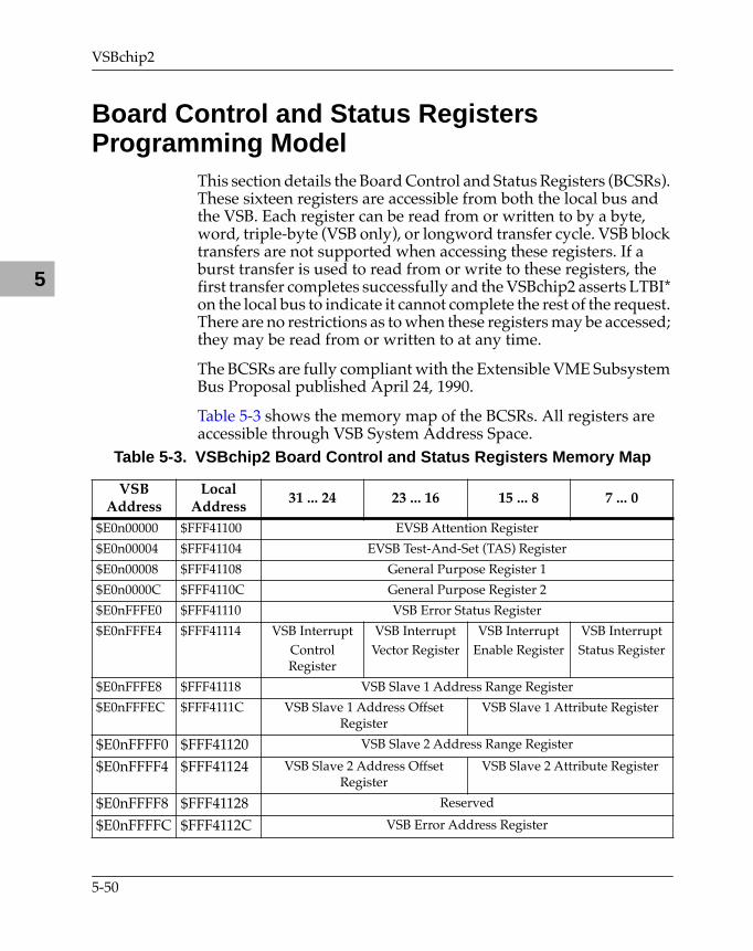
5
VSBchip2
5-50
5VSBchip2
Board Control and Status Registers Programming Model
This section details the Board Control and Status Registers (BCSRs). These sixteen registers are accessible from both the local bus and the VSB. Each register can be read from or written to by a byte, word, triple-byte (VSB only), or longword transfer cycle. VSB block transfers are not supported when accessing these registers. If a burst transfer is used to read from or write to these registers, the first transfer completes successfully and the VSBchip2 asserts LTBI* on the local bus to indicate it cannot complete the rest of the request. There are no restrictions as to when these registers may be accessed; they may be read from or written to at any time.
The BCSRs are fully compliant with the Extensible VME Subsystem Bus Proposal published April 24, 1990.
Table 5-3 shows the memory map of the BCSRs. All registers are accessible through VSB System Address Space.
Table 5-3. VSBchip2 Board Control and Status Registers Memory Map
VSB Address
Local Address
31 ... 24 23 ... 16 15 ... 8 7 ... 0
$E0n00000 $FFF41100 EVSB Attention Register
$E0n00004 $FFF41104 EVSB Test-And-Set (TAS) Register
$E0n00008 $FFF41108 General Purpose Register 1
$E0n0000C $FFF4110C General Purpose Register 2
$E0nFFFE0 $FFF41110 VSB Error Status Register
$E0nFFFE4 $FFF41114 VSB InterruptControl Register
VSB InterruptVector Register
VSB InterruptEnable Register
VSB InterruptStatus Register
$E0nFFFE8 $FFF41118 VSB Slave 1 Address Range Register
$E0nFFFEC $FFF4111C VSB Slave 1 Address Offset Register
VSB Slave 1 Attribute Register
$E0nFFFF0 $FFF41120 VSB Slave 2 Address Range Register
$E0nFFFF4 $FFF41124 VSB Slave 2 Address Offset Register
VSB Slave 2 Attribute Register
$E0nFFFF8 $FFF41128 Reserved
$E0nFFFFC $FFF4112C VSB Error Address Register
Board Control and Status Registers Programming Model
5
Note n = value in SGA2 - SGA0 (Chip Control/Status Register).
Each register is defined by a table with six lines: an ADR/SIZ field, a BIT field, a NAME field, a LOPER field, a VOPER field, and a RESET field. The ADR/SIZ field defines the base addresses of the register and the number of bits defined in the table. The BIT field specifies the function's bit location in the register, and the NAME field is the name of the function. Unused bits are designated 'Reserved' in their NAME field. For these bits, writes have no effect and reads always return a zero. The LOPER field specifies the operations allowed on that bit from the local bus. The VOPER field specifies the operations allowed on that bit from the VSB.
These operations are:
The last field, RESET, specifies the state the bit enters upon application of a reset, and by which reset signal(s) it is affected. The three reset states are 0, 1, or `X' (not affected). The two reset signals are power-up reset (PURST*) signified by the letter `P', and local reset (LBRSTI*) signified by the letter `L'.
R This bit is read only.
R/W This bit is read and write.
R/C This bit is read and clear only.
R/S This bit is read and set only.
5-51
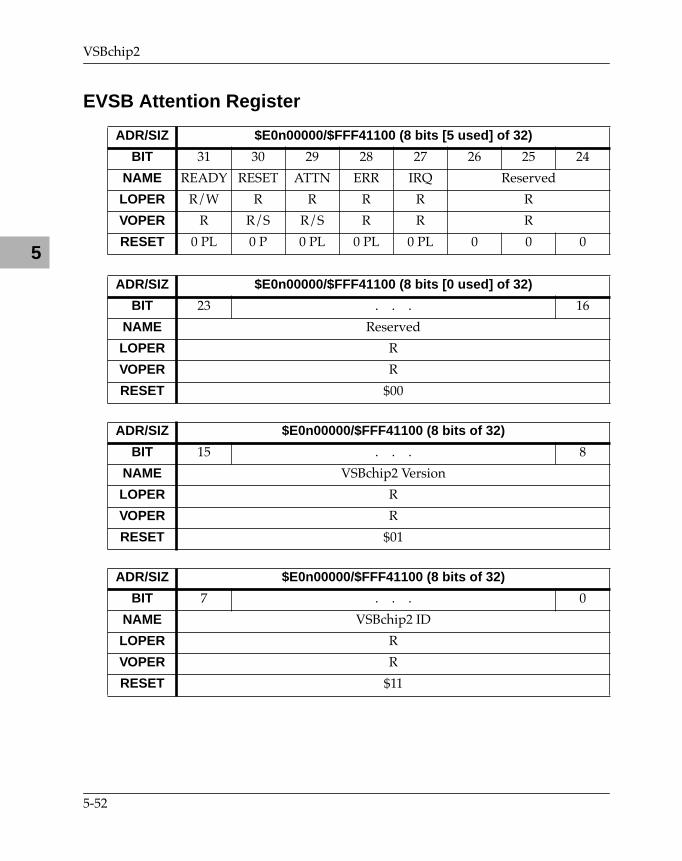
VSBchip2
5
EVSB Attention Register
ADR/SIZ $E0n00000/$FFF41100 (8 bits [5 used] of 32)
BIT 31 30 29 28 27 26 25 24
NAME READY RESET ATTN ERR IRQ Reserved
LOPER R/W R R R R R
VOPER R R/S R/S R R R
RESET 0 PL 0 P 0 PL 0 PL 0 PL 0 0 0
ADR/SIZ $E0n00000/$FFF41100 (8 bits [0 used] of 32)
BIT 23 . . . 16
NAME Reserved
LOPER R
VOPER R
RESET $00
ADR/SIZ $E0n00000/$FFF41100 (8 bits of 32)
BIT 15 . . . 8
NAME VSBchip2 Version
LOPER R
VOPER R
RESET $01
ADR/SIZ $E0n00000/$FFF41100 (8 bits of 32)
BIT 7 . . . 0
NAME VSBchip2 ID
LOPER R
VOPER R
RESET $11
5-52
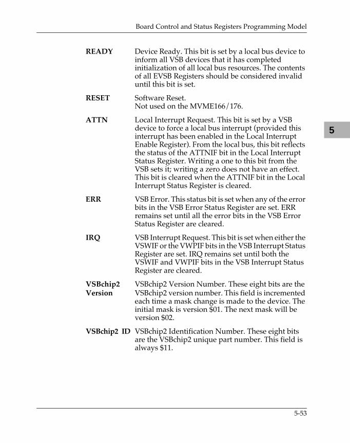
Board Control and Status Registers Programming Model
5
READY Device Ready. This bit is set by a local bus device to inform all VSB devices that it has completed initialization of all local bus resources. The contents of all EVSB Registers should be considered invalid until this bit is set.
RESET Software Reset. Not used on the MVME166/176.
ATTN Local Interrupt Request. This bit is set by a VSB device to force a local bus interrupt (provided this interrupt has been enabled in the Local Interrupt Enable Register). From the local bus, this bit reflects the status of the ATTNIF bit in the Local Interrupt Status Register. Writing a one to this bit from the VSB sets it; writing a zero does not have an effect. This bit is cleared when the ATTNIF bit in the Local Interrupt Status Register is cleared.
ERR VSB Error. This status bit is set when any of the error bits in the VSB Error Status Register are set. ERR remains set until all the error bits in the VSB Error Status Register are cleared.
IRQ VSB Interrupt Request. This bit is set when either the VSWIF or the VWPIF bits in the VSB Interrupt Status Register are set. IRQ remains set until both the VSWIF and VWPIF bits in the VSB Interrupt Status Register are cleared.
VSBchip2 VSBchip2 Version Number. These eight bits are theVersion VSBchip2 version number. This field is incremented
each time a mask change is made to the device. The initial mask is version $01. The next mask will be version $02.
VSBchip2 ID VSBchip2 Identification Number. These eight bits are the VSBchip2 unique part number. This field is always $11.
5-53
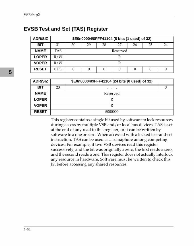
VSBchip2
5
EVSB Test and Set (TAS) Register
This register contains a single bit used by software to lock resources during access by multiple VSB and/or local bus devices. TAS is set at the end of any read to this register, or it can be written by software to a one or zero. When accessed with a locked test-and-set instruction, TAS can be used as a semaphore among competing devices. For example, if two VSB devices read this register successively, and the bit was originally a zero, the first reads a zero, and the second reads a one. This register does not actually interlock any resource in hardware. Software must be written to check this bit before accessing any shared resources.
ADR/SIZ $E0n00004/$FFF41104 (8 bits [1 used] of 32)
BIT 31 30 29 28 27 26 25 24
NAME TAS Reserved
LOPER R/W R
VOPER R/W R
RESET 0 PL 0 0 0 0 0 0 0
ADR/SIZ $E0n00004/$FFF41104 (24 bits [0 used] of 32)
BIT 23 . . . 0
NAME Reserved
LOPER R
VOPER R
RESET $000000
5-54
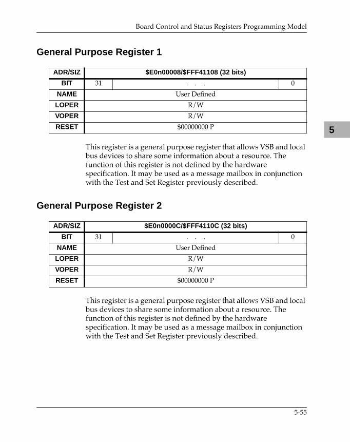
Board Control and Status Registers Programming Model
5
General Purpose Register 1
This register is a general purpose register that allows VSB and local bus devices to share some information about a resource. The function of this register is not defined by the hardware specification. It may be used as a message mailbox in conjunction with the Test and Set Register previously described.
General Purpose Register 2
This register is a general purpose register that allows VSB and local bus devices to share some information about a resource. The function of this register is not defined by the hardware specification. It may be used as a message mailbox in conjunction with the Test and Set Register previously described.
ADR/SIZ $E0n00008/$FFF41108 (32 bits)
BIT 31 . . . 0
NAME User DeÞned
LOPER R/W
VOPER R/W
RESET $00000000 P
ADR/SIZ $E0n0000C/$FFF4110C (32 bits)
BIT 31 . . . 0
NAME User DeÞned
LOPER R/W
VOPER R/W
RESET $00000000 P
5-55
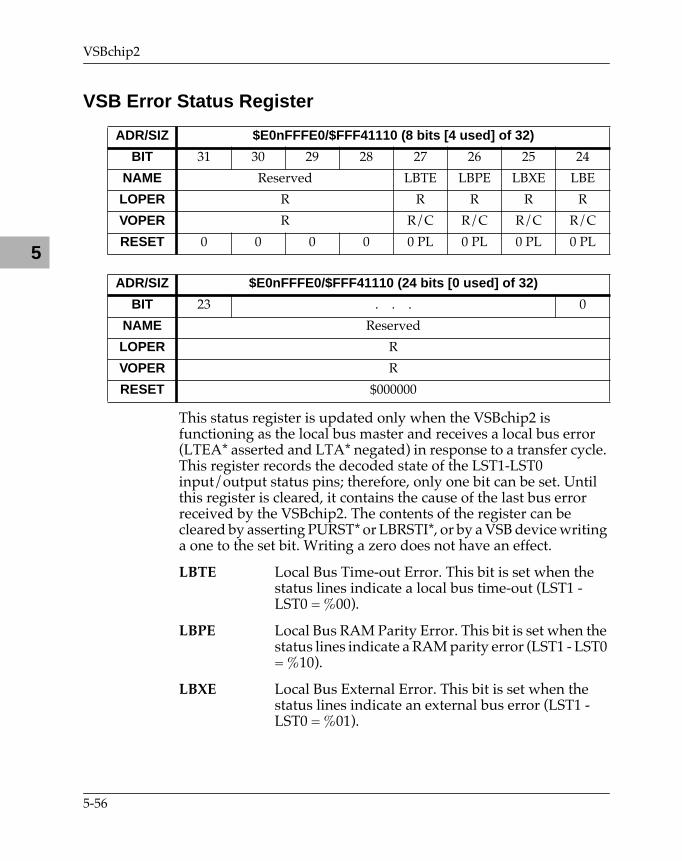
VSBchip2
5
VSB Error Status Register
This status register is updated only when the VSBchip2 is functioning as the local bus master and receives a local bus error (LTEA* asserted and LTA* negated) in response to a transfer cycle. This register records the decoded state of the LST1-LST0 input/output status pins; therefore, only one bit can be set. Until this register is cleared, it contains the cause of the last bus error received by the VSBchip2. The contents of the register can be cleared by asserting PURST* or LBRSTI*, or by a VSB device writing a one to the set bit. Writing a zero does not have an effect.
LBTE Local Bus Time-out Error. This bit is set when the status lines indicate a local bus time-out (LST1 - LST0 = %00).
LBPE Local Bus RAM Parity Error. This bit is set when the status lines indicate a RAM parity error (LST1 - LST0 = %10).
LBXE Local Bus External Error. This bit is set when the status lines indicate an external bus error (LST1 - LST0 = %01).
ADR/SIZ $E0nFFFE0/$FFF41110 (8 bits [4 used] of 32)
BIT 31 30 29 28 27 26 25 24
NAME Reserved LBTE LBPE LBXE LBE
LOPER R R R R R
VOPER R R/C R/C R/C R/C
RESET 0 0 0 0 0 PL 0 PL 0 PL 0 PL
ADR/SIZ $E0nFFFE0/$FFF41110 (24 bits [0 used] of 32)
BIT 23 . . . 0
NAME Reserved
LOPER R
VOPER R
RESET $000000
5-56
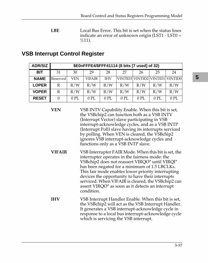
Board Control and Status Registers Programming Model
5
LBE Local Bus Error. This bit is set when the status lines indicate an error of unknown origin (LST1 - LST0 = %11).
VSB Interrupt Control Register
VEN VSB INTV Capability Enable. When this bit is set, the VSBchip2 can function both as a VSB INTV (Interrupt Vector) slave participating in VSB interrupt-acknowledge cycles, and as a VSB INTP (Interrupt Poll) slave having its interrupts serviced by polling. When VEN is cleared, the VSBchip2 ignores VSB interrupt-acknowledge cycles and functions only as a VSB INTP slave.
VIFAIR VSB Interrupter FAIR Mode. When this bit is set, the interrupter operates in the fairness mode: the VSBchip2 does not reassert VIRQO* until VIRQI* has been negated for a minimum of 1.5 LBCLKs. This fair mode enables lower priority interrupting devices the opportunity to have their interrupts serviced. When VIFAIR is cleared, the VSBchip2 can assert VIRQO* as soon as it detects an interrupt condition.
IHV VSB Interrupt Handler Enable. When this bit is set, the VSBchip2 will act as the VSB Interrupt Handler. It generates a VSB interrupt-acknowledge cycle in response to a local bus interrupt-acknowledge cycle which is servicing the VSB interrupt.
ADR/SIZ $E0nFFFE4/$FFF41114 (8 bits [7 used] of 32)
BIT 31 30 29 28 27 26 25 24
NAME Reserved VEN VIFAIR IHV VINTID3 VINTID2 VINTID1 VINTID0
LOPER R R/W R/W R/W R/W R/W R/W R/W
VOPER R R/W R/W R/W R/W R/W R/W R/W
RESET 0 0 PL 0 PL 0 PL 0 PL 0 PL 0 PL 0 PL
5-57
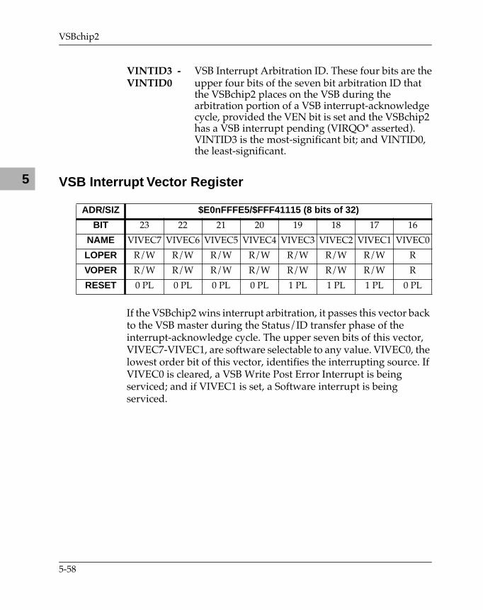
VSBchip2
5
VINTID3 - VSB Interrupt Arbitration ID. These four bits are theVINTID0 upper four bits of the seven bit arbitration ID that
the VSBchip2 places on the VSB during the arbitration portion of a VSB interrupt-acknowledge cycle, provided the VEN bit is set and the VSBchip2 has a VSB interrupt pending (VIRQO* asserted). VINTID3 is the most-significant bit; and VINTID0, the least-significant.
VSB Interrupt Vector Register
If the VSBchip2 wins interrupt arbitration, it passes this vector back to the VSB master during the Status/ID transfer phase of the interrupt-acknowledge cycle. The upper seven bits of this vector, VIVEC7-VIVEC1, are software selectable to any value. VIVEC0, the lowest order bit of this vector, identifies the interrupting source. If VIVEC0 is cleared, a VSB Write Post Error Interrupt is being serviced; and if VIVEC1 is set, a Software interrupt is being serviced.
ADR/SIZ $E0nFFFE5/$FFF41115 (8 bits of 32)
BIT 23 22 21 20 19 18 17 16
NAME VIVEC7 VIVEC6 VIVEC5 VIVEC4 VIVEC3 VIVEC2 VIVEC1 VIVEC0
LOPER R/W R/W R/W R/W R/W R/W R/W R
VOPER R/W R/W R/W R/W R/W R/W R/W R
RESET 0 PL 0 PL 0 PL 0 PL 1 PL 1 PL 1 PL 0 PL
5-58
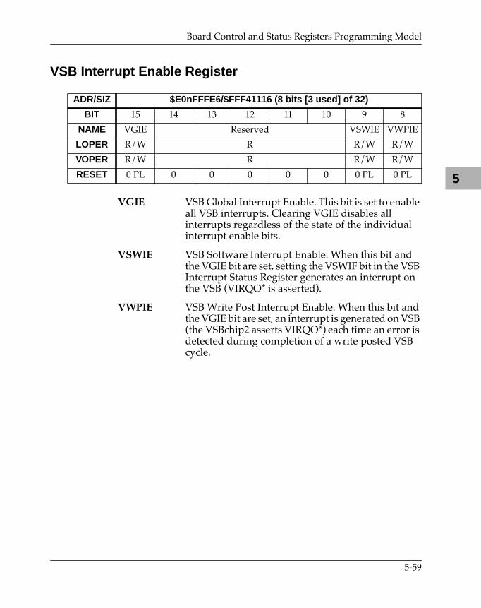
Board Control and Status Registers Programming Model
5
VSB Interrupt Enable Register
VGIE VSB Global Interrupt Enable. This bit is set to enable all VSB interrupts. Clearing VGIE disables all interrupts regardless of the state of the individual interrupt enable bits.
VSWIE VSB Software Interrupt Enable. When this bit and the VGIE bit are set, setting the VSWIF bit in the VSB Interrupt Status Register generates an interrupt on the VSB (VIRQO* is asserted).
VWPIE VSB Write Post Interrupt Enable. When this bit and the VGIE bit are set, an interrupt is generated on VSB (the VSBchip2 asserts VIRQO*) each time an error is detected during completion of a write posted VSB cycle.
ADR/SIZ $E0nFFFE6/$FFF41116 (8 bits [3 used] of 32)
BIT 15 14 13 12 11 10 9 8
NAME VGIE Reserved VSWIE VWPIE
LOPER R/W R R/W R/W
VOPER R/W R R/W R/W
RESET 0 PL 0 0 0 0 0 0 PL 0 PL
5-59
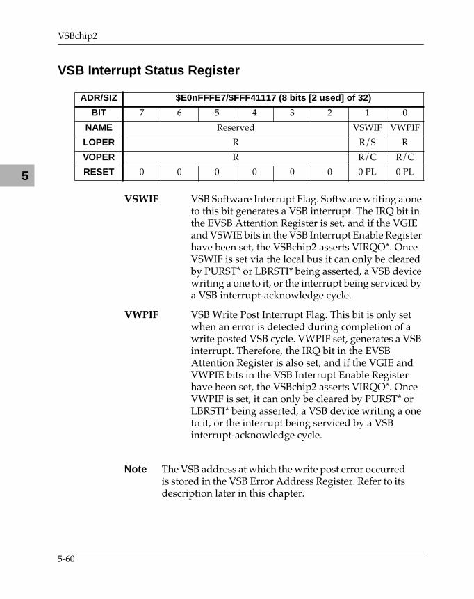
VSBchip2
5
VSB Interrupt Status Register
VSWIF VSB Software Interrupt Flag. Software writing a one to this bit generates a VSB interrupt. The IRQ bit in the EVSB Attention Register is set, and if the VGIE and VSWIE bits in the VSB Interrupt Enable Register have been set, the VSBchip2 asserts VIRQO*. Once VSWIF is set via the local bus it can only be cleared by PURST* or LBRSTI* being asserted, a VSB device writing a one to it, or the interrupt being serviced by a VSB interrupt-acknowledge cycle.
VWPIF VSB Write Post Interrupt Flag. This bit is only set when an error is detected during completion of a write posted VSB cycle. VWPIF set, generates a VSB interrupt. Therefore, the IRQ bit in the EVSB Attention Register is also set, and if the VGIE and VWPIE bits in the VSB Interrupt Enable Register have been set, the VSBchip2 asserts VIRQO*. Once VWPIF is set, it can only be cleared by PURST* or LBRSTI* being asserted, a VSB device writing a one to it, or the interrupt being serviced by a VSB interrupt-acknowledge cycle.
Note The VSB address at which the write post error occurred is stored in the VSB Error Address Register. Refer to its description later in this chapter.
ADR/SIZ $E0nFFFE7/$FFF41117 (8 bits [2 used] of 32)
BIT 7 6 5 4 3 2 1 0
NAME Reserved VSWIF VWPIF
LOPER R R/S R
VOPER R R/C R/C
RESET 0 0 0 0 0 0 0 PL 0 PL
5-60
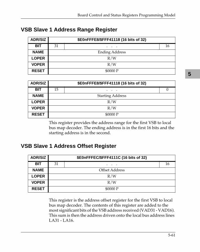
Board Control and Status Registers Programming Model
5
VSB Slave 1 Address Range Register
This register provides the address range for the first VSB to local bus map decoder. The ending address is in the first 16 bits and the starting address is in the second.
VSB Slave 1 Address Offset Register
This register is the address offset register for the first VSB to local bus map decoder. The contents of this register are added to the most significant bits of the VSB address received (VAD31 - VAD16). This sum is then the address driven onto the local bus address lines LA31 - LA16.
ADR/SIZ $E0nFFFE8/$FFF41118 (16 bits of 32)
BIT 31 . . . 16
NAME Ending Address
LOPER R/W
VOPER R/W
RESET $0000 P
ADR/SIZ $E0nFFFE8/$FFF41118 (16 bits of 32)
BIT 15 . . . 0
NAME Starting Address
LOPER R/W
VOPER R/W
RESET $0000 P
ADR/SIZ $E0nFFFEC/$FFF4111C (16 bits of 32)
BIT 31 . . . 16
NAME Offset Address
LOPER R/W
VOPER R/W
RESET $0000 P
5-61
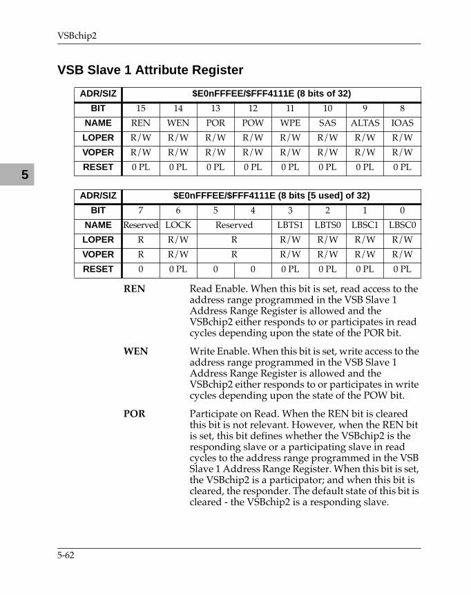
VSBchip2
5
VSB Slave 1 Attribute Register
REN Read Enable. When this bit is set, read access to the address range programmed in the VSB Slave 1 Address Range Register is allowed and the VSBchip2 either responds to or participates in read cycles depending upon the state of the POR bit.
WEN Write Enable. When this bit is set, write access to the address range programmed in the VSB Slave 1 Address Range Register is allowed and the VSBchip2 either responds to or participates in write cycles depending upon the state of the POW bit.
POR Participate on Read. When the REN bit is cleared this bit is not relevant. However, when the REN bit is set, this bit defines whether the VSBchip2 is the responding slave or a participating slave in read cycles to the address range programmed in the VSB Slave 1 Address Range Register. When this bit is set, the VSBchip2 is a participator; and when this bit is cleared, the responder. The default state of this bit is cleared - the VSBchip2 is a responding slave.
ADR/SIZ $E0nFFFEE/$FFF4111E (8 bits of 32)
BIT 15 14 13 12 11 10 9 8
NAME REN WEN POR POW WPE SAS ALTAS IOAS
LOPER R/W R/W R/W R/W R/W R/W R/W R/W
VOPER R/W R/W R/W R/W R/W R/W R/W R/W
RESET 0 PL 0 PL 0 PL 0 PL 0 PL 0 PL 0 PL 0 PL
ADR/SIZ $E0nFFFEE/$FFF4111E (8 bits [5 used] of 32)
BIT 7 6 5 4 3 2 1 0
NAME Reserved LOCK Reserved LBTS1 LBTS0 LBSC1 LBSC0
LOPER R R/W R R/W R/W R/W R/W
VOPER R R/W R R/W R/W R/W R/W
RESET 0 0 PL 0 0 0 PL 0 PL 0 PL 0 PL
5-62

Board Control and Status Registers Programming Model
5
POW Participate on Write. When the WEN bit is cleared this bit is not relevant. However, when the WEN bit is set, this bit defines whether the VSBchip2 is the responding slave or a participating slave in write cycles to the address range programmed in the VSB Slave 1 Address Range Register. When this bit is set, the VSBchip2 is a participator; and when this bit is cleared, the responder. The default state of this bit is cleared - the VSBchip2 is a responding slave.
WPE Write Post Enable. When this bit is set, write posting is enabled for the address range defined by the VSB Slave 1 Address Range Register.
SAS System Address Space. When access to the local bus is permitted (responding or participating capability must be enabled), setting this bit defines the VSB Slave 1 Address Range to be in the VSB System Address Space. This is the default location.
ALTAS Alternate Address Space. When access to the local bus is permitted (responding or participating capability must be enabled), setting this bit defines the VSB Slave 1 Address Range to be in the VSB Alternate Address Space.
IOAS I/O Address Space. When access to the local bus is permitted (responding or participating capability must be enabled), setting this bit defines the VSB Slave 1 Address Range to be in the VSB I/O Address Space.
LOCK Lock Local Bus on Block Transfers. The Lock bit, if set, causes the VSBchip2 local master to assert LBB* on the start of a VSB block transfer. This effectively prevents any other local bus master from taking the bus back, and allows higher speed block transfers. Only when the VSB master removes VPAS*, is the bus released.
This software Lock contrasts with the VSB lock signal (VLOCK*) which may be used to keep the bus locked between VSB transfers as well as within VSB transfers. Using VLOCK* allows an external VSB
5-63
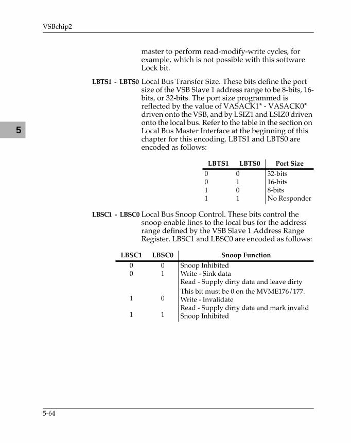
VSBchip2
5
master to perform read-modify-write cycles, for example, which is not possible with this software Lock bit.
LBTS1 - LBTS0 Local Bus Transfer Size. These bits define the port size of the VSB Slave 1 address range to be 8-bits, 16-bits, or 32-bits. The port size programmed is reflected by the value of VASACK1* - VASACK0* driven onto the VSB, and by LSIZ1 and LSIZ0 driven onto the local bus. Refer to the table in the section on Local Bus Master Interface at the beginning of this chapter for this encoding. LBTS1 and LBTS0 are encoded as follows:
LBSC1 - LBSC0 Local Bus Snoop Control. These bits control the snoop enable lines to the local bus for the address range defined by the VSB Slave 1 Address Range Register. LBSC1 and LBSC0 are encoded as follows:
LBTS1 LBTS0 Port Size
0011
0101
32-bits16-bits8-bitsNo Responder
LBSC1 LBSC0 Snoop Function
00
1
1
01
0
1
Snoop InhibitedWrite - Sink dataRead - Supply dirty data and leave dirtyThis bit must be 0 on the MVME176/177.Write - InvalidateRead - Supply dirty data and mark invalidSnoop Inhibited
5-64

Board Control and Status Registers Programming Model
5
VSB Slave 2 Address Range Register
This register provides the address range for the second VSB to local bus map decoder. The ending address is in the first 16 bits and the starting address is in the second.
VSB Slave 2 Address Offset Register
This register is the address offset register for the second VSB to local bus map decoder. The contents of this register are added to the most significant bits of the VSB address received (VAD31 - VAD16). This sum is then the address driven onto the local bus address lines LA31 - LA16.
ADR/SIZ $E0nFFFF0/$FFF41120 (16 bits of 32)
BIT 31 . . . 16
NAME Ending Address
LOPER R/W
VOPER R/W
RESET $0000 P
ADR/SIZ $E0nFFFF0/$FFF41120 (16 bits of 32)
BIT 15 . . . 0
NAME Starting Address
LOPER R/W
VOPER R/W
RESET $0000 P
ADR/SIZ $E0nFFFF4/$FFF41124 (16 bits of 32)
BIT 31 . . . 16
NAME Offset Address
LOPER R/W
VOPER R/W
RESET $0000 P
5-65

VSBchip2
5
VSB Slave 2 Attribute Register
REN Read Enable. When this bit is set, read access to the address range programmed in the VSB Slave 2 Address Range Register is allowed and the VSBchip2 either responds to or participates in read cycles depending upon the state of the POR bit.
WEN Write Enable. When this bit is set, write access to the address range programmed in the VSB Slave 2 Address Range Register is allowed and the VSBchip2 either responds to or participates in write cycles depending upon the state of the POW bit.
POR Participate on Read. When the REN bit is cleared this bit is not relevant. However, when the REN bit is set, this bit defines whether the VSBchip2 is the responding slave or a participating slave in read cycles to the address range programmed in the VSB Slave 2 Address Range Register. When this bit is set, the VSBchip2 is a participator; and when this bit is cleared, the responder. The default state of this bit is cleared - the VSBchip2 is a responding slave.
ADR/SIZ $E0nFFFF6/$FFF41126 (8 bits of 32)
BIT 15 14 13 12 11 10 9 8
NAME REN WEN POR POW WPE SAS ALTAS IOAS
LOPER R/W R/W R/W R/W R/W R/W R/W R/W
VOPER R/W R/W R/W R/W R/W R/W R/W R/W
RESET 0 PL 0 PL 0 PL 0 PL 0 PL 1PL 0 PL 0 PL
ADR/SIZ $E0nFFFF6/$FFF41126 (8 bits [5 used] of 32)
BIT 7 6 5 4 3 2 1 0
NAME Reserved LOCK Reserved LBTS1 LBTS0 LBSC1 LBSC0
LOPER R R/W R R/W R/W R/W R/W
VOPER R R/W R R/W R/W R/W R/W
RESET 0 0 PL 0 0 0 PL 0 PL 0 PL 0 PL
5-66
Board Control and Status Registers Programming Model
5
POW Participate on Write. When the WEN bit is cleared this bit is not relevant. However, when the WEN bit is set, this bit defines whether the VSBchip2 is the responding slave or a participating slave in write cycles to the address range programmed in the VSB Slave 2 Address Range Register. When this bit is set, the VSBchip2 is a participator; and when this bit is cleared, the responder. The default state of this bit is cleared - the VSBchip2 is a responding slave.
WPE Write Post Enable. When this bit is set, write posting is enabled for the address range defined by the VSB Slave 2 Address Range Register.
SAS System Address Space. When access to the local bus is permitted (responding or participating capability must be enabled), setting this bit defines the VSB Slave 2 Address Range to be in the VSB System Address Space. This is the default location.
ALTAS Alternate Address Space. When access to the local bus is permitted (responding or participating capability must be enabled), setting this bit defines the VSB Slave 2 Address Range to be in the VSB Alternate Address Space.
IOAS I/O Address Space. When access to the local bus is permitted (responding or participating capability must be enabled), setting this bit defines the VSB Slave 2 Address Range to be in the VSB I/O Address Space.
LOCK Lock Local Bus on Block Transfers. The Lock bit, if set, causes the VSBchip2 local master to assert LBB* on the start of a VSB block transfer. This effectively prevents any other local bus master from taking the bus back, and allows higher speed block transfers. Only when the VSB master removes VPAS*, is the bus released.
This software Lock contrasts with the VSB lock signal (VLOCK*) which may be used to keep the bus locked between VSB transfers as well as within VSB transfers. Using VLOCK* allows an external VSB
5-67

VSBchip2
5
master to perform read-modify-write cycles, for example, which is not possible with this software Lock bit.
LBTS1 - LBTS0 Local Bus Transfer Size. These bits define the port size of the VSB Slave 2 address range to be 8-bits, 16-bits, or 32-bits. The port size programmed is reflected by the value of VASACK1* - VASACK0* driven onto the VSB, and by LSIZ1 and LSIZ0 driven onto the local bus. Refer to the table in the section on Local Bus Master Interface at the beginning of this chapter for this encoding. LBTS1 and LBTS0 are encoded as follows:
LBSC1 - LBSC0 Local Bus Snoop Control. These bits control the snoop enable lines to the local bus for the address range defined by the VSB Slave 2 Address Range Register. LBSC1 and LBSC0 are encoded as follows:
LBTS1 LBTS0 Port Size
0011
0101
32-bits16-bits8-bitsNo Responder
LBSC1 LBSC0 Snoop Function
00
1
1
01
0
1
Snoop InhibitedWrite - Sink dataRead - Supply dirty data and leave dirtyThis bit must be 0 on the MVME176/177.Write - InvalidateRead - Supply dirty data and mark invalidSnoop Inhibited
5-68
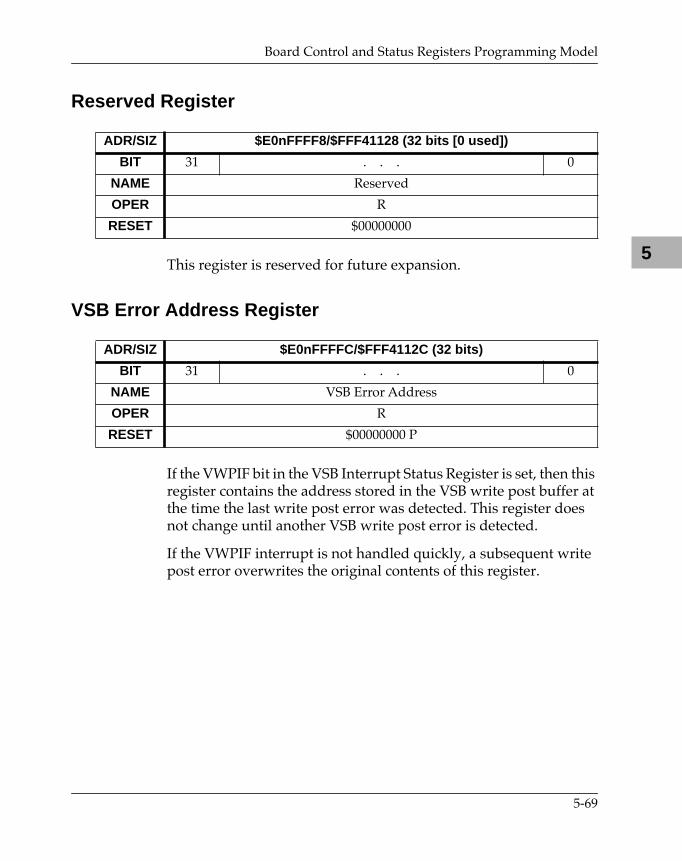
Board Control and Status Registers Programming Model
5
Reserved Register
This register is reserved for future expansion.
VSB Error Address Register
If the VWPIF bit in the VSB Interrupt Status Register is set, then this register contains the address stored in the VSB write post buffer at the time the last write post error was detected. This register does not change until another VSB write post error is detected.
If the VWPIF interrupt is not handled quickly, a subsequent write post error overwrites the original contents of this register.
ADR/SIZ $E0nFFFF8/$FFF41128 (32 bits [0 used])
BIT 31 . . . 0
NAME Reserved
OPER R
RESET $00000000
ADR/SIZ $E0nFFFFC/$FFF4112C (32 bits)
BIT 31 . . . 0
NAME VSB Error Address
OPER R
RESET $00000000 P
5-69
VSBchip2
5
5-70
6
6PCCchip2IntroductionThis chapter defines the peripheral channel controller ASIC which is referred to as the PCCchip2 hereafter. The PCCchip2 is designed to interface an MC68040-compatible local bus (Local Bus) to various peripheral devices.
Summary of Major Features
This section lists the major features of the PCCchip2.
❏ BBRAM interface with dynamic sizing support.
❏ Map decoder for MEMC040 Memory Controller ASIC.
❏ 8-bit parallel I/O port.
❏ Master and slave interface for CD2401 Intelligent Multi-Protocol Peripheral.
❏ Host interface to Intel 82596CA LAN Coprocessor.
❏ Host interface to NCR SCSI I/O Processor.
❏ Two 32-bit tick timers.
❏ Interrupt handler for tick timers and all peripherals:
Ð All interrupts are level-programmable.
Ð All interrupts are maskable.
Ð All interrupts provide a unique vector.
❏ Interrupt Mask Register to help prioritize interrupt requests to the MC88100.
6-1
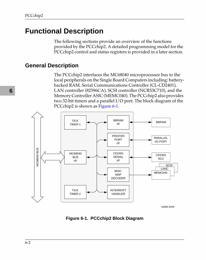
PCCchip2
6
Functional DescriptionThe following sections provide an overview of the functions provided by the PCCchip2. A detailed programming model for the PCCchip2 control and status registers is provided in a later section.
General Description
The PCCchip2 interfaces the MC68040 microprocessor bus to the local peripherals on the Single Board Computers including: battery-backed RAM, Serial Communications Controller (CL-CD2401), LAN controller (82596CA), SCSI controller (NCR53C710), and the Memory Controller ASIC (MEMC040). The PCCchip2 also provides two 32-bit timers and a parallel I/O port. The block diagram of the PCCchip2 is shown as Figure 6-1.
Figure 6-1. PCCchip2 Block Diagram
BBRAM
PARALLELI/O PORT
CD2401SCC
TICKTIMER 1
TICKTIMER 2
INTERRUPTHANDLER
BBRAMI/F
PRINTERPORT
I/F
CD2401SERIAL
I/F
MISC.MAP
DECODER
bd065 9209
SCSI
MEMC040LANC
MC68040BUSI/F
MC
6804
0 B
US
6-2
Functional Description
6
BBRAM Interface
The PCCchip2 provides a read/write interface to the BBRAM by any bus master on the MC68040 bus. The PCCchip2 performs dynamic sizing for accesses to the 8-bit BBRAM to make it appear contiguous. This feature allows code to be executable from the BBRAM. The BBRAM device access time must be no greater than 5 BCLK periods in fast mode or 9 BCLK periods in slow mode. The BBRAM speed option is controlled by a control bit in the General Control Register.
Download ROM Interface (MVME166 Only)
The PCCchip2 provides a read/write interface to the download ROM (DROM) for any master on the MC68040 bus. The PCCchip2 performs dynamic sizing for accesses to the 8-bit DROM to make it appear contiguous. This feature allows code to be executable from the DROM. The DROM device access time must be no greater than 5 BCLK periods in fast mode or 9 BCLK periods in slow mode. The DROM speed option is controlled by a control bit in the General Control Register.
If the DR0 bit is set in the General Control Register, DROM appears at locations $00000000 through $0001FFFF in addition to its normal address range.
DR0 is normally cleared at local or power-up reset. However, if no other device responds to the first memory access on the Local Bus, after reset, the PCCchip2 sets DR0, causing DROM to respond to the memory access. DR0 remains set until software writes a 0 to it. (The PCCchip2 determines that no device is responding to the vector fetch by detecting the lack of TA* or TEA* for 32 BCLK cycles after the assertion of TS*.)
6-3
PCCchip2
6
82596CA LAN Controller Interface
The LAN controller interface is described in the following sections.
MPU Port and MPU Channel Attention
The PCCchip2 allows the Local Bus (MC68040-compatible) bus master to communicate directly with the Intel 82596CA LAN Coprocessor by providing a map decoder and required control and timing logic. Two types of direct access are feasible with the 82596CA: MPU Port and MPU Attention.
MPU Port access enables the MPU to write to an internal, 32-bit 82596CA command register. This allows the MPU to do four things:
1. Write an alternate System Configuration Pointer address.
2. Write an alternative dump area pointer and perform a dump.
3. Execute a software reset.
4. Execute a self-test.
Each Port access must consist of two 16-bit writes: Upper Command Word (two bytes) and Lower Command Word (two bytes). The Upper Command Word (two bytes) is mapped at $FFF46000 and the Lower Command Word (two bytes) is mapped at $FFF46002.
The PCCchip2 only supports (decodes) MPU Port writes. It does not decode MPU Port reads. (Nor does the 82596CA support MPU Port reads.)
MPU Channel Attention access is used to cause the 82596CA to begin executing memory resident Command blocks. To execute an MPU Channel Attention, the Local Bus bus master performs a simple read or write to address $FFF46004.
6-4
Functional Description
6
MC68040-Bus Master Support for 82596CA
The 82596CA has DMA capability with an Intel i486-bus interface. When it is the local bus master, external hardware is needed to convert its bus cycles into MC68040-bus cycles. When the 82596CA has local bus mastership, the PCCchip2 drives the following Local Bus (MC68040-bus) signal lines:
❏ Snoop Control SC1-SC0. (With the value programmed into the LAN Interrupt Control Register.) (Only SC1 is used on the MVME176/177.)
❏ Transfer Types TT1-TT0. (With the value of %00.)
❏ Transfer Modifiers TM2-TM0. (With the value of %101.)
❏ Transfer Acknowledge (TA*) if Transfer Error Acknowledge (TEA*) is detected.
LANC Bus Error
The 82596CA does not provide a way to terminate a bus cycle with an error indication. The interface to the 82596CA on the Single Board Computers provides several ways of processing bus errors that occur while the 82596CA is local bus master. These options are controlled by registers in the VMEchip2 and the PCCchip2.
The GPIO2 signal on the VMEchip2 LCSR (address $FFF40088) controls how the 82596CA interface logic responds to bus errors. If the GPIO2 signal is programmed as an input (reset state) or programmed as an output and set high, bus errors are processed in the following way.
The 82596CA interface logic monitors all bus cycles initiated by the 82596CA, and if a bus error is indicated (TEA* = 0 and TA* = 1), the Back Off signal (BOFF*) to the 82596CA is asserted to keep the 82596CA off the local bus and prevent it from transmitting bad data or corrupting local memory. The LANC Error Status Register in the PCCchip2 is updated and a LANC bus error interrupt is generated
6-5
PCCchip2
6
if it is enabled in the PCCchip2. The Back Off signal remains asserted until the 82596CA is reset via a port reset command. After the 82596CA is reset, pending operations must be restarted.
If the GPIO2 signal is programmed as an output and set low, bus errors are processed in the following way. The 82596CA interface logic monitors all bus cycles initiated by the 82596CA, and if a bus error is indicated (TEA* = 0 and TA* = 1), the interface logic asserts the TA* signal to terminate the bus cycle. The LANC Error Status Register in the PCCchip2 is updated and a LANC bus error interrupt is generated if it is enabled in the PCCchip2. In this case the 82596CA continues to operate and because the cycle was terminated with an error, the 82596CA may transmit bad data or corrupt memory.
LANC Interrupt
When the PCCchip2 detects a high level on the INT signal from the 82596CA, if such interrupts are enabled, it generates an interrupt to the MPU.
If the C040 bit is set, the interrupt request goes to the MPU via the EIPL* pins at the level that is programmed for LANC interrupts in the LANC Interrupt Control Register.
If the C040 bit is cleared, the interrupt goes to the MPU via the INT pin (if the level that is programmed for LANC interrupts in the LANC Interrupt Control Register is higher than the level set in the Interrupt Mask Level Register).
When the MPU acknowledges the LANC interrupt, the PCCchip2 responds with the vector that corresponds to LANC interrupts.
6-6
Functional Description
6
53C710 SCSI Controller Interface
The PCCchip2 provides a map decoder and an interrupt handler for the NCR-53C710 SCSI I/O Processor. The base address for the 53C710 is $FFF47000.
When the PCCchip2 detects low a level on the IRQ* line from the 53C710, if such interrupts are enabled, it generates an interrupt to the MPU.
If the C040 bit is set, the interrupt request goes to the MPU via the EIPL* pins at the level that is programmed for SCSI interrupts in the SCSI Interrupt Control Register.
If the C040 bit is cleared, the interrupt goes to the MPU via the INT pin (if the level that is programmed for SCSI interrupts in the SCSI Interrupt Control Register is higher than the level set in the Interrupt Mask Level Register).
Memory Controller MEMC040 Interface
The PCCchip2 decodes the address for accesses to the memory controller MEMC040. The base address for the MEMC040 is $FFF43000.
Parallel Port Interface
The PCCchip2 provides an 8/16-bit bidirectional parallel port. All eight/sixteen bits of the port must be either inputs or outputs (no individual selection). In addition to the 8/16 bits of data, there are two control pins and five status pins. Each of the status pins can generate an interrupt to the MPU in any of the following programmable conditions: high level, low level, high-to-low transition, or low-to-high transition. This port may be used as a parallel printer port or as a general parallel I/O port.
6-7
PCCchip2
6
When used as a parallel printer port, the five status pins function as: Printer Acknowledge (ACK), Printer Fault (FAULT*), Printer Busy (BSY), Printer Select (SELECT), and Printer Paper Error (PE); while the control pins act as Printer Strobe (STROBE*), and Input Prime (INP*).
The PCCchip2 provides an auto-strobe feature similar to that of the MVME147 PCC. In auto-strobe mode, after a write to the Printer Data Register, the PCCchip2 automatically asserts the STROBE* pin for a selected time specified by the Printer Fast Strobe control bit. In manual mode, the Printer Strobe control bit directly controls the state of the STROBE* pin.
General Purpose I/O Pin
The General Purpose I/O pin can be used as an input pin, as an output pin, or as both. The PCCchip2 has a status bit that reflects the state of the pin. The PCCchip2 also has a control bit that allows it to drive the pin, and another control bit that controls the level that is driven.
The input can be configured to generate an interrupt to the MPU in any of the following programmable conditions: high level, low level, high-to-low transition, or low-to-high transition.
CD2401 SCC Interface
The PCCchip2 provides the required logic to interface the CL-CD2401 (SCC) Intelligent MultiProtocol Peripheral to the MC68040-compatible Local Bus. The interface logic consists of a local master interface, a local slave interface, a CD2401 Host interface, a CD2401 DMA interface, a CD2401 interrupt handler, and a Local Bus requester.
The base address for the CL-CD2401 is $FFF45000. It has 8- and 16-bit registers only. Consequently it does not respond when accessed with a size of 4 bytes (SIZ1,0 = %00) or with a size of 16 bytes (SIZ1,0 = %11).
6-8
Functional Description
6
There are three interrupts sources from the SCC: receive interrupt, transmit interrupt, and modem interrupt. The PCCchip2 provides the ability to individually program the priority level of each of these interrupt sources.
When the C040 bit is set, these interrupts are sent to the MPU via the EIPL* pins (at the programmed level).
When the C040 bit is cleared, they are sent to the MPU via the INT pin. (The INT pin is only asserted if the programmed level of the interrupt source is higher than the level programmed into the Interrupt Mask Level Register.)
There are two interrupt acknowledge modes supported by the PCCchip2 for the SCC: auto vector and direct. In auto vector mode, the PCCchip2 supplies the interrupt vector to the MPU. (No interrupt acknowledge cycle is seen by the CD2401.) In direct mode, the SCC supplies the vector to the MPU. (The PCCchip2 passes the interrupt acknowledge cycle on through to the CD2401. Note that the PCCchip2 drives the CD2401 A7-A0 pins with $01 for modem interrupt acknowledges, $02 for transmit interrupt acknowledges and $03 for receive interrupt acknowledges.) The use of the auto vector mode is not recommended because the CD2401 can supply the vector and the CD2401 requires an interrupt acknowledge cycle.
In order to support polling with the CD2401, the PCCchip2 supports pseudo interrupt acknowledge (PIACK) cycles to the CD2401. (This is required since the CD2401 has no other way of clearing its interrupt requests.) PIACK cycles happen as follows:
1. The MPU waits for an IRQ bit to be set in one of the three SCC interrupt control registers.
2. The Local Bus master starts a normal read cycle to one of the three PIACK registers in the PCCchip2. (The three PIACK registers correspond to modem, transmit, and receive interrupts respectively.)
3. The PCCchip2 upon detecting the start of the read, performs an interrupt acknowledge cycle to the CD2401. (The PCCchip2 drives the CD2401 A7 through A0 pins with a
6-9
PCCchip2
6
value that corresponds to the PIACK register that is being read. If the Modem PIACK Register is being read, then A7 through A0 = $01. If the Transmit PIACK Register is being read, then A7 through A0 = $02. If the Receive PIACK Register is being read, then A7 through A0 = $03.)
4. As the interrupt acknowledge cycle completes, the PCCchip2 places the vector being driven by the CD2401 onto the Local Bus D0 through D8 and D16 through D23 signals. (From the MPU point of view, the status read from the selected PCCchip2 PIACK register is the vector from the CD2401.)
5. The PCCchip2 signals to the local MPU (via TA*) that the read cycle is complete.
Interrupt Prioritizer (MVME187)
When the local MPU is an MC88100, the PCCchip2 provides circuitry to support a seven level, priority, interrupt scheme. This support circuit is enabled and disabled by the C040 bit in the General Control Register.
When the C040 bit is set, the PCCchip2 drives the level of its highest priority internal interrupt request onto the EIPL<2..0>* pins. It is intended that the EIPL pins be combined outside the chip with any external IPL signals and driven externally to the MPU. The priority interrupt scheme is assumed to be provided in the M68000-family MPU when the C040 bit is set.
When the C040 bit is cleared, the PCCchip2 receives the level that is being driven onto the EIPL<2..0>* pins by external devices. It is intended that all external interrupt sources be combined externally onto the incoming EIPL pins, and that the INT pin from the PCCchip2 be synchronized externally then connected to the INT pin on the MC88100. The PCCchip2 combines the incoming EIPL level with its internal interrupt levels and compares that combined level with the level that is programmed into the Mask Register. If the combined internal and external interrupt request levels are
6-10
Functional Description
6
greater than the mask level, the PCCchip2 asserts the INT pin to the MC88100. There are two actions that cause the INT pin to be asserted:
1. The combined internal and external interrupt request level transitions to a level higher than the mask level programmed in the Mask Register.
2. The MPU writes a mask level into the Mask Register that is lower than the current combined internal and external interrupt request level.
Tick Timer
The PCCchip2 includes two 32-bit general purpose tick timers. The tick timers run on a 1MHz clock which is derived from the processor clock by a prescaler.
Each tick timer has a 32-bit counter, a 32-bit compare register, and a clear-on-compare enable bit. The counter is readable and writable at any time. These timers can be used to generate interrupts at various rates or the counters can be read at various times for interval timing. There are two modes of operation for these timers: free-running and clear-on-compare.
In free-running mode, the timers have a resolution of 1 µs and roll over after the count reaches the maximum value $FFFFFFFF. The rollover period for the timers is 71.6 minutes.
When the counter is enabled in the clear-on-compare mode, it increments every 1 µs until the counter value matches the value in the compare register. When a match occurs, the counter is cleared.
When a match occurs, in either mode, an interrupt is sent to the Local Bus interrupter and the overflow counter is incremented. An interrupt to the Local Bus is only generated if the tick timer interrupt is enabled by the Local Bus interrupter. The overflow counter can be cleared by writing a one to the overflow clear bit.
6-11
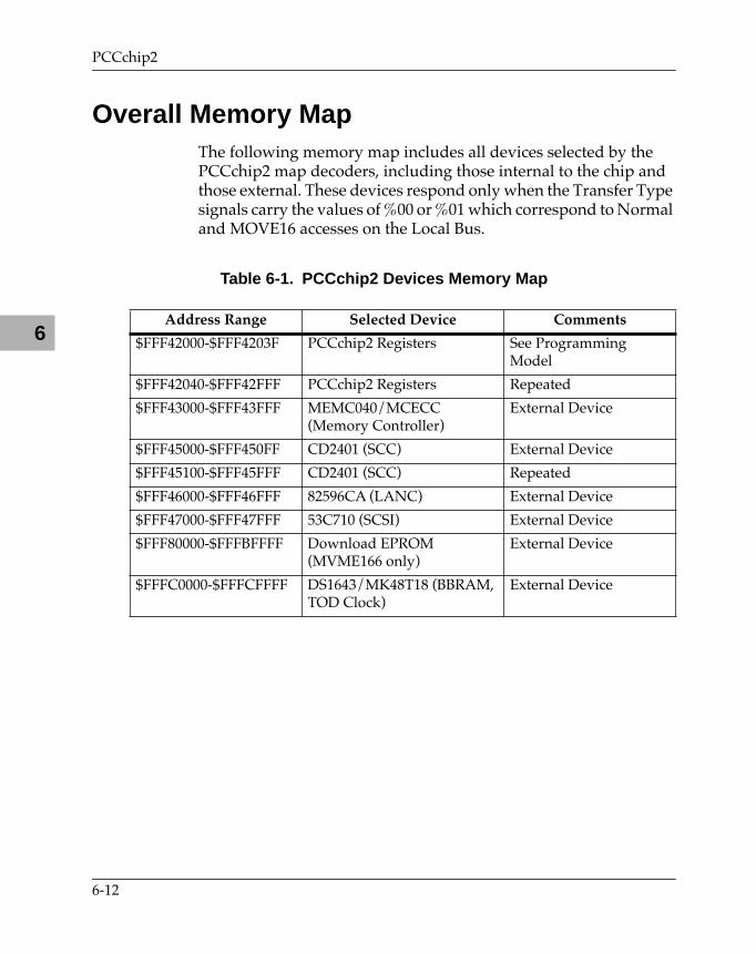
PCCchip2
6
Overall Memory MapThe following memory map includes all devices selected by the PCCchip2 map decoders, including those internal to the chip and those external. These devices respond only when the Transfer Type signals carry the values of %00 or %01 which correspond to Normal and MOVE16 accesses on the Local Bus.
Table 6-1. PCCchip2 Devices Memory Map
Address Range Selected Device Comments
$FFF42000-$FFF4203F PCCchip2 Registers See Programming Model
$FFF42040-$FFF42FFF PCCchip2 Registers Repeated
$FFF43000-$FFF43FFF MEMC040/MCECC (Memory Controller)
External Device
$FFF45000-$FFF450FF CD2401 (SCC) External Device
$FFF45100-$FFF45FFF CD2401 (SCC) Repeated
$FFF46000-$FFF46FFF 82596CA (LANC) External Device
$FFF47000-$FFF47FFF 53C710 (SCSI) External Device
$FFF80000-$FFFBFFFF Download EPROM (MVME166 only)
External Device
$FFFC0000-$FFFCFFFF DS1643/MK48T18 (BBRAM, TOD Clock)
External Device
6-12
Programming Model
6
Programming ModelThis section defines the programming model for the control and status registers (CSR) in the PCCchip2. The base address of the CSR is $FFF42000. The PCCchip2 control and status registers can be accessed as bytes (8 bits), two-bytes (16 bits), or four-bytes(32 bits). The possible operations for each bit in the CSR are as follows:
The possible states of the bits after local and power-up reset are as defined below.
A summary of the PCCchip2 CSR is shown in Table 6-2.
R This bit is a read only status bit.
R/W This bit is readable and writable.
W/AC This bit can be set and it is automatically cleared. This bit can also be read.
C Writing a one to this bit clears this bit or another bit. This bit reads zero.
S Writing a one to this bit sets this bit or another bit. This bit reads zero.
0 This bit is read only. It always reads as 0.
P The bit is affected by power-up reset.
L The bit is affected by local reset.
X The bit is not affected by reset.
V The effect of reset on this bit is variable.
0 The bit is always 0.
1 The bit is always 1.
6-13
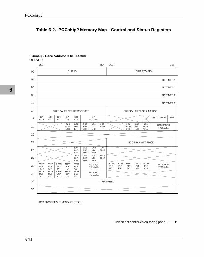
PCCchip2
6
Table 6-2. PCCchip2 Memory Map - Control and Status Registers
This sheet continues on facing page.
PRTRFLT
PLTY
PRTRFLTE/L*
PRTRFLTINT
PRTRFLTIEN
PRTRFLT
ICLR
PRTR FAULTIRQ LEVEL
PRTRACKPLTY
PRTRACKE/L*
PRTRACKINT
PRTRACKIEN
PRTRACKICLR
SCCRTRYERR
PCCchip2 Base Address = $FFF42000OFFSET:
00
04
08
0C
10
14
18
1C
20
24
28
2C
30
34
38
3C
PRTR ACKIRQ LEVEL
GPIPLTY
D16D23D24D31
CHIP ID CHIP REVISION
TIC TIMER 1
TIC TIMER 1
TIC TIMER 2
TIC TIMER 2
PRESCALER COUNT REGISTER PRESCALER CLOCK ADJUST
GPIE/L*
GPIINT
GPIIEN
GPIICLR
GPIIRQ LEVEL
GPI GPOE GPO
SCCPARERR
SCCEXTERR
SCCLTOERR
SCCSCLR
SCCMDMERR
SCCMDMIEN
SCCMDMAVEC
SCC MODEMIRQ LEVEL
SCC TRANSMIT PIACK
LANPARERR
LANEXTERR
LANLTOERR
LANSCLR
SCSIPARERR
SCSIEXTERR
SCSILTOERR
SCSISCLR
PRTRBSYPLTY
PRTRBSYE/L*
PRTRBSYINT
PRTRBSYIEN
PRTRBSYICLR
PRTR BSYIRQ LEVEL
CHIP SPEED
SCC PROVIDES ITS OWN VECTORS
6-14
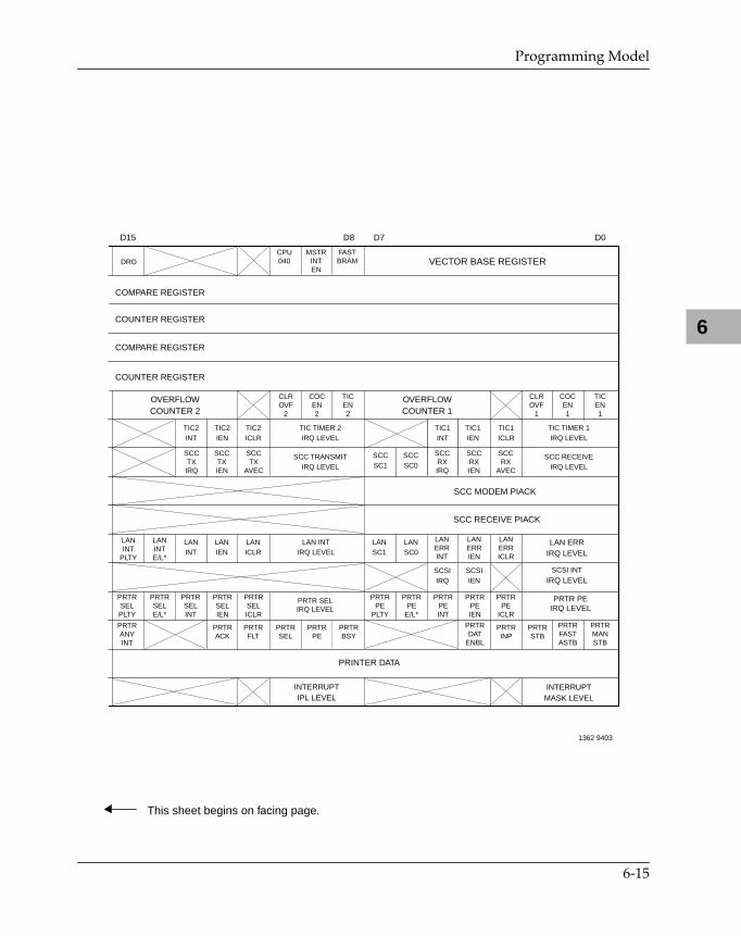
Programming Model
6
This sheet begins on facing page.
INTERRUPTMASK LEVEL
INTERRUPTIPL LEVEL
TIC TIMER 2IRQ LEVEL
SCC TRANSMITIRQ LEVEL
CLROVF
1
COCEN1
TICEN1
CPU040
MSTRINTEN
FASTBRAM
OVERFLOWCOUNTER 2
TIC TIMER 1IRQ LEVEL
SCC RECEIVEIRQ LEVEL
SCC RECEIVE PIACK
LANINT
PLTY
TIC2INT
CLROVF
2
D15 D7D8 D0
VECTOR BASE REGISTERDRO
COMPARE REGISTER
COUNTER REGISTER
COMPARE REGISTER
COUNTER REGISTER
OVERFLOWCOUNTER 1
COCEN2
TICEN2
TIC2IEN
TIC2ICLR
TIC1INT
TIC1IEN
TIC1ICLR
SCCTXIRQ
SCCTXIEN
SCCTX
AVEC
SCCSC1
SCCSC0
SCCRXIRQ
SCCRXIEN
SCCRX
AVEC
SCC MODEM PIACK
LANINTE/L*
LANINT
LANIEN
LANICLR
LAN INTIRQ LEVEL
PRTRSELPLTY
PRTRSELE/L*
PRTRSELINT
PRTRSELIEN
PRTRSELICLR
PRTRANYINT
PRTRACK
PRTRFLT
PRTRSEL
PRTRPE
PRTRBSY
PRTR SELIRQ LEVEL
PRINTER DATA
LANSC1
LANSC0
LANERRINT
LANERRIEN
LANERRICLR
LAN ERRIRQ LEVEL
SCSIIRQ
SCSIIEN
SCSI INT
IRQ LEVEL
PRTR PEIRQ LEVEL
PRTRPE
PLTY
PRTRPE
E/L*
PRTRPEINT
PRTRPEIEN
PRTRPE
ICLR
PRTRDAT
ENBL
PRTRINP
PRTRSTB
PRTRFASTASTB
PRTRMANSTB
1362 9403
6-15
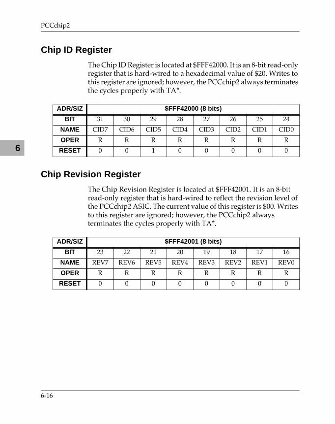
PCCchip2
6
Chip ID Register
The Chip ID Register is located at $FFF42000. It is an 8-bit read-only register that is hard-wired to a hexadecimal value of $20. Writes to this register are ignored; however, the PCCchip2 always terminates the cycles properly with TA*.
Chip Revision Register
The Chip Revision Register is located at $FFF42001. It is an 8-bit read-only register that is hard-wired to reflect the revision level of the PCCchip2 ASIC. The current value of this register is $00. Writes to this register are ignored; however, the PCCchip2 always terminates the cycles properly with TA*.
ADR/SIZ $FFF42000 (8 bits)
BIT 31 30 29 28 27 26 25 24
NAME CID7 CID6 CID5 CID4 CID3 CID2 CID1 CID0
OPER R R R R R R R R
RESET 0 0 1 0 0 0 0 0
ADR/SIZ $FFF42001 (8 bits)
BIT 23 22 21 20 19 18 17 16
NAME REV7 REV6 REV5 REV4 REV3 REV2 REV1 REV0
OPER R R R R R R R R
RESET 0 0 0 0 0 0 0 0
6-16
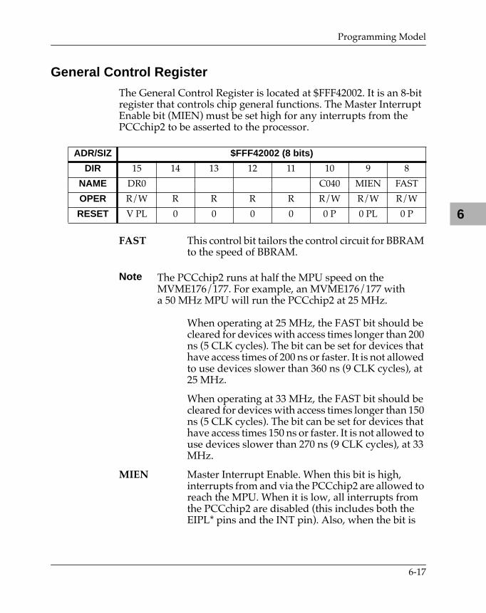
Programming Model
6
General Control Register
The General Control Register is located at $FFF42002. It is an 8-bit register that controls chip general functions. The Master Interrupt Enable bit (MIEN) must be set high for any interrupts from the PCCchip2 to be asserted to the processor.
FAST This control bit tailors the control circuit for BBRAM to the speed of BBRAM.
Note The PCCchip2 runs at half the MPU speed on the MVME176/177. For example, an MVME176/177 with a 50 MHz MPU will run the PCCchip2 at 25 MHz.
When operating at 25 MHz, the FAST bit should be cleared for devices with access times longer than 200 ns (5 CLK cycles). The bit can be set for devices that have access times of 200 ns or faster. It is not allowed to use devices slower than 360 ns (9 CLK cycles), at 25 MHz.
When operating at 33 MHz, the FAST bit should be cleared for devices with access times longer than 150 ns (5 CLK cycles). The bit can be set for devices that have access times 150 ns or faster. It is not allowed to use devices slower than 270 ns (9 CLK cycles), at 33 MHz.
MIEN Master Interrupt Enable. When this bit is high, interrupts from and via the PCCchip2 are allowed to reach the MPU. When it is low, all interrupts from the PCCchip2 are disabled (this includes both the EIPL* pins and the INT pin). Also, when the bit is
ADR/SIZ $FFF42002 (8 bits)
DIR 15 14 13 12 11 10 9 8
NAME DR0 C040 MIEN FAST
OPER R/W R R R R R/W R/W R/W
RESET V PL 0 0 0 0 0 P 0 PL 0 P
6-17
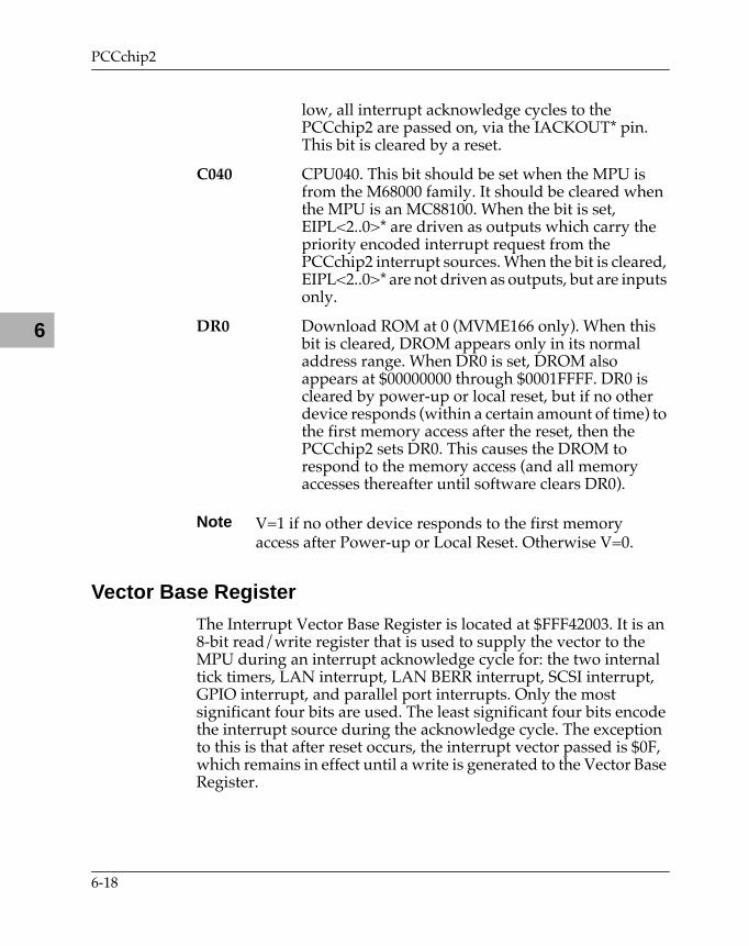
PCCchip2
6
low, all interrupt acknowledge cycles to the PCCchip2 are passed on, via the IACKOUT* pin. This bit is cleared by a reset.
C040 CPU040. This bit should be set when the MPU is from the M68000 family. It should be cleared when the MPU is an MC88100. When the bit is set, EIPL<2..0>* are driven as outputs which carry the priority encoded interrupt request from the PCCchip2 interrupt sources. When the bit is cleared, EIPL<2..0>* are not driven as outputs, but are inputs only.
DR0 Download ROM at 0 (MVME166 only). When this bit is cleared, DROM appears only in its normal address range. When DR0 is set, DROM also appears at $00000000 through $0001FFFF. DR0 is cleared by power-up or local reset, but if no other device responds (within a certain amount of time) to the first memory access after the reset, then the PCCchip2 sets DR0. This causes the DROM to respond to the memory access (and all memory accesses thereafter until software clears DR0).
Note V=1 if no other device responds to the first memory access after Power-up or Local Reset. Otherwise V=0.
Vector Base Register
The Interrupt Vector Base Register is located at $FFF42003. It is an 8-bit read/write register that is used to supply the vector to the MPU during an interrupt acknowledge cycle for: the two internal tick timers, LAN interrupt, LAN BERR interrupt, SCSI interrupt, GPIO interrupt, and parallel port interrupts. Only the most significant four bits are used. The least significant four bits encode the interrupt source during the acknowledge cycle. The exception to this is that after reset occurs, the interrupt vector passed is $0F, which remains in effect until a write is generated to the Vector Base Register.
6-18
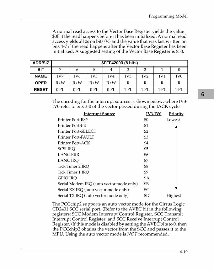
Programming Model
6
A normal read access to the Vector Base Register yields the value $0F if the read happens before it has been initialized. A normal read access yields all 0s on bits 0-3 and the value that was last written on bits 4-7 if the read happens after the Vector Base Register has been initialized. A suggested setting of the Vector Base Register is $50.
The encoding for the interrupt sources is shown below, where IV3-IV0 refer to bits 3-0 of the vector passed during the IACK cycle:
The PCCchip2 supports an auto vector mode for the Cirrus Logic CD2401 SCC serial port. (Refer to the AVEC bit in the following registers: SCC Modem Interrupt Control Register, SCC Transmit Interrupt Control Register, and SCC Receive Interrupt Control Register.) If this mode is disabled by setting the AVEC bits to 0, then the PCCchip2 obtains the vector from the SCC and passes it to the MPU. Using the auto vector mode is NOT recommended.
ADR/SIZ $FFF42003 (8 bits)
BIT 7 6 5 4 3 2 1 0
NAME IV7 IV6 IV5 IV4 IV3 IV2 IV1 IV0
OPER R/W R/W R/W R/W R R R R
RESET 0 PL 0 PL 0 PL 0 PL 1 PL 1 PL 1 PL 1 PL
Interrupt Source IV3-IV0 PriorityPrinter Port-BSY $0 LowestPrinter Port-PE $1Printer Port-SELECT $2Printer Port-FAULT $3Printer Port-ACK $4SCSI IRQ $5LANC ERR $6LANC IRQ $7Tick Timer 2 IRQ $8Tick Timer 1 IRQ $9GPIO IRQ $ASerial Modem IRQ (auto vector mode only) $BSerial RX IRQ (auto vector mode only) $CSerial TX IRQ (auto vector mode only) $D Highest
6-19
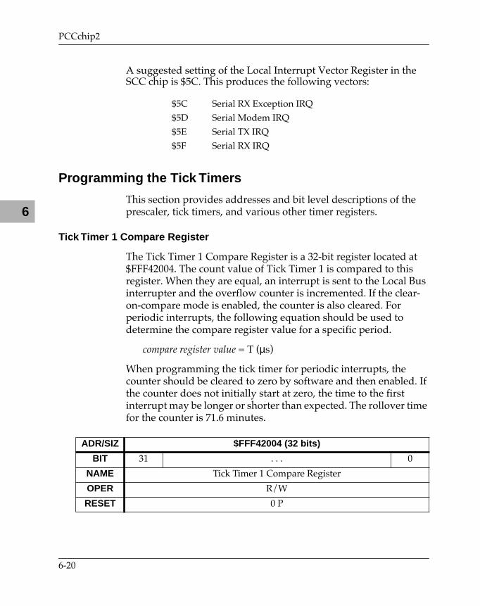
PCCchip2
6
A suggested setting of the Local Interrupt Vector Register in the SCC chip is $5C. This produces the following vectors:
Programming the Tick Timers
This section provides addresses and bit level descriptions of the prescaler, tick timers, and various other timer registers.
Tick Timer 1 Compare Register
The Tick Timer 1 Compare Register is a 32-bit register located at $FFF42004. The count value of Tick Timer 1 is compared to this register. When they are equal, an interrupt is sent to the Local Bus interrupter and the overflow counter is incremented. If the clear-on-compare mode is enabled, the counter is also cleared. For periodic interrupts, the following equation should be used to determine the compare register value for a specific period.
compare register value = T (µs)
When programming the tick timer for periodic interrupts, the counter should be cleared to zero by software and then enabled. If the counter does not initially start at zero, the time to the first interrupt may be longer or shorter than expected. The rollover time for the counter is 71.6 minutes.
$5C Serial RX Exception IRQ$5D Serial Modem IRQ$5E Serial TX IRQ$5F Serial RX IRQ
ADR/SIZ $FFF42004 (32 bits)
BIT 31 . . . 0
NAME Tick Timer 1 Compare Register
OPER R/W
RESET 0 P
6-20
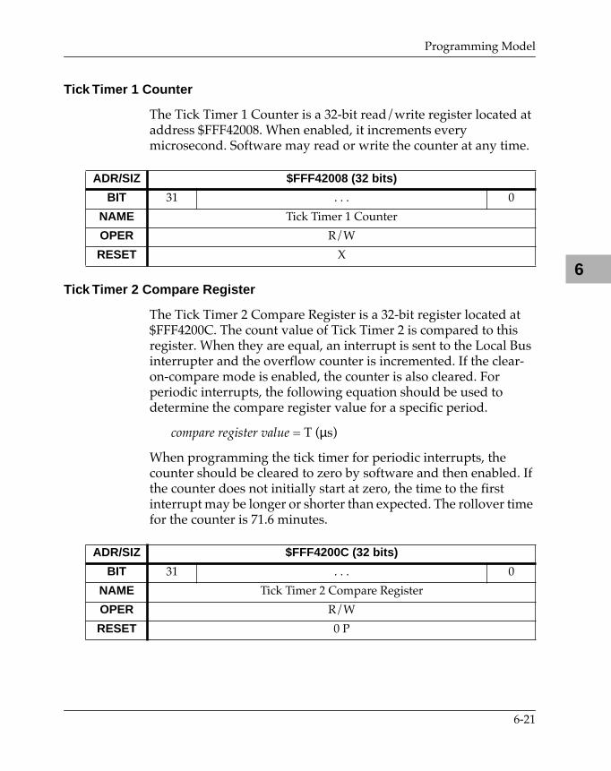
Programming Model
6
Tick Timer 1 Counter
The Tick Timer 1 Counter is a 32-bit read/write register located at address $FFF42008. When enabled, it increments every microsecond. Software may read or write the counter at any time.
Tick Timer 2 Compare Register
The Tick Timer 2 Compare Register is a 32-bit register located at $FFF4200C. The count value of Tick Timer 2 is compared to this register. When they are equal, an interrupt is sent to the Local Bus interrupter and the overflow counter is incremented. If the clear-on-compare mode is enabled, the counter is also cleared. For periodic interrupts, the following equation should be used to determine the compare register value for a specific period.
compare register value = T (µs)
When programming the tick timer for periodic interrupts, the counter should be cleared to zero by software and then enabled. If the counter does not initially start at zero, the time to the first interrupt may be longer or shorter than expected. The rollover time for the counter is 71.6 minutes.
ADR/SIZ $FFF42008 (32 bits)
BIT 31 . . . 0
NAME Tick Timer 1 Counter
OPER R/W
RESET X
ADR/SIZ $FFF4200C (32 bits)
BIT 31 . . . 0
NAME Tick Timer 2 Compare Register
OPER R/W
RESET 0 P
6-21
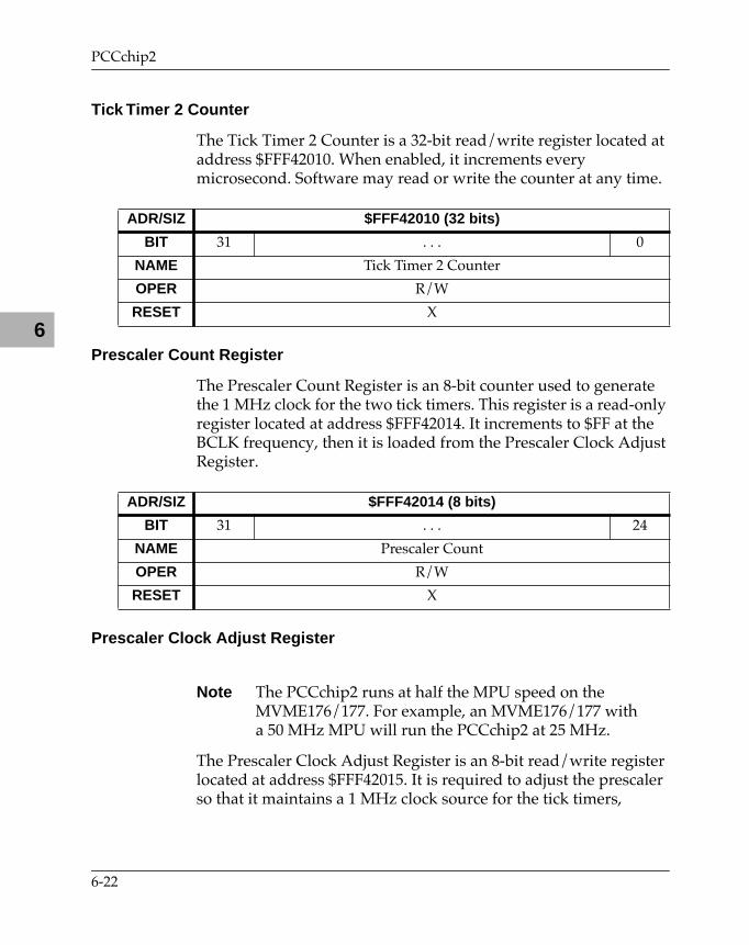
PCCchip2
6
Tick Timer 2 Counter
The Tick Timer 2 Counter is a 32-bit read/write register located at address $FFF42010. When enabled, it increments every microsecond. Software may read or write the counter at any time.
Prescaler Count Register
The Prescaler Count Register is an 8-bit counter used to generate the 1 MHz clock for the two tick timers. This register is a read-only register located at address $FFF42014. It increments to $FF at the BCLK frequency, then it is loaded from the Prescaler Clock Adjust Register.
Prescaler Clock Adjust Register
Note The PCCchip2 runs at half the MPU speed on the MVME176/177. For example, an MVME176/177 with a 50 MHz MPU will run the PCCchip2 at 25 MHz.
The Prescaler Clock Adjust Register is an 8-bit read/write register located at address $FFF42015. It is required to adjust the prescaler so that it maintains a 1 MHz clock source for the tick timers,
ADR/SIZ $FFF42010 (32 bits)
BIT 31 . . . 0
NAME Tick Timer 2 Counter
OPER R/W
RESET X
ADR/SIZ $FFF42014 (8 bits)
BIT 31 . . . 24
NAME Prescaler Count
OPER R/W
RESET X
6-22
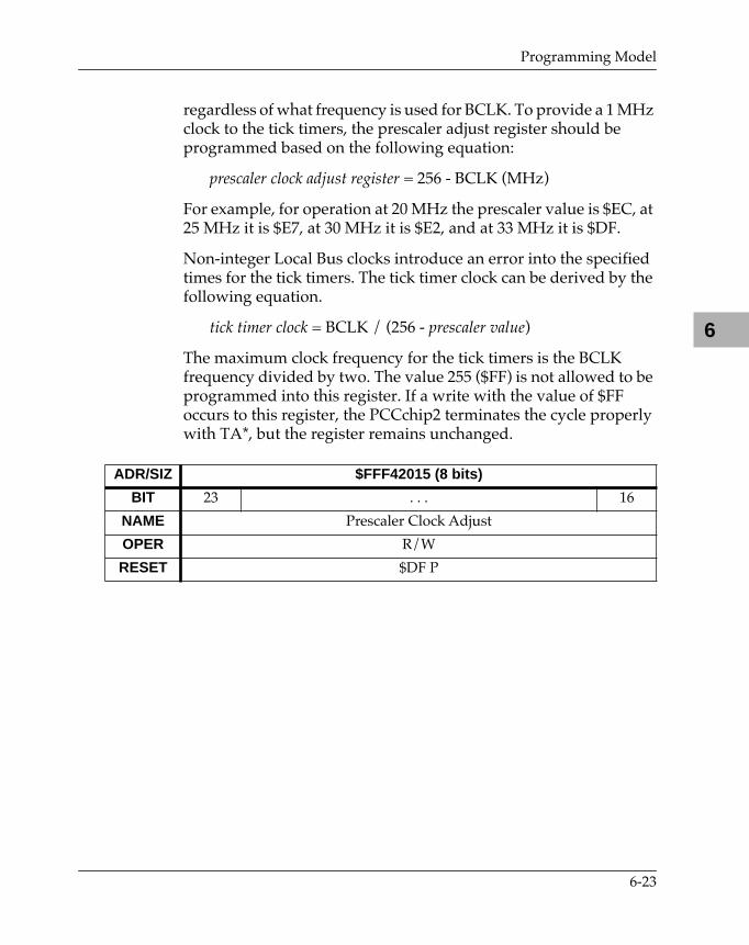
Programming Model
6
regardless of what frequency is used for BCLK. To provide a 1 MHz clock to the tick timers, the prescaler adjust register should be programmed based on the following equation:
prescaler clock adjust register = 256 - BCLK (MHz)
For example, for operation at 20 MHz the prescaler value is $EC, at 25 MHz it is $E7, at 30 MHz it is $E2, and at 33 MHz it is $DF.
Non-integer Local Bus clocks introduce an error into the specified times for the tick timers. The tick timer clock can be derived by the following equation.
tick timer clock = BCLK / (256 - prescaler value)
The maximum clock frequency for the tick timers is the BCLK frequency divided by two. The value 255 ($FF) is not allowed to be programmed into this register. If a write with the value of $FF occurs to this register, the PCCchip2 terminates the cycle properly with TA*, but the register remains unchanged.
ADR/SIZ $FFF42015 (8 bits)
BIT 23 . . . 16
NAME Prescaler Clock Adjust
OPER R/W
RESET $DF P
6-23
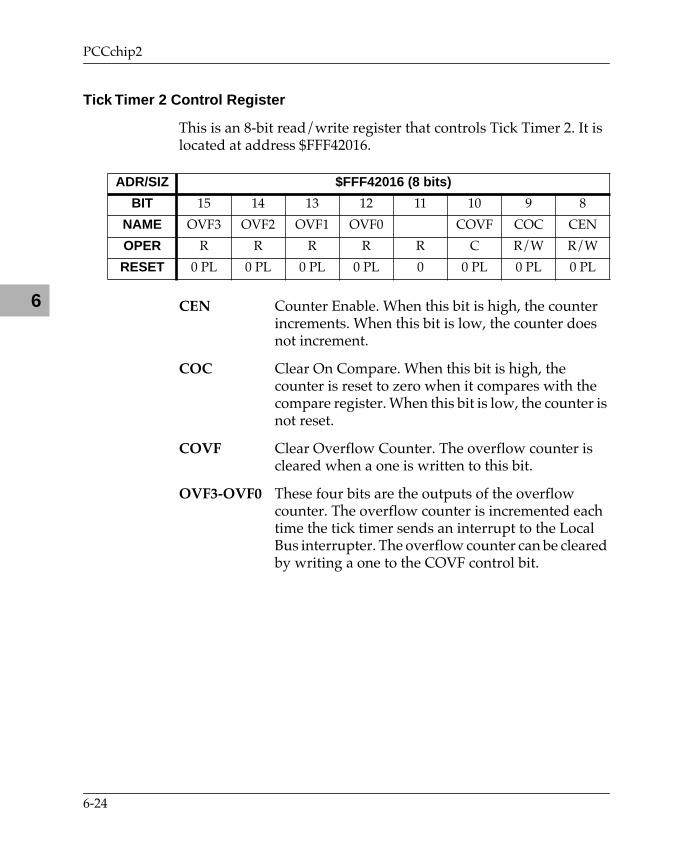
PCCchip2
6
Tick Timer 2 Control Register
This is an 8-bit read/write register that controls Tick Timer 2. It is located at address $FFF42016.
CEN Counter Enable. When this bit is high, the counter increments. When this bit is low, the counter does not increment.
COC Clear On Compare. When this bit is high, the counter is reset to zero when it compares with the compare register. When this bit is low, the counter is not reset.
COVF Clear Overflow Counter. The overflow counter is cleared when a one is written to this bit.
OVF3-OVF0 These four bits are the outputs of the overflow counter. The overflow counter is incremented each time the tick timer sends an interrupt to the Local Bus interrupter. The overflow counter can be cleared by writing a one to the COVF control bit.
ADR/SIZ $FFF42016 (8 bits)
BIT 15 14 13 12 11 10 9 8
NAME OVF3 OVF2 OVF1 OVF0 COVF COC CEN
OPER R R R R R C R/W R/W
RESET 0 PL 0 PL 0 PL 0 PL 0 0 PL 0 PL 0 PL
6-24
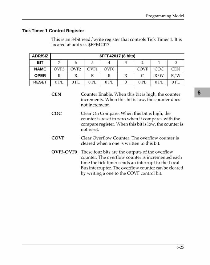
Programming Model
6
Tick Timer 1 Control Register
This is an 8-bit read/write register that controls Tick Timer 1. It is located at address $FFF42017.
CEN Counter Enable. When this bit is high, the counter increments. When this bit is low, the counter does not increment.
COC Clear On Compare. When this bit is high, the counter is reset to zero when it compares with the compare register. When this bit is low, the counter is not reset.
COVF Clear Overflow Counter. The overflow counter is cleared when a one is written to this bit.
OVF3-OVF0 These four bits are the outputs of the overflow counter. The overflow counter is incremented each time the tick timer sends an interrupt to the Local Bus interrupter. The overflow counter can be cleared by writing a one to the COVF control bit.
ADR/SIZ $FFF42017 (8 bits)
BIT 7 6 5 4 3 2 1 0
NAME OVF3 OVF2 OVF1 OVF0 COVF COC CEN
OPER R R R R R C R/W R/W
RESET 0 PL 0 PL 0 PL 0 PL 0 0 PL 0 PL 0 PL
6-25
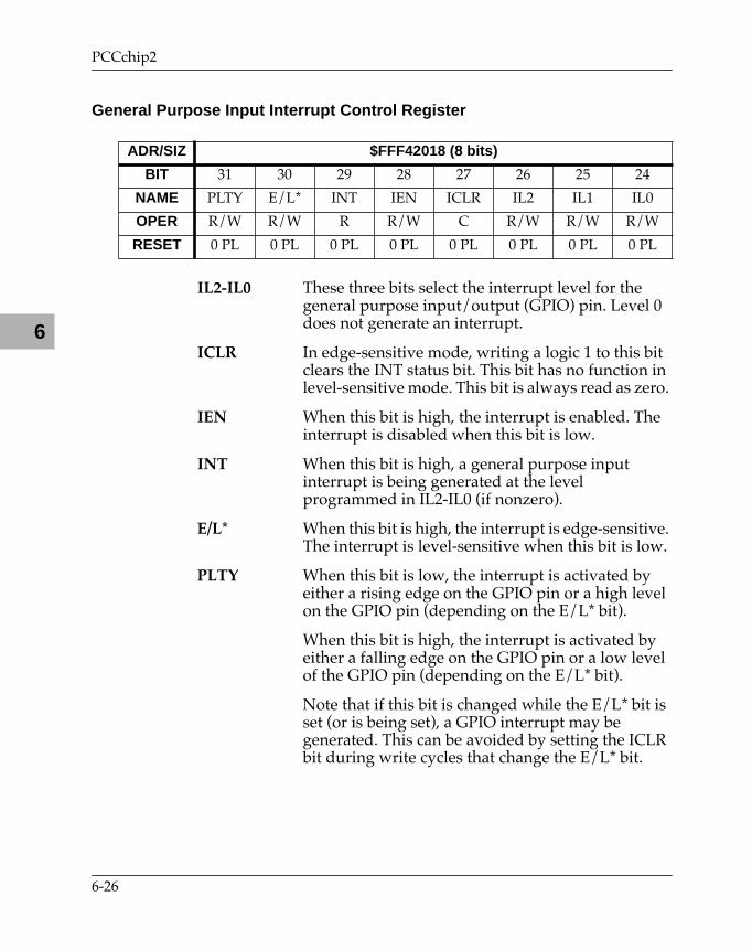
PCCchip2
6
General Purpose Input Interrupt Control Register
IL2-IL0 These three bits select the interrupt level for the general purpose input/output (GPIO) pin. Level 0 does not generate an interrupt.
ICLR In edge-sensitive mode, writing a logic 1 to this bit clears the INT status bit. This bit has no function in level-sensitive mode. This bit is always read as zero.
IEN When this bit is high, the interrupt is enabled. The interrupt is disabled when this bit is low.
INT When this bit is high, a general purpose input interrupt is being generated at the level programmed in IL2-IL0 (if nonzero).
E/L* When this bit is high, the interrupt is edge-sensitive. The interrupt is level-sensitive when this bit is low.
PLTY When this bit is low, the interrupt is activated by either a rising edge on the GPIO pin or a high level on the GPIO pin (depending on the E/L* bit).
When this bit is high, the interrupt is activated by either a falling edge on the GPIO pin or a low level of the GPIO pin (depending on the E/L* bit).
Note that if this bit is changed while the E/L* bit is set (or is being set), a GPIO interrupt may be generated. This can be avoided by setting the ICLR bit during write cycles that change the E/L* bit.
ADR/SIZ $FFF42018 (8 bits)
BIT 31 30 29 28 27 26 25 24
NAME PLTY E/L* INT IEN ICLR IL2 IL1 IL0
OPER R/W R/W R R/W C R/W R/W R/W
RESET 0 PL 0 PL 0 PL 0 PL 0 PL 0 PL 0 PL 0 PL
6-26
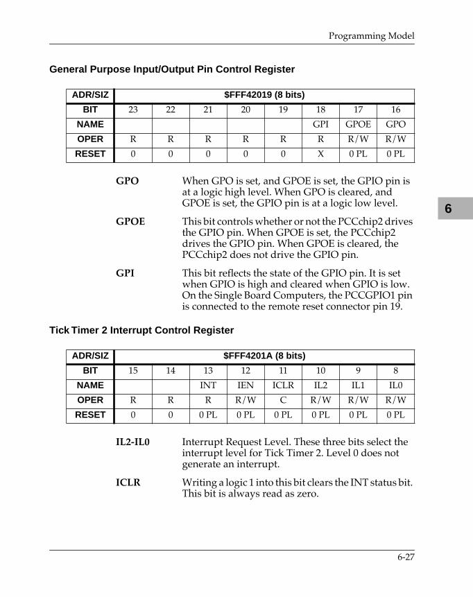
Programming Model
6
General Purpose Input/Output Pin Control Register
GPO When GPO is set, and GPOE is set, the GPIO pin is at a logic high level. When GPO is cleared, and GPOE is set, the GPIO pin is at a logic low level.
GPOE This bit controls whether or not the PCCchip2 drives the GPIO pin. When GPOE is set, the PCCchip2 drives the GPIO pin. When GPOE is cleared, the PCCchip2 does not drive the GPIO pin.
GPI This bit reflects the state of the GPIO pin. It is set when GPIO is high and cleared when GPIO is low. On the Single Board Computers, the PCCGPIO1 pin is connected to the remote reset connector pin 19.
Tick Timer 2 Interrupt Control Register
IL2-IL0 Interrupt Request Level. These three bits select the interrupt level for Tick Timer 2. Level 0 does not generate an interrupt.
ICLR Writing a logic 1 into this bit clears the INT status bit. This bit is always read as zero.
ADR/SIZ $FFF42019 (8 bits)
BIT 23 22 21 20 19 18 17 16
NAME GPI GPOE GPO
OPER R R R R R R R/W R/W
RESET 0 0 0 0 0 X 0 PL 0 PL
ADR/SIZ $FFF4201A (8 bits)
BIT 15 14 13 12 11 10 9 8
NAME INT IEN ICLR IL2 IL1 IL0
OPER R R R R/W C R/W R/W R/W
RESET 0 0 0 PL 0 PL 0 PL 0 PL 0 PL 0 PL
6-27
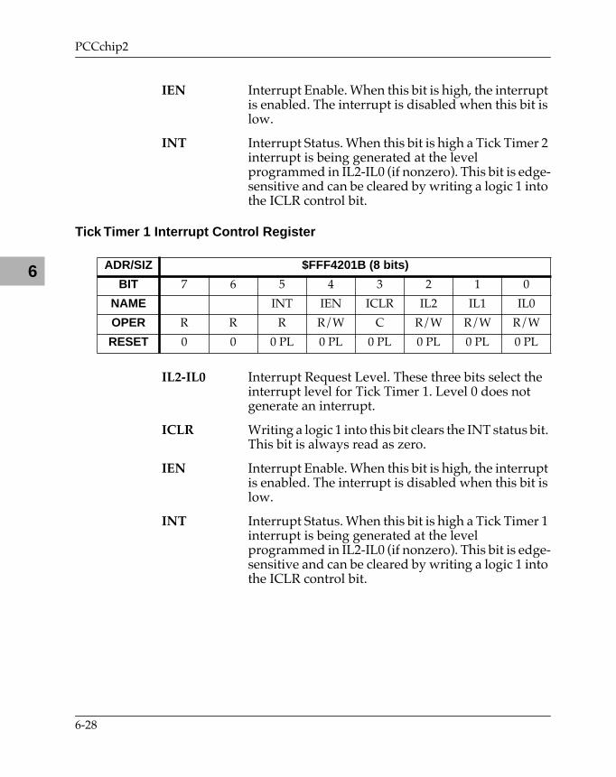
PCCchip2
6
IEN Interrupt Enable. When this bit is high, the interrupt is enabled. The interrupt is disabled when this bit is low.
INT Interrupt Status. When this bit is high a Tick Timer 2 interrupt is being generated at the level programmed in IL2-IL0 (if nonzero). This bit is edge-sensitive and can be cleared by writing a logic 1 into the ICLR control bit.
Tick Timer 1 Interrupt Control Register
IL2-IL0 Interrupt Request Level. These three bits select the interrupt level for Tick Timer 1. Level 0 does not generate an interrupt.
ICLR Writing a logic 1 into this bit clears the INT status bit. This bit is always read as zero.
IEN Interrupt Enable. When this bit is high, the interrupt is enabled. The interrupt is disabled when this bit is low.
INT Interrupt Status. When this bit is high a Tick Timer 1 interrupt is being generated at the level programmed in IL2-IL0 (if nonzero). This bit is edge-sensitive and can be cleared by writing a logic 1 into the ICLR control bit.
ADR/SIZ $FFF4201B (8 bits)
BIT 7 6 5 4 3 2 1 0
NAME INT IEN ICLR IL2 IL1 IL0
OPER R R R R/W C R/W R/W R/W
RESET 0 0 0 PL 0 PL 0 PL 0 PL 0 PL 0 PL
6-28
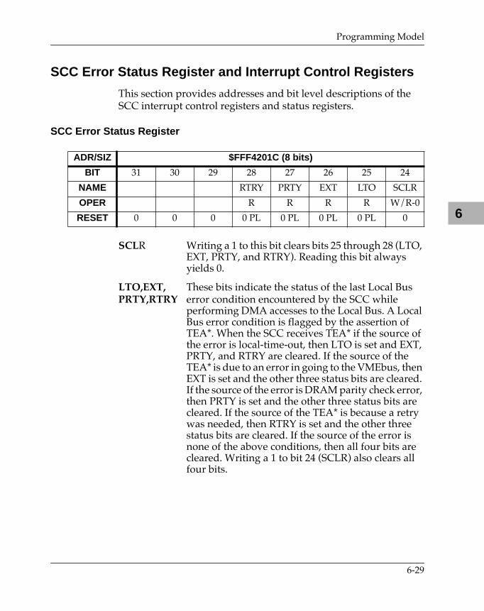
Programming Model
6
SCC Error Status Register and Interrupt Control Registers
This section provides addresses and bit level descriptions of the SCC interrupt control registers and status registers.
SCC Error Status Register
SCLR Writing a 1 to this bit clears bits 25 through 28 (LTO, EXT, PRTY, and RTRY). Reading this bit always yields 0.
LTO,EXT, These bits indicate the status of the last Local BusPRTY,RTRY error condition encountered by the SCC while
performing DMA accesses to the Local Bus. A Local Bus error condition is flagged by the assertion of TEA*. When the SCC receives TEA* if the source of the error is local-time-out, then LTO is set and EXT, PRTY, and RTRY are cleared. If the source of the TEA* is due to an error in going to the VMEbus, then EXT is set and the other three status bits are cleared. If the source of the error is DRAM parity check error, then PRTY is set and the other three status bits are cleared. If the source of the TEA* is because a retry was needed, then RTRY is set and the other three status bits are cleared. If the source of the error is none of the above conditions, then all four bits are cleared. Writing a 1 to bit 24 (SCLR) also clears all four bits.
ADR/SIZ $FFF4201C (8 bits)
BIT 31 30 29 28 27 26 25 24
NAME RTRY PRTY EXT LTO SCLR
OPER R R R R W/R-0
RESET 0 0 0 0 PL 0 PL 0 PL 0 PL 0
6-29
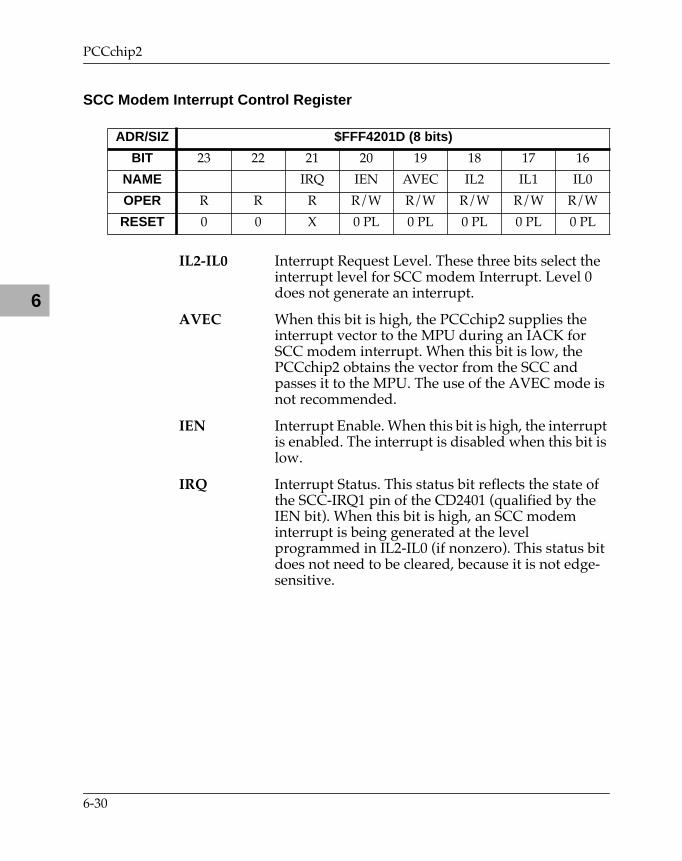
PCCchip2
6
SCC Modem Interrupt Control Register
IL2-IL0 Interrupt Request Level. These three bits select the interrupt level for SCC modem Interrupt. Level 0 does not generate an interrupt.
AVEC When this bit is high, the PCCchip2 supplies the interrupt vector to the MPU during an IACK for SCC modem interrupt. When this bit is low, the PCCchip2 obtains the vector from the SCC and passes it to the MPU. The use of the AVEC mode is not recommended.
IEN Interrupt Enable. When this bit is high, the interrupt is enabled. The interrupt is disabled when this bit is low.
IRQ Interrupt Status. This status bit reflects the state of the SCC-IRQ1 pin of the CD2401 (qualified by the IEN bit). When this bit is high, an SCC modem interrupt is being generated at the level programmed in IL2-IL0 (if nonzero). This status bit does not need to be cleared, because it is not edge-sensitive.
ADR/SIZ $FFF4201D (8 bits)
BIT 23 22 21 20 19 18 17 16
NAME IRQ IEN AVEC IL2 IL1 IL0
OPER R R R R/W R/W R/W R/W R/W
RESET 0 0 X 0 PL 0 PL 0 PL 0 PL 0 PL
6-30
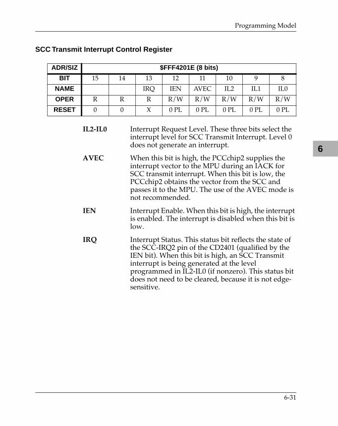
Programming Model
6
SCC Transmit Interrupt Control Register
IL2-IL0 Interrupt Request Level. These three bits select the interrupt level for SCC Transmit Interrupt. Level 0 does not generate an interrupt.
AVEC When this bit is high, the PCCchip2 supplies the interrupt vector to the MPU during an IACK for SCC transmit interrupt. When this bit is low, the PCCchip2 obtains the vector from the SCC and passes it to the MPU. The use of the AVEC mode is not recommended.
IEN Interrupt Enable. When this bit is high, the interrupt is enabled. The interrupt is disabled when this bit is low.
IRQ Interrupt Status. This status bit reflects the state of the SCC-IRQ2 pin of the CD2401 (qualified by the IEN bit). When this bit is high, an SCC Transmit interrupt is being generated at the level programmed in IL2-IL0 (if nonzero). This status bit does not need to be cleared, because it is not edge-sensitive.
ADR/SIZ $FFF4201E (8 bits)
BIT 15 14 13 12 11 10 9 8
NAME IRQ IEN AVEC IL2 IL1 IL0
OPER R R R R/W R/W R/W R/W R/W
RESET 0 0 X 0 PL 0 PL 0 PL 0 PL 0 PL
6-31
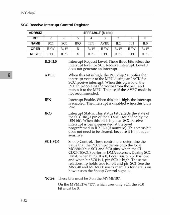
PCCchip2
6
SCC Receive Interrupt Control Register
IL2-IL0 Interrupt Request Level. These three bits select the interrupt level for SCC Receive Interrupt. Level 0 does not generate an interrupt.
AVEC When this bit is high, the PCCchip2 supplies the interrupt vector to the MPU during an IACK for SCC receive interrupt. When this bit is low, the PCCchip2 obtains the vector from the SCC and passes it to the MPU. The use of the AVEC mode is not recommended.
IEN Interrupt Enable. When this bit is high, the interrupt is enabled. The interrupt is disabled when this bit is low.
IRQ Interrupt Status. This status bit reflects the state of the SCC-IRQ3 pin of the CD2401 (qualified by the IEN bit). When this bit is high, an SCC receive interrupt is being generated at the level programmed in IL2-IL0 (if nonzero). This status bit does not need to be cleared, because it is not edge-sensitive.
SC1-SC0 Snoop Control. These control bits determine the value that the PCCchip2 drives onto the local MC68040 bus SC1 and SC0 pins, when the CL-CD2401(SCC) performs DMA accesses. During SCC DMA, when bit SC0 is 0, Local Bus pin SC0 is low, and when bit SC0 is 1, pin SC0 is high. The same relationship holds true for bit and pin SC1. See the M68040 and MC68060 user's manuals for details on how it uses the Snoop Control signals.
Notes These bits must be 0 on the MVME187.
On the MVME176/177, which uses only SC1, the SC0 bit must be 0.
ADR/SIZ $FFF4201F (8 bits)
BIT 7 6 5 4 3 2 1 0
NAME SC1 SC0 IRQ IEN AVEC IL2 IL1 IL0
OPER R/W R/W R R/W R/W R/W R/W R/W
RESET 0 PL 0 PL X 0 PL 0 PL 0 PL 0 PL 0 PL
6-32

Programming Model
6
Modem PIACK Register
The Modem PIACK Register is used to execute modem pseudo interrupt acknowledge cycles to the CD2401.
When the Local Bus master initiates a read cycle to this register, the PCCchip2 executes an interrupt acknowledge cycle to the CD2401 with A7-A0 = $01. (Note that the PILR1 register in the CD2401 should be set to the same value ($01) for the interrupt acknowledge cycle to operate properly.)
To finish the local read cycle, the PCCchip2 drives the vector received from the CD2401 onto the local data bus, and asserts TA*. Reads to this register are termed pseudo interrupt acknowledge cycles because they are normal read cycles on the Local Bus side but they are interrupt acknowledge cycles on the CD2401 side of the PCCchip2. They are necessary to support polled mode operation with the CD2401.
Note If this register is read when an interrupt is not present, the interrupt acknowledge cycle times out with a TEA if the Local Bus timer is enabled.
MIV7-MIV0 Modem interrupt vector bits 7-0 reflect the modem interrupt vector driven by the CD2401 to the PCCchip2 during a pseudo interrupt acknowledge cycle.
ADR/SIZ $FFF42023 (8 bits)
BIT 7 6 5 4 3 2 1 0
NAME MIV7 MIV6 MIV5 MIV4 MIV3 MIV2 MIV1 MIV0
OPER R R R R R R R R
RESET X X X X X X X X
6-33
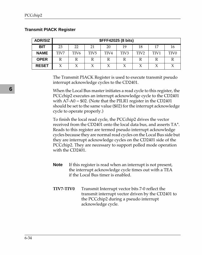
PCCchip2
6
Transmit PIACK Register
The Transmit PIACK Register is used to execute transmit pseudo interrupt acknowledge cycles to the CD2401.
When the Local Bus master initiates a read cycle to this register, the PCCchip2 executes an interrupt acknowledge cycle to the CD2401 with A7-A0 = $02. (Note that the PILR1 register in the CD2401 should be set to the same value ($02) for the interrupt acknowledge cycle to operate properly.)
To finish the local read cycle, the PCCchip2 drives the vector received from the CD2401 onto the local data bus, and asserts TA*. Reads to this register are termed pseudo interrupt acknowledge cycles because they are normal read cycles on the Local Bus side but they are interrupt acknowledge cycles on the CD2401 side of the PCCchip2. They are necessary to support polled mode operation with the CD2401.
Note If this register is read when an interrupt is not present, the interrupt acknowledge cycle times out with a TEA if the Local Bus timer is enabled.
TIV7-TIV0 Transmit Interrupt vector bits 7-0 reflect the transmit interrupt vector driven by the CD2401 to the PCCchip2 during a pseudo interrupt acknowledge cycle.
ADR/SIZ $FFF42025 (8 bits)
BIT 23 22 21 20 19 18 17 16
NAME TIV7 TIV6 TIV5 TIV4 TIV3 TIV2 TIV1 TIV0
OPER R R R R R R R R
RESET X X X X X X X X
6-34
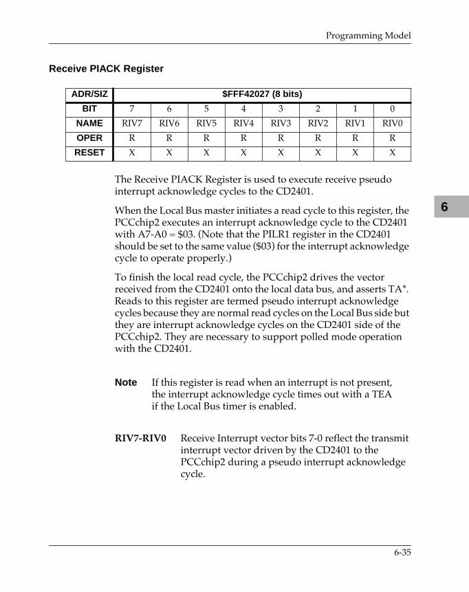
Programming Model
6
Receive PIACK Register
The Receive PIACK Register is used to execute receive pseudo interrupt acknowledge cycles to the CD2401.
When the Local Bus master initiates a read cycle to this register, the PCCchip2 executes an interrupt acknowledge cycle to the CD2401 with A7-A0 = $03. (Note that the PILR1 register in the CD2401 should be set to the same value ($03) for the interrupt acknowledge cycle to operate properly.)
To finish the local read cycle, the PCCchip2 drives the vector received from the CD2401 onto the local data bus, and asserts TA*. Reads to this register are termed pseudo interrupt acknowledge cycles because they are normal read cycles on the Local Bus side but they are interrupt acknowledge cycles on the CD2401 side of the PCCchip2. They are necessary to support polled mode operation with the CD2401.
Note If this register is read when an interrupt is not present, the interrupt acknowledge cycle times out with a TEA if the Local Bus timer is enabled.
RIV7-RIV0 Receive Interrupt vector bits 7-0 reflect the transmit interrupt vector driven by the CD2401 to the PCCchip2 during a pseudo interrupt acknowledge cycle.
ADR/SIZ $FFF42027 (8 bits)
BIT 7 6 5 4 3 2 1 0
NAME RIV7 RIV6 RIV5 RIV4 RIV3 RIV2 RIV1 RIV0
OPER R R R R R R R R
RESET X X X X X X X X
6-35
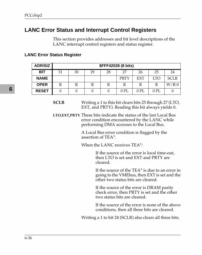
PCCchip2
6
LANC Error Status and Interrupt Control Registers
This section provides addresses and bit level descriptions of the LANC interrupt control registers and status register.
LANC Error Status Register
SCLR Writing a 1 to this bit clears bits 25 through 27 (LTO, EXT, and PRTY). Reading this bit always yields 0.
LTO,EXT,PRTY These bits indicate the status of the last Local Bus error condition encountered by the LANC while performing DMA accesses to the Local Bus.
A Local Bus error condition is flagged by the assertion of TEA*.
When the LANC receives TEA*:
If the source of the error is local time-out,then LTO is set and EXT and PRTY arecleared.
If the source of the TEA* is due to an error ingoing to the VMEbus, then EXT is set and theother two status bits are cleared.
If the source of the error is DRAM paritycheck error, then PRTY is set and the othertwo status bits are cleared.
If the source of the error is none of the aboveconditions, then all three bits are cleared.
Writing a 1 to bit 24 (SCLR) also clears all three bits.
ADR/SIZ $FFF42028 (8 bits)
BIT 31 30 29 28 27 26 25 24
NAME PRTY EXT LTO SCLR
OPER R R R R R R R W/R-0
RESET 0 0 0 0 0 PL 0 PL 0 PL 0
6-36
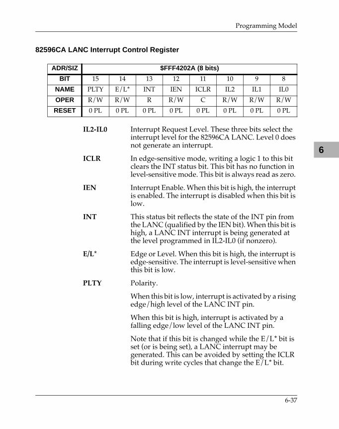
Programming Model
6
82596CA LANC Interrupt Control Register
IL2-IL0 Interrupt Request Level. These three bits select the interrupt level for the 82596CA LANC. Level 0 does not generate an interrupt.
ICLR In edge-sensitive mode, writing a logic 1 to this bit clears the INT status bit. This bit has no function in level-sensitive mode. This bit is always read as zero.
IEN Interrupt Enable. When this bit is high, the interrupt is enabled. The interrupt is disabled when this bit is low.
INT This status bit reflects the state of the INT pin from the LANC (qualified by the IEN bit). When this bit is high, a LANC INT interrupt is being generated at the level programmed in IL2-IL0 (if nonzero).
E/L* Edge or Level. When this bit is high, the interrupt is edge-sensitive. The interrupt is level-sensitive when this bit is low.
PLTY Polarity.
When this bit is low, interrupt is activated by a rising edge/high level of the LANC INT pin.
When this bit is high, interrupt is activated by a falling edge/low level of the LANC INT pin.
Note that if this bit is changed while the E/L* bit is set (or is being set), a LANC interrupt may be generated. This can be avoided by setting the ICLR bit during write cycles that change the E/L* bit.
ADR/SIZ $FFF4202A (8 bits)
BIT 15 14 13 12 11 10 9 8
NAME PLTY E/L* INT IEN ICLR IL2 IL1 IL0
OPER R/W R/W R R/W C R/W R/W R/W
RESET 0 PL 0 PL 0 PL 0 PL 0 PL 0 PL 0 PL 0 PL
6-37
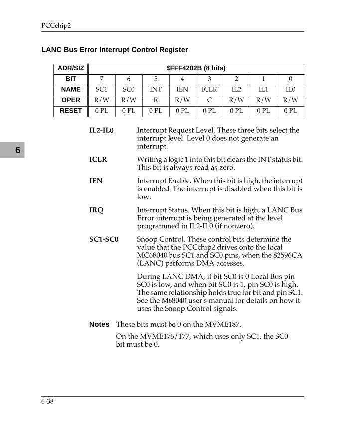
PCCchip2
6
LANC Bus Error Interrupt Control Register
IL2-IL0 Interrupt Request Level. These three bits select the interrupt level. Level 0 does not generate an interrupt.
ICLR Writing a logic 1 into this bit clears the INT status bit. This bit is always read as zero.
IEN Interrupt Enable. When this bit is high, the interrupt is enabled. The interrupt is disabled when this bit is low.
IRQ Interrupt Status. When this bit is high, a LANC Bus Error interrupt is being generated at the level programmed in IL2-IL0 (if nonzero).
SC1-SC0 Snoop Control. These control bits determine the value that the PCCchip2 drives onto the local MC68040 bus SC1 and SC0 pins, when the 82596CA (LANC) performs DMA accesses.
During LANC DMA, if bit SC0 is 0 Local Bus pin SC0 is low, and when bit SC0 is 1, pin SC0 is high. The same relationship holds true for bit and pin SC1. See the M68040 user's manual for details on how it uses the Snoop Control signals.
Notes These bits must be 0 on the MVME187.
On the MVME176/177, which uses only SC1, the SC0 bit must be 0.
ADR/SIZ $FFF4202B (8 bits)
BIT 7 6 5 4 3 2 1 0
NAME SC1 SC0 INT IEN ICLR IL2 IL1 IL0
OPER R/W R/W R R/W C R/W R/W R/W
RESET 0 PL 0 PL 0 PL 0 PL 0 PL 0 PL 0 PL 0 PL
6-38
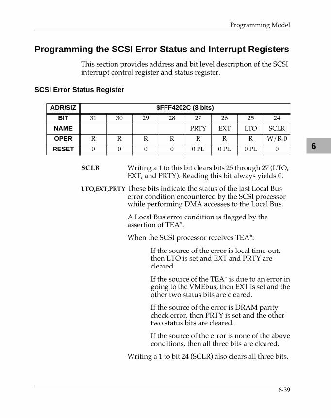
Programming Model
6
Programming the SCSI Error Status and Interrupt Registers
This section provides address and bit level description of the SCSI interrupt control register and status register.
SCSI Error Status Register
SCLR Writing a 1 to this bit clears bits 25 through 27 (LTO, EXT, and PRTY). Reading this bit always yields 0.
LTO,EXT,PRTY These bits indicate the status of the last Local Bus error condition encountered by the SCSI processor while performing DMA accesses to the Local Bus.
A Local Bus error condition is flagged by the assertion of TEA*.
When the SCSI processor receives TEA*:
If the source of the error is local time-out,then LTO is set and EXT and PRTY arecleared.
If the source of the TEA* is due to an error ingoing to the VMEbus, then EXT is set and theother two status bits are cleared.
If the source of the error is DRAM paritycheck error, then PRTY is set and the othertwo status bits are cleared.
If the source of the error is none of the aboveconditions, then all three bits are cleared.
Writing a 1 to bit 24 (SCLR) also clears all three bits.
ADR/SIZ $FFF4202C (8 bits)
BIT 31 30 29 28 27 26 25 24
NAME PRTY EXT LTO SCLR
OPER R R R R R R R W/R-0
RESET 0 0 0 0 0 PL 0 PL 0 PL 0
6-39
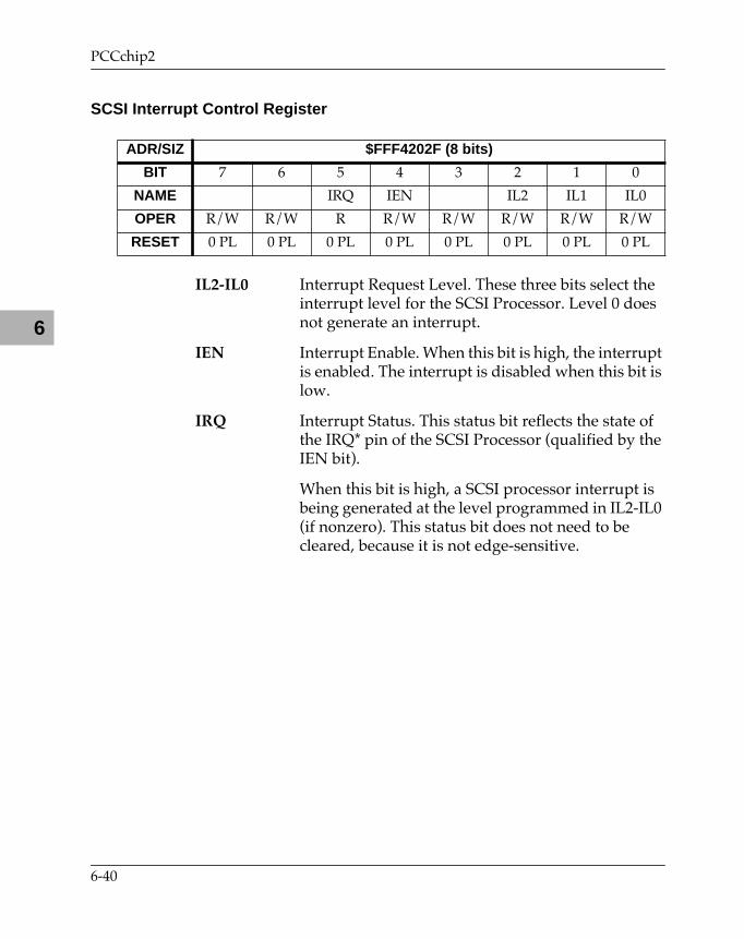
PCCchip2
6
SCSI Interrupt Control Register
IL2-IL0 Interrupt Request Level. These three bits select the interrupt level for the SCSI Processor. Level 0 does not generate an interrupt.
IEN Interrupt Enable. When this bit is high, the interrupt is enabled. The interrupt is disabled when this bit is low.
IRQ Interrupt Status. This status bit reflects the state of the IRQ* pin of the SCSI Processor (qualified by the IEN bit).
When this bit is high, a SCSI processor interrupt is being generated at the level programmed in IL2-IL0 (if nonzero). This status bit does not need to be cleared, because it is not edge-sensitive.
ADR/SIZ $FFF4202F (8 bits)
BIT 7 6 5 4 3 2 1 0
NAME IRQ IEN IL2 IL1 IL0
OPER R/W R/W R R/W R/W R/W R/W R/W
RESET 0 PL 0 PL 0 PL 0 PL 0 PL 0 PL 0 PL 0 PL
6-40
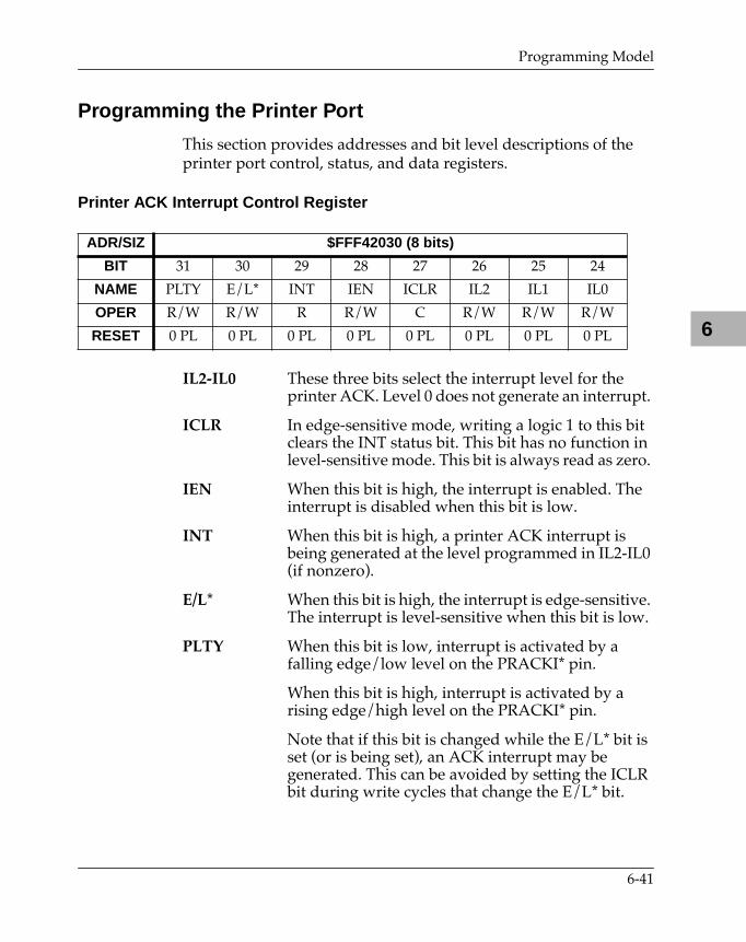
Programming Model
6
Programming the Printer Port
This section provides addresses and bit level descriptions of the printer port control, status, and data registers.
Printer ACK Interrupt Control Register
IL2-IL0 These three bits select the interrupt level for the printer ACK. Level 0 does not generate an interrupt.
ICLR In edge-sensitive mode, writing a logic 1 to this bit clears the INT status bit. This bit has no function in level-sensitive mode. This bit is always read as zero.
IEN When this bit is high, the interrupt is enabled. The interrupt is disabled when this bit is low.
INT When this bit is high, a printer ACK interrupt is being generated at the level programmed in IL2-IL0 (if nonzero).
E/L* When this bit is high, the interrupt is edge-sensitive. The interrupt is level-sensitive when this bit is low.
PLTY When this bit is low, interrupt is activated by a falling edge/low level on the PRACKI* pin.
When this bit is high, interrupt is activated by a rising edge/high level on the PRACKI* pin.
Note that if this bit is changed while the E/L* bit is set (or is being set), an ACK interrupt may be generated. This can be avoided by setting the ICLR bit during write cycles that change the E/L* bit.
ADR/SIZ $FFF42030 (8 bits)
BIT 31 30 29 28 27 26 25 24
NAME PLTY E/L* INT IEN ICLR IL2 IL1 IL0
OPER R/W R/W R R/W C R/W R/W R/W
RESET 0 PL 0 PL 0 PL 0 PL 0 PL 0 PL 0 PL 0 PL
6-41
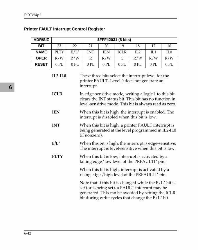
PCCchip2
6
Printer FAULT Interrupt Control Register
IL2-IL0 These three bits select the interrupt level for the printer FAULT. Level 0 does not generate an interrupt.
ICLR In edge-sensitive mode, writing a logic 1 to this bit clears the INT status bit. This bit has no function in level-sensitive mode. This bit is always read as zero.
IEN When this bit is high, the interrupt is enabled. The interrupt is disabled when this bit is low.
INT When this bit is high, a printer FAULT interrupt is being generated at the level programmed in IL2-IL0 (if nonzero).
E/L* When this bit is high, the interrupt is edge-sensitive. The interrupt is level-sensitive when this bit is low.
PLTY When this bit is low, interrupt is activated by a falling edge/low level of the PRFAULTI* pin.
When this bit is high, interrupt is activated by a rising edge /high level of the PRFAULTI* pin.
Note that if this bit is changed while the E/L* bit is set (or is being set), a FAULT interrupt may be generated. This can be avoided by setting the ICLR bit during write cycles that change the E/L* bit.
ADR/SIZ $FFF42031 (8 bits)
BIT 23 22 21 20 19 18 17 16
NAME PLTY E/L* INT IEN ICLR IL2 IL1 IL0
OPER R/W R/W R R/W C R/W R/W R/W
RESET 0 PL 0 PL 0 PL 0 PL 0 PL 0 PL 0 PL 0 PL
6-42
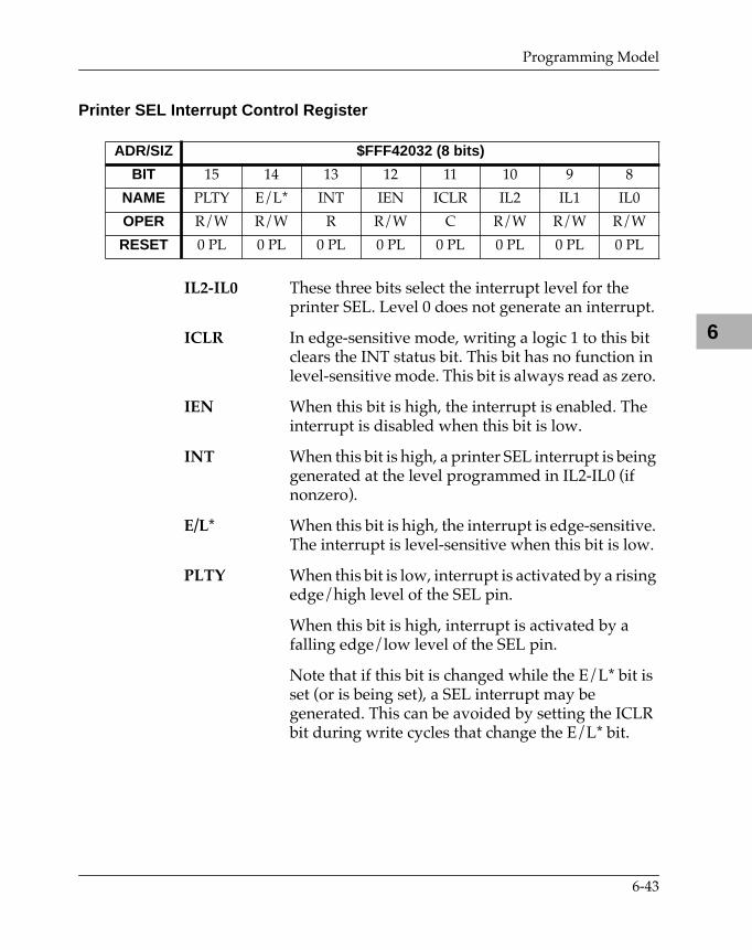
Programming Model
6
Printer SEL Interrupt Control Register
IL2-IL0 These three bits select the interrupt level for the printer SEL. Level 0 does not generate an interrupt.
ICLR In edge-sensitive mode, writing a logic 1 to this bit clears the INT status bit. This bit has no function in level-sensitive mode. This bit is always read as zero.
IEN When this bit is high, the interrupt is enabled. The interrupt is disabled when this bit is low.
INT When this bit is high, a printer SEL interrupt is being generated at the level programmed in IL2-IL0 (if nonzero).
E/L* When this bit is high, the interrupt is edge-sensitive. The interrupt is level-sensitive when this bit is low.
PLTY When this bit is low, interrupt is activated by a rising edge/high level of the SEL pin.
When this bit is high, interrupt is activated by a falling edge/low level of the SEL pin.
Note that if this bit is changed while the E/L* bit is set (or is being set), a SEL interrupt may be generated. This can be avoided by setting the ICLR bit during write cycles that change the E/L* bit.
ADR/SIZ $FFF42032 (8 bits)
BIT 15 14 13 12 11 10 9 8
NAME PLTY E/L* INT IEN ICLR IL2 IL1 IL0
OPER R/W R/W R R/W C R/W R/W R/W
RESET 0 PL 0 PL 0 PL 0 PL 0 PL 0 PL 0 PL 0 PL
6-43

PCCchip2
6
Printer PE Interrupt Control Register
IL2-IL0 These three bits select the interrupt level for the printer PE. Level 0 does not generate an interrupt.
ICLR In edge-sensitive mode, writing a logic 1 to this bit clears the INT status bit. This bit has no function in level-sensitive mode. This bit is always read as zero.
IEN When this bit is high, the interrupt is enabled. The interrupt is disabled when this bit is low.
INT When this bit is high, a printer PE interrupt is being generated at the level programmed in IL2-IL0 (if nonzero).
E/L* When this bit is high, the interrupt is edge-sensitive. The interrupt is level-sensitive when this bit is low.
PLTY When this bit is low, interrupt is activated by a rising edge/high level of the PE pin.
When this bit is high, interrupt is activated by a falling edge/low level of the PE pin.
Note that if this bit is changed while the E/L* bit is set (or is being set), a PE interrupt may be generated. This can be avoided by setting the ICLR bit during write cycles that change the E/L* bit.
ADR/SIZ $FFF42033 (8 bits)
BIT 7 6 5 4 3 2 1 0
NAME PLTY E/L* INT IEN ICLR IL2 IL1 IL0
OPER R/W R/W R R/W C R/W R/W R/W
RESET 0 PL 0 PL 0 PL 0 PL 0 PL 0 PL 0 PL 0 PL
6-44
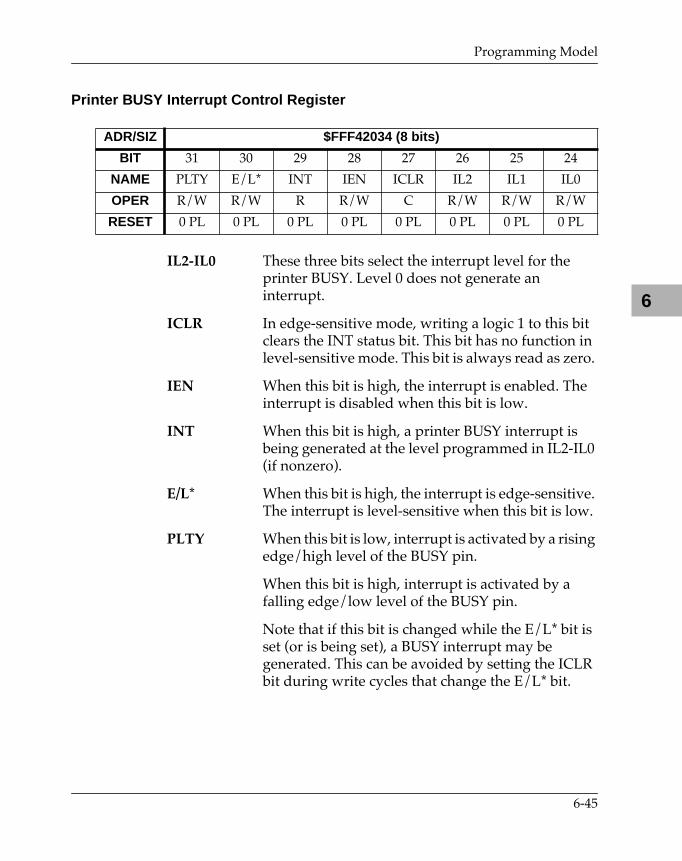
Programming Model
6
Printer BUSY Interrupt Control Register
IL2-IL0 These three bits select the interrupt level for the printer BUSY. Level 0 does not generate an interrupt.
ICLR In edge-sensitive mode, writing a logic 1 to this bit clears the INT status bit. This bit has no function in level-sensitive mode. This bit is always read as zero.
IEN When this bit is high, the interrupt is enabled. The interrupt is disabled when this bit is low.
INT When this bit is high, a printer BUSY interrupt is being generated at the level programmed in IL2-IL0 (if nonzero).
E/L* When this bit is high, the interrupt is edge-sensitive. The interrupt is level-sensitive when this bit is low.
PLTY When this bit is low, interrupt is activated by a rising edge/high level of the BUSY pin.
When this bit is high, interrupt is activated by a falling edge/low level of the BUSY pin.
Note that if this bit is changed while the E/L* bit is set (or is being set), a BUSY interrupt may be generated. This can be avoided by setting the ICLR bit during write cycles that change the E/L* bit.
ADR/SIZ $FFF42034 (8 bits)
BIT 31 30 29 28 27 26 25 24
NAME PLTY E/L* INT IEN ICLR IL2 IL1 IL0
OPER R/W R/W R R/W C R/W R/W R/W
RESET 0 PL 0 PL 0 PL 0 PL 0 PL 0 PL 0 PL 0 PL
6-45
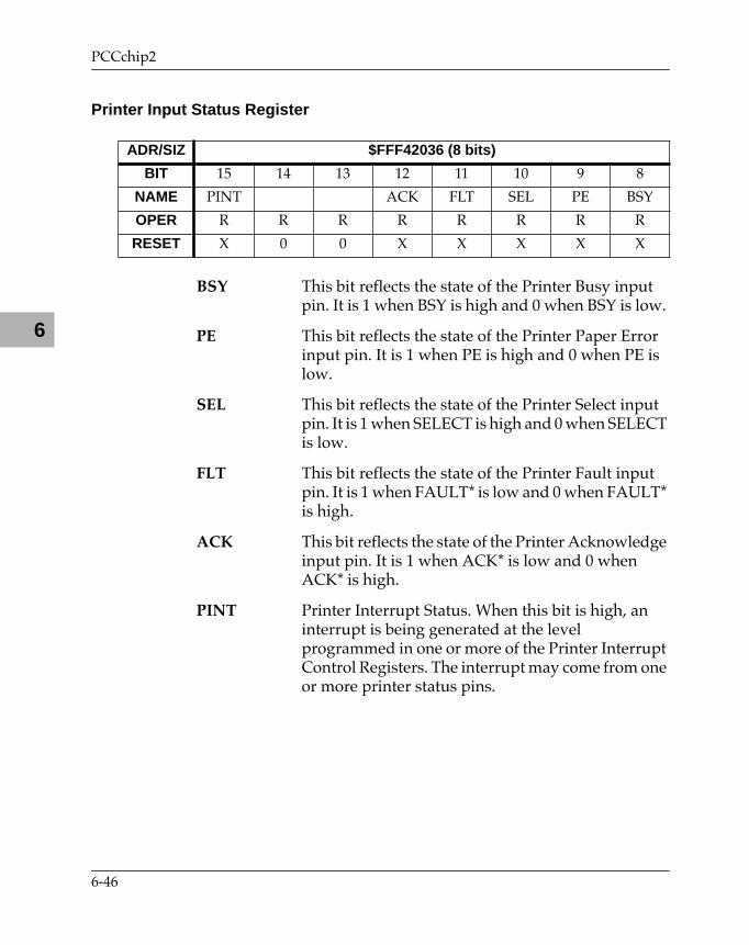
PCCchip2
6
Printer Input Status Register
BSY This bit reflects the state of the Printer Busy input pin. It is 1 when BSY is high and 0 when BSY is low.
PE This bit reflects the state of the Printer Paper Error input pin. It is 1 when PE is high and 0 when PE is low.
SEL This bit reflects the state of the Printer Select input pin. It is 1 when SELECT is high and 0 when SELECT is low.
FLT This bit reflects the state of the Printer Fault input pin. It is 1 when FAULT* is low and 0 when FAULT* is high.
ACK This bit reflects the state of the Printer Acknowledge input pin. It is 1 when ACK* is low and 0 when ACK* is high.
PINT Printer Interrupt Status. When this bit is high, an interrupt is being generated at the level programmed in one or more of the Printer Interrupt Control Registers. The interrupt may come from one or more printer status pins.
ADR/SIZ $FFF42036 (8 bits)
BIT 15 14 13 12 11 10 9 8
NAME PINT ACK FLT SEL PE BSY
OPER R R R R R R R R
RESET X 0 0 X X X X X
6-46
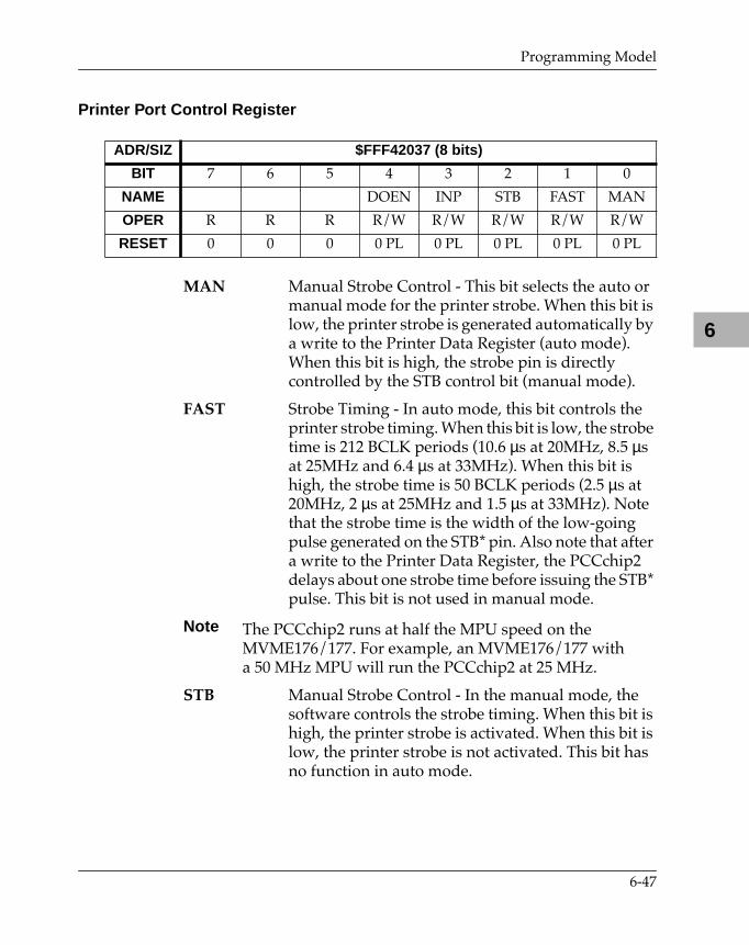
Programming Model
6
Printer Port Control Register
MAN Manual Strobe Control - This bit selects the auto or manual mode for the printer strobe. When this bit is low, the printer strobe is generated automatically by a write to the Printer Data Register (auto mode). When this bit is high, the strobe pin is directly controlled by the STB control bit (manual mode).
FAST Strobe Timing - In auto mode, this bit controls the printer strobe timing. When this bit is low, the strobe time is 212 BCLK periods (10.6 µs at 20MHz, 8.5 µs at 25MHz and 6.4 µs at 33MHz). When this bit is high, the strobe time is 50 BCLK periods (2.5 µs at 20MHz, 2 µs at 25MHz and 1.5 µs at 33MHz). Note that the strobe time is the width of the low-going pulse generated on the STB* pin. Also note that after a write to the Printer Data Register, the PCCchip2 delays about one strobe time before issuing the STB* pulse. This bit is not used in manual mode.
Note The PCCchip2 runs at half the MPU speed on the MVME176/177. For example, an MVME176/177 with a 50 MHz MPU will run the PCCchip2 at 25 MHz.
STB Manual Strobe Control - In the manual mode, the software controls the strobe timing. When this bit is high, the printer strobe is activated. When this bit is low, the printer strobe is not activated. This bit has no function in auto mode.
ADR/SIZ $FFF42037 (8 bits)
BIT 7 6 5 4 3 2 1 0
NAME DOEN INP STB FAST MAN
OPER R R R R/W R/W R/W R/W R/W
RESET 0 0 0 0 PL 0 PL 0 PL 0 PL 0 PL
6-47
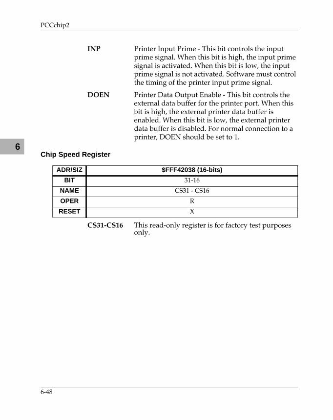
PCCchip2
6
INP Printer Input Prime - This bit controls the input prime signal. When this bit is high, the input prime signal is activated. When this bit is low, the input prime signal is not activated. Software must control the timing of the printer input prime signal.
DOEN Printer Data Output Enable - This bit controls the external data buffer for the printer port. When this bit is high, the external printer data buffer is enabled. When this bit is low, the external printer data buffer is disabled. For normal connection to a printer, DOEN should be set to 1.
Chip Speed Register
CS31-CS16 This read-only register is for factory test purposes only.
ADR/SIZ $FFF42038 (16-bits)
BIT 31-16
NAME CS31 - CS16
OPER R
RESET X
6-48
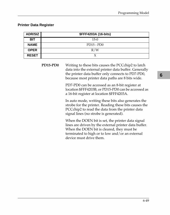
Programming Model
6
Printer Data Register
PD15-PD0 Writing to these bits causes the PCCchip2 to latch data into the external printer data buffer. Generally the printer data buffer only connects to PD7-PD0, because most printer data paths are 8 bits wide.
PD7-PD0 can be accessed as an 8-bit register at location $FFF4203B, or PD15-PD0 can be accessed as a 16-bit register at location $FFF4203A.
In auto mode, writing these bits also generates the strobe for the printer. Reading these bits causes the PCCchip2 to read the data from the printer data signal lines (no strobe is generated).
When the DOEN bit is set, the printer data signal lines are driven by the external printer data buffer. When the DOEN bit is cleared, they must be terminated to high or to low and/or an external device must drive them.
ADR/SIZ $FFF4203A (16-bits)
BIT 15-0
NAME PD15 - PD0
OPER R/W
RESET X
6-49
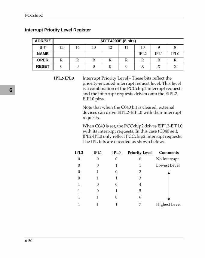
PCCchip2
6
Interrupt Priority Level Register
IPL2-IPL0 Interrupt Priority Level - These bits reflect the priority-encoded interrupt request level. This level is a combination of the PCCchip2 interrupt requests and the interrupt requests driven onto the EIPL2-EIPL0 pins.
Note that when the C040 bit is cleared, external devices can drive EIPL2-EIPL0 with their interrupt requests.
When C040 is set, the PCCchip2 drives EIPL2-EIPL0 with its interrupt requests. In this case (C040 set), IPL2-IPL0 only reflect PCCchip2 interrupt requests. The IPL bits are encoded as shown below:
ADR/SIZ $FFF4203E (8 bits)
BIT 15 14 13 12 11 10 9 8
NAME IPL2 IPL1 IPL0
OPER R R R R R R R R
RESET 0 0 0 0 0 X X X
IPL2 IPL1 IPL0 Priority Level Comments
0 0 0 0 No Interrupt
0 0 1 1 Lowest Level
0 1 0 2
0 1 1 3
1 0 0 4
1 0 1 5
1 1 0 6
1 1 1 7 Highest Level
6-50
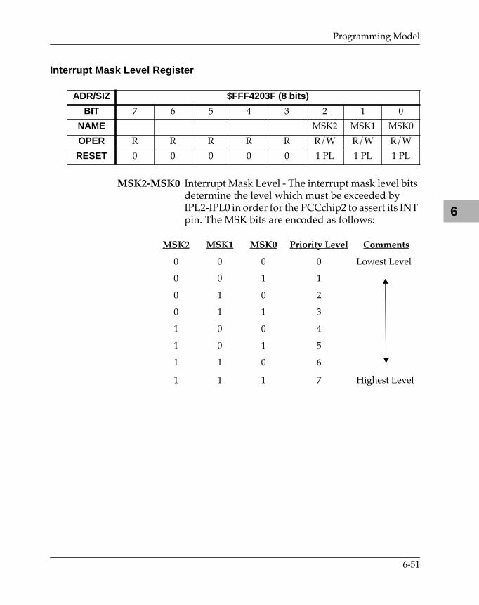
Programming Model
6
Interrupt Mask Level Register
MSK2-MSK0 Interrupt Mask Level - The interrupt mask level bits determine the level which must be exceeded by IPL2-IPL0 in order for the PCCchip2 to assert its INT pin. The MSK bits are encoded as follows:
ADR/SIZ $FFF4203F (8 bits)
BIT 7 6 5 4 3 2 1 0
NAME MSK2 MSK1 MSK0
OPER R R R R R R/W R/W R/W
RESET 0 0 0 0 0 1 PL 1 PL 1 PL
MSK2 MSK1 MSK0 Priority Level Comments
0 0 0 0 Lowest Level
0 0 1 1
0 1 0 2
0 1 1 3
1 0 0 4
1 0 1 5
1 1 0 6
1 1 1 7 Highest Level
6-51

PCCchip2
6
6-52
7
7MEMC040IntroductionThis chapter defines the four-way interleaving memory controller ASIC for the MC68040-type bus. This memory controller ASIC is referred to as the MEMC040 hereafter. The MEMC040 is designed for the MVME166/MVME167/MVME187 Single Board Computers and is to be used in conjunction with the data multiplexer ASIC (MEMMUX) and the address latch/multiplexer ASIC (AMUX) to provide the interface to a 144-bit wide DRAM memory system.
Note The MEMC040 is not used with the MVME176/177.
Summary of FeaturesThis section lists the features of the MEMC040 chip.
❏ Allows 2-1-1-1 memory accesses (sustained) for burst writes.
❏ Allows 4-1-1-1 memory accesses (sustained) for burst reads (5-1-1-1 with parity ON).
❏ One MEMC040 controls up to two contiguous blocks of 144-bit wide memory array.
❏ One MEMC040 controls up to 128MB of memory.
❏ Supports 1M, 4M, and 16M DRAM in either x1 or x4 configurations.
❏ Supports byte, two-byte, four-byte, and cache line read or write transfers.
❏ Supports write-per-bit x4 DRAM for parity memory.
7-1

MEMC040
7
❏ Provides an 8-bit status register and an 8-bit control register when write-per-bit DRAMs are not used.
❏ Programmable base address for the memory blocks.
❏ Programmable parity modes: ON, OFF, interrupt.
❏ Built-in refresh timer and refresh controller.
❏ Write-wrong parity control bit for test purposes.
Functional DescriptionThis section describes the MEMC040 in general and then in detail.
General Description
The MEMC040 is designed to be used with one AMUX address multiplexer ASIC, two MEMMUX data multiplexer ASICs, and x1 or x4 DRAM memory chips to form a memory system for an MC68040-type bus. This ASIC is used by the MVME166/167/187 Single Board Computers. The typical block diagram for such a memory scheme is shown in Figure 7-1.
Performance
The MEMC040 is specifically designed to provide maximum performance for cache line (burst) cycles to and from the MC68040-compatible local bus (Local Bus). This is done by providing a four-way interleave between the 32-bit MC68040 data bus and four separate banks of 32-bit DRAM. This permits burst accesses to be pipelined, giving high performance from standard speed DRAMs. For example, burst reads can be sustained at speeds of 7 clocks per line of four four-bytes (8 clocks per line with parity enabled). This gives an average access time of 1.75 clocks (2.0 clocks) per four-byte, or 70 nsec (80 nsec) at 25 MHz, while using 80 nsec DRAM. Burst writes can be sustained at 5 clocks per line, for an average of 1.25 clocks per four-byte, or 50 nsec at 25 MHz.
7-2
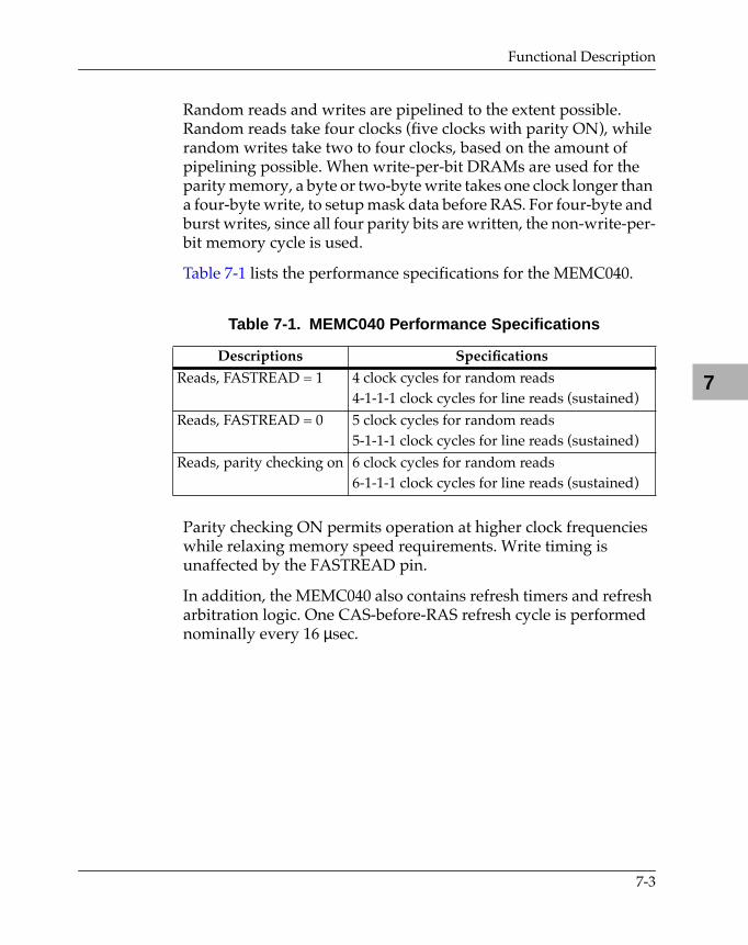
Functional Description
7
Random reads and writes are pipelined to the extent possible. Random reads take four clocks (five clocks with parity ON), while random writes take two to four clocks, based on the amount of pipelining possible. When write-per-bit DRAMs are used for the parity memory, a byte or two-byte write takes one clock longer than a four-byte write, to setup mask data before RAS. For four-byte and burst writes, since all four parity bits are written, the non-write-per-bit memory cycle is used.
Table 7-1 lists the performance specifications for the MEMC040.
Parity checking ON permits operation at higher clock frequencies while relaxing memory speed requirements. Write timing is unaffected by the FASTREAD pin.
In addition, the MEMC040 also contains refresh timers and refresh arbitration logic. One CAS-before-RAS refresh cycle is performed nominally every 16 µsec.
Table 7-1. MEMC040 Performance Specifications
Descriptions SpeciÞcations
Reads, FASTREAD = 1 4 clock cycles for random reads4-1-1-1 clock cycles for line reads (sustained)
Reads, FASTREAD = 0 5 clock cycles for random reads5-1-1-1 clock cycles for line reads (sustained)
Reads, parity checking on 6 clock cycles for random reads6-1-1-1 clock cycles for line reads (sustained)
7-3
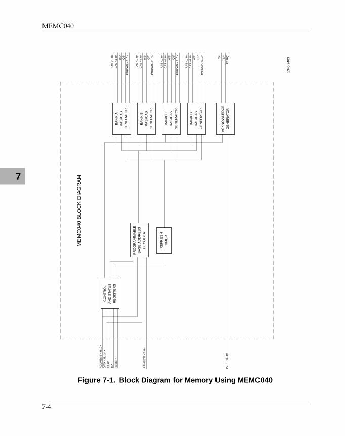
MEMC040
7
Figure 7-1. Block Diagram for Memory Using MEMC040
1345
940
3
AD
DR
ES
S <
31..0
>
DAT
A <
31..2
4>
RE
AD
RA
MS
IZE
<2.
.0>
PE
RR
<1.
.0>
TS
*R
ES
ET
*R
AS
<1.
.0>
CA
S <
4..0
>
WE
*Q
E*
PAR
DAT
A <
3..0
>
RA
S <
1..0
>C
AS
<4.
.0>
WE
*Q
E*
PAR
DAT
A <
3..0
>
RA
S <
1..0
>C
AS
<4.
.0>
WE
*Q
E*
PAR
DAT
A <
3..0
>
RA
S <
1..0
>C
AS
<4.
.0>
WE
*Q
E*
PAR
DAT
A <
3..0
>
TA*
TE
A*
PE
IRQ
*
BA
NK
A
RA
S/C
AS
GE
NE
RAT
OR
BA
NK
B
RA
S/C
AS
GE
NE
RAT
OR
BA
NK
C
RA
S/C
AS
GE
NE
RAT
OR
BA
NK
D
RA
S/C
AS
GE
NE
RAT
OR
AC
KN
OW
LED
GE
GE
NE
RAT
OR
RE
FR
ES
H
TIM
ER
PR
OG
RA
MM
AB
LE
BA
SE
AD
DR
ES
S
DE
CO
DE
R
ME
MC
040
BLO
CK
DIA
GR
AM
CO
NT
RO
L
AN
D S
TAT
US
RE
GIS
TE
RS
7-4
Functional Description
7
Status and Control Registers
The MEMC040 contains eight 8-bit registers that appear only at D31-D24. Burst reads and writes are not allowed to be executed to these registers, but byte, two-byte, or four-byte accesses may be used interchangeably. The base address of the first MEMC040 in a system is $FFF43000, and the base address of the second MEMC040 (if used) is $FFF43100.
Each register definition includes a table with 5 lines:
❏ Line 1 is the two base addresses of the register and the number of bits defined in the table.
❏ Line 2 shows the bits defined by this table.
❏ Line 3 defines the name of the register or the name of the bits in the register.
❏ Line 4 defines the operations possible on the register bits as follows:
❏ Line 5 defines the state of the bit following a reset as follows.
Table 7-2 shows all MEMC040 internal registers.
R This bit is a read-only status bit. R/W This bit is readable and writable.
P The bit is affected by power-up reset. S The bit is affected by SYSRESET. L The bit is affected by local reset.X The bit is not affected by reset.0 This bit is always 0.1 This bit is always 1.
7-5
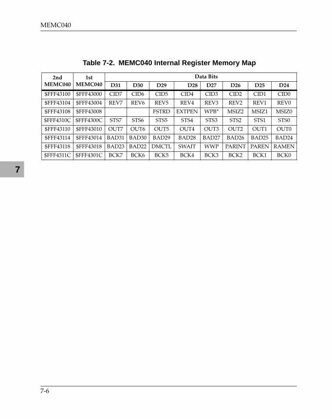
MEMC040
7
Table 7-2. MEMC040 Internal Register Memory Map
2nd MEMC040
1st MEMC040
Data Bits
D31 D30 D29 D28 D27 D26 D25 D24
$FFF43100 $FFF43000 CID7 CID6 CID5 CID4 CID3 CID2 CID1 CID0
$FFF43104 $FFF43004 REV7 REV6 REV5 REV4 REV3 REV2 REV1 REV0
$FFF43108 $FFF43008 FSTRD EXTPEN WPB* MSIZ2 MSIZ1 MSIZ0
$FFF4310C $FFF4300C STS7 STS6 STS5 STS4 STS3 STS2 STS1 STS0
$FFF43110 $FFF43010 OUT7 OUT6 OUT5 OUT4 OUT3 OUT2 OUT1 OUT0
$FFF43114 $FFF43014 BAD31 BAD30 BAD29 BAD28 BAD27 BAD26 BAD25 BAD24
$FFF43118 $FFF43018 BAD23 BAD22 DMCTL SWAIT WWP PARINT PAREN RAMEN
$FFF4311C $FFF4301C BCK7 BCK6 BCK5 BCK4 BCK3 BCK2 BCK1 BCK0
7-6
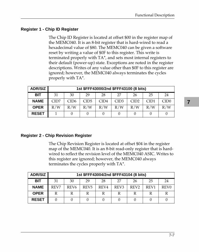
Functional Description
7
Register 1 - Chip ID Register
The Chip ID Register is located at offset $00 in the register map of the MEMC040. It is an 8-bit register that is hard-wired to read a hexadecimal value of $80. The MEMC040 can be given a software reset by writing a value of $0F to this register. This write is terminated properly with TA*, and sets most internal registers to their default (power-up) state. Exceptions are noted in the register descriptions. Writes of any value other than $0F to this register are ignored; however, the MEMC040 always terminates the cycles properly with TA*.
Register 2 - Chip Revision Register
The Chip Revision Register is located at offset $04 in the register map of the MEMC040. It is an 8-bit read-only register that is hard-wired to reflect the revision level of the MEMC040 ASIC. Writes to this register are ignored; however, the MEMC040 always terminates the cycles properly with TA*.
ADR/SIZ 1st $FFF43000/2nd $FFF43100 (8 bits)
BIT 31 30 29 28 27 26 25 24
NAME CID7 CID6 CID5 CID4 CID3 CID2 CID1 CID0
OPER R/W R/W R/W R/W R/W R/W R/W R/W
RESET 1 0 0 0 0 0 0 0
ADR/SIZ 1st $FFF43004/2nd $FFF43104 (8 bits)
BIT 31 30 29 28 27 26 25 24
NAME REV7 REV6 REV5 REV4 REV3 REV2 REV1 REV0
OPER R R R R R R R R
RESET 0 0 0 0 0 0 0 0
7-7
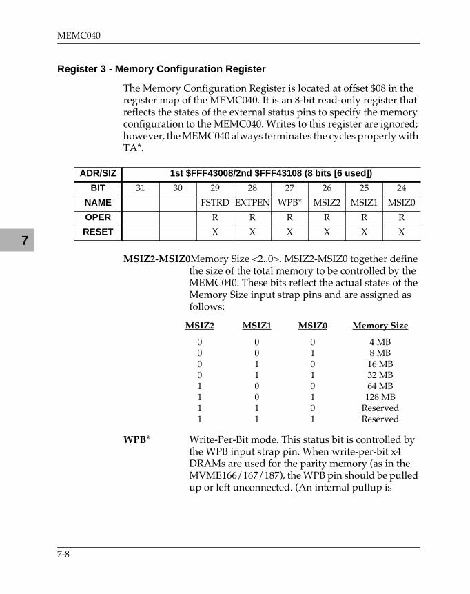
MEMC040
7
Register 3 - Memory Configuration Register
The Memory Configuration Register is located at offset $08 in the register map of the MEMC040. It is an 8-bit read-only register that reflects the states of the external status pins to specify the memory configuration to the MEMC040. Writes to this register are ignored; however, the MEMC040 always terminates the cycles properly with TA*.
MSIZ2-MSIZ0Memory Size <2..0>. MSIZ2-MSIZ0 together define the size of the total memory to be controlled by the MEMC040. These bits reflect the actual states of the Memory Size input strap pins and are assigned as follows:
WPB* Write-Per-Bit mode. This status bit is controlled by the WPB input strap pin. When write-per-bit x4 DRAMs are used for the parity memory (as in the MVME166/167/187), the WPB pin should be pulled up or left unconnected. (An internal pullup is
ADR/SIZ 1st $FFF43008/2nd $FFF43108 (8 bits [6 used])
BIT 31 30 29 28 27 26 25 24
NAME FSTRD EXTPEN WPB* MSIZ2 MSIZ1 MSIZ0
OPER R R R R R R
RESET X X X X X X
MSIZ2 MSIZ1 MSIZ0 Memory Size
00001111
00110011
01010101
4 MB8 MB16 MB32 MB64 MB128 MB
ReservedReserved
7-8
Functional Description
7
provided on this pin.) This bit is then read as a logic 0, and byte/two-byte writes utilize write-per-bit memory cycles.
If the MEMC040 is used in an application which does not use write-per-bit DRAMs for the parity memory, then the WPB input strap pin should be connected to a logic low or ground. This bit is then read as a logic one, and pins APD3-APD0 and BPD3-BPD0 become input pins and together form Status Register 4. Also, pins CPD3-CPD0 and DPD3-DPD0 are combined to form an 8-bit control register driven by Control Register 5.
EXTPEN External Parity Enable. This status bit reflects the state of the EXTPEN input pin. When EXTPEN is a logic 1, it enables the PAREN and PARINT control bits to determine the parity checking mode for the memory. If EXTPEN is at a logic 0, all parity checking and parity interrupts are disabled. An internal pullup is provided on this input pin, to assure a logic 1 if unconnected.
FSTRD Fast Read. This status bit reflects the state of the FASTREAD input pin. When this input is at a logic 1, the MEMC040 operates in the fast mode. When this input is at a logic 0, the MEMC040 operates in the slow mode. Timing for the fast and slow modes is given in the General Description section. Write timing is unaffected by this pin. An internal pullup is provided on this input pin, to assure a logic 1 if unconnected.
7-9
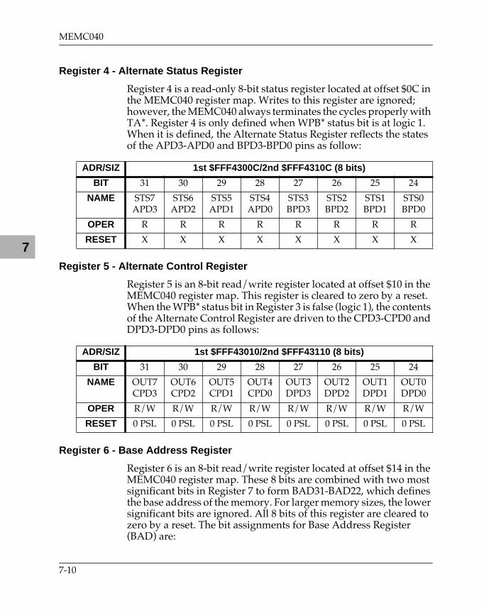
MEMC040
7
Register 4 - Alternate Status Register
Register 4 is a read-only 8-bit status register located at offset $0C in the MEMC040 register map. Writes to this register are ignored; however, the MEMC040 always terminates the cycles properly with TA*. Register 4 is only defined when WPB* status bit is at logic 1. When it is defined, the Alternate Status Register reflects the states of the APD3-APD0 and BPD3-BPD0 pins as follow:
Register 5 - Alternate Control Register
Register 5 is an 8-bit read/write register located at offset $10 in the MEMC040 register map. This register is cleared to zero by a reset. When the WPB* status bit in Register 3 is false (logic 1), the contents of the Alternate Control Register are driven to the CPD3-CPD0 and DPD3-DPD0 pins as follows:
Register 6 - Base Address Register
Register 6 is an 8-bit read/write register located at offset $14 in the MEMC040 register map. These 8 bits are combined with two most significant bits in Register 7 to form BAD31-BAD22, which defines the base address of the memory. For larger memory sizes, the lower significant bits are ignored. All 8 bits of this register are cleared to zero by a reset. The bit assignments for Base Address Register (BAD) are:
ADR/SIZ 1st $FFF4300C/2nd $FFF4310C (8 bits)
BIT 31 30 29 28 27 26 25 24
NAME STS7APD3
STS6APD2
STS5APD1
STS4APD0
STS3BPD3
STS2BPD2
STS1BPD1
STS0BPD0
OPER R R R R R R R R
RESET X X X X X X X X
ADR/SIZ 1st $FFF43010/2nd $FFF43110 (8 bits)
BIT 31 30 29 28 27 26 25 24
NAME OUT7CPD3
OUT6CPD2
OUT5CPD1
OUT4CPD0
OUT3DPD3
OUT2DPD2
OUT1DPD1
OUT0DPD0
OPER R/W R/W R/W R/W R/W R/W R/W R/W
RESET 0 PSL 0 PSL 0 PSL 0 PSL 0 PSL 0 PSL 0 PSL 0 PSL
7-10
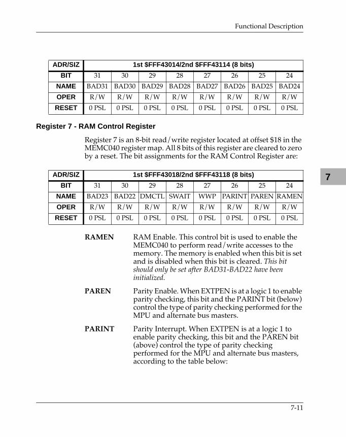
Functional Description
7
Register 7 - RAM Control Register
Register 7 is an 8-bit read/write register located at offset $18 in the MEMC040 register map. All 8 bits of this register are cleared to zero by a reset. The bit assignments for the RAM Control Register are:
RAMEN RAM Enable. This control bit is used to enable the MEMC040 to perform read/write accesses to the memory. The memory is enabled when this bit is set and is disabled when this bit is cleared. This bit should only be set after BAD31-BAD22 have been initialized.
PAREN Parity Enable. When EXTPEN is at a logic 1 to enable parity checking, this bit and the PARINT bit (below) control the type of parity checking performed for the MPU and alternate bus masters.
PARINT Parity Interrupt. When EXTPEN is at a logic 1 to enable parity checking, this bit and the PAREN bit (above) control the type of parity checking performed for the MPU and alternate bus masters, according to the table below:
ADR/SIZ 1st $FFF43014/2nd $FFF43114 (8 bits)
BIT 31 30 29 28 27 26 25 24
NAME BAD31 BAD30 BAD29 BAD28 BAD27 BAD26 BAD25 BAD24
OPER R/W R/W R/W R/W R/W R/W R/W R/W
RESET 0 PSL 0 PSL 0 PSL 0 PSL 0 PSL 0 PSL 0 PSL 0 PSL
ADR/SIZ 1st $FFF43018/2nd $FFF43118 (8 bits)
BIT 31 30 29 28 27 26 25 24
NAME BAD23 BAD22 DMCTL SWAIT WWP PARINT PAREN RAMEN
OPER R/W R/W R/W R/W R/W R/W R/W R/W
RESET 0 PSL 0 PSL 0 PSL 0 PSL 0 PSL 0 PSL 0 PSL 0 PSL
7-11
MEMC040
7
NoneÓ means no parity checking. Parity errors are not detected or reported. ÒInterruptÓ means that the MPU receives a parity interrupt if a parity error occurs. The bus cycle is terminated with TEA, and runs at the same speed as unchecked cycles. ÒCheckedÓ means that the cycle is terminated by TEA if a parity error occurs, and requires one more clock than unchecked cycles. When EXTPEN is low, parity checking is disabled for all bus masters, regardless of the state of PAREN or PARINT. When the interrupt mode is selected, the Parity Error Interrupt in the VMEchip2 must be enabled.
WWP Write Wrong Parity. The state of this control bit is driven to the WWP pin. A logic 1 means that external logic (i.e., the MEMMUX) should present wrong parity to the DRAM, to test the parity generation/checking circuits.
SWAIT Snoop Wait. When SWAIT is at logic 0, the MEMC040 does not wait for MI* (Memory Inhibit signal from MC68040) to be negated before starting a read access or a line push (burst write). When SWAIT is at logic 1, the MEMC040 waits for MI* (Memory Inhibit signal from MC68040) to be negated before starting any memory accesses.
DMCTL Data Mux Control. This bit is cleared to logic 0 at reset and must remain clear for all memory cycles in the MVME166/167/187 application. If this bit is set, the MEMMUX performs read-modify-write operations to the parity DRAMs for byte or two-byte writes. The MVME166/167/187 uses write-per-bit DRAMs, with the MEMC040 providing the write-per-bit support. This bit may be toggled for testing purposes while the RAMEN bit is cleared.
PAREN PARINT MPU Alternate
0011
0101
NoneInterruptCheckedInterrupt
NoneNone
CheckedChecked
7-12
Functional Description
7
BAD23-BAD22 These two bits are combined with all eight bits in Register 7 to form BAD31-BAD22 to define the base address of the memory. For larger memory sizes, the lower significant bits are ignored.
Register 8 - Bus Clock Register
Bus Clock Register is an 8-bit read/write register located at offset $1C in the MEMC040 register map. It should be programmed with the hexadecimal value of the operating clock frequency in MHz (i.e. $21 for 33 MHz). The MEMC040 uses the value programmed in this register to control the refresh timer so that the DRAMs are refreshed every 15.6 microseconds. After power-up, this register is initialized to $10 (for 16 MHz).
Note This register is configured only at the rising edge of the POR* (Power-Up Reset) pin of the MEMC040, and is unchanged by the software reset from the Chip ID Register or the RESET* pin.
The refresh rate is defined by the following equation:
refresh rate = BCK / bus clock * 16
where BCK is the value programmed in the Bus Clock Register, and bus clock is the board bus clock frequency.
For example, on a 25-MHz board, the refresh rate is:
25 / 25M * 16 = 16 µs
ADR/SIZ 1st $FFF4301C/2nd $FFF4311C (8 bits)
BIT 31 30 29 28 27 26 25 24
NAME BCK7 BCK6 BCK5 BCK4 BCK3 BCK2 BCK1 BCK0
OPER R/W R/W R/W R/W R/W R/W R/W R/W
RESET 0 P 0 P 0 P 0 P 0 P 0 P 0 P 0 P
7-13
MEMC040
7
7-14
8
8MCECCIntroductionThis chapter describes the ECC DRAM Controller ASIC (MCECC) used on the memory mezzanine boards with ECC protection. The MCECC is designed for the Single Board Computers described in this manual and is used in a set of two, to provide the interface to a 144-bit wide DRAM memory system.
Summary of FeaturesThis section lists the features of the MCECC chip.
❏ Allows 2-1-1-1 memory accesses (sustained) for burst writes.
❏ Allows 4-1-1-1 memory accesses (sustained) for burst reads (5-1-1-1 with BERR on or when FSTRD is cleared).
❏ Supports byte, two-byte, four-byte, and cache line read or write transfers.
❏ Programmable base address for DRAM.
❏ Built-in refresh timer and refresh controller.
❏ ECC:
Ð Single Bit Error Detect and Correct.
Ð Software enabled interrupt on Single Bit Error.
Ð Address and Syndrome Register for Single Bit Error logging support.
Ð Double Bit Error detect.
Ð Software programmable bus error and/or interrupt on Double Bit Error.
❏ Programmable period automatic scrub operation.
8-1
MCECC
8
Functional DescriptionThe following sections provide an overview of the functions provided by the MCECC. A detailed programming model for the MCECC control and status registers is provided in the section on Programming Model.
General Description
The MCECC is designed to be used as a set of two chips. A pair of MCECCs works with x4 DRAM memory chips to form a memory system. A pair of MCECCs that is connected to implement a memory control function is referred to as an ÒMCECC pairÓ. The MCECC pair provides all the functions required to implement a memory system. These include programmable map decoding, memory control, refresh, and a scrubber. The scrubber, when it is enabled, periodically scans memory looking for errors. If the scrubber finds a single bit error in the memory array, it corrects the error. This prevents soft single bit errors from becoming double bit errors.
Performance
The MCECC pair is specifically designed to provide maximum performance for cache line (burst) cycles to and from the MC68040 bus. This is done by providing a four-way interleave between the 32-bit MC68040-type data bus and the 128 bit (144 with check bits) DRAM. This permits burst accesses to be pipelined, giving high performance from standard speed, static column DRAMs. For example, burst reads can be sustained at speeds of 7 clocks per line of four four-bytes (8 clocks per line with BERR enabled or FSTRD cleared). If the local MC68040 bus clock frequency is 25MHz, this gives an average access time of 70ns (80ns with BERR or no FSTRD) per four-byte. Burst writes can be sustained at 5 clocks per line, for an average of 50ns at 33 MHz.
Random (non-burst) reads and writes are pipelined to the extent possible. Random reads take four clocks (five clocks with BERR on or FSTRD cleared).
8-2
Functional Description
8
Random, non-burst writes are the slowest kind of access because they require that the MCECC pair perform a read-modify-write cycle to the DRAM in order to complete. The MCECC pair responds to the local bus in two clocks during random writes, but then it takes another eight clocks for the DRAM read-modify-write cycle to complete, thereby making the effective cycle time 10 clocks if the following access by the local bus master is to DRAM. This amounts to two clocks for one random write, and 10 clocks for sustained random writes.
The performance specifications for the MCECC are shown in Table 8-1.
Cache Coherency
The MCECC pair supports the MC68040 caching scheme on the local bus by always providing 32 bits of valid data during DRAM read cycles regardless of the number of bytes requested by the local bus master for the cycle. It also supports cache coherency by monitoring the snoop control signal lines on the local bus and behaving appropriately based on their value.
When the snoop control signal lines (SC1, SC0) indicate that snooping is inhibited, the MCECC pair ignores the memory inhibit (MI*) signal line.
Table 8-1. MCECC Performance Specifications
Descriptions SpeciÞcations
Reads, BERR off, FSTRD = 1 4 clock cycles for random reads4-1-1-1 clock cycles for burst reads (sustained)
Reads, FSTRD = 0 5 clock cycles for random reads5-1-1-1 clock cycles for burst reads (sustained)
Reads, BERR on 5 clock cycles for random reads5-1-1-1 clock cycles for burst reads (sustained)
Writes 2 to 10 clock cycles for random non-burst writes2-1-1-1 clock cycles for burst writes (sustained)
8-3
MCECC
8
When (SC1, SC0) do not indicate that snooping is inhibited, the MCECC pair responds differently to DRAM accesses, based on whether the cycle is a read or a write, and on the snoop wait (SWAIT) control bit.
For a read with SWAIT = 0, the MCECC pair immediately starts a read cycle to the DRAM and latches the data from the DRAMs. It waits, however, for MI* to be negated before it enables the data (that has been latched) onto the local bus and asserts TA* or TEA*. If TA* or TEA* is asserted by another local bus slave before MI* is negated, then the MCECC pair assumes that the cycle is over and that the DRAM is not to participate in that cycle.
For a read with SWAIT = 1, the MCECC pair behaves the same as with SWAIT = 0 except that it does not start the DRAM read cycle until it sees the MI* signal negated. Note that this means that if another local bus slave asserts TA* or TEA* before MI* is negated, then the MCECC pair never starts the DRAM read cycle.
For a write cycle, the MCECC pair always waits for MI* to be negated before it begins a write cycle to the DRAM. If another local bus slave asserts TA* or TEA* before MI* is negated, then the MCECC pair never starts the DRAM write cycle.
ECC
The MCECC pair performs single bit error correction and double bit error detection (SECDED). The 32 bit wide local data bus is divided into lower (D00-D15) and upper (D16-D31) halves. Each half is routed through an MCECC, which multiplexes it with half of the 128 bit wide DRAM. This allows each MCECC to connect to 64 bits of the DRAM. Each MCECC additionally connects to 8 bits of check bit DRAM. This actually makes the DRAM array 144 bits wide (128 bits of normal data and 16 bits of check data).
Cycle Types
To support ECC, the MCECC pair always deals with DRAM using full width (144 bits, 72 bits for each MCECC) accesses. When the local bus master requests any size read of DRAM, the MCECC pair
8-4
Functional Description
8
reads 144 bits. When the local bus master requests a line write to DRAM, the MCECC pair writes all 144 bits. When the local bus master requests a byte, word (two-byte), or longword write to DRAM, the MCECC pair performs a 144-bit wide read cycle to DRAM, merges the appropriate local bus write data in, and writes 144 bits to DRAM.
Error Reporting
The MCECCs generate the ECC check bits for write cycles. They also check read data from the DRAM and correct it if it contains a single bit error. If a non-correctable error occurs within either of the MCECC 72 bits of read data, the affected MCECC indicates it by asserting its non-correctable error (NCE*) pin.
The following paragraphs indicate the actions taken by the MCECC pair for different error situations.
Single Bit Error (Cycle Type = Burst Read or Non-Burst Read)
Correct the Data that is driven to the local MC68040 bus.
Do not correct the Data in DRAM. Note that the DRAM is not corrected until the next scrub of that address, which happens only if scrubbing is enabled.
Terminate the cycle normally. (Assert TA to the local bus.)
Log the error if one has not already been logged.
Notify the local MPU via interrupt if so enabled.
Double Bit Error (Cycle Type = Burst Read or Non-Burst Read)
Cannot correct the data that is driven to the local MC68040 bus.
Leave the error in DRAM. (Note that it is not corrected in DRAM during the next scrub of that address.)
Terminate the cycle with Bus Error (assert TEA to the local bus) if so enabled.
8-5
MCECC
8
Log the error if one has not already been logged.
Notify the local MPU via interrupt if so enabled.
Triple (or Greater) Bit Error (Cycle Type = Burst Read or Non-Burst Read)
Some of these errors are detected correctly and are treated the same as a double bit error. The rest could show up as Òno errorÓ or Òsingle bit errorÓ, both of which are incorrect.
Cycle Type = Burst Write
Because all of the bits are written during a burst write, no checking is done.
Single Bit Error (Cycle Type = Non-Burst Write)
Correct the data read from the DRAM, merge with the write data, and write the correct, merged data to the DRAM.
Terminate the cycle normally. (Assert TA to the local bus.)
Log the error if one has not already been logged.
Notify the local MPU via interrupt if so enabled.
Double Bit Error (Cycle Type = Non-Burst Write)
Do not perform the write portion of the cycle. This causes the location to continue to indicate non-correctable error when accessed.
Terminate the cycle normally. (Assert TA to the local bus.)
Log the error if one has not already been logged.
Notify the local MPU via interrupt if so enabled.
Triple (or Greater) Bit Error (Cycle Type = Non-Burst Write)
Some of these errors are detected correctly and are treated the same as a double bit error. The rest could show up as Òno errorÓ or Òsingle bit errorÓ, both of which are incorrect.
8-6
Functional Description
8
Single Bit Error (Cycle Type = Scrub)
Write corrected data to the DRAM.
Log the error if one has not already been logged.
Notify the local MPU via interrupt if so enabled.
Double Bit Error (Cycle Type = Scrub)
Do not perform the write portion of the cycle. This causes the location to continue to indicate non-correctable error when accessed.
Log the error if one has not already been logged.
Notify the local MPU via interrupt if so enabled.
Triple (or Greater) Bit Error (Cycle Type = Scrub)
Some of these errors are detected correctly and are treated the same as a double bit error. The rest could show up as Òno errorÓ or Òsingle bit errorÓ, both of which are incorrect.
Error Logging
ECC error logging is facilitated by the MCECC because of its internal latches. When an error (single or double bit) occurs in the DRAMs to which an MCECC is connected, it freezes the address of the error and the syndrome bits associated with the data that is in error. Each MCECC performs this logging function independently of the other. Once an MCECC has logged an error, it does not log any new errors that occur until the ERRLOG control/status bit has been cleared by software.
Scrub
The MCECC pair contains programmable registers and circuitry that provide the scrubbing function. Programmable registers determine how often the entire DRAM is scrubbed. During a scrub,
8-7
MCECC
8
the scrubber holds the memory for a programmable amount of time, then releases it for the local bus, or refresher if one of them is requesting local bus mastership. The scrubber then refrains from using the DRAM again for a programmable amount of time. Each scrub cycle is made up of a full 144-bit read of DRAM, a correction of any single bit errors, and a write of the full 144 corrected bits back to the same location. If a single or double bit error occurs, the local bus master is notified if such interrupts are enabled in the control register. A software bit is available to disable the read portion of the scrub cycle.
Refresh
The MCECC pair provides refresh control for the DRAM. It performs a single CAS-before-RAS refresh cycle to the two DRAM blocks approximately once every 15.6 µs. To prevent undue noise generation, the MCECC pair does not refresh both blocks at once, but staggers the refreshes by one clock cycle.
Arbitration
The MCECC pair has 3 different entities that can request use of the DRAM cycle controller: (1) the local bus master, (2) the refresher, and (3) the scrubber.
The MCECC pair arbiter accepts requests and provides grants to the requesting entities as follows:
❏ Priority is (highest to lowest) refresher, local bus, and scrubber.
❏ When no requests are pending, the arbiter defaults to providing a local bus grant for fast response to local bus cycles.
❏ Although the arbiter operates on a priority basis, it also performs a pseudo round robin algorithm in order to prevent starving any of the requesting entities.
8-8
Programming Model
8
Chip Defaults
Some jumper option kinds of parameters need to be configured in the MCECC pair. These options include DRAM size, DRAM speed, Control and Status Register Selection, etc. Rather than use pins (which are extremely scarce) for each of the options, the MCECC pair is designed to have an external PAL or other equivalent logic provide this information at reset time, using one pin as a serial input. The information provided to this input pin at power-up-reset or local bus reset, is called the Òreset serial bit streamÓ. The reset serial bit stream initializes the MCECC pair by setting or resetting the bits that appear in the Defaults 1 and Defaults 2 Registers. Software can override this initial setting by writing to the Defaults Registers. It is not recommended that non-test software alter the bits in the Defaults Registers.
Programming ModelThis section defines the programming model for the control and status registers (CSRs) in the MCECC pair. The base address of the CSRs is hard coded to the address $FFF43000 for the MCECC pair on the first mezzanine board and $FFF43100 for the MCECC pair on the second mezzanine board. The CSRs for the two MCECCs appear at the same address, (one on D16-D31, the other on D00-D15). Hardware automatically duplicates the values that are written to the CSRs in the upper MCECC (the one that connects to D16-D31) to the lower MCECC (the one that connects to D0-D15). Hence Software only needs to write to the control registers in the upper MCECC. This duplicating function can be disabled by software for test purposes.
Some effort has gone into making the register map for the first eight registers, of the MCECC pair, look as close as possible to that for the eight registers contained in the MEMC040. Where there are differences, they are noted. The remaining 18 registers contain functions unique to the MCECC pair.
8-9
MCECC
8
The possible operations for each bit in the CSR are as follows:
The possible states of the bits after local, software, and power-up reset are as defined below.
A summary of the first eight CSR registers (the ones that correspond to those found in the MEMC040) is shown in Table 8-2, following. Note that even though there are two sets of these registers, one for the lower MCECC and one for the upper MCECC, software should only perform read and write cycles to the control and status registers in the upper MCECC. Hardware takes care of duplicating the information to the lower MCECC. The following descriptions show the upper MCECC bit positions. Upper MCECC bit positions 31-24 correspond to lower MCECC bit positions 15-8. The base address of the CSRs is hard coded to the address $FFF43000 for the MCECC pair on the first mezzanine board and $FFF43100 for the MCECC pair on the second mezzanine board.
R This bit is a read only status bit.
R/W This bit is readable and writable.
R/C This status bit is cleared by writing a one to it.
C Writing a zero to this bit clears this bit or another bit. This bit reads zero.
S Writing a one to this bit sets this bit or another bit. This bit reads zero.
P The bit is affected by power-up reset.
L The bit is affected by local reset.
S The bit is affected by software reset. (Writing $0F to the Chip ID Register)
X The bit is not affected by reset.
V The effect of reset on this bit is variable.
8-10
Programming Model
8
A summary of the remaining CSR registers is shown in Table 8-3, following. As with the first eight CSR registers, the summary shows the registers for the upper MCECC. The registers for the lower MCECC appear on D8-D15. As with the first eight CSR registers, software should read and write to only the upper MCECC CSRs. The exception to this is the error logger, error address, and error syndrome registers. These registers contain information specific to each MCECC and the DRAMs which it controls, and as such should be treated separately. The base address of the CSRs is hard coded to the address $FFF43000 for the MCECC pair on the first mezzanine board and $FFF43100 for the MCECC pair on the second mezzanine board.
Table 8-2. MCECC Internal Register Memory Map, Part 1
MCECC Base Address = $FFF43000 (1st); $FFF43100 (2nd)
Register Offset
Register Name
Register Bit Names
D31 D30 D29 D28 D27 D26 D25 D24
$00 CHIP ID CID7 CID6 CID5 CID4 CID3 CID2 CID1 CID0
$04 CHIP REVISION
REV7 REV6 REV5 REV4 REV3 REV2 REV1 REV0
$08 MEM CONFIG
0 0 FSTRD 1 0 MSIZ2 MSIZ1 MSIZ0
$0C DUMMY 0 0 0 0 0 0 0 0 0
$10 DUMMY 1 0 0 0 0 0 0 0 0
$14 BASE ADDRESS
BAD31 BAD30 BAD29 BAD28 BAD27 BAD26 BAD25 BAD24
$18 DRAM CONTRL
BAD23 BAD22 RWB5 SWAIT RWB3 NCEIEN NCEBEN RAMEN
$1C BCLK FREQ BCK7 BCK6 BCK5 BCK4 BCK3 BCK2 BCK1 BCK0
8-11
MCECC
8
Table 8-3. MCECC Internal Register Memory Map, Part 2
MCECC Base Address = $FFF43000 (1st); $FFF43100 (2nd)
Register Offset
Register Name
Register Bit Names
D31 D30 D29 D28 D27 D26 D25 D24
$20 DATA CONTRL
0 0 DERC ZFILL RWCKB 0 0 0
$24 SCRUB CNTRL
RACODE RADATA HITDIS SCRB SCRBEN 0 SBEIEN IDIS
$28 SCRUB PERIOD
SBPD15 SBPD14 SBPD13 SBPD12 SBPD11 SBPD10 SBPD9 SBPD8
$2C SCRUB PERIOD
SBPD7 SBPD6 SBPD5 SBPD4 SBPD3 SBPD2 SBPD1 SBPD0
$30 CHIP PRESCALE
CPS7 CPS6 CPS5 CPS4 CPS3 CPS2 CPS1 CPS0
$34 SCRUB TIME ON/OFF
SRDIS 0 STON2 STON1 STON0 STOFF2 STOFF1 STOFF0
$38 SCRUB PRESCALE
0 0 SPS21 SPS20 SPS19 SPS18 SPS17 SPS16
$3C SCRUB PRESCALE
SPS15 SPS14 SPS13 SPS12 SPS11 SPS10 SPS9 SPS8
$40 SCRUB PRESCALE
SPS7 SPS6 SPS5 SPS4 SPS3 SPS2 SPS1 SPS0
$44 SCRUB TIMER
ST15 ST14 ST13 ST12 ST11 ST10 ST9 ST8
$48 SCRUB TIMER
ST7 ST6 ST5 ST4 ST3 ST2 ST1 ST0
$4C SCRUB ADDR CNTRL
0 0 0 0 0 SAC26 SAC25 SAC24
$50 SCRUB ADDR CNTRL
SAC23 SAC22 SAC21 SAC20 SAC19 SAC18 SAC17 SAC16
$54 SCRUB ADDR CNTRL
SAC15 SAC14 SAC13 SAC12 SAC11 SAC10 SAC9 SAC8
$58 SCRUB ADDR CNTRL
SAC7 SAC6 SAC5 SAC4 0 0 0 0
$5C ERROR LOGGER
ERRLOG ERD ESCRB ERA EALT 0 MBE SBE
8-12
Programming Model
8
$60 ERROR ADDRESS
EA31 EA30 EA29 EA28 EA27 EA26 EA25 EA24
$64 ERROR ADDRESS
EA23 EA22 EA21 EA20 EA19 EA18 EA17 EA16
$68 ERROR ADDRESS
EA15 EA14 EA13 EA12 EA11 EA10 EA9 EA8
$6C ERROR ADDRESS
EA7 EA6 EA5 EA4 0 0 0 0
$70 ERROR SYNDROME
S7 S6 S5 S4 S3 S2 S1 S0
$74 DEFAULTS1 WRHDIS STATCOL FSTRD SELI1 SELI0 RSIZ2 RSIZ1 RSIZ0
$78 DEFAULTS2 FRC_OPN XY_FLIP REFDIS TVECT NOCACHE RESST2 RESST1 RESST0
Table 8-3. MCECC Internal Register Memory Map, Part 2 (Continued)
MCECC Base Address = $FFF43000 (1st); $FFF43100 (2nd)
Register Offset
Register Name
Register Bit Names
D31 D30 D29 D28 D27 D26 D25 D24
8-13
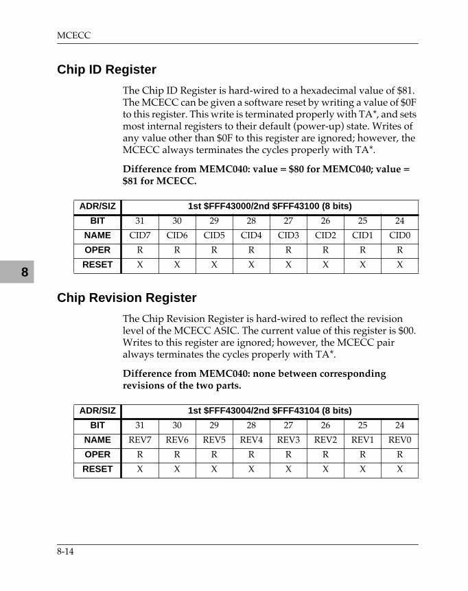
MCECC
8
Chip ID Register
The Chip ID Register is hard-wired to a hexadecimal value of $81. The MCECC can be given a software reset by writing a value of $0F to this register. This write is terminated properly with TA*, and sets most internal registers to their default (power-up) state. Writes of any value other than $0F to this register are ignored; however, the MCECC always terminates the cycles properly with TA*.
Difference from MEMC040: value = $80 for MEMC040; value = $81 for MCECC.
Chip Revision Register
The Chip Revision Register is hard-wired to reflect the revision level of the MCECC ASIC. The current value of this register is $00. Writes to this register are ignored; however, the MCECC pair always terminates the cycles properly with TA*.
Difference from MEMC040: none between corresponding revisions of the two parts.
ADR/SIZ 1st $FFF43000/2nd $FFF43100 (8 bits)
BIT 31 30 29 28 27 26 25 24
NAME CID7 CID6 CID5 CID4 CID3 CID2 CID1 CID0
OPER R R R R R R R R
RESET X X X X X X X X
ADR/SIZ 1st $FFF43004/2nd $FFF43104 (8 bits)
BIT 31 30 29 28 27 26 25 24
NAME REV7 REV6 REV5 REV4 REV3 REV2 REV1 REV0
OPER R R R R R R R R
RESET X X X X X X X X
8-14
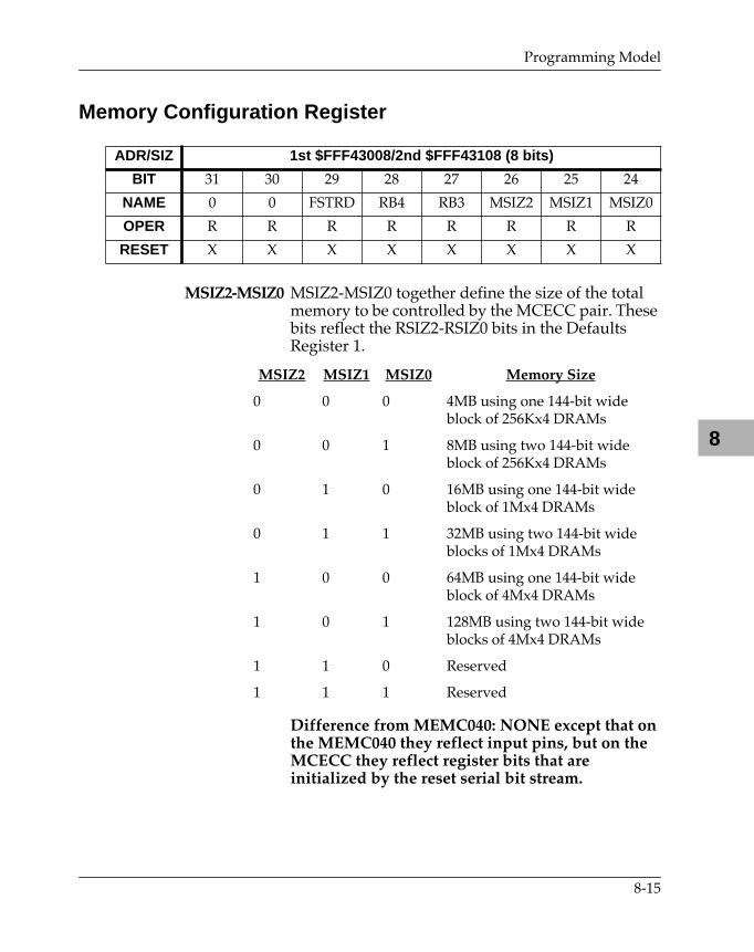
Programming Model
8
Memory Configuration Register
MSIZ2-MSIZ0 MSIZ2-MSIZ0 together define the size of the total memory to be controlled by the MCECC pair. These bits reflect the RSIZ2-RSIZ0 bits in the Defaults Register 1.
Difference from MEMC040: NONE except that on the MEMC040 they reflect input pins, but on the MCECC they reflect register bits that are initialized by the reset serial bit stream.
ADR/SIZ 1st $FFF43008/2nd $FFF43108 (8 bits)
BIT 31 30 29 28 27 26 25 24
NAME 0 0 FSTRD RB4 RB3 MSIZ2 MSIZ1 MSIZ0
OPER R R R R R R R R
RESET X X X X X X X X
MSIZ2 MSIZ1 MSIZ0 Memory Size
0 0 0 4MB using one 144-bit wide block of 256Kx4 DRAMs
0 0 1 8MB using two 144-bit wide block of 256Kx4 DRAMs
0 1 0 16MB using one 144-bit wide block of 1Mx4 DRAMs
0 1 1 32MB using two 144-bit wide blocks of 1Mx4 DRAMs
1 0 0 64MB using one 144-bit wide block of 4Mx4 DRAMs
1 0 1 128MB using two 144-bit wide blocks of 4Mx4 DRAMs
1 1 0 Reserved
1 1 1 Reserved
8-15
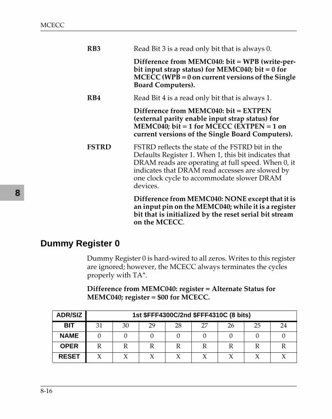
MCECC
8
RB3 Read Bit 3 is a read only bit that is always 0.
Difference from MEMC040: bit = WPB (write-per-bit input strap status) for MEMC040; bit = 0 for MCECC (WPB = 0 on current versions of the Single Board Computers).
RB4 Read Bit 4 is a read only bit that is always 1.
Difference from MEMC040: bit = EXTPEN (external parity enable input strap status) for MEMC040; bit = 1 for MCECC (EXTPEN = 1 on current versions of the Single Board Computers).
FSTRD FSTRD reflects the state of the FSTRD bit in the Defaults Register 1. When 1, this bit indicates that DRAM reads are operating at full speed. When 0, it indicates that DRAM read accesses are slowed by one clock cycle to accommodate slower DRAM devices.
Difference from MEMC040: NONE except that it is an input pin on the MEMC040; while it is a register bit that is initialized by the reset serial bit stream on the MCECC.
Dummy Register 0
Dummy Register 0 is hard-wired to all zeros. Writes to this register are ignored; however, the MCECC always terminates the cycles properly with TA*.
Difference from MEMC040: register = Alternate Status for MEMC040; register = $00 for MCECC.
ADR/SIZ 1st $FFF4300C/2nd $FFF4310C (8 bits)
BIT 31 30 29 28 27 26 25 24
NAME 0 0 0 0 0 0 0 0
OPER R R R R R R R R
RESET X X X X X X X X
8-16
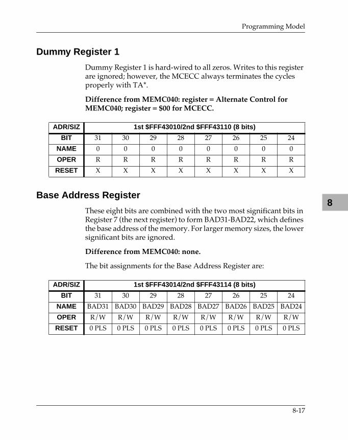
Programming Model
8
Dummy Register 1
Dummy Register 1 is hard-wired to all zeros. Writes to this register are ignored; however, the MCECC always terminates the cycles properly with TA*.
Difference from MEMC040: register = Alternate Control for MEMC040; register = $00 for MCECC.
Base Address Register
These eight bits are combined with the two most significant bits in Register 7 (the next register) to form BAD31-BAD22, which defines the base address of the memory. For larger memory sizes, the lower significant bits are ignored.
Difference from MEMC040: none.
The bit assignments for the Base Address Register are:
ADR/SIZ 1st $FFF43010/2nd $FFF43110 (8 bits)
BIT 31 30 29 28 27 26 25 24
NAME 0 0 0 0 0 0 0 0
OPER R R R R R R R R
RESET X X X X X X X X
ADR/SIZ 1st $FFF43014/2nd $FFF43114 (8 bits)
BIT 31 30 29 28 27 26 25 24
NAME BAD31 BAD30 BAD29 BAD28 BAD27 BAD26 BAD25 BAD24
OPER R/W R/W R/W R/W R/W R/W R/W R/W
RESET 0 PLS 0 PLS 0 PLS 0 PLS 0 PLS 0 PLS 0 PLS 0 PLS
8-17
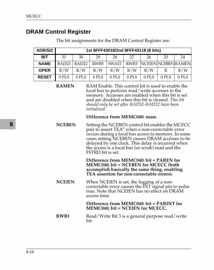
MCECC
8
DRAM Control RegisterThe bit assignments for the DRAM Control Register are:
RAMEN RAM Enable. This control bit is used to enable the local bus to perform read/write accesses to the memory. Accesses are enabled when this bit is set and are disabled when this bit is cleared. This bit should only be set after BAD31-BAD22 have been initialized.
Difference from MEMC040: none.
NCEBEN Setting the NCEBEN control bit enables the MCECC pair to assert TEA* when a non-correctable error occurs during a local bus access to memory. In some cases setting NCEBEN causes DRAM accesses to be delayed by one clock. This delay is incurred when the access is a local bus (or scrub) read and the FSTRD bit is set.
Difference from MEMC040: bit = PAREN for MEMC040; bit = NCEBEN for MCECC (both accomplish basically the same thing, enabling TEA assertion for non-correctable errors).
NCEIEN When NCEIEN is set, the logging of a non-correctable error causes the INT signal pin to pulse true. Note that NCEIEN has no effect on DRAM access time.
Difference from MEMC040: bit = PARINT for MEMC040; bit = NCEIEN for MCECC.
RWB3 Read/Write Bit 3 is a general purpose read/write bit.
ADR/SIZ 1st $FFF43018/2nd $FFF43118 (8 bits)
BIT 31 30 29 28 27 26 25 24
NAME BAD23 BAD22 RWB5 SWAIT RWB3 NCEIEN NCEBEN RAMEN
OPER R/W R/W R/W R/W R/W R/W R R/W
RESET 0 PLS 0 PLS 0 PLS 0 PLS 0 PLS 0 PLS 0 PLS 0 PLS
8-18
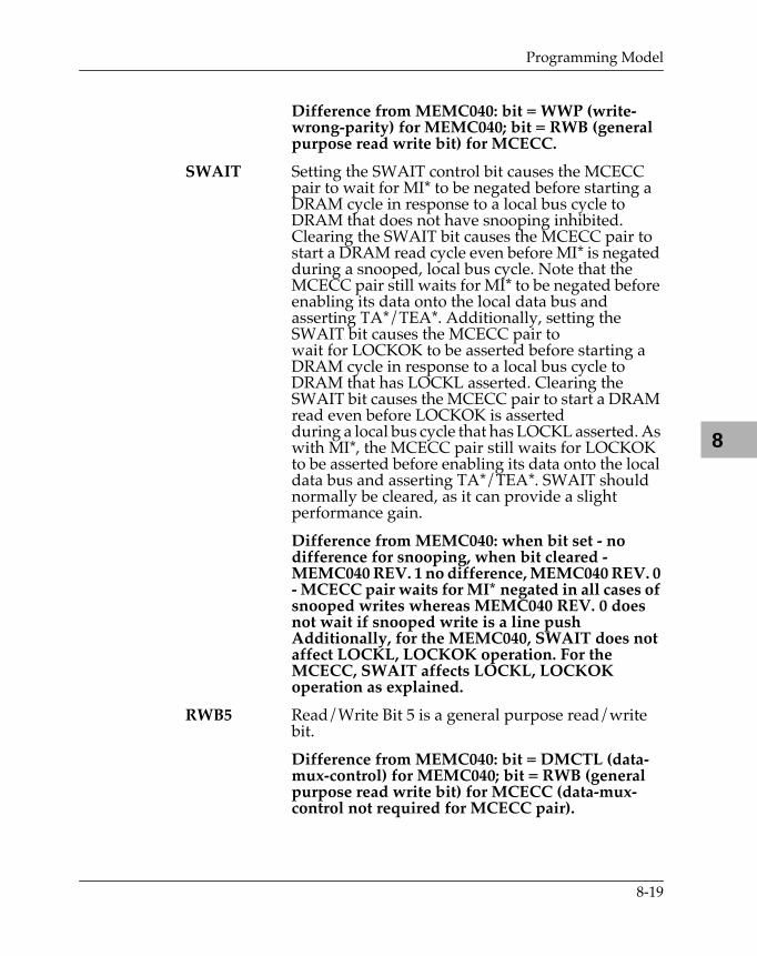
Programming Model
8
Difference from MEMC040: bit = WWP (write-wrong-parity) for MEMC040; bit = RWB (general purpose read write bit) for MCECC.
SWAIT Setting the SWAIT control bit causes the MCECC pair to wait for MI* to be negated before starting a DRAM cycle in response to a local bus cycle to DRAM that does not have snooping inhibited. Clearing the SWAIT bit causes the MCECC pair to start a DRAM read cycle even before MI* is negated during a snooped, local bus cycle. Note that the MCECC pair still waits for MI* to be negated before enabling its data onto the local data bus and asserting TA*/TEA*. Additionally, setting the SWAIT bit causes the MCECC pair towait for LOCKOK to be asserted before starting a DRAM cycle in response to a local bus cycle to DRAM that has LOCKL asserted. Clearing the SWAIT bit causes the MCECC pair to start a DRAM read even before LOCKOK is assertedduring a local bus cycle that has LOCKL asserted. As with MI*, the MCECC pair still waits for LOCKOK to be asserted before enabling its data onto the local data bus and asserting TA*/TEA*. SWAIT should normally be cleared, as it can provide a slight performance gain.
Difference from MEMC040: when bit set - no difference for snooping, when bit cleared - MEMC040 REV. 1 no difference, MEMC040 REV. 0 - MCECC pair waits for MI* negated in all cases of snooped writes whereas MEMC040 REV. 0 does not wait if snooped write is a line push Additionally, for the MEMC040, SWAIT does not affect LOCKL, LOCKOK operation. For the MCECC, SWAIT affects LOCKL, LOCKOK operation as explained.
RWB5 Read/Write Bit 5 is a general purpose read/write bit.
Difference from MEMC040: bit = DMCTL (data-mux-control) for MEMC040; bit = RWB (general purpose read write bit) for MCECC (data-mux-control not required for MCECC pair).
8-19
MCECC
8
BAD22, BAD23 These are the lower two bits of the DRAM base address described in the previous register.
Difference from MEMC040: none.
BCLK Frequency Register
The Bus Clock (BCLK) Frequency Register should be programmed with the hexadecimal value of the operating clock frequency in MHz (i.e., $19 for 25 MHz and $21 for 33 MHz). The MCECC pair uses the value programmed in this register to control the Prescaler Counter. The Prescaler Counter increments to $FF and then it is loaded with the two's compliment of the value in the BCLK Frequency Register. This produces a 1 MHz clock that is used by the refresh timer and the scrubber. When the BCLK Frequency Register is correctly programmed with the BCLK frequency, the DRAMs are refreshed approximately once every 15.6 microseconds. After power-up, this register is initialized to $19 (for 25 MHz).
Difference from MEMC040: none.
Note This register is configured only during power-up reset and is unchanged by software reset or local reset.
ADR/SIZ 1st $FFF4301C/2nd $FFF4311C (8 bits)
BIT 31 30 29 28 27 26 25 24
NAME BCK7 BCK6 BCK5 BCK4 BCK3 BCK2 BCK1 BCK0
OPER R/W R/W R/W R/W R/W R/W R/W R/W
RESET 0 P 0 P 0 P 1 P 1 P 0 P 0 P 1 P
8-20
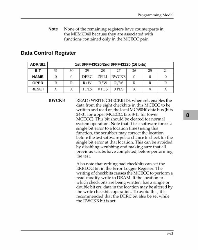
Programming Model
8
Note None of the remaining registers have counterparts in the MEMC040 because they are associated with functions contained only in the MCECC pair.
Data Control Register
RWCKB READ/WRITE CHECKBITS, when set, enables the data from the eight checkbits in this MCECC to be written and read on the local MC68040 data bus (bits 24-31 for upper MCECC, bits 8-15 for lower MCECC). This bit should be cleared for normal system operation. Note that if test software forces a single bit error to a location (line) using this function, the scrubber may correct the location before the test software gets a chance to check for the single bit error at that location. This can be avoided by disabling scrubbing and making sure that all previous scrubs have completed, before performing the test.
Also note that writing bad checkbits can set the ERRLOG bit in the Error Logger Register. The writing of checkbits causes the MCECC to perform a read-modify-write to DRAM. If the location to which check bits are being written, has a single or double bit err, data in the location may be altered by the write checkbits operation. To avoid this, it is recommended that the DERC bit also be set while the RWCKB bit is set.
ADR/SIZ 1st $FFF43020/2nd $FFF43120 (16 bits)
BIT 31 30 29 28 27 26 25 24
NAME 0 0 DERC ZFILL RWCKB 0 0 0
OPER R R R/W R/W R/W R R R
RESET X X 1 PLS 0 PLS 0 PLS X X X
8-21
MCECC
8
A suggested sequence for performing read-write checkbits is as follows:
1. Stop all scrub operations by clearing all of the STON bits and setting all of the STOFF bits in the Scrub Time On/Time Off Register.
2. Set the DERC and RWCKB bits in the Data Control Register.
3. Perform the desired read and/or write checkbit operations.
4. Clear the DERC and RWCKB bits in the Data Control Register.
5. Perform the desired testing related to the location/locations that have had their checkbits altered.
6. Allow the scrubber to proceed by restoring the STON and STOFF bits to their original state.
ZFILL ZERO FILL memory, when set, forces all zeros to be written to the DRAM during any kind of write cycle or scrub cycle. It is intended to be used with the zero-fill function. Refer to the section on Initialization at the end of this chapter. This bit should be cleared for normal system operation.
DERC DISABLE ERROR CORRECTION, when set to one, disables the MCECC from correcting single bit errors. Specifically, read data is presented to the local MC68040 data bus unaltered from the DRAM array. Less-than-line write data performs a read-modify-write without correcting single bit errors that may occur on the read portion of the read-modify-write. Note that DERC does not affect the generation of check bits. DERC should be cleared during normal system operation. DERC also allows the write portion of a read-modify-write to happen regardless of whether or not there is a multiple bit error during the read portion of the read-modify-write. DERC also affects scrub cycles.
8-22
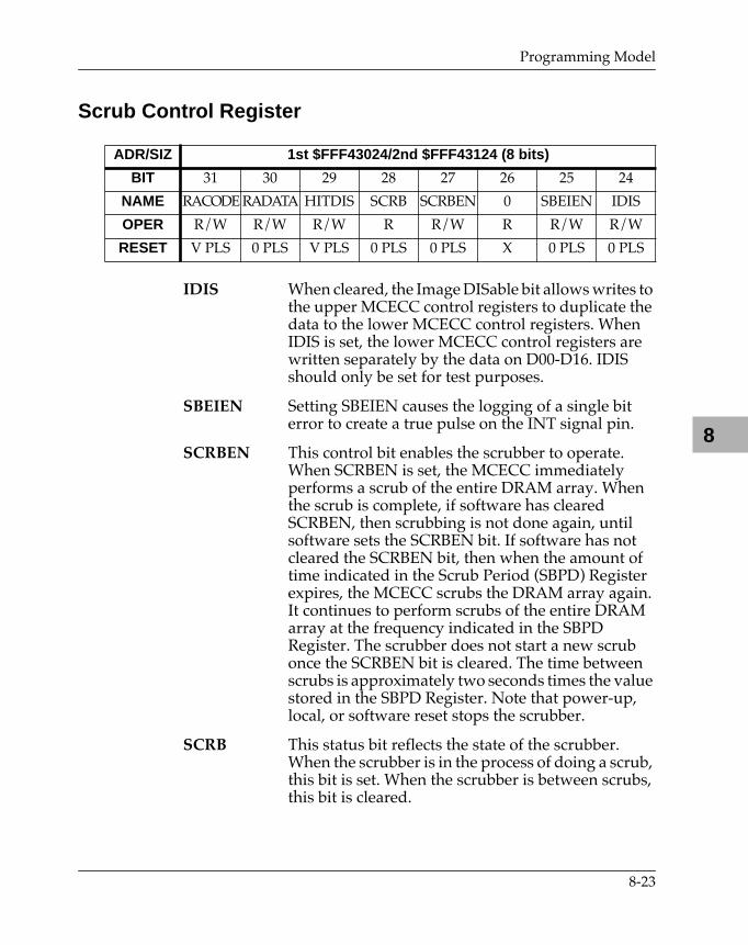
Programming Model
8
Scrub Control Register
IDIS When cleared, the Image DISable bit allows writes to the upper MCECC control registers to duplicate the data to the lower MCECC control registers. When IDIS is set, the lower MCECC control registers are written separately by the data on D00-D16. IDIS should only be set for test purposes.
SBEIEN Setting SBEIEN causes the logging of a single bit error to create a true pulse on the INT signal pin.
SCRBEN This control bit enables the scrubber to operate. When SCRBEN is set, the MCECC immediately performs a scrub of the entire DRAM array. When the scrub is complete, if software has cleared SCRBEN, then scrubbing is not done again, until software sets the SCRBEN bit. If software has not cleared the SCRBEN bit, then when the amount of time indicated in the Scrub Period (SBPD) Register expires, the MCECC scrubs the DRAM array again. It continues to perform scrubs of the entire DRAM array at the frequency indicated in the SBPD Register. The scrubber does not start a new scrub once the SCRBEN bit is cleared. The time between scrubs is approximately two seconds times the value stored in the SBPD Register. Note that power-up, local, or software reset stops the scrubber.
SCRB This status bit reflects the state of the scrubber. When the scrubber is in the process of doing a scrub, this bit is set. When the scrubber is between scrubs, this bit is cleared.
ADR/SIZ 1st $FFF43024/2nd $FFF43124 (8 bits)
BIT 31 30 29 28 27 26 25 24
NAME RACODE RADATA HITDIS SCRB SCRBEN 0 SBEIEN IDIS
OPER R/W R/W R/W R R/W R R/W R/W
RESET V PLS 0 PLS V PLS 0 PLS 0 PLS X 0 PLS 0 PLS
8-23
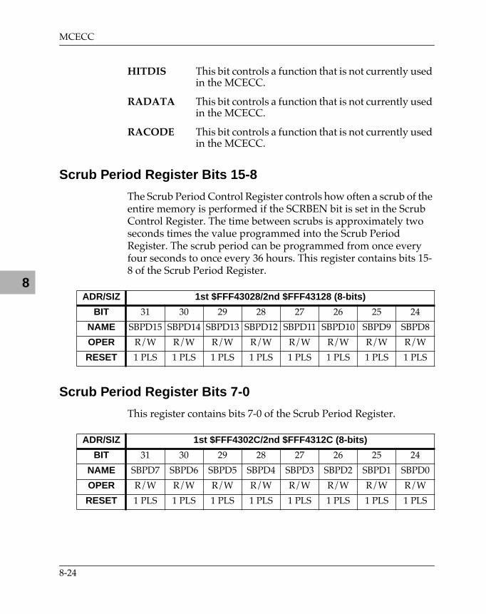
MCECC
8
HITDIS This bit controls a function that is not currently used in the MCECC.
RADATA This bit controls a function that is not currently used in the MCECC.
RACODE This bit controls a function that is not currently used in the MCECC.
Scrub Period Register Bits 15-8
The Scrub Period Control Register controls how often a scrub of the entire memory is performed if the SCRBEN bit is set in the Scrub Control Register. The time between scrubs is approximately two seconds times the value programmed into the Scrub Period Register. The scrub period can be programmed from once every four seconds to once every 36 hours. This register contains bits 15-8 of the Scrub Period Register.
Scrub Period Register Bits 7-0
This register contains bits 7-0 of the Scrub Period Register.
ADR/SIZ 1st $FFF43028/2nd $FFF43128 (8-bits)
BIT 31 30 29 28 27 26 25 24
NAME SBPD15 SBPD14 SBPD13 SBPD12 SBPD11 SBPD10 SBPD9 SBPD8
OPER R/W R/W R/W R/W R/W R/W R/W R/W
RESET 1 PLS 1 PLS 1 PLS 1 PLS 1 PLS 1 PLS 1 PLS 1 PLS
ADR/SIZ 1st $FFF4302C/2nd $FFF4312C (8-bits)
BIT 31 30 29 28 27 26 25 24
NAME SBPD7 SBPD6 SBPD5 SBPD4 SBPD3 SBPD2 SBPD1 SBPD0
OPER R/W R/W R/W R/W R/W R/W R/W R/W
RESET 1 PLS 1 PLS 1 PLS 1 PLS 1 PLS 1 PLS 1 PLS 1 PLS
8-24
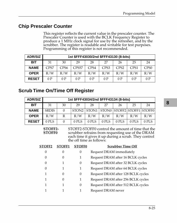
Programming Model
8
Chip Prescaler CounterThis register reflects the current value in the prescaler counter. The Prescaler Counter is used with the BCLK Frequency Register to produce a 1 MHz clock signal for use by the refresher, and by the scrubber. The register is readable and writable for test purposes. Programming of this register is not recommended.
Scrub Time On/Time Off Register
STOFF2- STOFF2-STOFF0 control the amount of time that theSTOFF0 scrubber refrains from requesting use of the DRAM
each time it gives it up during a scrub. They control the off time as follows:
ADR/SIZ 1st $FFF43030/2nd $FFF43130 (8-bits)
BIT 31 30 29 28 27 26 25 24
NAME CPS7 CPS6 CPS57 CPS4 CPS3 CPS2 CPS1 CPS0
OPER R/W R/W R/W R/W R/W R/W R/W R/W
RESET 0 P 0 P 0 P 0 P 0 P 0 P 0 P 0 P
ADR/SIZ 1st $FFF43034/2nd $FFF43134 (8-bits)
BIT 31 30 29 28 27 26 25 24
NAME SRDIS 0 STON2 STON1 STON0 STOFF2 STOFF1 STOFF0
OPER R/W R R/W R/W R/W R/W R/W R/W
RESET 0 PLS 0 0 PLS 0 PLS 0 PLS 0 PLS 0 PLS 0 PLS
STOFF2 STOFF1 STOFF0 Scrubber Time Off
0 0 0 Request DRAM immediately
0 0 1 Request DRAM after 16 BCLK cycles
0 1 0 Request DRAM after 32 BCLK cycles
0 1 1 Request DRAM after 64 BCLK cycles
1 0 0 Request DRAM after 128 BCLK cycles
1 0 1 Request DRAM after 256 BCLK cycles
1 1 0 Request DRAM after 512 BCLK cycles
1 1 1 Request DRAM never
8-25
MCECC
8
STON2- STON2-STON0 control the amount of time that theSTON0 scrubber occupies the DRAM before providing a
window during which the local bus and refresher might use it. They control the on time as follows:
Note that if STON2-0 is zero, the scrubber always releases the DRAM after one memory cycle, even if neither the local bus nor refresher need it.
SRDIS SRDIS disables the scrubber from performing reads during scrub cycles. This mode should only be used when using the scrub function to perform zero fill of the DRAM. Setting this bit causes the zero fill to happen faster. This bit should not be changed while scrubbing is in process.
STON2 STON1 STON0 Scrubber Time On
0 0 0 Keep DRAM for 1 memory cycle
0 0 1 Keep DRAM for 16 BCLK cycles
0 1 0 Keep DRAM for 32 BCLK cycles
0 1 1 Keep DRAM for 64 BCLK cycles
1 0 0 Keep DRAM for 128 BCLK cycles
1 0 1 Keep DRAM for 256 BCLK cycles
1 1 0 Keep DRAM for 512 BCLK cycles
1 1 1 Keep DRAM for TOTAL SCRUB TIME
8-26
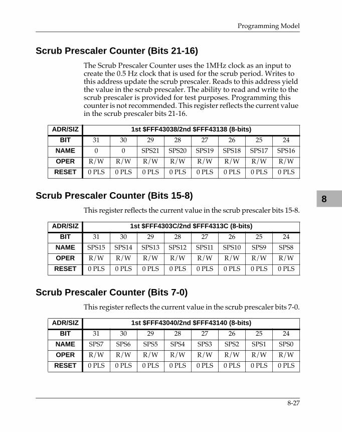
Programming Model
8
Scrub Prescaler Counter (Bits 21-16)
The Scrub Prescaler Counter uses the 1MHz clock as an input to create the 0.5 Hz clock that is used for the scrub period. Writes to this address update the scrub prescaler. Reads to this address yield the value in the scrub prescaler. The ability to read and write to the scrub prescaler is provided for test purposes. Programming this counter is not recommended. This register reflects the current value in the scrub prescaler bits 21-16.
Scrub Prescaler Counter (Bits 15-8)
This register reflects the current value in the scrub prescaler bits 15-8.
Scrub Prescaler Counter (Bits 7-0)
This register reflects the current value in the scrub prescaler bits 7-0.
ADR/SIZ 1st $FFF43038/2nd $FFF43138 (8-bits)
BIT 31 30 29 28 27 26 25 24
NAME 0 0 SPS21 SPS20 SPS19 SPS18 SPS17 SPS16
OPER R/W R/W R/W R/W R/W R/W R/W R/W
RESET 0 PLS 0 PLS 0 PLS 0 PLS 0 PLS 0 PLS 0 PLS 0 PLS
ADR/SIZ 1st $FFF4303C/2nd $FFF4313C (8-bits)
BIT 31 30 29 28 27 26 25 24
NAME SPS15 SPS14 SPS13 SPS12 SPS11 SPS10 SPS9 SPS8
OPER R/W R/W R/W R/W R/W R/W R/W R/W
RESET 0 PLS 0 PLS 0 PLS 0 PLS 0 PLS 0 PLS 0 PLS 0 PLS
ADR/SIZ 1st $FFF43040/2nd $FFF43140 (8-bits)
BIT 31 30 29 28 27 26 25 24
NAME SPS7 SPS6 SPS5 SPS4 SPS3 SPS2 SPS1 SPS0
OPER R/W R/W R/W R/W R/W R/W R/W R/W
RESET 0 PLS 0 PLS 0 PLS 0 PLS 0 PLS 0 PLS 0 PLS 0 PLS
8-27
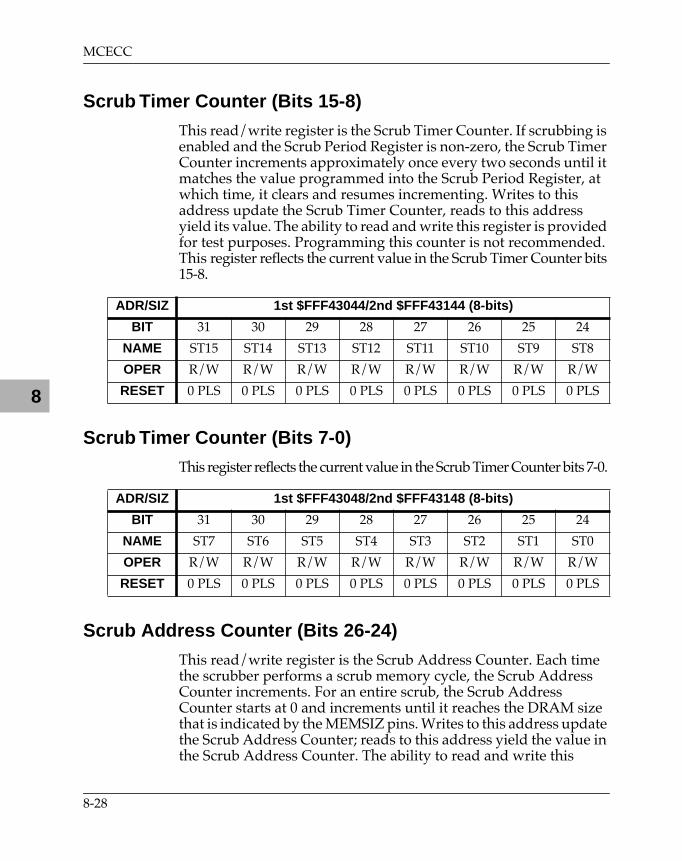
MCECC
8
Scrub Timer Counter (Bits 15-8)
This read/write register is the Scrub Timer Counter. If scrubbing is enabled and the Scrub Period Register is non-zero, the Scrub Timer Counter increments approximately once every two seconds until it matches the value programmed into the Scrub Period Register, at which time, it clears and resumes incrementing. Writes to this address update the Scrub Timer Counter, reads to this address yield its value. The ability to read and write this register is provided for test purposes. Programming this counter is not recommended. This register reflects the current value in the Scrub Timer Counter bits 15-8.
Scrub Timer Counter (Bits 7-0)
This register reflects the current value in the Scrub Timer Counter bits 7-0.
Scrub Address Counter (Bits 26-24)
This read/write register is the Scrub Address Counter. Each time the scrubber performs a scrub memory cycle, the Scrub Address Counter increments. For an entire scrub, the Scrub Address Counter starts at 0 and increments until it reaches the DRAM size that is indicated by the MEMSIZ pins. Writes to this address update the Scrub Address Counter; reads to this address yield the value in the Scrub Address Counter. The ability to read and write this
ADR/SIZ 1st $FFF43044/2nd $FFF43144 (8-bits)
BIT 31 30 29 28 27 26 25 24
NAME ST15 ST14 ST13 ST12 ST11 ST10 ST9 ST8
OPER R/W R/W R/W R/W R/W R/W R/W R/W
RESET 0 PLS 0 PLS 0 PLS 0 PLS 0 PLS 0 PLS 0 PLS 0 PLS
ADR/SIZ 1st $FFF43048/2nd $FFF43148 (8-bits)
BIT 31 30 29 28 27 26 25 24
NAME ST7 ST6 ST5 ST4 ST3 ST2 ST1 ST0
OPER R/W R/W R/W R/W R/W R/W R/W R/W
RESET 0 PLS 0 PLS 0 PLS 0 PLS 0 PLS 0 PLS 0 PLS 0 PLS
8-28
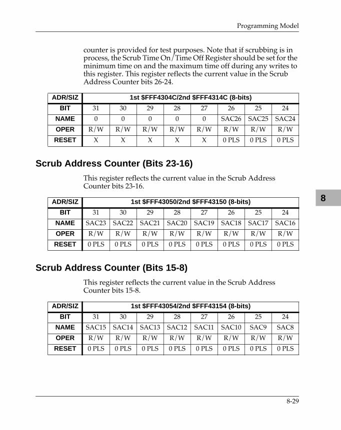
Programming Model
8
counter is provided for test purposes. Note that if scrubbing is in process, the Scrub Time On/Time Off Register should be set for the minimum time on and the maximum time off during any writes to this register. This register reflects the current value in the Scrub Address Counter bits 26-24.
Scrub Address Counter (Bits 23-16)
This register reflects the current value in the Scrub Address Counter bits 23-16.
Scrub Address Counter (Bits 15-8)
This register reflects the current value in the Scrub Address Counter bits 15-8.
ADR/SIZ 1st $FFF4304C/2nd $FFF4314C (8-bits)
BIT 31 30 29 28 27 26 25 24
NAME 0 0 0 0 0 SAC26 SAC25 SAC24
OPER R/W R/W R/W R/W R/W R/W R/W R/W
RESET X X X X X 0 PLS 0 PLS 0 PLS
ADR/SIZ 1st $FFF43050/2nd $FFF43150 (8-bits)
BIT 31 30 29 28 27 26 25 24
NAME SAC23 SAC22 SAC21 SAC20 SAC19 SAC18 SAC17 SAC16
OPER R/W R/W R/W R/W R/W R/W R/W R/W
RESET 0 PLS 0 PLS 0 PLS 0 PLS 0 PLS 0 PLS 0 PLS 0 PLS
ADR/SIZ 1st $FFF43054/2nd $FFF43154 (8-bits)
BIT 31 30 29 28 27 26 25 24
NAME SAC15 SAC14 SAC13 SAC12 SAC11 SAC10 SAC9 SAC8
OPER R/W R/W R/W R/W R/W R/W R/W R/W
RESET 0 PLS 0 PLS 0 PLS 0 PLS 0 PLS 0 PLS 0 PLS 0 PLS
8-29
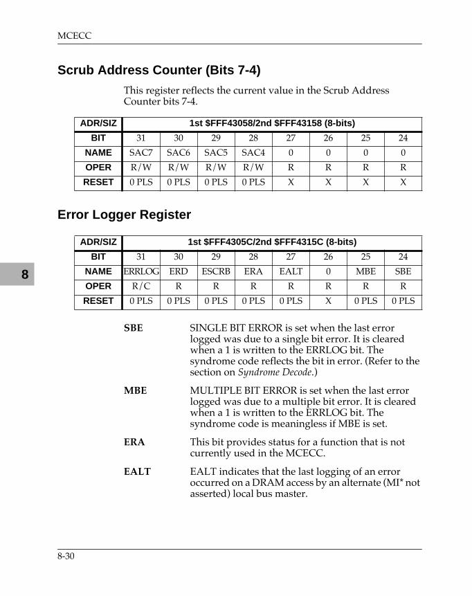
MCECC
8
Scrub Address Counter (Bits 7-4)
This register reflects the current value in the Scrub Address Counter bits 7-4.
Error Logger Register
SBE SINGLE BIT ERROR is set when the last error logged was due to a single bit error. It is cleared when a 1 is written to the ERRLOG bit. The syndrome code reflects the bit in error. (Refer to the section on Syndrome Decode.)
MBE MULTIPLE BIT ERROR is set when the last error logged was due to a multiple bit error. It is cleared when a 1 is written to the ERRLOG bit. The syndrome code is meaningless if MBE is set.
ERA This bit provides status for a function that is not currently used in the MCECC.
EALT EALT indicates that the last logging of an error occurred on a DRAM access by an alternate (MI* not asserted) local bus master.
ADR/SIZ 1st $FFF43058/2nd $FFF43158 (8-bits)
BIT 31 30 29 28 27 26 25 24
NAME SAC7 SAC6 SAC5 SAC4 0 0 0 0
OPER R/W R/W R/W R/W R R R R
RESET 0 PLS 0 PLS 0 PLS 0 PLS X X X X
ADR/SIZ 1st $FFF4305C/2nd $FFF4315C (8-bits)
BIT 31 30 29 28 27 26 25 24
NAME ERRLOG ERD ESCRB ERA EALT 0 MBE SBE
OPER R/C R R R R R R R
RESET 0 PLS 0 PLS 0 PLS 0 PLS 0 PLS X 0 PLS 0 PLS
8-30
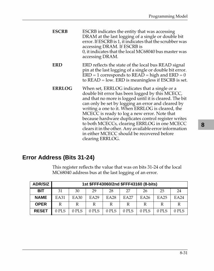
Programming Model
8
ESCRB ESCRB indicates the entity that was accessing DRAM at the last logging of a single or double bit error. If ESCRB is 1, it indicates that the scrubber was accessing DRAM. If ESCRB is0, it indicates that the local MC68040 bus master was accessing DRAM.
ERD ERD reflects the state of the local bus READ signal pin at the last logging of a single or double bit error. ERD = 1 corresponds to READ = high and ERD = 0 to READ = low. ERD is meaningless if ESCRB is set.
ERRLOG When set, ERRLOG indicates that a single or a double bit error has been logged by this MCECC, and that no more is logged until it is cleared. The bit can only be set by logging an error and cleared by writing a one to it. When ERRLOG is cleared, the MCECC is ready to log a new error. Note that because hardware duplicates control register writes to both MCECCs, clearing ERRLOG in one MCECC clears it in the other. Any available error information in either MCECC should be recovered before clearing ERRLOG.
Error Address (Bits 31-24)
This register reflects the value that was on bits 31-24 of the local MC68040 address bus at the last logging of an error.
ADR/SIZ 1st $FFF43060/2nd $FFF43160 (8-bits)
BIT 31 30 29 28 27 26 25 24
NAME EA31 EA30 EA29 EA28 EA27 EA26 EA25 EA24
OPER R R R R R R R R
RESET 0 PLS 0 PLS 0 PLS 0 PLS 0 PLS 0 PLS 0 PLS 0 PLS
8-31
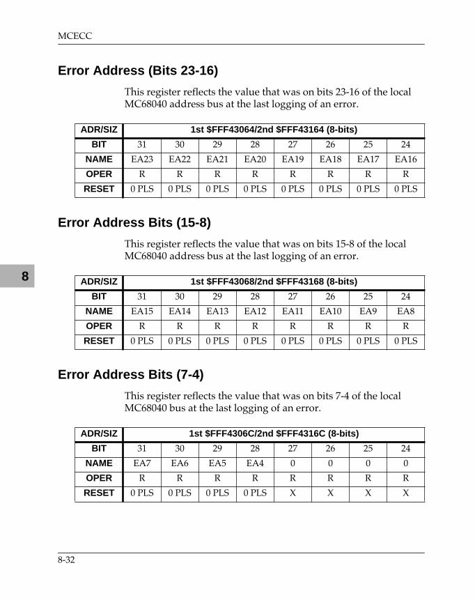
MCECC
8
Error Address (Bits 23-16)
This register reflects the value that was on bits 23-16 of the local MC68040 address bus at the last logging of an error.
Error Address Bits (15-8)
This register reflects the value that was on bits 15-8 of the local MC68040 address bus at the last logging of an error.
Error Address Bits (7-4)
This register reflects the value that was on bits 7-4 of the local MC68040 bus at the last logging of an error.
ADR/SIZ 1st $FFF43064/2nd $FFF43164 (8-bits)
BIT 31 30 29 28 27 26 25 24
NAME EA23 EA22 EA21 EA20 EA19 EA18 EA17 EA16
OPER R R R R R R R R
RESET 0 PLS 0 PLS 0 PLS 0 PLS 0 PLS 0 PLS 0 PLS 0 PLS
ADR/SIZ 1st $FFF43068/2nd $FFF43168 (8-bits)
BIT 31 30 29 28 27 26 25 24
NAME EA15 EA14 EA13 EA12 EA11 EA10 EA9 EA8
OPER R R R R R R R R
RESET 0 PLS 0 PLS 0 PLS 0 PLS 0 PLS 0 PLS 0 PLS 0 PLS
ADR/SIZ 1st $FFF4306C/2nd $FFF4316C (8-bits)
BIT 31 30 29 28 27 26 25 24
NAME EA7 EA6 EA5 EA4 0 0 0 0
OPER R R R R R R R R
RESET 0 PLS 0 PLS 0 PLS 0 PLS X X X X
8-32
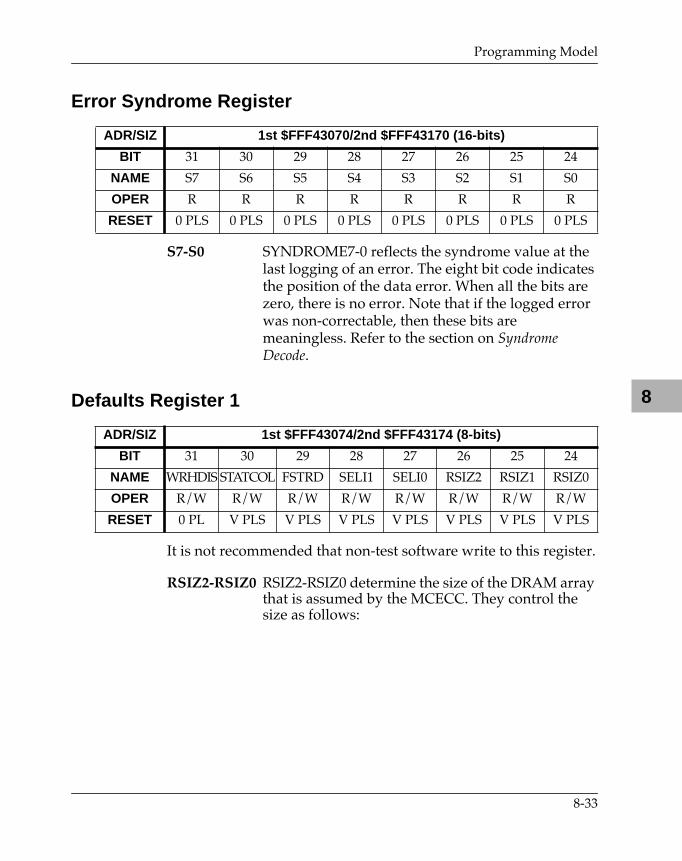
Programming Model
8
Error Syndrome Register
S7-S0 SYNDROME7-0 reflects the syndrome value at the last logging of an error. The eight bit code indicates the position of the data error. When all the bits are zero, there is no error. Note that if the logged error was non-correctable, then these bits are meaningless. Refer to the section on Syndrome Decode.
Defaults Register 1
It is not recommended that non-test software write to this register.
RSIZ2-RSIZ0 RSIZ2-RSIZ0 determine the size of the DRAM array that is assumed by the MCECC. They control the size as follows:
ADR/SIZ 1st $FFF43070/2nd $FFF43170 (16-bits)
BIT 31 30 29 28 27 26 25 24
NAME S7 S6 S5 S4 S3 S2 S1 S0
OPER R R R R R R R R
RESET 0 PLS 0 PLS 0 PLS 0 PLS 0 PLS 0 PLS 0 PLS 0 PLS
ADR/SIZ 1st $FFF43074/2nd $FFF43174 (8-bits)
BIT 31 30 29 28 27 26 25 24
NAME WRHDIS STATCOL FSTRD SELI1 SELI0 RSIZ2 RSIZ1 RSIZ0
OPER R/W R/W R/W R/W R/W R/W R/W R/W
RESET 0 PL V PLS V PLS V PLS V PLS V PLS V PLS V PLS
8-33
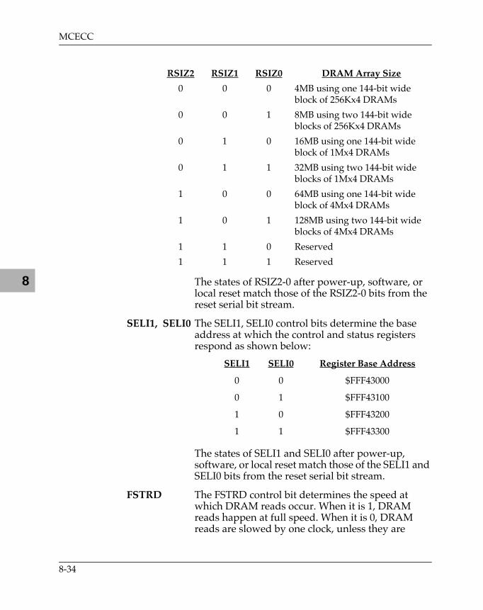
MCECC
8
The states of RSIZ2-0 after power-up, software, or local reset match those of the RSIZ2-0 bits from the reset serial bit stream.SELI1, SELI0 The SELI1, SELI0 control bits determine the base address at which the control and status registers respond as shown below:
The states of SELI1 and SELI0 after power-up, software, or local reset match those of the SELI1 and SELI0 bits from the reset serial bit stream.
FSTRD The FSTRD control bit determines the speed at which DRAM reads occur. When it is 1, DRAM reads happen at full speed. When it is 0, DRAM reads are slowed by one clock, unless they are
RSIZ2 RSIZ1 RSIZ0 DRAM Array Size
0 0 0 4MB using one 144-bit wide block of 256Kx4 DRAMs
0 0 1 8MB using two 144-bit wide blocks of 256Kx4 DRAMs
0 1 0 16MB using one 144-bit wide block of 1Mx4 DRAMs
0 1 1 32MB using two 144-bit wide blocks of 1Mx4 DRAMs
1 0 0 64MB using one 144-bit wide block of 4Mx4 DRAMs
1 0 1 128MB using two 144-bit wide blocks of 4Mx4 DRAMs
1 1 0 Reserved
1 1 1 Reserved
SELI1 SELI0 Register Base Address
0 0 $FFF43000
0 1 $FFF43100
1 0 $FFF43200
1 1 $FFF43300
8-34
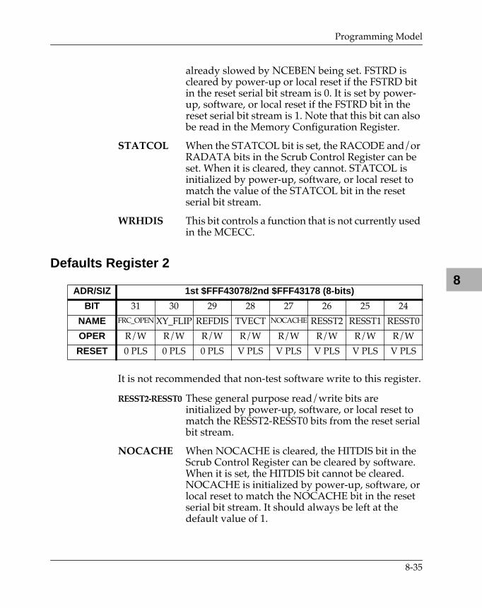
Programming Model
8
already slowed by NCEBEN being set. FSTRD is cleared by power-up or local reset if the FSTRD bit in the reset serial bit stream is 0. It is set by power-up, software, or local reset if the FSTRD bit in the reset serial bit stream is 1. Note that this bit can also be read in the Memory Configuration Register.
STATCOL When the STATCOL bit is set, the RACODE and/or RADATA bits in the Scrub Control Register can be set. When it is cleared, they cannot. STATCOL is initialized by power-up, software, or local reset to match the value of the STATCOL bit in the reset serial bit stream.
WRHDIS This bit controls a function that is not currently used in the MCECC.
Defaults Register 2
It is not recommended that non-test software write to this register.
RESST2-RESST0 These general purpose read/write bits are initialized by power-up, software, or local reset to match the RESST2-RESST0 bits from the reset serial bit stream.
NOCACHE When NOCACHE is cleared, the HITDIS bit in the Scrub Control Register can be cleared by software. When it is set, the HITDIS bit cannot be cleared. NOCACHE is initialized by power-up, software, or local reset to match the NOCACHE bit in the reset serial bit stream. It should always be left at the default value of 1.
ADR/SIZ 1st $FFF43078/2nd $FFF43178 (8-bits)
BIT 31 30 29 28 27 26 25 24
NAME FRC_OPEN XY_FLIP REFDIS TVECT NOCACHE RESST2 RESST1 RESST0
OPER R/W R/W R/W R/W R/W R/W R/W R/W
RESET 0 PLS 0 PLS 0 PLS V PLS V PLS V PLS V PLS V PLS
8-35
MCECC
8
TVECT TVECT makes bidirectional signals work while running the vendors test vectors on this chip. It should be cleared for normal operation. It is initialized by power-up, software, or local reset to match the TVECT bit from the reset serial bit stream.
REFDIS When REFDIS is set, refreshing is disabled. This mode should only be used for testing, as DRAM must have refresh to operate correctly. REFDIS is initialized by power-up, software, or local reset to match the REFDIS bit in the reset serial bit stream.
XY_FLIP When XY_FLIP is set, the opposite internal set of cache latches is selected. This bit should be used with caution and is for test vector coverage improvement.
FRC_OPN When FRC_OPN is set, the internal DRAM read latches are forced continuously open. This bit should be used with caution and is for test vector coverage improvement.
Initialization
Most DRAM vendors require that the DRAMs be subjected to some number of access cycles before the DRAMs are fully operational. The MCECC does not perform this automatically but depends on software to perform enough dummy accesses to DRAM to meet the requirement. The number of required cycles is less than 10. If there are multiple blocks of DRAM, software has to perform at least 10 accesses to each block.
The MCECC pair provides a fast zero fill capability. The sequence shown below performs such a zero fill. It zeros all of the DRAM controlled by this MCECC pair at the rate of 100 MB/second when the BCLK pin is operating at 25 MHz. This sequence may have to be altered to perform the scrub more slowly if the scrub causes the DRAM to consume too much power at full speed.
8-36
Programming Model
8
1. Make sure that the scrubber is disabled by clearing the SCRBEN bit in the Scrub Control Register. (Clear bit 27 of offset $24.)
2. Make sure that the scrubber is done with any old scrub cycles by waiting for the SCRB bit in the Scrub Control Register to be cleared. (Wait for bit 28 of offset $24 = 0.)
3. Discontinue all accesses from the MC68040 bus to the DRAM.
4. Ensure that all accesses have stopped by clearing the RAMEN bit in the DRAM Control Register. (Clear bit 0 of offset $18)
5. Set the ZFILL bit in the MCECC pair. (Set Bit 28 of offset $20)
6. Set the Scrub Time On/Time Off Register for the maximum rate and to do write cycles, by setting the SRDIS bit, setting all of the STON bits, and clearing all of the STOFF bits. (Write $B8 to offset $34)
7. Enable scrubbing by setting the SCRBEN bit in the Scrub Control Register. (Set bit 27 of offset $24.)
8. Ensure that the zero-fill has started by waiting for the SCRB bit in the Scrub Control Register to be set. (Wait for bit 28 of offset $24 = 1.)
9. Ensure that the zero-fill stops after one time through, by clearing the SCRBEN bit in the Scrub Control Register. (Clear bit 27 of offset $24.)
10. Wait for the zero-fill to complete by waiting for the SCRB bit in the Scrub Control Register to be cleared. (Wait for bit 28 of offset $24 = 0.)
11. Clear the ZFILL bit in the MCECC pair. (Clear Bit 28 of offset $20)
12. The entire DRAM that is controlled by this MCECC is now zero-filled. The software can now program the appropriate scrubbing mode and other desired initialization, and enable DRAM for operation.
8-37
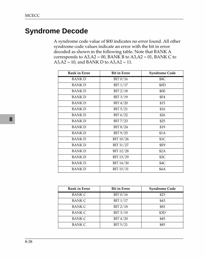
MCECC
8
Syndrome DecodeA syndrome code value of $00 indicates no error found. All other syndrome code values indicate an error with the bit in error decoded as shown in the following table. Note that BANK A corresponds to A3,A2 = 00, BANK B to A3,A2 = 01, BANK C to A3,A2 = 10, and BANK D to A3,A2 = 11.
Bank in Error Bit in Error Syndrome Code
BANK D BIT 0/16 $8C
BANK D BIT 1/17 $0D
BANK D BIT 2/18 $0E
BANK D BIT 3/19 $F4
BANK D BIT 4/20 $15
BANK D BIT 5/21 $16
BANK D BIT 6/22 $26
BANK D BIT 7/23 $25
BANK D BIT 8/24 $19
BANK D BIT 9/25 $1A
BANK D BIT 10/26 $1C
BANK D BIT 11/27 $E9
BANK D BIT 12/28 $2A
BANK D BIT 13/29 $2C
BANK D BIT 14/30 $4C
BANK D BIT 15/31 $4A
Bank in Error Bit in Error Syndrome Code
BANK C BIT 0/16 $23
BANK C BIT 1/17 $43
BANK C BIT 2/18 $83
BANK C BIT 3/19 $3D
BANK C BIT 4/20 $45
BANK C BIT 5/21 $85
8-38
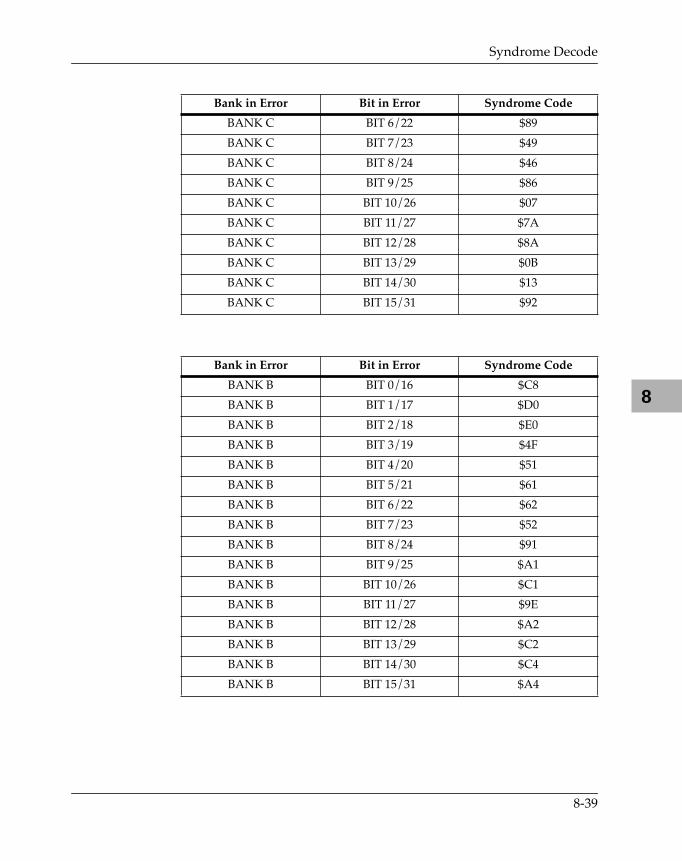
Syndrome Decode
8
BANK C BIT 6/22 $89
BANK C BIT 7/23 $49
BANK C BIT 8/24 $46
BANK C BIT 9/25 $86
BANK C BIT 10/26 $07
BANK C BIT 11/27 $7A
BANK C BIT 12/28 $8A
BANK C BIT 13/29 $0B
BANK C BIT 14/30 $13
BANK C BIT 15/31 $92
Bank in Error Bit in Error Syndrome Code
BANK B BIT 0/16 $C8
BANK B BIT 1/17 $D0
BANK B BIT 2/18 $E0
BANK B BIT 3/19 $4F
BANK B BIT 4/20 $51
BANK B BIT 5/21 $61
BANK B BIT 6/22 $62
BANK B BIT 7/23 $52
BANK B BIT 8/24 $91
BANK B BIT 9/25 $A1
BANK B BIT 10/26 $C1
BANK B BIT 11/27 $9E
BANK B BIT 12/28 $A2
BANK B BIT 13/29 $C2
BANK B BIT 14/30 $C4
BANK B BIT 15/31 $A4
Bank in Error Bit in Error Syndrome Code
8-39
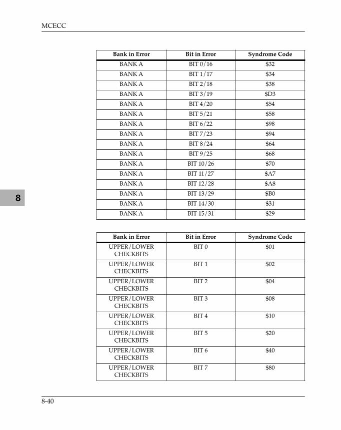
MCECC
8
Bank in Error Bit in Error Syndrome Code
BANK A BIT 0/16 $32
BANK A BIT 1/17 $34
BANK A BIT 2/18 $38
BANK A BIT 3/19 $D3
BANK A BIT 4/20 $54
BANK A BIT 5/21 $58
BANK A BIT 6/22 $98
BANK A BIT 7/23 $94
BANK A BIT 8/24 $64
BANK A BIT 9/25 $68
BANK A BIT 10/26 $70
BANK A BIT 11/27 $A7
BANK A BIT 12/28 $A8
BANK A BIT 13/29 $B0
BANK A BIT 14/30 $31
BANK A BIT 15/31 $29
Bank in Error Bit in Error Syndrome Code
UPPER/LOWER CHECKBITS
BIT 0 $01
UPPER/LOWER CHECKBITS
BIT 1 $02
UPPER/LOWER CHECKBITS
BIT 2 $04
UPPER/LOWER CHECKBITS
BIT 3 $08
UPPER/LOWER CHECKBITS
BIT 4 $10
UPPER/LOWER CHECKBITS
BIT 5 $20
UPPER/LOWER CHECKBITS
BIT 6 $40
UPPER/LOWER CHECKBITS
BIT 7 $80
8-40
9
9Printer and Serial PortConnectionsIntroductionThis chapter has connection diagrams for the printer port and the four serial ports on the MVME167/177/187, and or the serial ports on the MVME166/176. These ports are connected to external devices through the MVME712 series of transition modules.
The configuration of the serial ports as Data Terminal Equipment (DTE) or Data Circuit-terminating Equipment (DCE) is accomplished by jumpers on the transition modules. For more information, refer to the userÕs manual for your MVME712 series transition board.
Connection DiagramsThe MVME712x transition module connection diagrams are shown in the following figures:
Figure Number
Name
9-1 MVME167/177/187 Printer Port with MVME712A 9-2 MVME167/177/187 Printer Port with MVME712M 9-3 MVME167/177/187 Serial Port 1 ConÞgured as DCE 9-4 MVME167/177/187 Serial Port 2 ConÞgured as DCE 9-5 MVME167/177/187 Serial Port 3 ConÞgured as DCE 9-6 MVME167/177/187 Serial Port 4 ConÞgured as DCE 9-7 MVME167/177/187 Serial Port 1 ConÞgured as DTE 9-8 MVME167/177/187 Serial Port 2 ConÞgured as DTE 9-9 MVME167/177/187 Serial Port 3 ConÞgured as DTE 9-10 MVME167/177/187 Serial Port 4 ConÞgured as DTE 9-11 MVME167/177/187 Serial Port 1 with MVME712A 9-12 MVME167/177/187 Serial Port 2 with MVME712A
9-1
Printer and Serial Port Connections
9
9-13 MVME167/177/187 Serial Port 3 with MVME712A 9-14 MVME167/177/187 Serial Port 4 with MVME712A 9-15 MVME166/176 Serial Ports with MVME712-10
(Sheets 1 through 4) 9-16 MVME166/176 Serial Ports with MVME712-06
(Sheets 1 through 3)
Figure Number
Name
9-2
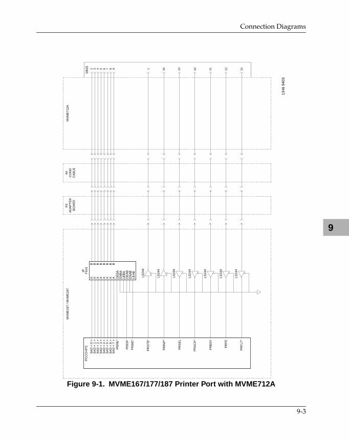
Connection Diagrams
9
Figure 9-1. MVME167/177/187 Printer Port with MVME712A
1346
940
3
MV
ME
167
/ MV
ME
187
LS24
4
EN
BA
LEB
AO
EA
BE
NA
BLE
AB
EN
BA
OE
BA
A A A A A A A A
SA
D <
0 >
SA
D <
1 >
SA
D <
2 >
SA
D <
3 >
SA
D <
4 >
SA
D <
5 >
SA
D <
6 >
SA
D <
7 >
B B B B B B B B
LS24
4
LS24
4
LS24
4
LS24
4
LS24
4
LS24
4
2 3 4 5 6 7 8 9 1 16 13 10 11 12 15
PC
CC
HIP
2IP
F54
3
PR
RE
*
PD
EN
*
PR
WE
*
PR
ST
B*
PR
INP
*
PR
SE
L
PR
AC
K*
PR
BS
Y
PR
PE
PR
FLT
*
P2
AD
AP
TE
RB
OA
RD
64C
ON
DC
AB
LE
MV
ME
712A
DB
25
9-3
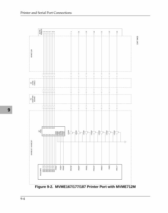
Printer and Serial Port Connections
9
Figure 9-2. MVME167/177/187 Printer Port with MVME712M
1347
940
3
MV
ME
167
/ MV
ME
187
LS24
4
EN
BA
LEB
AO
EA
BE
NA
BLE
AB
EN
BA
OE
BA
A A A A A A A A
SA
D <
0 >
SA
D <
1 >
SA
D <
2 >
SA
D <
3 >
SA
D <
4 >
SA
D <
5 >
SA
D <
6 >
SA
D <
7 >
B B B B B B B B
LS24
4
LS24
4
LS24
4
LS24
4
LS24
4
LS24
4
2 3 4 5 6 7 8 9 1 31 13 10 11 12 32
PC
CC
HIP
29P F54
3
PR
RE
*
PD
EN
*
PR
WE
*
PR
ST
B*
PR
INP
*
PR
SE
L
PR
AC
K*
PR
BS
Y
PR
PE
PR
FLT
*
P2
AD
AP
TE
RB
OA
RD
64C
ON
DC
AB
LE
MV
ME
712M
36 P
INR
IBB
ON
9-4

Connection Diagrams
9
Figure 9-3. MVME167/177/187 Serial Port 1 Configured as DCE
1348
940
3
MV
ME
167
/ MV
ME
187
P2
AD
AP
TE
RB
OA
RD
64C
ON
DC
AB
LE
DB
25C
D24
01 DT
R0*
RX
D0
CD
0*
CT
S0*
TX
D0
34 85 54
1.5K
MC
1454
06
D D
MC
1454
06
C23
C25
MC
1454
06
MC
1454
06
C24
C26
5539
R R
MV
ME
712
TR
AN
SIT
ION
BO
AR
D
1.5K
1.5K
+12
V
+12
V
3 8 5 6 7 2 4
RX
D
DC
D
CT
S
DS
R
GN
D
TX
D
RT
S
9-5
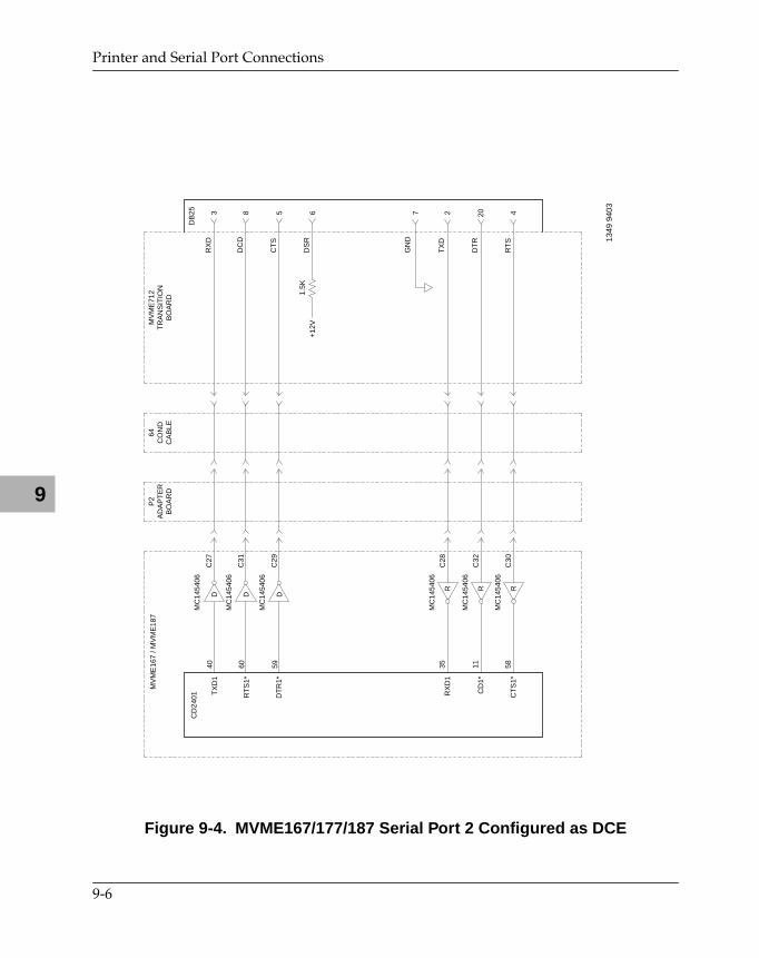
Printer and Serial Port Connections
9
Figure 9-4. MVME167/177/187 Serial Port 2 Configured as DCE
MC
1454
06
DC
2740
3R
XD
MC
1454
06
DC
3160
8D
CD
MC
1454
06
DC
2959
5C
TS 13
49 9
403
MV
ME
167
/ MV
ME
187
P2
AD
AP
TE
RB
OA
RD
64C
ON
DC
AB
LE
DB
25C
D24
01 RX
D1
35M
C14
5406
C28
R
MV
ME
712
TR
AN
SIT
ION
BO
AR
D
1.5K
+12
V6 7 2 4
DS
R
GN
D
TX
D
RT
S
CD
1*11
MC
1454
06C
32R
20D
TR
CT
S1*
58M
C14
5406
C30
R
DT
R1*
RT
S1*
TX
D1
9-6

Connection Diagrams
9
Figure 9-5. MVME167/177/187 Serial Port 3 Configured as DCE
MC
1454
06
DA
1941
3R
XD
MC
1454
06
DA
2365
8D
CD
MC
1454
06
DA
2164
5C
TS 13
50 9
403
MV
ME
167
/ MV
ME
187
P2
AD
AP
TE
RB
OA
RD
64C
ON
DC
AB
LE
DB
25C
D24
01 RX
D2
36M
C14
5406
A20
R
MV
ME
712
TR
AN
SIT
ION
BO
AR
D
1.5K
+12
V6 7 2 4
DS
R
GN
D
TX
D
RT
S
CD
2*18
MC
1454
06A
24R
20D
TR
CT
S2*
63M
C14
5406
A22
R
DT
R2*
RT
S2*
TX
D2
9-7
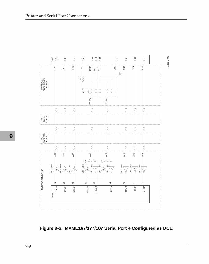
Printer and Serial Port Connections
9
Figure 9-6. MVME167/177/187 Serial Port 4 Configured as DCE
MC
1454
06
DA
2542
3R
XD
MC
1454
06
DA
3069
8D
CD
MC
1454
06
DA
2768
5C
TS 13
51 9
403
MV
ME
167
/ MV
ME
187
P2
AD
AP
TE
RB
OA
RD
64C
ON
DC
AB
LE
DB
25C
D24
01 RX
D3
38M
C14
5406
A26
R
MV
ME
712
TR
AN
SIT
ION
BO
AR
D
1.5K
+12
V6 7 2 4
DS
R
GN
D
TX
D
RT
S
CD
3*22
MC
1454
06
A31
R20
DT
R
CT
S3*
67M
C14
5406
A29
R
DT
R3*
RT
S3*
TX
D3
A32
15R
TX
C
A28
RR
XC
TT
XC
J15
1T
RX
C4
RT
XC
4
MC
1454
06
D D
R R
MC
1454
06
MC
1454
06
MC
1454
06
J6 J7
1 1
TX
CO
3
RX
CI3
TX
CI3
47 51 52
17 24
9-8

Connection Diagrams
9
Figure 9-7. MVME167/177/187 Serial Port 1 Configured as DTE
1352
940
3
MV
ME
167
/ MV
ME
187
P2
AD
AP
TE
RB
OA
RD
64C
ON
DC
AB
LE
DB
25C
D24
01 DT
R0*
RX
D0
CD
0*
CT
S0*
TX
D0
34 85 54
1.5K
MC
1454
06
D D
MC
1454
06
C23
C25
MC
1454
06
MC
1454
06
C24
C26
5539
R R
MV
ME
712
TR
AN
SIT
ION
BO
AR
D
1.5K
+12
V
2 20 4 7 3 5
TX
D
DT
R
RT
S
GN
D
RX
D
CT
S
9P
9-9

Printer and Serial Port Connections
9
Figure 9-8. MVME167/177/187 Serial Port 2 Configured as DTE
MC
1454
06
DC
2740
2T
XD
MC
1454
06
DC
3160
20D
TR
MC
1454
06
DC
2959
4R
TS 13
53 9
403
MV
ME
167
/ MV
ME
187
P2
AD
AP
TE
RB
OA
RD
64C
ON
DC
AB
LE
DB
25C
D24
01 RX
D1
35M
C14
5406
C28
R
MV
ME
712
TR
AN
SIT
ION
BO
AR
D
7 3 5
GN
D
RX
D
CT
S
CD
1*11
MC
1454
06C
32R
8D
CD
CT
S1*
58M
C14
5406
C30
R
DT
R1*
RT
S1*
TX
D1
11P
9-10
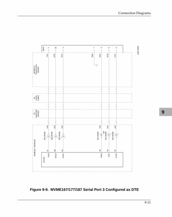
Connection Diagrams
9
Figure 9-9. MVME167/177/187 Serial Port 3 Configured as DTE
MC
1454
06
DA
1941
2T
XD
MC
1454
06
DA
2365
20D
TR
MC
1454
06
DA
2164
4R
TS 13
54 9
403
MV
ME
167
/ MV
ME
187
P2
AD
AP
TE
RB
OA
RD
64C
ON
DC
AB
LE
DB
25C
D24
01 RX
D2
36M
C14
5406
A20
R
MV
ME
712
TR
AN
SIT
ION
BO
AR
D
7 3 5
GN
D
RX
D
CT
S
CD
2*18
MC
1454
06A
24R
8D
CD
CT
S2*
63M
C14
5406
A22
R
DT
R2*
RT
S2*
TX
D2
9P
9-11
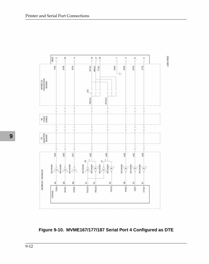
Printer and Serial Port Connections
9
Figure 9-10. MVME167/177/187 Serial Port 4 Configured as DTE
MC
1454
06
DA
2542
2T
XD
MC
1454
06
DA
3069
20D
TR
MC
1454
06
DA
2768
4R
TS 13
55 9
403
MV
ME
167
/ MV
ME
187
P2
AD
AP
TE
RB
OA
RD
64C
ON
DC
AB
LE
DB
25C
D24
01 RX
D3
38M
C14
5406
A26
R
MV
ME
712
TR
AN
SIT
ION
BO
AR
D
7 3 5
GN
D
RX
D
CT
S
CD
3*22
MC
1454
06
A31
R8
DC
D
CT
S3*
67M
C14
5406
A29
R
DT
R3*
RT
S3*
TX
D3
A32
15R
TX
C
A28
RR
XC
TT
XC
J15
1T
RX
C4
RT
XC
4
MC
1454
06
D D
R R
MC
1454
06
MC
1454
06
MC
1454
06
J6 J7
1 1
TX
CO
3
RX
CI3
TX
CI3
47 51 52
17 24
9-12
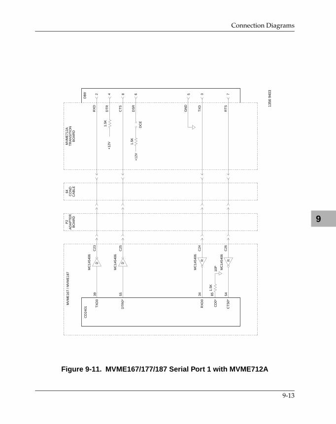
9Printer and Serial Port Connections
0Connection Diagrams
9
Connection Diagrams
Figure 9-11. MVME167/177/187 Serial Port 1 with MVME712A
1356
940
3
MV
ME
167
/ MV
ME
187
P2
AD
AP
TE
RB
OA
RD
64C
ON
DC
AB
LE
DB
9C
D24
01 DT
R0*
RX
D0
CD
0*
CT
S0*
TX
D0
34 85 54
1.5K
MC
1454
06
D D
MC
1454
06
C23
C25
MC
1454
06
MC
1454
06
C24
C26
5539
R R
MV
ME
712A
TR
AN
SIT
ION
BO
AR
D
1.5K
1.5K
+12
V
+12
V
2 4 8 6 5 3 7
RX
D
DT
R
CT
S
DS
R
GN
D
TX
D
RT
S
10P
DC
E
9-13

Printer and Serial Port Connections
9
Figure 9-12. MVME167/177/187 Serial Port 2 with MVME712A
MC
1454
06
DC
2740
2R
XD
MC
1454
06
DC
3160
1D
CD
MC
1454
06
DC
2959
8C
TS 13
5794
03
MV
ME
167
/ MV
ME
187
P2
AD
AP
TE
RB
OA
RD
64C
ON
DC
AB
LE
DB
9C
D24
01 RX
D1
35M
C14
5406
C28
R
MV
ME
712A
TR
AN
SIT
ION
BO
AR
D
5 3 7
GN
D
TX
D
RT
S
CD
1*11
MC
1454
06C
32R
4D
TR
CT
S1*
58M
C14
5406
C30
R
DT
R1*
RT
S1
TX
D1
13P
1.5K
+12
V6
DS
R
DC
E
9-14
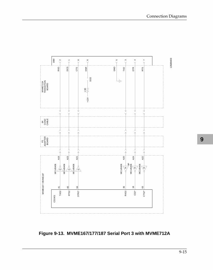
Connection Diagrams
9
Figure 9-13. MVME167/177/187 Serial Port 3 with MVME712A
MC
1454
06
DA
1941
2R
XD
MC
1454
06
DA
2365
1D
CD
MC
1454
06
DA
2164
8C
TS 13
5894
03
MV
ME
167
/ MV
ME
187
P2
AD
AP
TE
RB
OA
RD
64C
ON
DC
AB
LE
DB
9C
D24
01 RX
D2
36M
C14
5406
A20
R
MV
ME
712A
TR
AN
SIT
ION
BO
AR
D
5 3 7
GN
D
TX
D
RT
S
CD
2*18
MC
1454
06A
24R
4D
TR
CT
S2*
63M
C14
5406
A22
R
DT
R2*
RT
S2
TX
D2
9P
1.5K
+12
V6
DS
R
DC
E
9-15
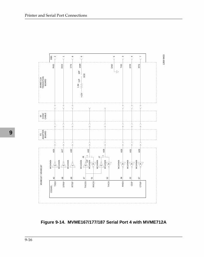
Printer and Serial Port Connections
9
Figure 9-14. MVME167/177/187 Serial Port 4 with MVME712A
MC
1454
06
DA
2542
2R
XD
MC
1454
06
DA
2768
1D
CD
MC
1454
06
DA
3069
8C
TS 13
59 9
403
MV
ME
167
/ MV
ME
187
P2
AD
AP
TE
RB
OA
RD
64C
ON
DC
AB
LE
DB
9C
D24
01 RX
D3
38M
C14
5406
A26
R
MV
ME
712A
TR
AN
SIT
ION
BO
AR
D
5 3 7
GN
D
TX
D
RT
S
CD
3*22
MC
1454
06
A31
R4
DT
R
CT
S3*
67M
C14
5406
A29
R
RT
S3*
DT
R3*
TX
D3
A32
A28
MC
1454
06
D D
R R
MC
1454
06
MC
1454
06
MC
1454
06
J6 J7
1 1
TX
CO
3
RX
CI3
TX
CI3
47 51 52
1.5K
+12
V6
DS
R
DC
E
11P
10P
13P
9-16
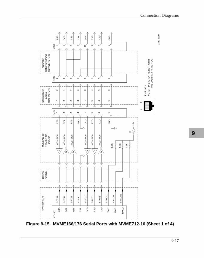
Connection Diagrams
9
Figure 9-15. MVME166/176 Serial Ports with MVME712-10 (Sheet 1 of 4)
1340
951
0
100-
PIN
MV
ME
712-
10
+5V
0
1.5K
1.5K
1.5K
CA
BLE
TR
AN
SIT
ION
BO
AR
D
CR
OS
SO
VE
RC
AB
LER
J45
TO
RJ4
5
AD
AP
TE
RD
TE
(T
ER
MIN
AL)
DE
VIC
E T
O R
J45
R
D D D
R R
MC
1454
06
MC
1454
06
MC
1454
06
MC
1454
06
MC
1454
06
MC
1454
06
CT
S
DT
R
RT
S
GN
D
DC
D
RX
D
TX
D
GN
D
7 8 2 3 1 5 4 6
7 8 2 3 1 5 4 6
2 1 7 6 8 4 5 3
2 1 7 6 8 4 5 3
4 8 5 6 20 2 3 7
RT
S
DC
D
CT
S
DS
R
DT
R
TX
D
RX
D
GN
D
18
RJ4
5 JA
CK
NO
TE
: P
IN 1
IS T
O T
HE
LE
FT
WIT
HT
HE
OP
EN
ING
FA
CIN
G Y
OU
RJ4
5R
J45
DB
25
CT
S
DT
R
RT
S
DS
R
DC
D
RX
D
TX
D
TX
CI
RX
CI
RX
CO
CD
2401
MV
ME
166/
176
SC
TS
1
SD
TR
1
SR
TS
1
SD
SR
1
SD
CD
1
SR
XD
1
ST
XD
1
ST
XC
I1
SR
XC
I1
SR
XC
O1
9-17
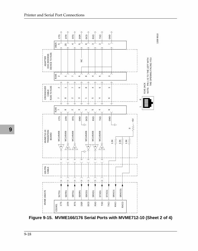
Printer and Serial Port Connections
9
Figure 9-15. MVME166/176 Serial Ports with MVME712-10 (Sheet 2 of 4)
1339
951
0
CT
S
DT
R
RT
S
DS
R
DC
D
RX
D
TX
D
TX
CI
RX
CI
RX
CO
CD
2401
MV
ME
166
/176
100-
PIN
MV
ME
712-
10
+5V
0
1.5K
1.5K
1.5K
CA
BLE
TR
AN
SIT
ION
BO
AR
D
CR
OS
SO
VE
RC
AB
LER
J45
TO
RJ4
5
AD
AP
TE
RD
CE
(M
OD
EM
)D
EV
ICE
TO
RJ4
5
R
D D D
R R
MC
1454
06
MC
1454
06
MC
1454
06
MC
1454
06
MC
1454
06
MC
1454
06
CT
S
DT
R
RT
S
GN
D
DC
D
RX
D
TX
D
GN
D
7 8 2 3 1 5 4 6
7 8 2 3 1 5 4 6
2 1 7 6 8 4 5 3
2 1 7 6 8 4 5 3
5 20 4 6 8 3 2 7
CT
S
DT
R
RT
S
DS
R
DC
D
RX
D
TX
D
GN
D
NC
18
RJ4
5 JA
CK
NO
TE
: P
IN 1
IS T
O T
HE
LE
FT
WIT
HT
HE
OP
EN
ING
FA
CIN
G Y
OU
RJ4
5R
J45
DB
25
SC
TS
1
SD
TR
1
SR
TS
1
SD
SR
1
SD
CD
1
SR
XD
1
ST
XD
1
ST
XC
I1
SR
XC
I1
SR
XC
O1
9-18
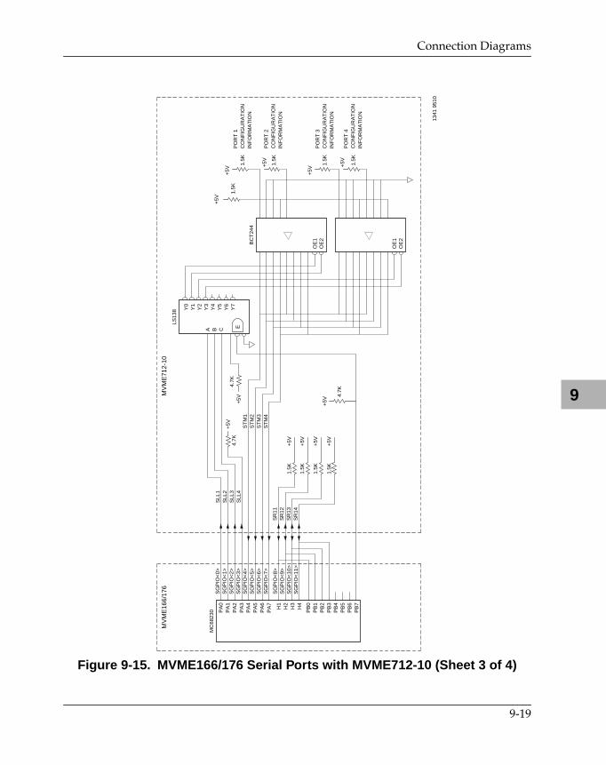
Connection Diagrams
9
Figure 9-15. MVME166/176 Serial Ports with MVME712-10 (Sheet 3 of 4)
1.5K
1.5K
1.5K
1.5K
PO
RT
1C
ON
FIG
UR
AT
ION
INF
OR
MA
TIO
N
PO
RT
2C
ON
FIG
UR
AT
ION
INF
OR
MA
TIO
N
PO
RT
3C
ON
FIG
UR
AT
ION
INF
OR
MA
TIO
N
PO
RT
4C
ON
FIG
UR
AT
ION
INF
OR
MA
TIO
N
+5V
+5V
+5V
+5V
+5V
1.5K
BC
T24
4
OE
1O
E2
Y0
Y1
Y2
Y3
Y4
Y5
Y6
Y7
E
LS13
8
A B C
4.7K
+5V
MV
ME
712-
10
4.7K
+5V
1.5K
1.5K
1.5K
1.5K
+5V
+5V
+5V
+5V
+5V
4.7K
ST
M1
ST
M2
ST
M3
ST
M4
SR
11S
R12
SR
13S
R14
MV
ME
166/
176
PA
0P
A1
PA
2P
A3
PA
4P
A5
PA
6P
A7
PB
0P
B1
PB
2P
B3
PB
4P
B5
PB
6P
B7
H1
H2
H3
H4
SG
PIO
<0>
SG
PIO
<1>
SG
PIO
<2>
SG
PIO
<3>
SG
PIO
<4>
SG
PIO
<5>
SG
PIO
<6>
SG
PIO
<7>
SG
PIO
<8>
SG
PIO
<9>
SG
PIO
<10
>S
GP
IO<
11>
MC
6823
0
OE
1O
E2
1341
951
0
SLL
1S
LL2
SLL
3S
LL4
9-19
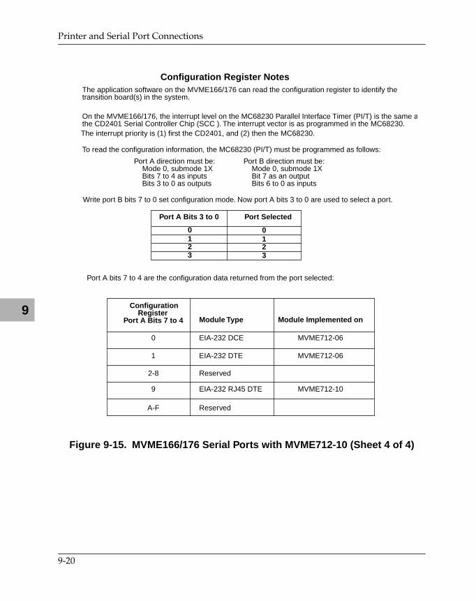
Printer and Serial Port Connections
9
Figure 9-15. MVME166/176 Serial Ports with MVME712-10 (Sheet 4 of 4)
Configuration Register NotesThe application software on the MVME166/176 can read the configuration register to identify the transition board(s) in the system.
On the MVME166/176, the interrupt level on the MC68230 Parallel Interface Timer (PI/T) is the same a
To read the configuration information, the MC68230 (PI/T) must be programmed as follows:
Port A direction must be: Mode 0, submode 1X Bits 7 to 4 as inputs Bits 3 to 0 as outputs
Port B direction must be: Mode 0, submode 1X Bit 7 as an output Bits 6 to 0 as inputs
Write port B bits 7 to 0 set configuration mode. Now port A bits 3 to 0 are used to select a port.
Port A Bits 3 to 0 Port Selected
0123
0123
Configuration RegisterPort A Bits 7 to 4 Module Type Module Implemented on
0
1
2-8
9
A-F
EIA-232 DCE
EIA-232 DTE
EIA-232 RJ45 DTE
Reserved
Reserved
MVME712-06
the CD2401 Serial Controller Chip (SCC ). The interrupt vector is as programmed in the MC68230.The interrupt priority is (1) first the CD2401, and (2) then the MC68230.
Port A bits 7 to 4 are the configuration data returned from the port selected:
MVME712-06
MVME712-10
9-20
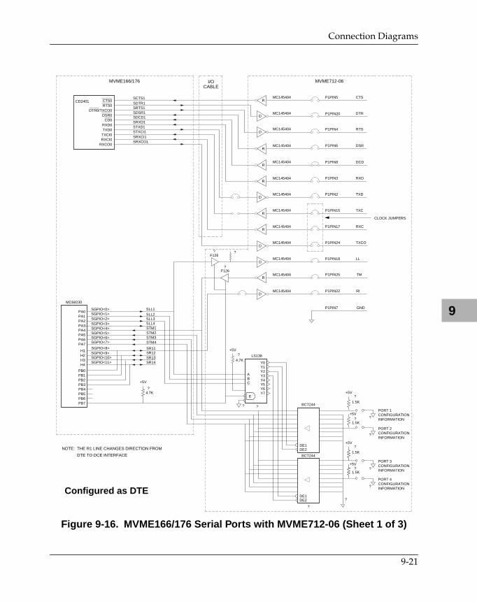
Connection Diagrams
9
Figure 9-16. MVME166/176 Serial Ports with MVME712-06 (Sheet 1 of 3)
P1PIN5
P1PIN20
P1PIN4
P1PIN2
P1PIN17
P1PIN24
P1PIN18
P1PIN22
P1PIN25
1.5K
PORT 1CONFIGURATIONINFORMATION
PORT 2CONFIGURATIONINFORMATION
PORT 3CONFIGURATIONINFORMATION
PORT 4CONFIGURATIONINFORMATION
+5V
BCT244
DE1DE2
Y0Y1Y2Y3Y4Y5Y6Y7
E
LS138
ABC
4.7K
+5V
SR11SR12SR13SR14
PA0PA1PA2PA3PA4PA5PA6PA7
PB0PB1PB2PB3PB4PB5PB6PB7
H1H2H3H4
SGPIO<0>SGPIO<1>SGPIO<2>SGPIO<3>SGPIO<4>SGPIO<5>SGPIO<6>SGPIO<7>
SGPIO<8>SGPIO<9>SGPIO<10>SGPIO<11>
MC68230
DE1DE2
SLL1SLL2SLL3SLL4STM1STM2STM3STM4
1.5K
+5V
1.5K
+5V
1.5K
+5V?
?
?
?
?
4.7K
+5V
?
? ?
?
?
?
?
?
?
BCT244
MVME166/176 MVME712-06
D
D
SCTS1SDTR1SRTS1SDSR1SDCD1SRXD1STXD1STXCI1
CTS0RTS0
DTR0/TXCO0DSR0
CD0RXD0TXD0TXCI0RXCI0
RXCO0
SRXCI1SRXCO1
CD2401
I/OCABLE
?F126
?
F126?
MC145404
MC145404
MC145404
MC145404
MC145404
MC145404
MC145404
MC145404
MC145404
MC145404
MC145404
CLOCK JUMPERS
CTS
DTR
RTS
RXD
TXD
RXC
TXCO
LL
RI
TM
P1PIN7 GND
NOTE: THE R1 LINE CHANGES DIRECTION FROM
DTE TO DCE INTERFACE
D
MC145404 P1PIN3
MC145404 P1PIN8
TXC
P1PIN6
D
R
R
R
R
D
D
R
R
R
DSR
DCD
P1PIN15
Configured as DTE
9-21
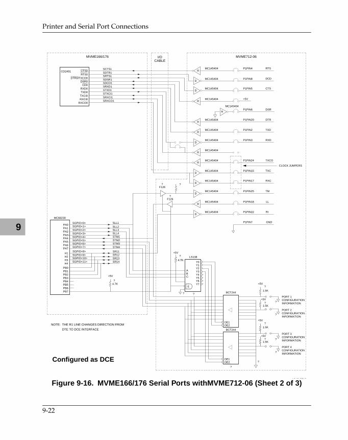
Printer and Serial Port Connections
9
Figure 9-16. MVME166/176 Serial Ports withMVME712-06 (Sheet 2 of 3)
P1PIN4
P1PIN8
P1PIN5
+5V
P1PIN6
P1PIN3
P1PIN24
P1PIN15
P1PIN17
P1PIN25
P1PIN22
P1PIN18
1.5K
PORT 1CONFIGURATIONINFORMATION
PORT 2CONFIGURATIONINFORMATION
PORT 3CONFIGURATIONINFORMATION
PORT 4CONFIGURATIONINFORMATION
+5V
BCT244
DE1DE2
Y0Y1Y2Y3Y4Y5Y6Y7
E
LS138
ABC
4.7K
+5V
SR11SR12SR13SR14
PA0PA1PA2PA3PA4PA5PA6PA7
PB0PB1PB2PB3PB4PB5PB6PB7
H1H2H3H4
SGPIO<0>SGPIO<1>SGPIO<2>SGPIO<3>SGPIO<4>SGPIO<5>SGPIO<6>SGPIO<7>
SGPIO<8>SGPIO<9>SGPIO<10>SGPIO<11>
MC68230
DE1DE2
1343 9510
SLL1SLL2SLL3SLL4STM1STM2STM3STM4
1.5K
+5V
1.5K
+5V
1.5K
+5V?
?
?
?
?
4.7K
+5V
?
? ?
?
?
?
?
?
?
BCT244
MVME166/176 MVME712-06
D
R
R
D
D
R
R
D
D
R
SCTS1SDTR1SRTS1SDSR1SDCD1SRXD1STXD1STXCI1
CTS0RTS0
DTR0/TXCO0DSR0
CD0RXD0TXD0TXCI0RXCI0
RXCO0
SRXCI1SRXCO1
CD2401
I/OCABLE
?F126
?
F126?
MC145404
MC145404
MC145404
MC145404
MC145404
MC145404
MC145404
MC145404
MC145404
MC145404
MC145404
MC145404
MC145404
CLOCK JUMPERS
RTS
DCD
CTS
DSR
TXD
RXD
TXCO
TXC
TM
RI
LL
P1PIN7 GND
NOTE: THE R1 LINE CHANGES DIRECTION FROM
DTE TO DCE INTERFACE
R
R
D
D
MC145404 P1PIN2
MC145404 P1PIN20 DTR
RXC
R
Configured as DCE
9-22
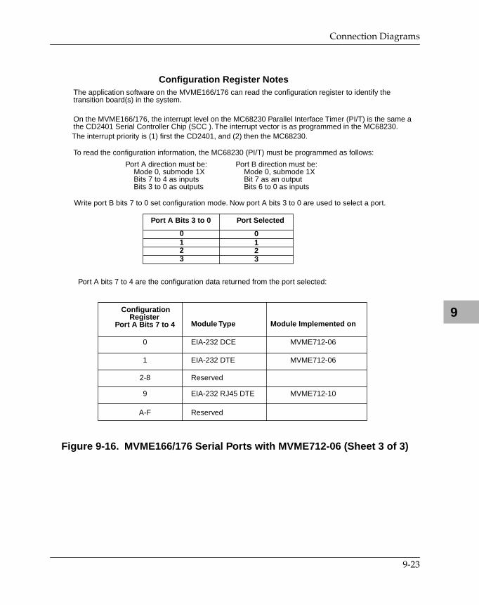
Connection Diagrams
9
Figure 9-16. MVME166/176 Serial Ports with MVME712-06 (Sheet 3 of 3)
Configuration Register NotesThe application software on the MVME166/176 can read the configuration register to identify the transition board(s) in the system.
On the MVME166/176, the interrupt level on the MC68230 Parallel Interface Timer (PI/T) is the same a
To read the configuration information, the MC68230 (PI/T) must be programmed as follows:
Port A direction must be: Mode 0, submode 1X Bits 7 to 4 as inputs Bits 3 to 0 as outputs
Port B direction must be: Mode 0, submode 1X Bit 7 as an output Bits 6 to 0 as inputs
Write port B bits 7 to 0 set configuration mode. Now port A bits 3 to 0 are used to select a port.
Port A Bits 3 to 0 Port Selected
0123
0123
Configuration RegisterPort A Bits 7 to 4 Module Type Module Implemented on
0
1
2-8
9
A-F
EIA-232 DCE
EIA-232 DTE
EIA-232 RJ45 DTE
Reserved
Reserved
MVME712-06
the CD2401 Serial Controller Chip (SCC ). The interrupt vector is as programmed in the MC68230.The interrupt priority is (1) first the CD2401, and (2) then the MC68230.
Port A bits 7 to 4 are the configuration data returned from the port selected:
MVME712-06
MVME712-10
9-23
Printer and Serial Port Connections
9
9-24
Index
Symbols+12 Vdc power 4-101
Numerics166BBug 1-6166Bug, execute 4-10453C710 1-13
SCSI I/O processor 6-7SCSI memory map 3-15
82596CA 1-12Ethernet LAN memory map 3-14LAN coprocessor 6-4LANC Interrupt Control Register 6-37
AA24 (standard) access cycles 4-34, 4-37A32 (extended) access cycles 4-35, 4-37abort interrupt 4-90ABORT switch 4-99
interrupt 4-80, 4-84, 4-89interrupter 4-19
access cycles, DRAM 8-36access time
ROMs 4-49SRAM 4-54
access timer 5-33VMEbus 4-7
accessing DRAM 8-31ACFAIL interrupt 4-91ACFAIL signal 4-99adder 4-33, 4-36adders, VMEchip2 4-27address latch/multiplexer (AMUX) 7-1address modifier codes 4-12, 4-43, 4-44, 4-45,
4-60Address Modifier Select Register 4-34, 4-36Address Offset Register
local bus to VSB map decoder 5-36, 5-39, 5-42, 5-45
VSB to local bus map decoder 5-61, 5-65address range
devices 3-2local bus to VSB map decoder 5-35, 5-38, 5-41,
5-44VSB to local bus map decoder 5-61, 5-65
Address Translation Address Register 4-30, 4-32, 4-42
Address Translation Select Register 4-31, 4-32, 4-43
addresses53C710 registers 3-1582596 registers 3-14BBRAM configuration area 3-17CD2401 registers 3-9GCSR 4-46location monitors 4-107MC68230 registers 3-13MCECC CSRs 8-9MK48T08 registers 3-16PCCchip2 6-13SCC status and control registers 6-29SCSI controller registers 3-15SRAM 4-20TOD clock 3-20VMEbus resources 4-37VMEchip2 LCSR 4-21VSB slots 5-13
alternate address space 5-63, 5-67Alternate Control Register 7-10Alternate Status Register 7-10AMUX 7-1Application-Specific Integrated Circuit
(ASIC) 1-1arbiter time-out timer 4-67arbitration
algorithm 4-17ID 5-32, 5-58MCECC 8-8mode 5-32mode, PRI 4-17timer time-out 5-24, 5-33timer, VSBchip2 5-16
IN-1
Index
INDEX
array size, DRAM 8-33assertion, definition viiasterisk (*) viAttribute Register 4-43, 4-44, 4-45, 5-62
snoop bits 4-28auto vector mode 6-9
BBack Off signal 6-6bank A,B ROM cycles 4-50base address
MC68230 1-10register 8-34
base address of memoryMCECC 8-17, 8-20MEMC040 7-10, 7-13
Base Address Register 7-10battery backup 1-6baud rates 1-9BBRAM 1-7, 6-2
interface, PCCchip2 6-3restoring lost Ethernet address 1-12speed 6-17
BBRAM Configuration Area memory map 3-17BBRAM/TOD clock memory map 3-16BBSY* time 4-105BCSR memory map 5-50BGIN filters 4-105bidirectional signals 8-36big-endian viibinary number viblock access cycles 4-34, 4-37block diagram
VMEchip2 4-5VSBchip2 5-4
block transfer cycles 4-12, 5-8, 5-12block transfer mode 4-61Board Control Register 4-73Board Control/Status Registers (BCSRs) 5-19,
5-50board failure 4-73board status/control register, VMEchip2 4-113BootBug 1-6bounce mode 5-9, 5-37, 5-40, 5-43, 5-46BRDFAIL signal 4-73burst cycles 7-2
burst read cycle type 8-5burst write cycle type 8-6Bus Clock (BCLK) Frequency Register 8-20Bus Clock Register 7-13bus error 6-5
processing 1-29sources 1-27status, SCSI 6-39VSB 5-24
bus requester, VMEchip2 4-8bus sizing 5-11bus timers 1-14, 4-17
example of use 1-24byte ordering viibyte, definition vii
Ccache coherency
MVME166/167 1-23MVME187 1-24
cache coherency, MCECC 8-3cache latches 8-36cache line (burst) cycles 8-2cache line cycles 7-2CD2401 1-8
interrupt priority 9-20, 9-23memory map 3-9SCC interface 6-8
chip arbiter 4-17Chip Control/Status Register 5-23chip defaults, MCECC 8-9Chip ID Register 7-7
MCECC 8-14MEMC040 7-7PCCchip2 6-16
Chip Prescaler Counter 8-25Chip Revision Register 6-16, 7-7
MCECC 8-14MEMC040 7-7
Chip Speed Register 6-48clear bits
LANC error 6-36SCC error 6-29SCSI error 6-39
clear MPU status bits 4-65clear overflow counter
IN-2
Index
INDEX
tick timer 1 6-25tick timer 2 6-24
clear-on-compare 4-71, 4-72tick timer 1 6-25tick timer 2 6-24
clock cycles 7-2clock prescaler 4-14, 4-70, 4-76, 5-35, 5-47clocks, local bus 4-49, 4-54command packet, DMAC 4-53configuration jumpers
MVME166 2-5MVME167 2-8MVME177 2-12MVME187 2-16
configuration register 9-19configuration register notes 9-20, 9-23configuring the MVME166 1-6connection diagrams
printer and serial port 9-1transition module 9-1
connectors, P1 and P2 2-2Control and Status Registers (CSRs)
MCECC 8-9PCCchip2 6-13VMEchip2 4-21VSBchip2 5-19
Control and Status Registers memory map, PCCchip2 6-14
control bit, definition viiconventions, manual vicounter enable
tick timer 1 6-25tick timer 2 6-24
counter, tick timer 1 4-71counter, tick timer 2 4-72CPU identifier (C040) 6-18cycle types, MCECC 8-4
DD16, D32 cycles 4-59D32, D64 block transfer cycles 4-61D64 block access cycles 4-34, 4-37daisy-chain, IACK 4-17data access cycles 4-34, 4-36data bus structure 1-2Data Control Register 8-21
data multiplexer (MEMMUX) 7-1data mux control 7-12data transfers 4-43, 4-44, 4-45, 4-46, 4-48, 4-59,
5-8DCE connections 9-1decimal number videcoders 3-5, 4-6, 4-10
enable 4-47local bus to VMEbus map 4-37map, VSBchip2 5-5, 5-9VMEchip2 4-26
default state 7-7Defaults Register 8-33defaults, MCECC chip 8-9description
MCECC 8-2MEMC040 7-2PCCchip2 6-2VMEchip2 4-4VSBchip2 5-3
device has bus 5-31device ready 5-53device wants bus 5-31DIN connectors 2-2direct mode 4-58, 6-9disable error correction 8-22DMA Control Register 4-54DMA controller
programming 4-52DMA Controller (DMAC) 4-11, 4-52DMAC
command table format 4-53done 4-66enable 4-58halt 4-58interrupt 4-81, 4-85, 4-89, 4-92interrupt counter 4-65interrupter 4-19LTO error 1-32offboard error 1-32parity error 1-31registers 4-53requester 4-57TEA, cause unidentified 1-32VMEbus Address Counter 4-62VMEbus error 1-31
IN-3
Index
INDEX
VMEbus requester 4-13DMAC Byte Counter 4-62DMAC Control Register
Register 1 (bits 0-7) 4-57Register 2 (bits 0-7) 4-60Register 2 (bits 8-15) 4-59
DMAC Local Bus Address Counter 4-61DMAC Status Register 4-66DMAC Ton/Toff Timers Control Register 4-68documentation
related ivdonÕt release mode 4-57double bit error 8-5download
EPROM address 1-5ROM (DROM) 6-3ROM at 0 (DR0) 6-18
DRAMarray size 8-33map decoder 1-7read latches 8-36read speed 8-34refresh 8-8
DRAM Control Register 8-18DS1210S 1-6DS1643/MK48T08
BBRAM/TOD Clock memory map 3-16memory map 3-16
DTE connections 9-1DTR signal 1-9Dummy Register 0 8-16Dummy Register 1 8-17dump, performing 6-4dynamic bus sizing 5-11
Eearly release, bus busy 4-106ECC DRAM Controller 8-1edge/level-sensitive
interrupt, GPIO 6-26LANC 6-37printer acknowledge 6-41printer busy 6-45printer fault 6-42printer paper error 6-44printer select 6-43
edge-sensitive interrupt 4-77, 4-85, 4-87, 4-88, 4-89
Ending Address Register 4-29, 4-40, 4-41, 4-42EPROM/Flash Configuration Jumper 2-13,
2-20EPROMs 1-3
decoder 4-54, 4-55errata sheets, chip 3-3Error Address Register 8-31error conditions 1-29error correction, single bit 8-4error detection, double bit 8-4error log 8-31Error Logger Register 8-30error logging, MCECC 8-7error on alternate bus 8-30error read 8-31error reporting, MCECC 8-5error status
LANC error 6-36SCC error 6-29
error status register, SCSI 6-39Error Syndrome Register 8-33errors
LANC bus 6-5syndrome codes 8-38
Ethernetaddress 3-19LAN memory map 3-14transceiver interface 1-12
Ethernet addressrestoring to BBRAM 1-12
Ethernet Station Address 1-12EVSB attention interrupt 5-19, 5-27, 5-28, 5-30EVSB Attention Register 5-52EVSB Test and Set (TAS) Register 5-54external bus error 5-56external interrupt (parity error) 4-80, 4-84, 4-89,
4-91external interrupt, VSBchip2 5-19external interrupter 4-19external parity enable 7-9
FF page map decoder 4-49fair mode 4-56, 4-58, 5-32, 5-57
IN-4
Index
INDEX
fairness mode 5-15fast read 7-9fast read bit status 8-16features
MCECC 8-1MEMC040 7-1PCCchip2 6-1VMEchip2 4-1VSBchip2 5-1
Flashaccess time 4-50memory 1-3memory devices 1-4, 1-5ROM addresses 1-5ROM, MVME166 4-106
four-byte, definition viifunctional blocks, VMEchip2 4-4fuses
MVME167/177/187 2-3
GGCSR 4-20
base address registers 4-37board address 4-46group address 4-46LM interrupt 4-81, 4-85, 4-89, 4-94programming model 4-107SIG interrupt 4-81, 4-85, 4-89, 4-93SIG3-0 interrupters 4-19
General Control Register 6-3, 6-17General Purpose I/O (GPIO) pins 4-99, 4-100,
6-8General Purpose Input (GPI) pins 4-104General Purpose Input Interrupt Control
Register 6-26General Purpose Input/Output Pin Control
Register 6-27General Purpose Readable Jumpers 2-5, 2-8,
2-12, 2-16, 2-21General Purpose Register 0 4-114General Purpose Register 1 4-114, 5-55General Purpose Register 2 4-115, 5-55General Purpose Register 3 4-115General Purpose Register 4 4-116General Purpose Register 5 4-116geographical address 5-24
geographical addressing, VSB 5-13Global Control and Status Registers
(GCSR) 4-20, 4-107global interrupt 5-59global interrupt mask 5-27global reset 4-18global reset driver 4-18global time-out period 4-68GPIO pin drive 6-27GPIO pin logic 6-27
Hhalf-word, definition viiheaders
MVME166 2-4hexadecimal character vi
II/O address space 5-63, 5-67I/O Control Register 1-18I/O Control Register 1 4-99I/O Control Register 2 4-100I/O Control Register 3 4-104I/O Interfaces 1-9I/O memory maps 3-3i486-bus interface 6-5IACK daisy-chain driver 4-17ID register, VMEchip2 4-111image disable 8-23increment local bus address counter 4-59increment VMEbus address counter 4-59indivisible cycles (MC68040) 1-26indivisible memory accesses 1-26initialization, MCECC 8-36INT clear
GPIO 6-26LANC bus error 6-38LANC interrupt 6-37printer acknowledge 6-41printer busy 6-45printer fault 6-42printer paper error 6-44printer select 6-43tick timer 1 6-28tick timer 2 6-27
interface
IN-5
Index
INDEX
parallel 1-12printer 1-12
interrupt base vectors 4-98interrupt clear 4-63Interrupt Clear Register
(bits 16-23) 4-89(bits 24-31) 4-88(bits 8-15) 4-90
interrupt counter 4-65interrupt enable
GPIO 6-26LANC bus error 6-38LANC interrupt 6-37printer acknowledge 6-41printer busy 6-45printer fault 6-42printer paper error 6-44printer select 6-43SCC modem 6-30SCC receive 6-32SCC transmit 6-31SCSI processor 6-40tick timer 1 6-28tick timer 2 6-28
interrupt handler 4-18, 4-20, 5-57example 1-19SCSI I/O 6-7VMEchip2 4-18VSB 5-18
interrupt handling 1-15protocol, MVME187 1-19, 1-22
interrupt level 4-63GPIO 6-26LANC bus error 6-38LANC interrupt 6-37printer acknowledge 6-41printer busy 6-45printer fault 6-42printer paper error 6-44printer select 6-43SCC modem 6-30SCC receive 6-32SCC receive interrupt 6-32SCC transmit 6-31SCSI processor 6-40tick timer 1 6-28
tick timer 2 6-27Interrupt Level Register 1-18Interrupt Level Register 1
(bits 0-7) 4-92(bits 16-23) 4-91(bits 24-31) 4-90(bits 8-15) 4-91
Interrupt Level Register 2(bits 0-7) 4-94(bits 16-23) 4-93(bits 24-31) 4-92(bits 8-15) 4-93
Interrupt Level Register 3(bits 0-7) 4-96(bits 16-23) 4-95(bits 24-31) 4-94(bits 8-15) 4-95
Interrupt Level Register 4(bits 0-7) 4-98(bits 16-23) 4-97(bits 24-31) 4-96(bits 8-15) 4-97
interrupt mask level 6-51Interrupt Mask Level Register 6-51interrupt prioritizer
MC88100 6-10interrupt priority 9-20, 9-23interrupt priority level 6-50Interrupt Priority Level Register 6-50interrupt register, VMEchip2 4-111interrupt sources
PCCchip2 VBR 6-19VMEchip2 4-18
interrupt statusGPIO 6-26LANC bus error 6-38LANC interrupt 6-37printer acknowledge 6-41printer busy 6-45printer fault 6-42printer input 6-46printer paper error 6-44printer select 6-43SCC receive 6-32SCC transmit 6-31SCSI processor 6-40
IN-6
Index
INDEX
tick timer 1 6-28tick timer 2 6-28
interrupt status (IRQ)SCC modem 6-30
interrupt status bits 4-80, 4-81, 4-82, 4-83interrupt vector 5-58
SCC modem 6-30SCC transmit 6-31
Interrupt Vector Base Register 6-18interrupt vectors 1-15interrupter enable register 4-85, 4-86, 4-87interrupter vector, VMEbus 4-64interrupter, VMEbus 4-16interrupters, local bus 4-77interrupts 4-14, 4-60
abort and ACFAIL 4-90DMAC and interrupter acknowledge 4-92edge-sensitive 4-88GCSR LM 4-94GCSR SIG 4-93hardware 1-14how to use 1-16IRQ1 and parity error 4-91IRQ1,2 4-98IRQ5,6 4-97IRQ7 and spare 4-96LANC 6-6software 4-88, 4-94SYSFAIL and master write post bus
error 4-91tick timer 4-92tick timer example 1-16VSB 5-16
introductionMCECC 8-1MEMC040 7-1PCCchip2 6-1printer and serial port connections 9-1VMEchip2 4-1VSBchip2 5-1
IRQenable interrupt 4-87function 4-64interrupt clear 4-63interrupt level 4-63interrupts 4-96, 4-97, 4-98
pending interrupt 5-19status 4-63
JJ1 2-8, 2-12, 2-16, 2-20, 2-21J10 2-14J2 2-5, 2-8, 2-12, 2-16, 2-20J3 2-5J6 2-5, 2-9, 2-13, 2-17, 2-21J7 2-6, 2-9, 2-13, 2-18, 2-20J8 2-10, 2-13, 2-18, 2-20J9 2-14jumpers
MVME166 2-5MVME167 2-8MVME177 2-12, 2-20MVME187 2-16
LLAN 1-12
controller interface 6-4LTO error 1-37offboard error 1-36parity error 1-36
LANC 6-36bus error 6-5interrupts 6-6
LANC Bus Error Interrupt Control Register 6-38
LANC Error Status Register 6-36LCSR programming model 4-21LM cycles 4-112local bus
burst cycles 5-12busy 4-106clock 4-54clock prescaler 4-70, 4-76clocks 4-49, 4-50error 4-66, 5-57external error 5-56interrupt 5-53interrupt filters 4-105interrupter 5-18interrupter example 1-18interrupter summary 4-78interrupter, VMEchip2 4-77
IN-7
Index
INDEX
master 4-9, 4-11, 4-114master interface 5-6memory map 3-2, 3-4RAM parity error 5-56reset 4-106, 4-113slave 4-6slave interface 5-8slave map decoders 4-37snoop control 5-64, 5-68time-out 1-28, 4-66, 4-67time-out error 5-56time-out period 4-69time-outs 1-14timer 4-18to VMEbus DMAC 4-11to VMEbus interface 4-4to VMEbus requester 4-8to VSB interface 5-8transfer size 5-7, 5-64, 5-68write post error interrupt level 5-30
Local Bus Control and Status Registers (LCSRs)VSBchip2 5-20
Local Bus Control Register 4-69Local Bus Interrupter Enable Register 1-18
(bits 0-7) 4-87(bits 16-23) 4-85(bits 24-31) 4-84(bits 8-15) 4-86
Local Bus Interrupter Status Register(bits 0-7) 4-83(bits 16-23) 4-81(bits 24-31) 4-80(bits 8-15) 4-82
Local Bus Slave (VMEbus Master)Address Translation Address Register 4 4-42Address Translation Select Register 4 4-43Attribute Register 1 4-45Attribute Register 2 4-44Attribute Register 3 4-44Attribute Register 4 4-43Ending Address Register 1 4-40Ending Address Register 2 4-40Ending Address Register 3 4-41Ending Address Register 4 4-42Starting Address Register 1 4-40Starting Address Register 2 4-41
Starting Address Register 3 4-41Starting Address Register 4 4-42
Local Bus Slave 1Address Offset Register 5-36Address Range Register 5-35Attribute Register 5-36
Local Bus Slave 2Address Offset Register 5-39Address Range Register 5-38Attribute Register 5-39
Local Bus Slave 3Address Offset Register 5-42Address Range Register 5-41Attribute Register 5-42
Local Bus Slave 4Address Offset Register 5-45Address Range Register 5-44Attribute Register 5-45
Local Bus to VMEbus Enable Control Register 4-47
Local Bus to VMEbus I/O Control Register 4-48Local Bus to VMEbus Requester Control
Register 4-56Local Control and Status Register (LCSR) 4-8,
4-11Local Control and Status Registers (LCSR) 4-20local DRAM parity error 1-28Local Error Address Register 5-47Local Interrupt Enable Register 5-27Local Interrupt Level Register 5-29Local Interrupt Status Register 5-26Local Interrupt Vector Base Register 5-25local reset 4-18, 4-73, 5-51local reset driver 4-18local write post error interrupt enable 5-28local write post error interrupt flag 5-26location monitors 4-107
interrupters 4-19register, VMEchip2 4-111
lock bit 5-63, 5-67longword, definition viiLRESET signal 4-74
Mmanual strobe control 6-47map decoder 4-6, 4-10, 5-9
IN-8
Index
INDEX
addresses 4-38enable 4-47enable register 4-47local bus slave 4-37VSBchip2 5-5
mask interrupts 4-100Mask Register 6-11master interrupt enable 4-77, 4-100, 6-17master write post bus error interrupt 4-91MC68040 6-18
bus master support for 82596C 6-5caching scheme 8-3indivisible cycles 1-26MOVE16 access 6-12MPU 1-2normal access 6-12
MC68230address 1-11interrupt level 9-20, 9-23PI/T chip 1-10PI/T register map 3-13
MC88100 6-10, 6-18interrupt prioritizer 6-10
MC88100/200/204 microprocessors 1-2MCECC
arbitration 8-8Base Address Register 8-17BCLK Frequency Register 8-20cache coherency 8-3chip defaults 8-9Chip ID Register 8-14Chip Prescaler Counter 8-25Chip Revision Register 8-14Data Control Register 8-21Defaults Register 1 8-33Defaults Register 2 8-35description 8-2DRAM Control Register 8-18Dummy Register 0 8-16Dummy Register 1 8-17ECC 8-4Error Address (Bits 23-16) 8-32Error Address (Bits 31-24) 8-31Error Address Bits (15-8) 8-32Error Address Bits (7-4) 8-32Error Logger Register 8-30
error logging 8-7Error Syndrome Register 8-33features 8-1initialization 8-36Internal Register memory map 8-11, 8-12introduction 8-1Memory Configuration Register 8-15pair, definition 8-2performance 8-2programming model 8-9refresh 8-8scrub 8-7Scrub Address Counter (Bits 15-8) 8-29Scrub Address Counter (Bits 23-16) 8-29Scrub Address Counter (Bits 26-24) 8-28Scrub Address Counter (Bits 7-4) 8-30Scrub Control Register 8-23Scrub Period Register Bits 15-8 8-24Scrub Period Register Bits 7-0 8-24Scrub Prescaler Counter (Bits 15-8) 8-27Scrub Prescaler Counter (Bits 21-16) 8-27Scrub Prescaler Counter (Bits 7-0) 8-27Scrub Time On/Time Off Register 8-25Scrub Timer Counter (Bits 15-8) 8-28Scrub Timer Counter (Bits 7-0) 8-28specifications 7-3, 8-3syndrome decode 8-38
MEMC040 6-7block diagram 7-4description 7-2description of 7-1features 7-1interface 6-7internal register memory map 7-6registers 7-5status and control registers 7-5
MEMMUX 7-1memory accesses, indivisible 1-26Memory Configuration Register 7-8
MCECC 8-15MEMC040 7-8
memory controller (MEMC040) 7-1memory controller interface 6-7memory inhibit signal 8-3memory map
BBRAM configuration area 3-17
IN-9
Index
INDEX
CD2401 registers 3-9Ethernet controller registers 3-14local bus 3-1, 3-4local I/O devices 3-6MC68230 registers 3-13MEMC040 internal registers 7-6MK48T08 registers 3-16PCCchip2 6-12TOD clock 3-20VMEbus 3-1VMEchip2 LCSR 4-22VSB 3-2VSBchip2 BCSRs 5-50VSBchip2 LCSRs 5-21
memory mapsI/O 3-3point of view 3-1
memory mezzanine boards 8-1memory size
MCECC 8-15MEMC040 7-8, 7-10
Miscellaneous Control Register 4-105modem interrupt control register, SCC 6-30Modem PIACK Register 6-33MPU
channel attention 6-4channel attention access 6-4local bus time-out 1-31offboard error 1-30parity error 1-30port 6-4port access 6-4status register 4-65TEA, cause unidentified 1-30
MPU Status and DMA Interrupt Count Register 4-65
multiple bit error 8-30MVME167, example of VMEchip2 tick timer 1
periodic interrupt 1-16MVME187
interrupt prioritizer 6-10MVME187, example of error handling 1-19MVME712 series transition boards 1-9MVME712A, MVME167/187 printer port 9-3MVME712M, MVME167/187 printer port 9-4
Nnegation, definition viino cache 8-35non-burst read cycle type 8-5non-burst write cycle type 8-6non-correctable error 8-18number of bytes of data 4-62
Ooffboard status 4-65, 4-66overflow counter
tick timer 1 4-76tick timer 2 4-75
overflow counter outputtick timer 1 6-25tick timer 2 6-24
PP1 connector 2-2P2 connector 1-9, 1-12, 2-2parallel interface 1-12Parallel Interface/Timer
register map 3-13Parallel Interface/Timer (PI/T) 9-20, 9-23parallel interface/timer (PI/T) 1-10parallel port interface 6-7parallel VSB requester 5-13parity
checking 1-28enable 7-11error 4-65, 4-66error interrupt 4-91interrupt 7-11
participate on read 5-62, 5-66participate on write 5-63, 5-67PCCchip2
82596CA LAN controller interface 6-4BBRAM interface 6-3block diagram 6-2CD2401 SCC interface 6-8Chip ID Register 6-17Chip Revision Register 6-16description 6-2download ROM 6-3features 6-1General Control Register 6-17
IN-10
Index
INDEX
general purpose I/O pin 6-8interrupt prioritizer 6-10introduction 6-1LANC Error Status and Interrupt Control
Registers 6-36memory controller MEMC040 interface 6-7memory map 6-12parallel port interface 6-7programming model 6-13programming printer port 6-41programming SCSI Error Status and Inter-
rupt Registers 6-39programming tick timers 6-20SCC Error Status Register and Interrupt Con-
trol Registers 6-29SCSI controller interface 6-7tick timer 6-11Vector Base Register 6-18
periodic interrupt example 1-16periodic interrupts 4-71, 6-20PIACK register, modem 6-33polarity
GPIO 6-26LANC interrupt 6-37printer acknowledge 6-41printer busy 6-45printer fault 6-42printer paper error 6-44printer select 6-43
port size 5-64power-up reset 5-23, 5-51, 7-13power-up reset status 4-73prescaler 4-14
adjust 5-35clock 6-23test mode 5-49
Prescaler Clock Adjust Register 6-22Prescaler Control Register 1-17, 4-70Prescaler Count Register 6-22Prescaler Counter 4-76Prescaler Current Count Register 5-47Prescaler Test Register 5-48printer
acknowledge status (ACK) 6-46busy status 6-46data 6-49
data output enable 6-48fault status 6-46input prime 6-48interface 1-12paper error status 6-46select status 6-46
Printer ACK Interrupt Control Register 6-41Printer BUSY Interrupt Control Register 6-45Printer Data Register 6-49Printer Fault Interrupt Control Register 6-42Printer Input Status Register 6-46Printer PE Interrupt Control Register 6-44printer port connection
MVME167/187, MVME712A 9-3MVME167/187, MVME712M 9-4
printer port connection diagrams 9-1Printer Port Control Register 6-47Printer SEL Interrupt Control Register 6-43priority arbitration mode (PRI) 4-17program access cycles 4-34, 4-36program address modifier code 4-48programmable map decoders 4-6, 5-9programmable map decoders, VSBchip2 5-5programming
geographical address 5-24local bus interrupter 4-77local bus to VMEbus map decoders 4-37tick timers, PCCchip2 6-20VMEbus slave map decoders 4-26VMEchip2 DMA controller 4-52VMEchip2 GCSR 4-109VMEchip2 tick and watchdog timers 4-67
programming modelMCECC 8-9PCCchip2 6-13VMEchip2 GCSR 4-107VMEchip2 LCSR 4-21VSBchip2 BCSR 5-50VSBchip2 LCSR 5-20
PROM Decoder, SRAM, and DMA Control Register 4-54
pseudo interrupt acknowledge (PIACK) cycles 6-9, 6-34, 6-35
RRAM Control Register 7-11
IN-11
Index
INDEX
RAM enableMCECC 8-18MEMC040 7-11
RAM parity error 5-56read cycles 5-37, 5-40, 5-43, 5-45, 5-62, 5-66read only bit 8-16read/write bit 8-18, 8-19read/write check bits 8-21Readable Jumper J1 2-10, 2-14, 2-18Readable Jumper J3 2-6reads, random and burst 8-2receive interrupt
SCC 6-32vector bits 6-35
Receive PIACK Register 6-35refresh
arbitration logic 7-3disable 8-36MCECC 8-8timer 7-13
register defaults 7-7, 8-9registers
DMAC 4-52global control and status 4-20MCECC 8-9MEMC040 7-5PCCchip2 6-13VMEchip2 GCSR 4-109VMEchip2 LCSR 4-21VSBchip2 5-19
release modes 4-56, 5-15release-on-request 4-56, 5-15, 5-32release-when-done 4-56, 5-15, 5-32request mode 4-56Reserved Register 5-30, 5-46, 5-69reset drivers 4-18reset local bus 4-113reset serial bit stream 8-35RESET switch 4-73resistors, pull-up 5-14revision level, PCCchip2 6-16revision register, VMEchip2 4-111ROM at 0 4-55ROM Control Register 4-49ROM size 4-49, 4-51ROM, download 6-3
ROM0 bit 4-55round robin mode 4-57Round-Robin-Select (RRS) arbitration
mode 4-17
SSCC
interface 6-9interrupt level 9-20, 9-23LTO error 1-36offboard error 1-34parity error 1-34retry error 1-34
SCC Error Status Register 6-29SCC Modem Interrupt Control Register 6-30SCC Receive Interrupt Control Register 6-32SCC Transmit Interrupt Control Register 6-31scrub
cycle type 8-7definition 8-7MCECC 8-7
Scrub Control Register 8-23Scrub Period Control Register 8-24Scrub Prescaler Counter 8-27Scrub Time On/Time Off Register 8-25Scrub Timer Counter 8-28scrubber
disable 8-26enable 8-23status 8-23time off 8-25time on 8-26
SCSI 6-39ID 3-19interface 1-13LTO error 1-38memory map 3-15offboard error 1-37parity error 1-37specification vterminators 1-13, 2-1
SCSI controller interface 6-7SCSI Error Status Register 6-39SCSI Interrupt Control Register 6-40serial arbiter, VSB 5-16serial mode 5-15
IN-12
Index
INDEX
Serial Port 4 Clock Configuration Select Headers 2-9, 2-14, 2-18
serial port connectionMVME166, MVME712-06, DCE 9-22MVME166, MVME712-06, DTE 9-21MVME166, MVME712-10 configuration
register 9-19MVME166, MVME712-10, DCE 9-17MVME166, MVME712-10, DTE 9-18MVME167/187, DCE 9-5, 9-6, 9-7, 9-8MVME167/187, DTE 9-9, 9-10, 9-11, 9-12MVME167/187, MVME712A 9-13, 9-14, 9-15,
9-16serial port connection diagrams 9-1serial port interface 1-9, 1-10serial port memory map 3-9serial VSB arbiter 5-13serial VSB requester 5-13short I/O
map 4-48map decoder 4-48space, VMEbus 3-2
SIG bits 4-112single (SGL) arbitration mode 4-17single bit error 8-5, 8-30single bit error enable 8-23size
local bus transfer 5-7ROM chips 4-51
Slave Map Decoder Registers 4-26slave map decoders, VMEchip2 4-26Slave Write Post Control Register 4-33, 4-35snoop
control 6-5control bits 4-54, 5-6control register 4-33control, LANC bus error 6-38enable lines 4-33, 4-35, 5-64, 5-68functions 5-64, 5-68operation, local bus 4-53signal lines 4-55, 4-59wait, MCECC 8-4, 8-19wait, MEMC040 7-12
snoop controlSCC receive 6-32
Snoop Control Register 4-35
snooping 4-28, 5-6, 8-3definition 1-23
softwareinterrupt 4-82, 4-86, 4-88, 4-90, 4-94, 4-95, 5-59interrupters 4-19lock 5-63, 5-67reset 7-13
Software Interrupt Set Register (bits 8-15) 4-88space codes 5-37, 5-40, 5-43, 5-46spare interrupt 4-96specifications, VSB, VMEbus, SCSI vspeed, DRAM reads 8-34SRAM 1-6
access time 4-54decoder 4-106space 4-20
SRAM Backup Power Source Select Header 2-6, 2-10, 2-12, 2-17, 2-20
SRAM, PROM Decoder, and DMA Control Register 4-54
starting address of command list 4-63starting address of data 4-61Starting Address Register 4-29, 4-30, 4-40, 4-41,
4-42state of GPIO pin 6-27static RAM (SRAM) 1-6, 4-54static RAM cycle 4-54Status and Control Registers
MEMC040 7-5status bit, definition viistrobe timing 6-47strobe, printer 6-47supervisor address modifier code 4-48, 4-49Supervisor Stack Pointer (on MVME177) 1-27supervisory access cycles 4-35, 4-37synchronous bit rates 1-10syndrome codes, MCECC 8-38syndrome value 8-33SYS fail interrupter 4-19SYSFAIL interrupt 4-91SYSFAIL signal 4-73, 4-100, 4-113SYSRESET 4-15, 4-18SYSRESET signal 4-74system address space 5-63, 5-67system controller 4-73, 4-113
VMEbus 4-17
IN-13
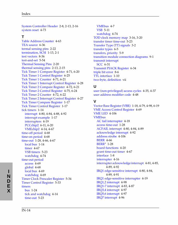
Index
INDEX
System Controller Header 2-8, 2-13, 2-16system reset 4-73
TTable Address Counter 4-63TEA source 6-36termal sensing pins 2-22termination, SCSI 1-13, 2-1test vectors 8-36test-and-set 5-54Thermal Sensing Pins 2-20thermal sensing pins 2-13, 2-15Tick Timer 1 Compare Register 4-71, 6-20Tick Timer 1 Control Register 6-25Tick Timer 1 Counter 4-71, 6-21Tick Timer 1 Interrupt Control Register 6-28Tick Timer 2 Compare Register 4-72, 6-21Tick Timer 2 Control Register 4-75, 6-24Tick Timer 2 Counter 4-72, 6-22Tick Timer 2 Interrupt Control Register 6-27Tick Timer Compare Register 1-17Tick Timer Control Register 1-17tick timers 1-14
interrupt 4-80, 4-84, 4-88, 4-92interrupt example 1-17interrupters 4-19PCCchip2 6-11, 6-20VMEchip2 4-14, 4-67
time-off period 4-68time-on period 4-68time-out 1-28, 4-66, 4-67
local bus 1-14timer 4-67VSB timers 5-23watchdog 4-74
time-out periodaccess 4-69global 4-68local bus 4-69watchdog 4-69
Timer Clock Prescaler Register 5-34Timer Control Register 5-33timers
bus 1-24tick and watchdog 4-14time-out 5-23
VMEbus 4-7VSB 5-11watchdog 4-74
TOD clock memory map 3-16, 3-20transfer timer time-out 5-23Transfer Type (TT) signals 3-2transfer types 6-5transfers, priority 5-9transition module connection diagrams 9-1transmit interrupt
SCC 6-31Transmit PIACK Register 6-34triple bit error 8-6TTL interface 1-10two-byte, definition vii
Uuser (non-privileged) access cycles 4-35, 4-37user address modifier code 4-48
VVector Base Register (VBR) 1-18, 4-79, 4-98, 6-19VME Access Control Register 4-69VME LED 4-106VMEbus
AC fail interrupter 4-18access time-out 1-28ACFAIL interrupt 4-80, 4-84, 4-89acknowledge interrupt 4-92address strobe 4-106BERR 4-66BERR* 1-28board functions 4-20grant time-out timer 4-67interface 1-8interrupter 4-16interrupter acknowledge interrupt 4-81, 4-85,
4-89, 4-92IRQ1 edge-sensitive interrupt 4-80, 4-84,
4-89, 4-91IRQ1 edge-sensitive interrupter 4-19IRQ1,2 interrupt 4-98IRQ1-7 interrupt 4-83, 4-87IRQ3,4 interrupt 4-97IRQ5,6 interrupt 4-97IRQ7 interrupt 4-96
IN-14
Index
INDEX
IRQ7-1 interrupters 4-20map decoder enable 4-47master 4-7, 4-11, 4-114master write post error interrupt 4-80, 4-84,
4-89release mode 4-58request level 4-56, 4-57requester 4-13slave 4-9slave map decoders 4-26specification vSYSFAIL interrupt 4-80, 4-84, 4-89timer 4-18to local bus interface 4-9
VMEbus Arbiter Time-out Control Register 4-67
VMEbus Global Time-out Control Register 4-68VMEbus Interrupter Control Register 4-63VMEbus Interrupter Vector Register 4-64VMEbus Slave
Address Modifier Select Register 1 4-36Address Modifier Select Register 2 4-34Address Translation Address Offset Register
1 4-30Address Translation Address Offset Register
2 4-32Address Translation Select Register 1 4-31Address Translation Select Register 2 4-32Ending Address Register 1 4-29Ending Address Register 2 4-29GCSR Board Address Register 4-46GCSR Group Address Register 4-46Starting Address Register 1 4-29Starting Address Register 2 4-30Write Post and Snoop Control Register 1 4-35Write Post and Snoop Control Register 2 4-33
VMEbus System Controller 4-17VMEchip2
BERR* 1-28block diagram 4-5DMA Controller 4-52features 4-1functional blocks 4-4GCSR programming model 4-107GCSR registers 4-109global control and status registers 4-20
introduction 4-1LCSR programming model 4-21LCSR registers 4-21local bus interrupter and interrupt
handler 4-18local bus to VMEbus DMA controller 4-11local bus to VMEbus interface 4-4memory map, LCSR Summary 4-22programming GCSR 4-109programming local bus interrupter 4-77programming local bus to VMEbus map
decoders 4-37programming tick and watchdog timers 4-67programming VMEbus slave map
decoders 4-26programming VMEchip2 DMA
controller 4-52tick and watchdog timers 4-14VMEboard functions 4-20VMEbus interrupter 4-16, 4-19VMEbus system controller 4-17VMEbus to local bus interface 4-9
VMEchip2 Board Status/Control Register 4-113
VMEchip2 ID Register 4-111VMEchip2 LM/SIG Register 4-111VMEchip2 Memory Map (GCSR
Summary) 4-110VMEchip2 Revision Register 4-111VSB
access time-out period 5-33access timer 5-11backplane 5-13, 5-24block transfer 5-8block transfers 5-12bus error 5-24dynamic bus sizing 5-11error 5-53global interrupt 5-59interface 1-8interrupt 5-28, 5-30interrupt acknowledge complete
interrupt 5-19, 5-28, 5-30interrupt acknowledge complete interrupt
flag 5-27interrupt arbitration ID 5-58
IN-15
Index
INDEX
interrupt flag 5-27interrupt handler 5-18, 5-57interrupt request 5-53interrupter 5-16LED control 5-23lock signal 5-63, 5-67master interface 5-11mastership 5-31memory map 3-2requester 5-14requester and serial arbiter 5-13software interrupt flag 5-60specification vto local bus interface 5-5transfer time-out period 5-34transfer timer 5-11write post error interrupt 5-28, 5-30write post interrupt 5-59write post interrupt flag 5-60
VSB Error Address Register 5-69VSB Error Status Register 5-56VSB Interrupt Control Register 5-57VSB Interrupt Enable Register 5-59VSB Interrupt Status Register 5-60VSB Interrupt Vector Register 5-58VSB interrupt-acknowledge cycles 5-57VSB Requester Control/Status Register 5-31VSB Slave 1
Address Offset Register 5-61Address Range Register 5-61Attribute Register 5-62
VSB Slave 2Address Offset Register 5-65Address Range Register 5-65Attribute Register 5-66
VSB slave interface 5-5VSBchip2
BCSRs 5-50BERR* 1-29block diagram 5-4description 5-3features 5-1ID 5-53introduction 5-1LCSRs 5-20local bus interrupter 5-18
local control/status registers 5-19version 5-53VSB interrupt handler 5-18VSB interrupter 5-16
WWatchdog Time-out Control Register 4-69watchdog time-out period 4-69watchdog timer 1-14, 4-14, 4-15, 4-67Watchdog Timer Control Register 4-74WDTO bits 4-15word, definition viiwrite cycles 5-37, 5-40, 5-43, 5-46, 5-62, 5-66write post 4-35, 4-43, 4-44, 4-45, 4-48, 4-49
buffer 4-7, 4-9, 5-6, 5-10bus error interrupter 4-19enable 5-37, 5-40, 5-43, 5-46, 5-63, 5-67enable/disable 4-33error 5-47, 5-60, 5-69error address 5-26error interrupt 5-19, 5-33timer 4-8VSB cycle 5-59
write posting 4-7, 4-10, 4-39definition 4-7
write wrong parity 7-12write-per-bit 7-8writes, random and burst 8-2
Zzero fill capability, MCECC 8-36zero fill memory 8-22
IN-16