Embed Size (px)
Citation preview
Ning Cao, Staff Engineer, Nano-Fabrication Lab, UCSB
SiNx Etch Recipe using RIE#3
Sample: PR-ridge-pattern on 1.2 m-thick SiNx/Si substrate.
Results:
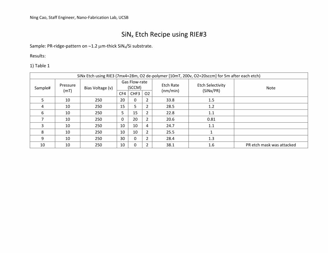
1) Table 1
SiNx Etch using RIE3 (7mx4=28m, O2 de-polymer [10mT, 200v, O2=20sccm] for 5m after each etch)
Sample# Pressure
(mT) Bias Voltage (v)
Gas Flow-rate (SCCM)
Etch Rate (nm/min)
Etch Selectivity (SiNx/PR)
Note CF4 CHF3 O2
5 10 250 20 0 2 33.8 1.5
4 10 250 15 5 2 28.5 1.2
6 10 250 5 15 2 22.8 1.1
7 10 250 0 20 2 20.6 0.81
3 10 250 10 10 4 24.7 1.1
8 10 250 10 10 2 25.5 1
9 10 250 30 0 2 28.4 1.3
10 10 250 10 0 2 38.1 1.6 PR etch mask was attacked
Ning Cao, Staff Engineer, Nano-Fabrication Lab, UCSB
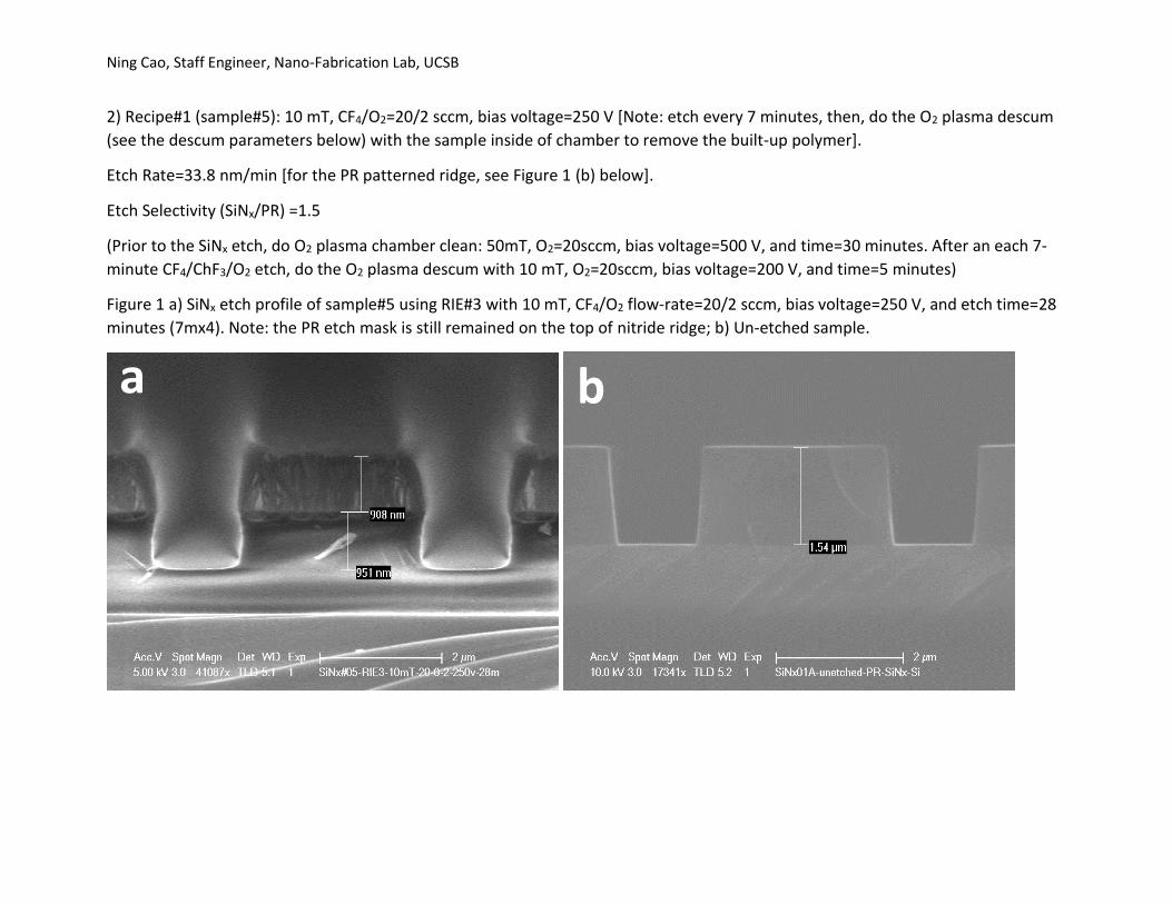
2) Recipe#1 (sample#5): 10 mT, CF4/O2=20/2 sccm, bias voltage=250 V [Note: etch every 7 minutes, then, do the O2 plasma descum
(see the descum parameters below) with the sample inside of chamber to remove the built-up polymer].
Etch Rate=33.8 nm/min [for the PR patterned ridge, see Figure 1 (b) below].
Etch Selectivity (SiNx/PR) =1.5
(Prior to the SiNx etch, do O2 plasma chamber clean: 50mT, O2=20sccm, bias voltage=500 V, and time=30 minutes. After an each 7-
minute CF4/ChF3/O2 etch, do the O2 plasma descum with 10 mT, O2=20sccm, bias voltage=200 V, and time=5 minutes)
Figure 1 a) SiNx etch profile of sample#5 using RIE#3 with 10 mT, CF4/O2 flow-rate=20/2 sccm, bias voltage=250 V, and etch time=28
minutes (7mx4). Note: the PR etch mask is still remained on the top of nitride ridge; b) Un-etched sample.
a b
Ning Cao, Staff Engineer, Nano-Fabrication Lab, UCSB
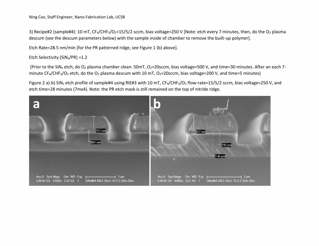
3) Recipe#2 (sample#4): 10 mT, CF4/CHF3/O2=15/5/2 sccm, bias voltage=250 V [Note: etch every 7 minutes, then, do the O2 plasma
descum (see the descum parameters below) with the sample inside of chamber to remove the built-up polymer].
Etch Rate=28.5 nm/min [for the PR patterned ridge, see Figure 1 (b) above].
Etch Selectivity (SiNx/PR) =1.2
(Prior to the SiNx etch, do O2 plasma chamber clean: 50mT, O2=20sccm, bias voltage=500 V, and time=30 minutes. After an each 7-
minute CF4/CHF3/O2 etch, do the O2 plasma descum with 10 mT, O2=20sccm, bias voltage=200 V, and time=5 minutes)
Figure 2 a)-b) SiNx etch profile of sample#4 using RIE#3 with 10 mT, CF4/CHF3/O2 flow-rate=15/5/2 sccm, bias voltage=250 V, and
etch time=28 minutes (7mx4). Note: the PR etch mask is still remained on the top of nitride ridge.
a b
Ning Cao, Staff Engineer, Nano-Fabrication Lab, UCSB
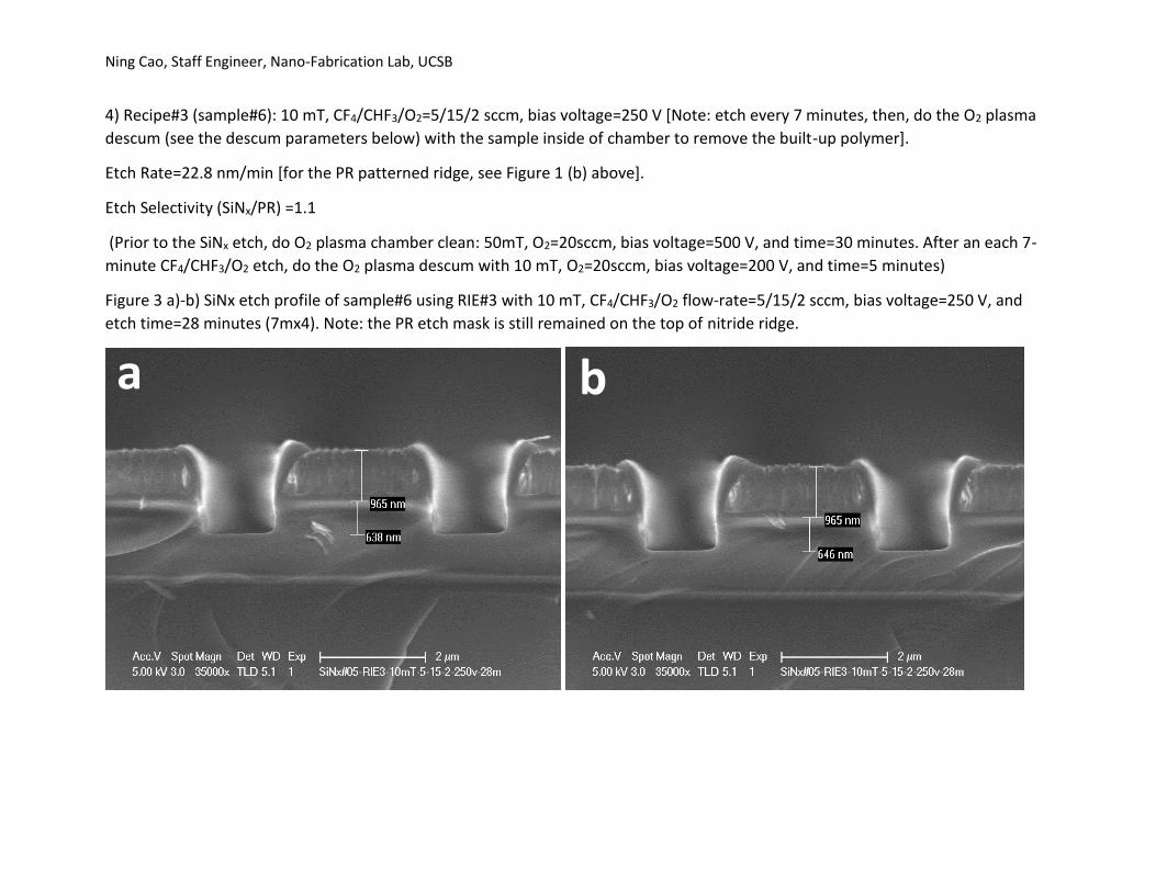
4) Recipe#3 (sample#6): 10 mT, CF4/CHF3/O2=5/15/2 sccm, bias voltage=250 V [Note: etch every 7 minutes, then, do the O2 plasma
descum (see the descum parameters below) with the sample inside of chamber to remove the built-up polymer].
Etch Rate=22.8 nm/min [for the PR patterned ridge, see Figure 1 (b) above].
Etch Selectivity (SiNx/PR) =1.1
(Prior to the SiNx etch, do O2 plasma chamber clean: 50mT, O2=20sccm, bias voltage=500 V, and time=30 minutes. After an each 7-
minute CF4/CHF3/O2 etch, do the O2 plasma descum with 10 mT, O2=20sccm, bias voltage=200 V, and time=5 minutes)
Figure 3 a)-b) SiNx etch profile of sample#6 using RIE#3 with 10 mT, CF4/CHF3/O2 flow-rate=5/15/2 sccm, bias voltage=250 V, and
etch time=28 minutes (7mx4). Note: the PR etch mask is still remained on the top of nitride ridge.
a b
Ning Cao, Staff Engineer, Nano-Fabrication Lab, UCSB
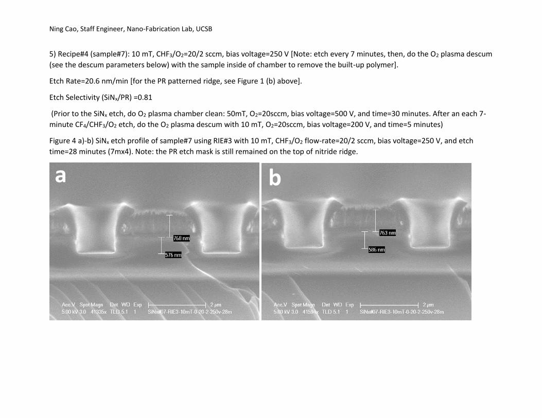
5) Recipe#4 (sample#7): 10 mT, CHF3/O2=20/2 sccm, bias voltage=250 V [Note: etch every 7 minutes, then, do the O2 plasma descum
(see the descum parameters below) with the sample inside of chamber to remove the built-up polymer].
Etch Rate=20.6 nm/min [for the PR patterned ridge, see Figure 1 (b) above].
Etch Selectivity (SiNx/PR) =0.81
(Prior to the SiNx etch, do O2 plasma chamber clean: 50mT, O2=20sccm, bias voltage=500 V, and time=30 minutes. After an each 7-
minute CF4/CHF3/O2 etch, do the O2 plasma descum with 10 mT, O2=20sccm, bias voltage=200 V, and time=5 minutes)
Figure 4 a)-b) SiNx etch profile of sample#7 using RIE#3 with 10 mT, CHF3/O2 flow-rate=20/2 sccm, bias voltage=250 V, and etch
time=28 minutes (7mx4). Note: the PR etch mask is still remained on the top of nitride ridge.
a b
Ning Cao, Staff Engineer, Nano-Fabrication Lab, UCSB
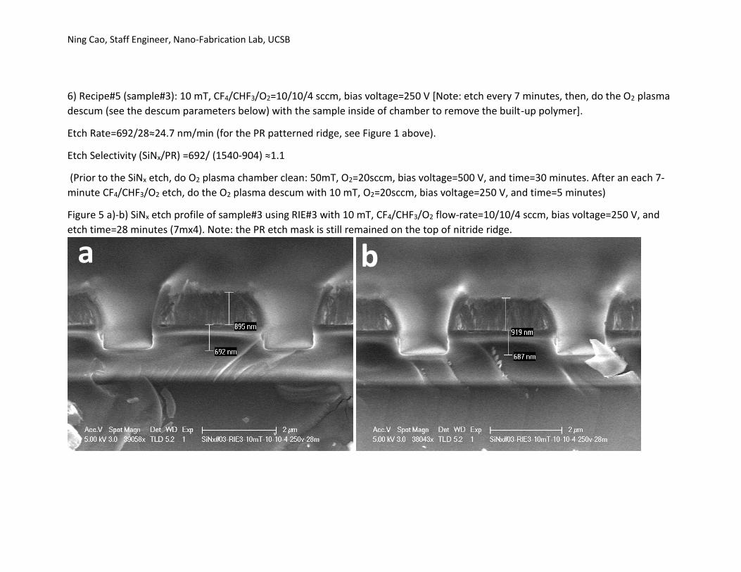
6) Recipe#5 (sample#3): 10 mT, CF4/CHF3/O2=10/10/4 sccm, bias voltage=250 V [Note: etch every 7 minutes, then, do the O2 plasma
descum (see the descum parameters below) with the sample inside of chamber to remove the built-up polymer].
Etch Rate=692/28≈24.7 nm/min (for the PR patterned ridge, see Figure 1 above).
Etch Selectivity (SiNx/PR) =692/ (1540-904) ≈1.1
(Prior to the SiNx etch, do O2 plasma chamber clean: 50mT, O2=20sccm, bias voltage=500 V, and time=30 minutes. After an each 7-
minute CF4/CHF3/O2 etch, do the O2 plasma descum with 10 mT, O2=20sccm, bias voltage=250 V, and time=5 minutes)
Figure 5 a)-b) SiNx etch profile of sample#3 using RIE#3 with 10 mT, CF4/CHF3/O2 flow-rate=10/10/4 sccm, bias voltage=250 V, and
etch time=28 minutes (7mx4). Note: the PR etch mask is still remained on the top of nitride ridge.
a b
Ning Cao, Staff Engineer, Nano-Fabrication Lab, UCSB
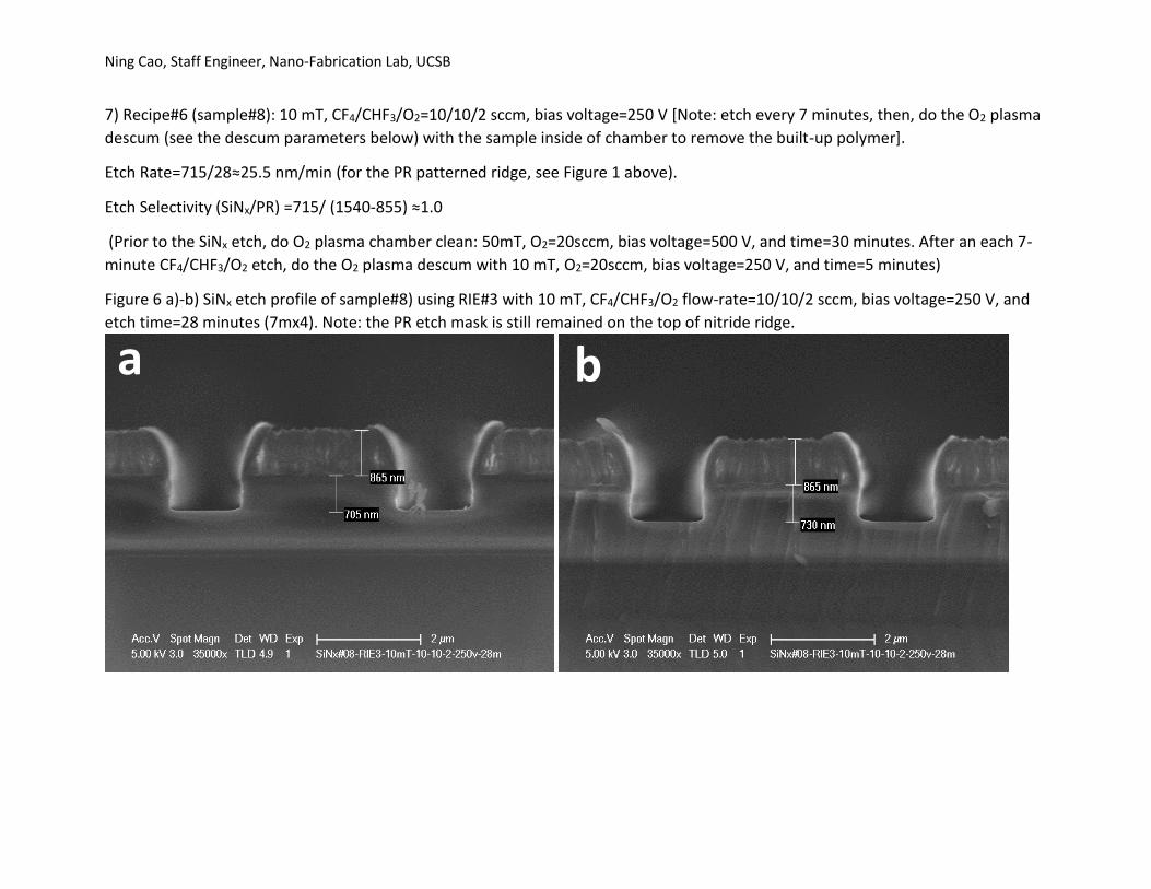
7) Recipe#6 (sample#8): 10 mT, CF4/CHF3/O2=10/10/2 sccm, bias voltage=250 V [Note: etch every 7 minutes, then, do the O2 plasma
descum (see the descum parameters below) with the sample inside of chamber to remove the built-up polymer].
Etch Rate=715/28≈25.5 nm/min (for the PR patterned ridge, see Figure 1 above).
Etch Selectivity (SiNx/PR) =715/ (1540-855) ≈1.0
(Prior to the SiNx etch, do O2 plasma chamber clean: 50mT, O2=20sccm, bias voltage=500 V, and time=30 minutes. After an each 7-
minute CF4/CHF3/O2 etch, do the O2 plasma descum with 10 mT, O2=20sccm, bias voltage=250 V, and time=5 minutes)
Figure 6 a)-b) SiNx etch profile of sample#8) using RIE#3 with 10 mT, CF4/CHF3/O2 flow-rate=10/10/2 sccm, bias voltage=250 V, and
etch time=28 minutes (7mx4). Note: the PR etch mask is still remained on the top of nitride ridge.
a b
Ning Cao, Staff Engineer, Nano-Fabrication Lab, UCSB
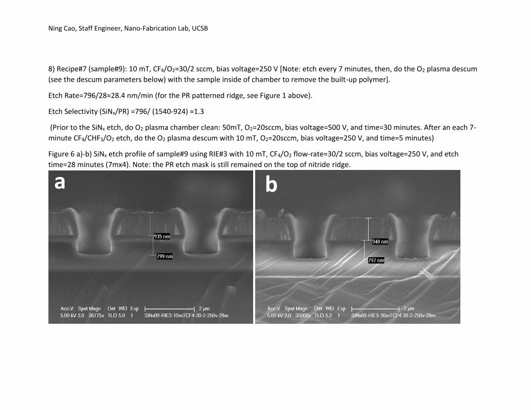
8) Recipe#7 (sample#9): 10 mT, CF4/O2=30/2 sccm, bias voltage=250 V [Note: etch every 7 minutes, then, do the O2 plasma descum
(see the descum parameters below) with the sample inside of chamber to remove the built-up polymer].
Etch Rate=796/28≈28.4 nm/min (for the PR patterned ridge, see Figure 1 above).
Etch Selectivity (SiNx/PR) =796/ (1540-924) ≈1.3
(Prior to the SiNx etch, do O2 plasma chamber clean: 50mT, O2=20sccm, bias voltage=500 V, and time=30 minutes. After an each 7-
minute CF4/CHF3/O2 etch, do the O2 plasma descum with 10 mT, O2=20sccm, bias voltage=250 V, and time=5 minutes)
Figure 6 a)-b) SiNx etch profile of sample#9 using RIE#3 with 10 mT, CF4/O2 flow-rate=30/2 sccm, bias voltage=250 V, and etch
time=28 minutes (7mx4). Note: the PR etch mask is still remained on the top of nitride ridge.
a b
Ning Cao, Staff Engineer, Nano-Fabrication Lab, UCSB
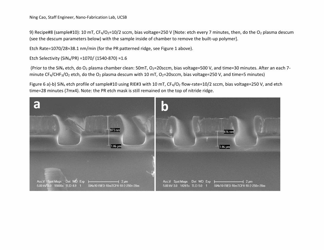
9) Recipe#8 (sample#10): 10 mT, CF4/O2=10/2 sccm, bias voltage=250 V [Note: etch every 7 minutes, then, do the O2 plasma descum
(see the descum parameters below) with the sample inside of chamber to remove the built-up polymer].
Etch Rate=1070/28≈38.1 nm/min (for the PR patterned ridge, see Figure 1 above).
Etch Selectivity (SiNx/PR) =1070/ (1540-870) ≈1.6
(Prior to the SiNx etch, do O2 plasma chamber clean: 50mT, O2=20sccm, bias voltage=500 V, and time=30 minutes. After an each 7-
minute CF4/CHF3/O2 etch, do the O2 plasma descum with 10 mT, O2=20sccm, bias voltage=250 V, and time=5 minutes)
Figure 6 a)-b) SiNx etch profile of sample#10 using RIE#3 with 10 mT, CF4/O2 flow-rate=10/2 sccm, bias voltage=250 V, and etch
time=28 minutes (7mx4). Note: the PR etch mask is still remained on the top of nitride ridge.
a b