Embed Size (px)
Citation preview
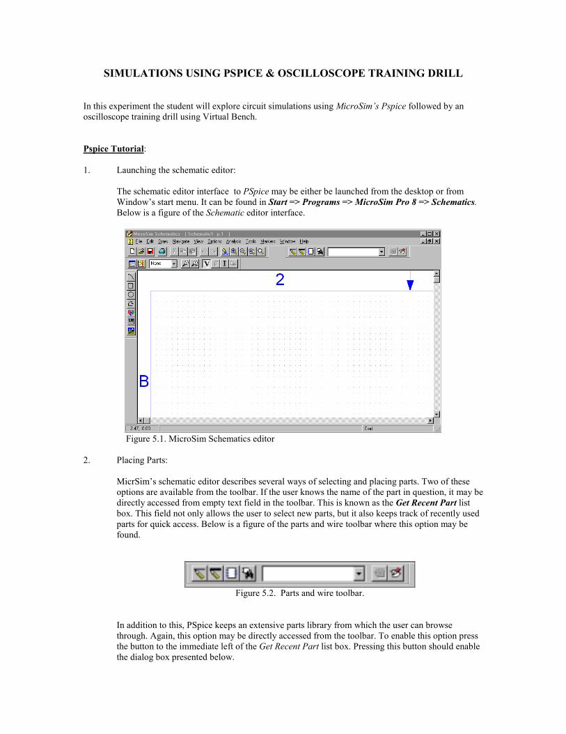
SIMULATIONS USING PSPICE & OSCILLOSCOPE TRAINING DRILL
In this experiment the student will explore circuit simulations using MicroSim’s Pspice followed by an
oscilloscope training drill using Virtual Bench.
Pspice Tutorial:
1. Launching the schematic editor:
The schematic editor interface to PSpice may be either be launched from the desktop or from
Window’s start menu. It can be found in Start => Programs => MicroSim Pro 8 => Schematics.
Below is a figure of the Schematic editor interface.
Figure 5.1. MicroSim Schematics editor
2. Placing Parts:
MicrSim’s schematic editor describes several ways of selecting and placing parts. Two of these
options are available from the toolbar. If the user knows the name of the part in question, it may be
directly accessed from empty text field in the toolbar. This is known as the Get Recent Part list
box. This field not only allows the user to select new parts, but it also keeps track of recently used
parts for quick access. Below is a figure of the parts and wire toolbar where this option may be
found.
Figure 5.2. Parts and wire toolbar.
In addition to this, PSpice keeps an extensive parts library from which the user can browse
through. Again, this option may be directly accessed from the toolbar. To enable this option press
the button to the immediate left of the Get Recent Part list box. Pressing this button should enable
the dialog box presented below.

Figure5. 3. Part Browser dialog box.
Figure 5.3 above presents one of the two dialog boxes that may appear. These may be the Part
Browser Advanced and Part Browser Basic dialog boxes. Although both modes can be used to
select parts, Part Browser Advanced provides extended options for part placement. These include
descriptive searches as well as a symbolic representation of the selected part. You can switCH-
Between modes by selecting the Basic or Advanced buttons. In addition to the above method the
part browser dialog box may also be accessed at Draw => Get New Part or by using the
<Ctrl-G>shortcut.
3. Placing Wires:
PSpice defines several methods for wire placement. Again, this option may be accessed from the
toolbar in Figure 5.2. To place wires simply select the leftmost available icon on the toolbar. In
addition to this method wires may be placed from both Draw => Wire or by selecting the
<Ctrl-W>shortcut.
4. Placing Markers:
Markers allow users to specify where voltage and current waveforms are to be analyzed and
simulated on the circuit from the schematic. Markers may be accessed by selecting Markers from
the drop down menu. Below is a description of several of the available options.
Mark Voltage Level - Measures voltage level with respect to ground.
Mark Voltage Differential - Measures the differential voltage between two user defined
points.
Mark Current into Pin - Measures the current entering a node.
Mark Advanced - Provides several advanced measuring options including
decibel readings of voltage and current.
4. Setting up a Simulation:

PSpice requires that all schematics be saved before any simulations may be conducted. Once a
schematic has been saved, the user should access Analysis => Setup from the drop down menu.
This should bring up the following dialog box.
Figure 5.4. Setup dialog box
Figure 5.4 presents the numerous available simulation options. In this case, we will only be
concerned with selecting Bias Point Detail as well as Transient options. These options will allow
the user to plot time varying signals. Enable these options by placing a checkmark next to each.
In addition to selecting Transient from the dialog box, click on the Transient button. You should
see the following dialog box appear.
Figure 5.5 Transient dialog box
The Transient dialog box allows users to set final simulation times as well integer step values for
simulation. Smaller step values allow for increased resolution in resulting plots, however, this comes at the
expense of increased simulation time. Care must be taken at both extremes. Large step values can results in
coarse output plots or even worse the resulting signal may become aliased. To prevent aliasing make sure
your print step is smaller than half the period of the highest frequency signal in your circuit.
Once a step size and a final time have been selected you are now able to proceed with the simulation. Exit
the Transient dialog box by clicking on the OK button. Then proceed to exit the Analysis Setup by clicking
on the Close button. To initiate a simulation go to Analysis => Simulate. Doing so should begin the
simulation as long as there are no errors in your circuit. At this point you should see a dialog box that
resembles Figure 5.6 on your screen.

Figure 5.6 Simulation dialog box
Once this portion of the simulation has finished, results are usually displayed graphically through the use of
the Probe interface in Pspice. Figure 5.7 presents an example Probe display. In the case where your
simulation has finished running and you do not see the Probe display go to Analysis => Run Probe. This
should work provided your circuit is error free.
Note: Remember to place markers before you run your simulations.
Figure 5.7 Sample Probe display
5. Useful Shortcuts:

Below is a list of frequently used shortcuts. These options can be additionally accessed from the
available toolbars in the schematic editor.
<Ctrl-F> Provides a mirror image of the part by flipping
it completely over
<Ctrl-G> Displays the Get New Part dialog box
<Ctrl-P> Selects Get Recent Part list box
<Ctrl-R> Rotates selected part in increments of 90o.
<Ctrl-T> Creates a text box
<Ctrl-W> Places wire
6. Basic Parts List:
Pspice provides an extensive parts list. Its libraries may contain thousands of components. In order
to simplify your searCH-Below is a list of basic parts that you may need for the course of the
semester.
R Resistor
C Capacitor
L Inductor
egnd Earth Ground
Vdc DC Voltage Source
Vsin Sinusoidal Voltage Source
Vpulse Square Wave Voltage Source
uA741 741 Op-amp
Exercise:
At this point you are now ready to begin simulating some simple circuits. We will begin by simulating
some of the same circuits you have built in the previous labs.
1. Simulate the circuits in Figures 5.8 (a), (b), and (c). Make sure to measure all branch voltages and
currents. Plot results. Compare these with the results obtained in the previous labs. Are there any
significant differences in results? If so, explain.
Note: Provide separate plots for voltage and current. Make sure to label your plots.
5.8 (a) 5.8 (b)

5.8(c)
2. Simulate the circuit in Figure 5.9. Notice that the input source is no longer DC. Instead we will use
an alternating source (AC) voltage. Display both input and output voltages plots on the same
graph. Do this for both a sinusoidal input (Vsin) source as well as for a square wave (Vpulse)
source. Below are the parameters you need to set the sources to. You may change a source's or
any parts par parameters by double clicking on the part.
Vsin: Vpulse:
DC = 0 DC = 0
AC = 5 AC = 5
Voff = 0 V1 = 5
Vamp = 5 V2 = -5
Freq = 1000 TD = 0
TD = 0 TR = 0.00001m
DF = 0 TF = 0.00001m
Phase = 0 PW = 0.5m
PER = 1m
Note: Do not skip spaces.
Figure 5.9
3. Dependent Sources in PSpice

There are four different types of dependent sources all which can be found and utilized in PSpice. Table 1-
1 shows the different types of dependent sources as well as the part name that PSpice uses to identify them
and Figure 5.10 illustrates each sources symbol.
Sources Part Name
Voltage controlled voltage source (VCVS) E
Voltage controlled current source (VCVS) G
Current controlled voltage source (CCVS) H
Current controlled current source (CCCS) F
Table 1-1
Figure 5.10
As is shown in Figure 5.10, each dependent source has two sources associated with the part. The source
(either voltage or current) on the left hand side of the part is the source that requires the dependence. The
source on the right hand side of the part (the source with the circle) is the source that is doing the
controlling based on a voltage or a current from some other element in the circuit. A clearer explanation
can be seen with an example.
Example: Simulate the circuit in Figure 5.11
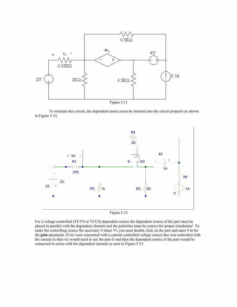
Figure 5.11
To simulate this circuit, the dependent source must be inserted into the circuit properly as shown
in Figure 5.12.
Figure 5.12
For a voltage controlled (VCVS or VCCS) dependent source the dependent source of the part must be
placed in parallel with the dependent element and the polarities must be correct for proper simulation! To
make the controlling source the necessary 4 times Vx you must double click on the part and enter 4 in for
the gain parameter. If we were concerned with a current controlled voltage source that was controlled with
the current Ix then we would need to use the part G and then the dependent source of the part would be
connected in series with the dependent element as seen in Figure 5.13.
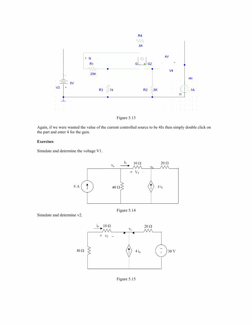
Figure 5.13
Again, if we were wanted the value of the current controlled source to be 4Ix then simply double click on
the part and enter 4 for the gain.
Exercises
Simulate and determine the voltage V1.
Figure 5.14
Simulate and determine v2.
Figure 5.15
Tutorial B
Oscilloscope Training Drill
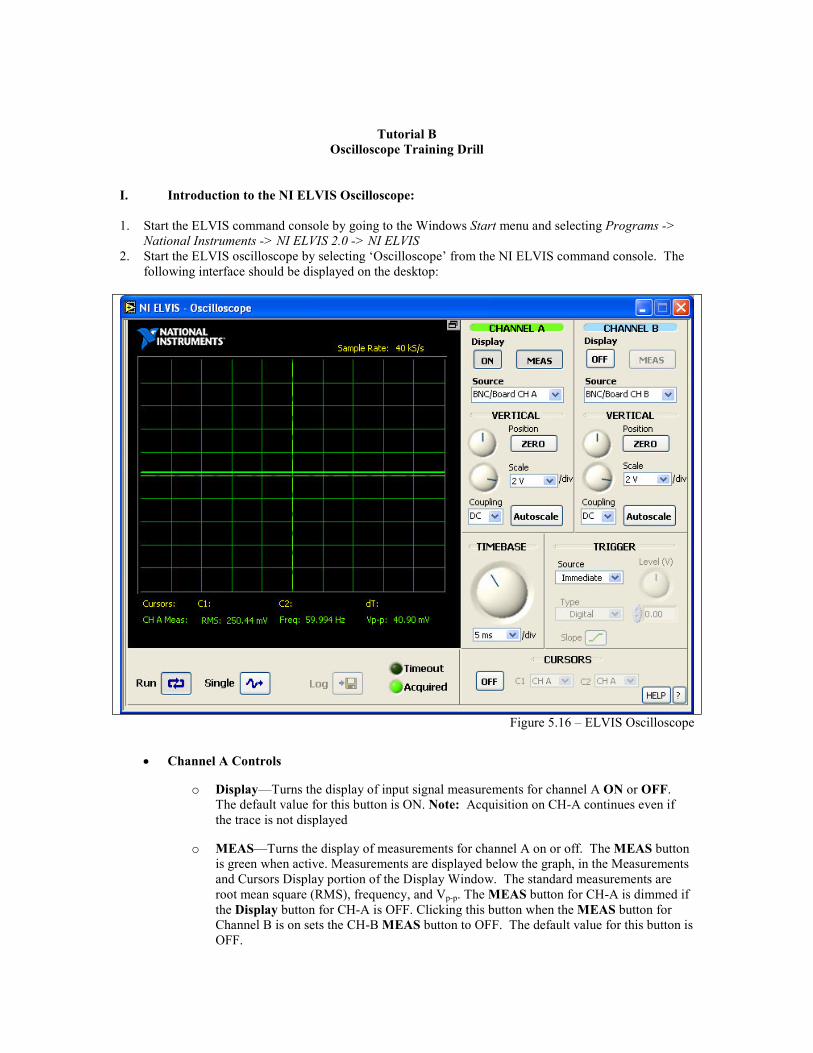
I. Introduction to the NI ELVIS Oscilloscope:
1. Start the ELVIS command console by going to the Windows Start menu and selecting Programs ->
National Instruments -> NI ELVIS 2.0 -> NI ELVIS
2. Start the ELVIS oscilloscope by selecting ‘Oscilloscope’ from the NI ELVIS command console. The
following interface should be displayed on the desktop:
Figure 5.16 – ELVIS Oscilloscope
• Channel A Controls
o Display—Turns the display of input signal measurements for channel A ON or OFF.
The default value for this button is ON. Note: Acquisition on CH-A continues even if
the trace is not displayed
o MEAS—Turns the display of measurements for channel A on or off. The MEAS button
is green when active. Measurements are displayed below the graph, in the Measurements
and Cursors Display portion of the Display Window. The standard measurements are
root mean square (RMS), frequency, and Vp-p. The MEAS button for CH-A is dimmed if
the Display button for CH-A is OFF. Clicking this button when the MEAS button for
Channel B is on sets the CH-B MEAS button to OFF. The default value for this button is
OFF.

o Source—Selects the signal source for the measurement on CH-A. You can select
ACH<0..2>, ACH5, the BNC/Board CH-A, the function generator FUNC_OUT signal,
the function generator SYNC_OUT signal, and the DMM VOLTAGE channel (routed
to ACH7). The default value for this control is BNC/Board CH-A.
o Vertical Position Knob—Adjusts the vertical position of the CH-A trace by applying a
positive or negative vertical offset. The default is zero offset. The offset is referenced
from the zero point of the graph. This offset value is not applied to the actual acquired
data.
o Zero—Centers CH-A on the vertical zero point of the graph. This action does not affect
the actual acquired data. The default is no action.
o Scale/Div—Selects the vertical sensitivity for the channel A trace. Sensitivity is defined
as the amount of voltage represented by each horizontal line on the graph. The units are
in volts/division. The Scale/Div options are 10mV, 20mV, 50mV, 100mV, 200mV,
500mV, 1V, 2V, and 5V. The default value for this control is 2V.
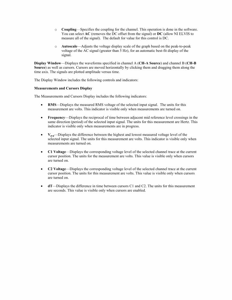
o Coupling—Specifies the coupling for the channel. This operation is done in the
software. You can select AC (removes the DC offset from the signal) or DC (allow NI
ELVIS to measure all of the signal). The default for value for this control is DC.
o Autoscale—Adjusts the voltage display scale of the graph based on the peak-to-peak
voltage of the AC signal (greater than 5 Hz), for an automatic best-fit display of the
signal.
• Channel B Controls
o Display—Turns the display of the CH-B trace on or off. The default value for this button
is ON. Note Acquisition on CH-B continues even if the trace is not displayed
o MEAS—Turns the display of measurements for channel B on or off. The MEAS button
is green when active. Measurements are displayed below the graph, in the Measurements
and Control Display portion of the Display Window. The standard measurements are
RMS, frequency, and Vp-p. The MEAS button for CH-B is dimmed if the Display button
for CH-B is OFF. Turning this feature on when the CH-A MEAS button is on, sets the
CH-A MEAS button to off. The default value for this button is OFF.
o Source—Selects the signal source for the measurement on CH-B. You can select
ACH<0..2>, ACH5, the BNC/Board CH-B, the function generator FUNC_OUT signal,
the function generator SYNC_OUT signal, and the DMM VOLTAGE channel (routed
to ACH7). The default value for this control is BNC/Board CH-B.
o Vertical Position Knob—Adjusts the vertical position of the channel B trace by
applying a positive or negative vertical offset. The offset is referenced from the zero
point of the graph. This offset value is not applied the actual acquired data. The default is
zero offset.
o Zero—Centers the CH-B trace on the vertical zero point of the graph. The default is no
action. This action does not affect the actual acquired data.
o Scale/Div—Selects the vertical sensitivity for the channel B trace. The units are in
volts/division. Sensitivity is defined as the amount of voltage represented by each
horizontal line on the graph. The Scale/Div options are 10 mV, 20 mV, 50 mV, 100 mV,
200 mV, 500 mV, 1 V, 2 V, and 5 V. The default value for this control is 2 V.
o Coupling—Specifies the coupling for the channel. This operation is done in the software.
You can select AC (removes the DC offset from the signal) or DC (allow NI ELVIS to
measure all of the signal). The default for value for this control is DC.
o Autoscale—Adjusts the voltage display scale of the graph based on the peak-to-peak
voltage of the AC signal (greater than 5 Hz), for an automatic best-fit display of the
signal.
Display Window—Displays the waveforms specified in channel A (CH-A Source) and channel B (CH-B
Source) as well as cursors. Cursors are moved horizontally by clicking them and dragging them along the
time axis. The signals are plotted amplitude versus time.
The Display Window includes the following controls and indicators:
Measurements and Cursors Display
The Measurements and Cursors Display includes the following indicators:
• RMS—Displays the measured RMS voltage of the selected input signal. The units for this
measurement are volts. This indicator is visible only when measurements are turned on.
• Frequency—Displays the reciprocal of time between adjacent mid reference level crossings in the
same direction (period) of the selected input signal. The units for this measurement are Hertz. This
indicator is visible only when measurements are in progress.
• Vp-p—Displays the difference between the highest and lowest measured voltage level of the
selected input signal. The units for this measurement are volts. This indicator is visible only when
measurements are turned on.
• C1 Voltage—Displays the corresponding voltage level of the selected channel trace at the current
cursor position. The units for the measurement are volts. This value is visible only when cursors
are turned on.
• C2 Voltage—Displays the corresponding voltage level of the selected channel trace at the current
cursor position. The units for this measurement are volts. This value is visible only when cursors
are turned on.
• dT—Displays the difference in time between cursors C1 and C2. The units for this measurement
are seconds. This value is visible only when cursors are enabled.

II. Introduction to the ELVIS Function Generator
1. Start the ELVIS function generator by selecting ‘Function Generator’ from the NI ELVIS
command console. The following interface should be displayed on the desktop:
Figure 5.17 – ELVIS Function Generator
The NI ELVIS - FGEN SFP is a top-level, stand-alone instrument that controls the function generator in the
NI ELVIS Benchtop Workstation. It allows setting of the following features:
• Waveform (sine, triangle, square)
• Tuning mode (basic low resolution - fast 8-bit fine frequency, ultrafine - slower 12-bit fine
frequency)
• Modulation (disabled, software—AM or FM using DAC0 or DAC1)
• Frequency adjust
• Amplitude (8-bit)
• DC offset (8-bit)
• Measure frequency of generated signal

You can control the function generator either through the NI ELVIS - FGEN SFP (Software mode) or the
hardware controls on the benchtop workstation (Manual mode). This section describes the software
controls. Refer to the NI ELVIS Benchtop Workstation section of Chapter 3, Hardware Overview, of the NI
ELVIS User Manual for more information on the hardware controls for the function generator.
The tab labeled “Large Amplitude Waveform” is capable of providing signals with amplitudes larger than
2.5Vpeak. The output from this panel is available on DAC0 NOT FUNC_OUT. The two signals CAN NOT
be active simultaneously, you must choose one output or the other. Also, please note that some of the built-
in functions WILL NOT WORK if DAC0 is used as the input.
III. Exercise 1:
1. Set the Oscilloscope Controls to the following:
• DC Coupling
• 0V Offset
• Trigger Immediate
2. Complete the following steps to measure a signal with the NI ELVIS - Scope SFP:
i. Connect the signal(s) you want to measure and the trigger signal, if desired, to the BNC
connector(s) on the front of the NI ELVIS Benchtop Workstation or to the corresponding inputs
on the NI ELVIS Prototyping Board.
ii. Launch the NI ELVIS - Scope SFP from the NI ELVIS Instrument Launcher. Refer to Launching
the SFP Instruments for more information.
iii. The NI ELVIS - Scope SFP starts running when launched. You should see the signal in the
Display Window.
iv. If needed, adjust the Trigger Source control to stabilize the signal in the Display Window. If you
have an external signal connected as the trigger signal, select SCOPE Trigger. If you want to use
one of the input channels as the trigger, select CHANNEL A or CHANNEL B from the Source
control.
v. Adjust the Timebase, Vertical Position, Scale, and other controls as desired.
You should now be able to read data on both channels CHA and CHB of the workbench.
3. Now configure the ELVIS Function Generator to the following settings:
i. Connect the Function Generator FUNC_OUT pin to the location where the signal is needed.
ii. Launch the NI ELVIS - FGEN SFP from the NI ELVIS Instrument Launcher.
iii. Choose the desired value from the Waveform, Peak Amplitude, DC Offset, Fine Frequency, and
Coarse Frequency controls.
iv. Click the On button on the NI ELVIS - FGEN SFP to begin generation.
4. Set the function generator to:
Frequency: 500 Hz
Duty Cycle: 50 %
Offset: 0 %
Amplitude: 5 Vpk
Input Signal Sine wave
5. Set both the function generator as well as the oscilloscope for continuos signal generation and
acquisition by pressing the Run or On buttons on either device.

You should now see a sine wave at a frequency of 500 Hz, 0 V offset, and 5Vpk. If you do not,
try pressing Autoscale on the front panel of the scope. Additionally, notice the parameters that
appear below the display. You should find helpful information on frequency, period, voltage
levels, offset, etc. More options may be configured in the General Settings tab.
6. On the front panel of the VB Scope try turning the knobs labeled Time Base, Volts/div, and V.
Position. Answer the following questions
Can you observe any differences in the displayed signal? If so, what do you observe? Do these
settings have any effect on the parameters displayed below the plot?
Now, press the button labeled Slope. What effect does this have on the display?
7. Select the option labeled Cursor on the front panel of the VB Scope display and set to the following:
CH-A
CH-B
You should now be able to drag cursors on the waveform observed on channel A of the display.
Note that you must enable channel B before selecting the cursor for channel B. Below the plot
you should observe information on the positions of the two cursors. This information should
include both voltage levels as well as differential times between the two cursors.
8. De-select the Cursor option on the scope. Now return to the FG display and switch through the
various different waveforms available on the display. You should be able to select between sine,
square, and triangular. Additional waveforms may also be user defined.
9. Set the output waveform of the FG to a square and then triangular wave. On the front panel of the FG
try turning the knob labeled Offset. Observe and answer the following questions.
Can you observe any differences in the displayed signal? If so, what do you observe? Do these
settings have any effect on the parameters displayed below the plot? Explain.
10. Set the displayed waveform to the same settings described in step (4), but now configure the channel
settings to AC coupling. Do you observe any changes in the displayed waveform?
Now, increase or decrease the DC offset of the signal. Is there any difference in the displayed
waveform? Should there be? Explain.
11. Set the oscilloscope to two different waveforms provided for by the instructor. These waveforms
should be at different offsets, amplitudes, frequencies, as well as duty cycles.
Note: Adding a DC offset to your waveform is NOT the same as moving the reference point on
the display. This should be apparent for the options displayed below the plots.
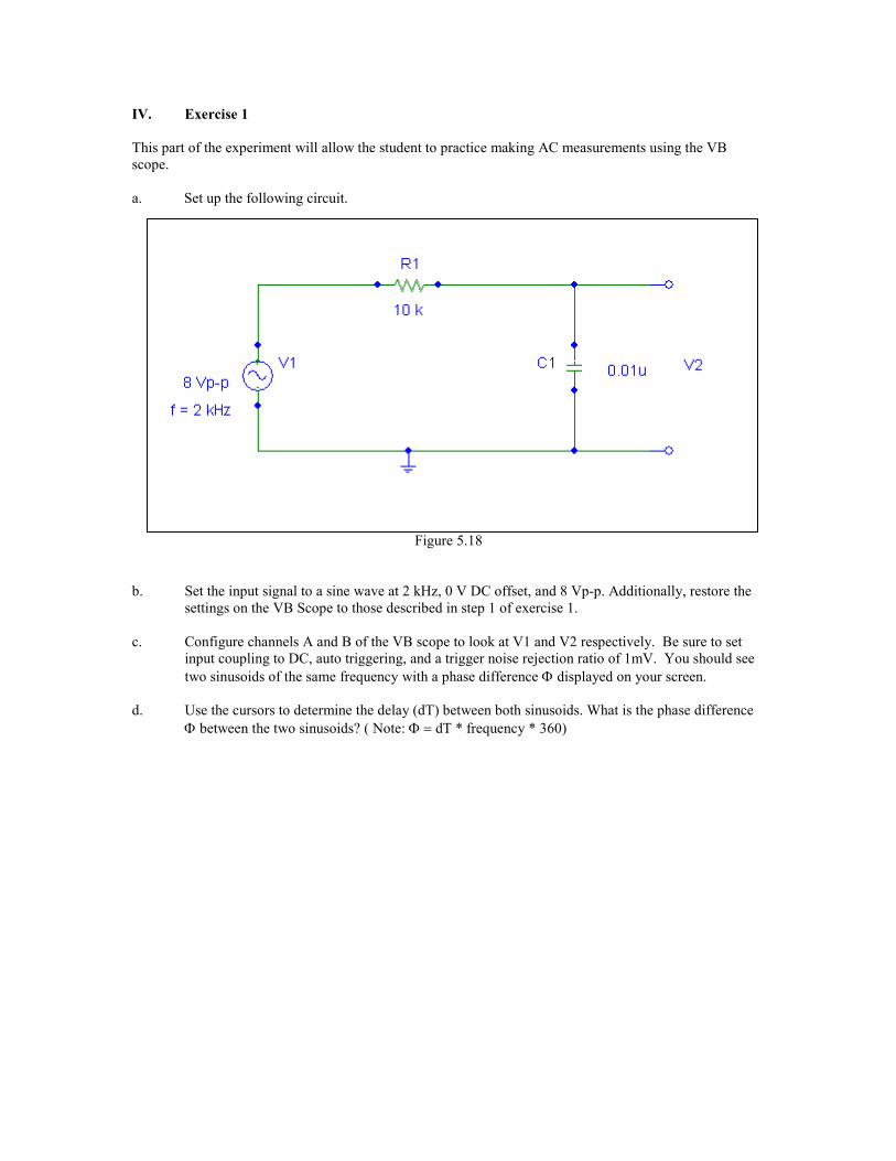
IV. Exercise 1
This part of the experiment will allow the student to practice making AC measurements using the VB
scope.
a. Set up the following circuit.
Figure 5.18
b. Set the input signal to a sine wave at 2 kHz, 0 V DC offset, and 8 Vp-p. Additionally, restore the
settings on the VB Scope to those described in step 1 of exercise 1.
c. Configure channels A and B of the VB scope to look at V1 and V2 respectively. Be sure to set
input coupling to DC, auto triggering, and a trigger noise rejection ratio of 1mV. You should see
two sinusoids of the same frequency with a phase difference Φ displayed on your screen.
d. Use the cursors to determine the delay (dT) between both sinusoids. What is the phase difference
Φ between the two sinusoids? ( Note: Φ = dT * frequency * 360)