Embed Size (px)
Citation preview

ECE 562 Cuk Converter (NL5 Simulation) Laboratory Page 1
SIMULATION WITH THE CUK TOPOLOGY ECE562: Power Electronics I
COLORADO STATE UNIVERSITY
Modified in Fall 2011

ECE 562 Cuk Converter (NL5 Simulation) Laboratory Page 2
PURPOSE: The purpose of this lab is to simulate the Cuk converter using NL5
to
better familiarize the student with some of its operating characteristics. This lab will
explore some of the following aspects of the Cuk converter:
Time it takes for the converter to reach steady state Effects of varying duty cycle Conversion ratio of converter Differential current across the inductor Continuous versus Discontinuous conduction mode Effects of changing load resistance Output ripple voltage Equivalent Series Resistance (ESR) of the output capacitor Efficiency of the converter versus switch resistance
NOTE: The simulations that follow are intended to be completed with NL5. It is assumed
that the student has a fundamental understanding of the operation of NL5. NL5
provides
tutorials for users that are not experienced with its functions.
http://nl5.sidelinesoft.com/downloads/manual.pdf Figure 1 below shows the Cuk converter implemented with ideal switches. Unlike the SEPIC converter which maintains the input to output polarity, the Cuk converter inverts the polarity from input to output. The drawback to this converter is the additional pole created with additional LC network which makes the control loop more complicated than a simple buck, boost or buck/boost topology. [See additional reading at end of this lab]. The Cuk converter utilizes an input and output inductor which enables low voltage ripple and RMS current on both the input and the output.
Figure 1 - Cuk converter with ideal switches
ECE 562 Cuk Converter (NL5 Simulation) Laboratory Page 3
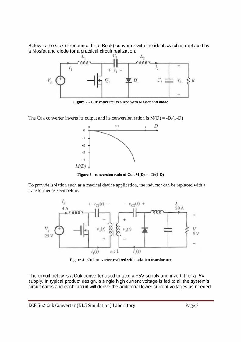
Below is the Cuk (Pronounced like Book) converter with the ideal switches replaced by a Mosfet and diode for a practical circuit realization.
Figure 2 - Cuk converter realized with Mosfet and diode
The Cuk converter inverts its output and its conversion ration is M(D) = -D/(1-D)
Figure 3 - conversion ratio of Cuk M(D) = - D/(1-D)
To provide isolation such as a medical device application, the inductor can be replaced with a transformer as seen below.
Figure 4 - Cuk converter realized with isolation transformer
The circuit below is a Cuk converter used to take a +5V supply and invert it for a -5V supply. In typical product design, a single high current voltage is fed to all the system’s circuit cards and each circuit will derive the additional lower current voltages as needed.

ECE 562 Cuk Converter (NL5 Simulation) Laboratory Page 4
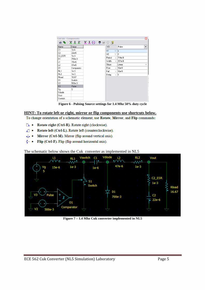
Implement the schematic below (minus the controller and feedback parts) to set up a ‘standard’ Cuk converter topology in NL5.
Figure 5 - 1.4 Mhz Cuk converter
To implement the schematic shown above in NL5 use the component values listed below. It should look like Figure 7 (below) when complete.
Vg is a DC voltage source (VDC) from the source library. It needs to be set for 5 volts. L 1 is an ideal inductor from the library. Set to 15 µH. RL1 is an ideal resistor from the library simulating the resistance of L 1. Set to 1 mΩ. C1 is an ideal capacitor from the library. Set to 1 µF. L 2 is an ideal inductor from the library. Set to 47 µH. RL2 is an ideal resistor from the library simulating the resistance of L 2. Set to 1 mΩ. D1 is an ideal diode from the library. Set to 700 mV (diode drop). C2 is an ideal capacitor from the library. Set to 22 µF. O1 is an ideal comparator used to turn the switch S1 on and off. By varying the width of
V3 below, its output will act as a Pulse Width Modulator. S1 is a voltage controlled switch, a standard component in the library. V2 is 0.5 volt reference for the Schmitt trigger comparator O1. Set V2 to 500 mV. V3 is Pulsing source. Set to values listed below using the components editing window.
This sets it to a switching frequency of ~1.4 MHz with a 50% duty cycle.
ECE 562 Cuk Converter (NL5 Simulation) Laboratory Page 5
Figure 6 - Pulsing Source settings for 1.4 Mhz 50% duty cycle
HINT: To rotate left or right, mirror or flip compo nents use shortcuts below.
The schematic below shows the Cuk converter as implemented in NL5
Figure 7 – 1.4 Mhz Cuk converter implemented in NL5

ECE 562 Cuk Converter (NL5 Simulation) Laboratory Page 6
Set the transient simulation parameters (Transient->Settings pull down menu) to those shown below:
Figure 8 - Transient settings for simulation
Now run the transient response simulation. The results should look as below:
Figure 9 - simulation results for schematic above
QUESTION 1: How long does it take the converter to reach steady state? What is the output voltage of the converter at steady state? Verify your results mathematically. What is the output voltage ripple?

ECE 562 Cuk Converter (NL5 Simulation) Laboratory Page 7
First select (highlight) V3 on the schematic view to allow the V3 parameters to be sweeped. Now, select from the pull down menu item Tool->Script and set up to run the pulse width from 71 nS to 710 nS to see the effects of varying duty cycle on the converter. For future sweeps of a components values, remember to always select the component on the schematic and then its name will show up on the sweep list.
Figure 10 - Script settings to varying Cuk converter duty cycle
Now press the blue arrow on the Tools-Script screen to start the simulations. The results should look like the window below.
Figure 11 - Cuk converter's output with varying duty cycles

ECE 562 Cuk Converter (NL5 Simulation) Laboratory Page 8
QUESTION 2: How does the output voltage of the converter vary with increasing switch duty cycle? Does the converter follow the conversion ratio M(D) = - D/(1-D)? How does increasing the duty cycle affect the settling time of the converter? Now clear all the data traces from the Transient Display window. Hint: To clear all the traces, select Transient->Data pull down menu, select the ‘storage’ tab and click on the black middle left ‘X’ to delete all data traces from the display.
Figure 12 - Select Transient ->Data then Storage tab to get screen to clear the data
Now look at the current waveform of L1 by applying a current marker.
Figure 13 - Current measurement of L1
QUESTION 3: What is the peak operating current now? What is the operating mode of the converter (remember that you can observe this by zooming in and determining if the sign of the current reverses)? Also, verify the mode mathematically.

ECE 562 Cuk Converter (NL5 Simulation) Laboratory Page 9
Now look at the current waveform of L2 by applying a current marker to it.
Figure 14 - Current waveform of L2
QUESTION 4: Does the current waveform of L2 show a continuous or discontinuous mode of operation? Now set the Transient Data to display V(Rload) and swept the Rload from 16.67 to 1600 ohms in 100% step increments using the script feature.
Figure 15 - Transient data set to display V(load)

ECE 562 Cuk Converter (NL5 Simulation) Laboratory Page 10
Figure 16 - Script-> Tools set up to sweep load from 16.67 to 1600 ohms
The output should look like the figure below.
Figure 17 - V(Rload) output when R is sweeped from 16.67 to 1600 ohms
QUESTION 5: What happen to the output voltage with an increase of the load resistance? Does the output ripple voltage increase or decrease with increasingly loading (lower R)?

ECE 562 Cuk Converter (NL5 Simulation) Laboratory Page 11
Now clear all the data and set Rload back to 16.67 ohms. Place a voltage marker on the load resistor (Rload).
Figure 18 - Setting for sweeping the ESR of C2
Figure 19 - Output voltage ripple when C2 ESR is sweeped from 1 mΩ to 10 Ω
QUESTION 6: Approximately what is the maximum equivalent series resistance C2 can have to keep the output ripple voltage below 150mV?

ECE 562 Cuk Converter (NL5 Simulation) Laboratory Page 12
Clear the data traces. Add a series resistor (Rswitch) to simulate series resistance of the switch. Add two wattmeters to measure the input power from the source and the power delivered into the load resistor. (Hint: Wattmeter is under the ‘W’ component list) HINT : The watt meter can measure both current and voltage. The power can be derived using by multiply current times voltage as a trace function. (IE: V(W1) * I(W1) )
Figure 20 - Wattmeter description from page 383 of NL5 manual
The schematic below shows what the NL5 schematic should look like with the addition of two wattmeters and the addition of a resistor to simulate switch resistance.
Figure 21 - Component list with addition of switch resistance and watt meters to measure efficiency

ECE 562 Cuk Converter (NL5 Simulation) Laboratory Page 13
Figure 22 - Cuk converter with addition of series switch resistance (Rswitch) and two wattmeters (W1 & W2) Delete other data traces by selecting the black ‘X’ and then add a trace for P(W2) and P(W1) to measure the output and input power of the Cuk converter.
Figure 23 - Adding traces for P(W1) and P(W2) to measure input and output power of converter to calculate
efficiency Run the transient response.

ECE 562 Cuk Converter (NL5 Simulation) Laboratory Page 14
Figure 24 - Transient respsonse of the input and output power for the Cuk converter
QUESTION 7: Using the input and output power measurements, what is the efficiency of the Cuk converter at this operating point? Now sweep the switch resistance from 100mΩ to 3Ω.
Figure 25 - Parameters to sweep the switch resistance from 100mΩ to 3Ω.

ECE 562 Cuk Converter (NL5 Simulation) Laboratory Page 15
Figure 26 - Output power of converter with switch resistance swepted from 100mΩ to 3Ω.
QUESTION 8: What happens to the efficiency of the Cuk converter as the switch resistance increases? Additional reading:
[1] Control System Design , R Tymerski, www.ece.pdx.edu/~tymerski/ece451/Tymerski_Rytkonen.pdf


![A Single Stage Three Phase Inverter Based on Cuk ... · In [9], the boost-inverter topology is used to build a single-phase single power stage fuel cell system with a backup battery](https://img.pdfslide.us/doc/110x75/5fc12026142d6f1a0f0de0f4/a-single-stage-three-phase-inverter-based-on-cuk-in-9-the-boost-inverter.jpg)


![An Efficient Bridge-Less Power Factor Correction Tapped ... · Cuk converter topology is generally a converter with lesser efficiency, ... TI-flyback [12], TI-cascaded boost [12];](https://img.pdfslide.us/doc/110x75/5b019fb47f8b9a84338e6c9c/an-efficient-bridge-less-power-factor-correction-tapped-converter-topology-is.jpg)