Embed Size (px)
Citation preview

3812 OPTICS LETTERS / Vol. 34, No. 24 / December 15, 2009
Simulation study of surface-plasmon-resonanceelectro-optic light modulator based on a
polymer grating coupler
Wen-Kai Kuo* and Meng-Ting ChenDepartment of Electro-Optics Engineering, National Formosa University, 64 Wenhua Road, Huwei,
Yunlin, Taiwan 63208*Corresponding author: [email protected]
Received August 5, 2009; revised October 24, 2009; accepted November 6, 2009;posted November 12, 2009 (Doc. ID 114902); published December 7, 2009
An electro-optic light modulator design based on a grating-coupled surface-plasmon-resonance structure isnumerically investigated using finite-difference time-domain simulation. The thickness effect of a dielectriclayer acting as a waveguide on metal structures is investigated. The results show that the new structure hasmuch higher modulation index than the conventional one and can implement an electro-optic modulatorwith low operating voltage. © 2009 Optical Society of America
OCIS codes: 240.6680, 050.2770, 230.4110.
A surface plasmon is an electromagnetic wave propa-gating along the surface of a metal and dielectric in-terface. Under phase-matching or resonance condi-tions, the energy of the incident light wave can becoupled to the collective oscillation of free electronson the metal surface. This energy-transfer phenom-enon can be achieved with p-polarized light by usingeither a prism or a grating coupler [1]. The energytransferred for excitation of the surface-plasmonresonance (SPR) is observed as a rapid decrease inreflectivity. Since the SPR is highly sensitive tochanges in the refractive index on the metal surface,this technique has been extensively applied to bio-chemical sensing [2]; moreover, it has also played animportant role in optical modulators. Further, theSPR technique can be combined with an electro-optic(EO) polymer in order to implement a simple andhigh-speed optical modulator. This type of device wastheoretically described [3] and experimentally dem-onstrated later with different advancements [4–6].Recently, a new type of a modulator that uses a reso-nant metal grating to greatly improve the modula-tion index has been proposed and numerically stud-ied [7]. For the above modulators, prism coupling orthe Kretschmann (KR) configuration is used for excit-ing SPR. However, this configuration requires aprism with high refractive index and therefore re-sults in a noncompact and high-cost modulator.
A conventional grating coupler adapted for EOpolymer modulation purpose and the reflectivitycurves calculated as a function of the angle of inci-dence � are shown in Fig. 1. This result is obtained bythe EM Explorer, a 3D electromagnetic solver basedon the finite-difference time-domain (FDTD) method[8]. In this structure as shown in the inset of the fig-ure, a polymer layer with a thickness of 300 nm cov-ers a gold grating with a modulation height of 70 nmand a pitch of 710 nm. The incident laser beam has awavelength of 632.8 nm, and two polymer refractiveindices are 1.489 and 1.490. The results reveal thatthe FWHM of the reflectivity curve exceeds 3°, and a
nonsignificant resonance angle shift is observed on0146-9592/09/243812-3/$15.00 ©
increasing polymer refractive indices from 1.489 to1.490. Hence, this structure can achieve only a verylow modulation depth. A similar structure using a na-nopolymer dispersed liquid-crystal EO material withhigh EO coefficients has been proposed [9]. Our newgrating coupler structure is shown in Fig. 2. A similarstructure has been previously described [10], and animplementation of such a structure has been demon-strated [11]. In [10], a grating structure is directlyformed on a flat metal film; in [11], an elastomericgrating fabricated by the replica molding method isplaced on the surface of a metal film. In the presentstudy, the above structure is further modified by de-positing a dielectric layer on the metal surface tofunction as a waveguide to improve the modulationindex. A similar structure has been applied for exci-tation of the long-range SPR [12]; however, the thick-ness effect was not discussed. Through the thicknesscontrol, the new structure can be used to design anEO modulator with low operating voltage.
Fig. 1. (Color online) Schematic of the SPR EO modulatorbased on a conventional grating coupler structure and re-flectivity curves calculated as a function of the angle of in-cidence for two polymer refractive indices of 1.489 and
1.490.2009 Optical Society of America
December 15, 2009 / Vol. 34, No. 24 / OPTICS LETTERS 3813
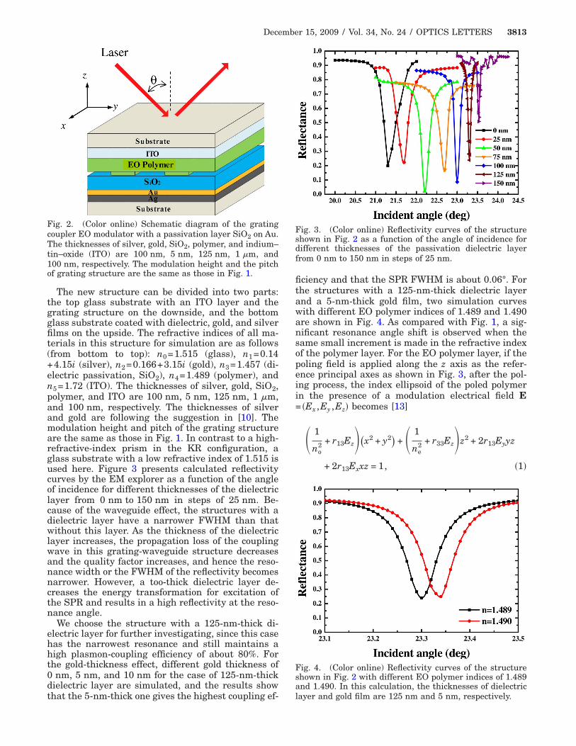
The new structure can be divided into two parts:the top glass substrate with an ITO layer and thegrating structure on the downside, and the bottomglass substrate coated with dielectric, gold, and silverfilms on the upside. The refractive indices of all ma-terials in this structure for simulation are as follows(from bottom to top): n0=1.515 (glass), n1=0.14+4.15i (silver), n2=0.166+3.15i (gold), n3=1.457 (di-electric passivation, SiO2), n4=1.489 (polymer), andn5=1.72 (ITO). The thicknesses of silver, gold, SiO2,polymer, and ITO are 100 nm, 5 nm, 125 nm, 1 �m,and 100 nm, respectively. The thicknesses of silverand gold are following the suggestion in [10]. Themodulation height and pitch of the grating structureare the same as those in Fig. 1. In contrast to a high-refractive-index prism in the KR configuration, aglass substrate with a low refractive index of 1.515 isused here. Figure 3 presents calculated reflectivitycurves by the EM explorer as a function of the angleof incidence for different thicknesses of the dielectriclayer from 0 nm to 150 nm in steps of 25 nm. Be-cause of the waveguide effect, the structures with adielectric layer have a narrower FWHM than thatwithout this layer. As the thickness of the dielectriclayer increases, the propagation loss of the couplingwave in this grating-waveguide structure decreasesand the quality factor increases, and hence the reso-nance width or the FWHM of the reflectivity becomesnarrower. However, a too-thick dielectric layer de-creases the energy transformation for excitation ofthe SPR and results in a high reflectivity at the reso-nance angle.
We choose the structure with a 125-nm-thick di-electric layer for further investigating, since this casehas the narrowest resonance and still maintains ahigh plasmon-coupling efficiency of about 80%. Forthe gold-thickness effect, different gold thickness of0 nm, 5 nm, and 10 nm for the case of 125-nm-thickdielectric layer are simulated, and the results show
Fig. 2. (Color online) Schematic diagram of the gratingcoupler EO modulator with a passivation layer SiO2 on Au.The thicknesses of silver, gold, SiO2, polymer, and indium–tin–oxide (ITO) are 100 nm, 5 nm, 125 nm, 1 �m, and100 nm, respectively. The modulation height and the pitchof grating structure are the same as those in Fig. 1.
that the 5-nm-thick one gives the highest coupling ef-
ficiency and that the SPR FWHM is about 0.06°. Forthe structures with a 125-nm-thick dielectric layerand a 5-nm-thick gold film, two simulation curveswith different EO polymer indices of 1.489 and 1.490are shown in Fig. 4. As compared with Fig. 1, a sig-nificant resonance angle shift is observed when thesame small increment is made in the refractive indexof the polymer layer. For the EO polymer layer, if thepoling field is applied along the z axis as the refer-ence principal axes as shown in Fig. 3, after the pol-ing process, the index ellipsoid of the poled polymerin the presence of a modulation electrical field E= �Ex ,Ey ,Ez� becomes [13]
� 1
no2 + r13Ez��x2 + y2� + � 1
ne2 + r33Ez�z2 + 2r13Eyyz
+ 2r13Exxz = 1, �1�
Fig. 3. (Color online) Reflectivity curves of the structureshown in Fig. 2 as a function of the angle of incidence fordifferent thicknesses of the passivation dielectric layerfrom 0 nm to 150 nm in steps of 25 nm.
Fig. 4. (Color online) Reflectivity curves of the structureshown in Fig. 2 with different EO polymer indices of 1.489and 1.490. In this calculation, the thicknesses of dielectric
layer and gold film are 125 nm and 5 nm, respectively.
3814 OPTICS LETTERS / Vol. 34, No. 24 / December 15, 2009
where no and ne are refractive indices of the poledpolymer for ordinary and extraordinary rays, respec-tively, and r13 and r33 are the EO tensor elements. Ifthe optical wave propagates along the y direction andonly the z-axis electric-field Ez is applied, the indexellipsoid in Eq. (1) can be simplified as an index el-lipse equation as
� 1
no2 + r13Ez�x2 + � 1
ne2 + r33Ez�z2 = 1. �2�
For the optical wave to excite the SPR, its polariza-tion direction is along z axis, and hence the corre-sponding refractive index change �n of the EO poly-mer induced by the voltage V applied across thepolymer is
�n =1
2ne
3r33
V
d, �3�
where d is the thickness of the EO polymer and V /dcorresponds to the electric-field Ez. Assuming that apolymer material with a high EO coefficient r33 of200 pm/V is used and the incident angle � is 23.28°,the reflectance as function of an applied voltage V isshown in Fig. 5. If the reflectivity bias point is set to50%, a modulation index of 0.5 can be achieved by alow operating voltage of 2.5 V. Since this new struc-ture is based on grating-coupled principle, the modu-lator operation is dependent on wavelength of the in-
Fig. 5. (Color online) Reflectance for a fixed incident anglewith increasing applied voltage between the metal and ITOlayers of the structure in Fig. 2.
cident light. Meanwhile, the modulator is a free-space type, the incident beam alignment accuracyshould be controlled to better than 0.01° to obtain theexpected performance. Regarding the device fabrica-tion, the different structures located on two sub-strates can be fabricated separately and then as-sembled together by using adhering or bondingtechnique. The EO polymer grating structure can befabricated by using simultaneous embossing and pol-ing method [14].
In conclusion, a new structure of a grating-coupledSPR EO modulator with good modulation perfor-mance has been numerically demonstrated using theFDTD simulation. The resonance angle of this newconfiguration shifts significantly for a small-index in-crement of 0.001 in the EO polymer grating struc-ture, and an EO modulator with low operating volt-age can be achieved.
The authors gratefully acknowledge the financialsupport provided by the National Science Council,Taiwan (NSCT) under grant NSC97-2221-E-150-020-MY3.
References
1. H. Raether, Surface Plasmons on Smooth and RoughSurfaces and on Gratings (Springer-Verlag, 1988).
2. J. Homola, S. S. Yee, and G. Gauglitz, Sens. ActuatorsB 56, 3 (1999).
3. J. S. Schildkraut, Appl. Opt. 27, 4587 (1988).4. O. Solgaard, F. Ho, J. I. Thackara, and D. M. Bloom,
Appl. Phys. Lett. 61, 2500 (1992).5. C. Jung, S. Yee, and K. Kuhn, Appl. Opt. 34, 946
(1995).6. X. Deng, X. Zheng, Z. Cao, Q. Shen, and H. Li, Appl.
Phys. Lett. 90, 151124 (2007).7. Z. Wu, R. L. Nelson, J. W. Haus, and Q. Zhan, Opt.
Lett. 33, 55 (2008).8. A. Taflove and S. C. Hagness, Computational
Electrodynamics: the Finite-Difference Time-DomainMethod, 3rd ed. (Artech House, 2005).
9. S. Massenot, R. Chevallier, J.-L. de Bougrenet de laTocnaye, and O. Parriaux, Opt. Commun. 275, 318(2007).
10. K. G. Muller, M. Veith, S. Mittler-Neher, and W. Knoll,J. Appl. Phys. 82, 4172 (1997).
11. A. Kocabas, A. Dana, and A. Aydinli, Appl. Phys. Lett.89, 041123 (2006).
12. S. Glasberg, A. Sharon, D. Rosenblatt, and A. A.Friesem, Appl. Phys. Lett. 70, 1210 (1997).
13. A. Yariv and P. Yeh, Optical Waves in Crystals (Wiley,1983).
14. O. Sugihara, M. Nakanishi, H. Fujimura, C. Egami,and N. Okamoto, Opt. Lett. 25, 1028 (2000).
![A High-Sensitivity and Broad-Range SPR Glucose Sensor ... · fiber grating sensors [1, 2] and surface plasmon resonance (SPR) sensors [3‒9]. SPR is a kind of optical excitation](https://img.pdfslide.us/doc/110x75/5fce014456e0375c9c4cba7f/a-high-sensitivity-and-broad-range-spr-glucose-sensor-fiber-grating-sensors.jpg)