Embed Size (px)
Citation preview

SIMULATION OF VARIOUS MODULATION STRATEGIES FOR
INDUCTION MOTOR DRIVE
A project report submitted to
CZECH TECHNICAL UNIVERSITY IN PRAGUE
In fulfilment of the requirements for the degree of
Master of Science
In
Electrical Engineering, Power Engineering and Management
By
Jigar Mehta
Guided By
Ing. Jan Bauer, Ph.D.
Electric Drives and Traction Department
May 2018

CERTIFICATE
This is to certify that research work embodied in this project report entitled “Simulation of
various modulation strategies for induction motor drive” was carried out by Mr. Jigar
Mehta, at Czech Technical University for the fulfilment of Master’s Degree to be awarded
by Czech Technical University. This research work has been carried out under my supervision
and is to my satisfaction.
Date: 24/05/2018
Place: Prague, Czech Republic
Ing. Jan Bauer, Ph.D.
Head of the Dept.
Assistant Professor
Dept. of Electric Drives and Traction
CTU, Prague.
Doc. Dr. Ing. Jan Kyncl Prof. Ing. Pavel Ripka
Head of the Dept. The Dean
Associate Professor Dept. of Electrical Engineering
Dept. of Electric Power Engineering CTU, Prague.
CTU, Prague.

DECLARATION
I hereby certify that I am the sole author of this report and that neither any part of this report
nor the whole of the report has been submitted for a degree to any other University or
Institution.
I certify that, to the best of my knowledge, my report does not infringe upon anyone’s copyright
nor violate any proprietary rights and that any ideas, techniques, quotations, or any other
material from the work of other people included in my report, published or otherwise, are fully
acknowledged in accordance with the standard referencing practices.
I declare that this is a true copy of my report, including any final revision, as approved by my
report review committee.
Date: 24/05/2018
Place: Prague, Czech Republic Signature and name of student
Verified by
Signature and name of supervisor

ACKNOWLEDGMENT
I am expressing my gratitude to everyone who supported me throughout this project named
“Simulation of various modulation strategies for induction motor drive”. I am thankful for
aspiring guidance, invaluably constructive criticism and friendly advice during the thesis work.
I am sincerely grateful for sharing their truthful and illuminating views on a number of issues
related to the project.
I express my warm thanks to Ing. Jan Bauer, Ph.D.; head of Electric Drives and Traction
Department, Czech Technical University, Prague for his support and guidance.
I am also thankful to the other faculty members of Electrical and Electronics Department, for
providing me relevant information and necessary clarifications.
Jigar Mehta

ABSTRACT
Developments in power electronics and semiconductor technology have lead improvements in
power electronic systems. PWM inverter-powered motor drives are more variable and offer in
a wide range better efficiency compared to fixed frequency motor drives. The lower order
harmonics can be eliminated and filtering out higher order harmonics are not much to worry
about. Thus, it reduces losses and increase performance and accuracy of the system.
In this thesis work, I am presenting Simulink models in Matlab simulation and comparing the
performance of a saturated induction motor drive for the basic three phase voltage source
inverter and for different PWM strategies such as Space Vector PWM and Sinusoidal PWM.
The complete system taken for simulation is a three-phase system, inverter based saturated
induction motor drive employing PWM techniques for inverter control. All the components of
the system are modelled as functionally decoupled Matlab-Simulink blocks, so that any
modifications for a new configuration of the system can be readily incorporated.
Main reason to pick this topic as a thesis work is, because of my field of interest, want to learn
more about Matlab simulation and use of the components such as comparators, goto-from etc.
Also Deeply getting knowledge about all modulation strategies and their interfacing with an
Induction motor used in today’s era is one the most interesting thing, to neglect most of the
lower order harmonics from any operating system. At the end of the thesis, compare the
outcomes of these modulation strategies to decide which PWM technique is most preferable
among them.

TABLE OF CONTENTS
CERTIFICATE ....................................................................................................................................... 1
DECLARATION .................................................................................................................................... 3
ACKNOWLEDGMENT ......................................................................................................................... 4
ABSTRACT ............................................................................................................................................ 5
LIST OF FIGURES ................................................................................................................................ 7
LIST OF TABLES .................................................................................................................................. 8
1. INTRODUCTION .......................................................................................................................... 9
2. MODULATION ........................................................................................................................... 11
2.1 CARRIER SIGNAL .................................................................................................................. 11
2.1.1 CLOCK OSCILLATOR ........................................................................................................ 12
2.1.1.1 REQUIREMENTS OF A CLOCK OSCILLATOR ........................................................... 13
3. TYPES OF MODULATION ........................................................................................................ 14
3.1 A.M (AMPLITUDE MODULATION) .................................................................................... 14
3.2 F.M (FREQUENCY MODULATION) .................................................................................... 14
3.3 P.W.M (PULSE WIDTH MODULATION) ............................................................................. 15
4. TYPES OF P.W.M TECHNIQUE ................................................................................................ 16
4.1 SINGLE PULSE WIDTH MODULATION (SINGLE PWM) .................................................... 16
4.2 MULTIPLE PULSE WIDTH MODULATION (MPWM) ........................................................... 17
4.3 SELECTED HARMONIC ELIMINATION PWM ...................................................................... 18
4.3.1 HARMONIC ELIMINATION THEORY ................................................................................. 18
4.3.2 LC-SECTION ............................................................................................................................ 20
4.4 MINIMUM RIPPLE CURRENT PWM ....................................................................................... 20
4.5 SINUSOIDAL PULSE WIDTH MODULATION (SPWM) ........................................................ 21
5.4.1 MODULATION INDEX OF SINUSOIDAL PWM .................................................................. 23
4.5.2 MODIFIED SINUSOIDAL PULSE WIDTH MODULATION ................................................ 24
4.6 SPACE VECTOR PULSE WIDTH MODULATION .................................................................. 25
5. INDUCTION MACHINE ............................................................................................................... 29
6. SIMULINK MODEL ...................................................................................................................... 33
6.1 INDUCTION MOTOR DRIVE .................................................................................................... 33
6.2 INDUCTION MOTOR FED BY AN INVERTER ...................................................................... 34
6.3 INDUCTION MOTOR FED BY PWM ....................................................................................... 37
6.4 INDUCTION MOTOR FED BY SINUSOIDAL PULSE WIDTH MODULATION.................. 40
6.5 INDUCTION MOTOR FED BY SPACE VECTOR PWM ......................................................... 43

7. CONCLUSION AND DISSCUSSION .......................................................................................... 47
7.1 FUTURE ASPECTS ..................................................................................................................... 47
8. BIBLIOGRAPHY ........................................................................................................................... 48
APPENDIX ........................................................................................................................................... 50
LIST OF FIGURES
FIGURE 2.1 CARRIER SIGNAL ...................................................................................................... 11
FIGURE 2.2 CONFIGURATIONS OF PIEZOELECTRICITY PROCESS ...................................... 12
FIGURE 2.3 A BASIC CRYSTAL OSCILLATOR (XO) CONFIGURATIONS ............................. 12
FIGURE 2.4 CRYSTAL STABILIZED RELAXATION OSCILLATOR ........................................ 13
FIGURE 3.1 AMPLITUDE MODULATION SIGNALS .................................................................. 14
FIGURE 3.2 FREQUENCY MODULATION SIGNALS ................................................................. 14
FIGURE 3.3 BLOCK DIAGRAM OF PWM SIGNAL GENERATION ........................................... 15
FIGURE 4.1 GENERATION OF SINGLE PULSE WIDTH MODULATION ................................. 16
FIGURE 4.2 GENERATION OF MULTIPLE PULSE WIDTH MODULATION ........................... 17
FIGURE 4.3 OUTPUT WAVEFORM OF VIRTUAL STAGE PWM CONTROL .......................... 19
FIGURE 4.4 THREE-PHASE SINUSOIDAL PWM: A) REFERENCE VOLTAGES (A, B, C) AND
TRIANGULAR WAVE, B) VAO, C) VBO, D) VCO, E) LINE-TO-LINE VOLTAGES ........................ 22
FIGURE 4.5 GENERATION OF MODIFIED SINUSOIDAL PULSE WIDTH MODULATION .. 24
FIGURE 4.6 THREE-PHASE VOLTAGE SOURCE PWM INVERTER......................................... 25
FIGURE 4.7 PHASE VOLTAGE SPACE VECTORS ...................................................................... 28
FIGURE 5.1 CLARKE TRANSFORMATION ................................................................................. 30
FIGURE 5.2 PARK TRANSFORMATION ....................................................................................... 30
FIGURE 5.3 TRANSFORMED FLUX ................................................................................................ 31
FIGURE 6.1 UNSATURATED INDUCTION MOTOR ................................................................... 33
FIGURE 6.2 IM FED BY VSI ............................................................................................................ 34
FIGURE 6.2.1 INPUT SUPPLY VOLTAGE ..................................................................................... 34
FIGURE 6.2.2 CLARKE TRANSFORMATION ................................................................................ 35
FIGURE 6.2.3 TORQUE .................................................................................................................... 35
FIGURE 6.2.4 MOTION .................................................................................................................... 35
FIGURE 6.2.5 STATOR CURRENTS ............................................................................................... 36
FIGURE 6.2.6 ROTOR CURRENTS ................................................................................................. 36
FIGURE 6.2.7 U,V COMPONENTS OF ROTOR CURRENTS ....................................................... 36

FIGURE 6.3 IM FED BY PWM INVERTER ...................................................................................... 37
FIGURE 6.3.1 INPUT SUPPLY VOLTAGE ..................................................................................... 37
FIGURE 6.3.2 CLARKE TRANSFORMATION .............................................................................. 38
FIGURE 6.3.3 TORQUE .................................................................................................................... 38
FIGURE 6.3.4 MOTION .................................................................................................................... 38
FIGURE 6.3.5 ROTOR CURRENTS ................................................................................................. 39
FIGURE 6.3.6 STATOR CURRENTS ............................................................................................... 39
FIGURE 6.4 IM FED BY SINUSOIDAL PWM INVERTER ........................................................... 40
FIGURE 6.4.1 CLARKE TRANSFORMATION .............................................................................. 40
FIGURE 6.4.2 TORQUE .................................................................................................................... 41
FIGURE 6.4.3 MOTION .................................................................................................................... 41
FIGURE 6.4.4 REVERSE PARK TRANSFORMATION ................................................................. 41
FIGURE 6.4.5 ROTOR CURRENTS ................................................................................................. 42
FIGURE 6.4.6 FLUX .......................................................................................................................... 42
FIGURE 6.4.6 U,V COMPONENTS OF ROTOR CURRENTS ....................................................... 42
FIGURE 6.5 IM FED BY SPACE VECTOR PWM INVERTER ...................................................... 43
FIGURE 6.5.1 INPUT SUPPLY VOLTAGE ..................................................................................... 43
FIGURE 6.5.2 COMPARE SUPPLY WITH REPEATING SEQUENCES ...................................... 44
FIGURE 6.5.3 OUTPUT VOLTAGE OF VSI ................................................................................... 44
FIGURE 6.5.4 CLARKE TRANSFORMATION .............................................................................. 44
FIGURE 6.5.5 TORQUE .................................................................................................................... 45
FIGURE 6.5.6 MOTION .................................................................................................................... 45
FIGURE 6.5.7 FLUX .......................................................................................................................... 45
FIGURE 6.5.8 STATOR CURRENTS ............................................................................................... 46
FIGURE 6.5.9 ROTOR CURRENTS ................................................................................................. 46
FIGURE 6.5.10 U,V COMPONENTS OF ROTOR CURRENTS ..................................................... 46
LIST OF TABLES
TABLE 1 PHASE VOLTAGE VALUES FOR DIFFERENT SWITCHING STATE ...................... 27
TABLE 2 PHASE VOLTAGE SPACE VECTORS. .......................................................................... 27

1. INTRODUCTION
Induction machines are the most widely used motors in industry. About 60% of the industrial
electric energy is converted into mechanical energy by means of pumps, fans, adjustable speed
drives and machine tools equipped with induction motors. Thus, considerable research efforts
have been focused on topics like modelling and parameter estimation of induction motors.
The machine parameters are not constant and depend on saturation and temperature. The
magnetic saturation effect is significant at motor start-up and near rated operating conditions.
Under saturated operation the voltage and/or current harmonics generated by the induction
motors become non negligible. These alter the static and dynamic performance of induction
motor drives, the efficiency as and the harmonic content of the supply mains for the
applications where the motors are directly connected to the power network.
For simulation study, different nonlinear models for saturated induction motors have been
elaborated based on the equivalent electric circuit approach. One of the first notable attempts
to model the saturated induction motors is represented by where an analog computer based
model has been developed. The model is built in d-q-0 reference frame and takes into account
the magnetic saturation of leakage flux path. The stator and rotor leakage inductances are both
separated into a saturable slot inductance and an end-winding inductance, whereas the end
winding portions are considered constants, the slot portions of leakage inductances are
considered saturable according to saturation factors. These saturation factors are previously
determined by experimental measurements on the motor which is to be modelled. The model
is quite complex and does not predict the current and/or voltage harmonics generated by the
motor under saturated operating conditions. Moreover, because the model structure contains
multiple closed loops, numerical convergence problems occur when digital computer
implementation is attempted.
In reference another model for saturated induction motors is proposed that accounts for
saturation in stator and rotor cores as well as in teeth. The model is built as an equivalent circuit
in d-q reference frame with variable reactance depending on saturation factors, previously
determined by finite-element methods or experimental measurements. Although the model is
quite simple, search coils have to be mounted in the motor air gap, stator slots and around the
stator core in order to determine proper values of model parameters. In addition, since the
model is in d-q frame (without using the 0 component) it is not possible to simulate the zero-
sequence components produced by saturation.
The model is built in a d-q-0 frame and uses variable stator and rotor inductances. These are
computed as functions of the variable air gap length and trigonometric functions taking into
account the fundamental and 3rd harmonic of the air gap flux. The model requires a large
number of parameters such as: geometrical dimensions of motor (air gap length, number of
rotor and stator slots, and the rotor stack length), equivalent turns ratio of stator and rotor
windings for the 3rd harmonic as well as air gap flux fundamental. Consequently, intensive and
time consuming measurements are required to build the model for a given motor.

In recent years, finite-element methods have been developed for magnetic analysis of motors,
but their main drawback is the inability to simulate the global system consisting of motor,
power converter and control system. Unlike mentioned models, the parameter values of
nonlinear model for delta connected saturated induction motors derived from the conventional
equations of the non-saturated induction machine can be tuned more easily. All the necessary
measurements are performed at the motor terminals. The proposed model gives good prediction
of line and stator winding currents under saturated conditions even for overvoltage operation
of the motor. [1]
Over the last decades, Power converters have become an enabling technology for a wide range
of industrial applications mainly due to higher efficiency and performance. Converter
topologies, such as the ac/ac matrix converter, cycloconverters, current-source inverters, load-
commutated inverters, dc/dc converters, dc/ac converters, and diode or thyristor based
rectifiers, cover a wide range of different nominal power applications. In particular, dc/ac
converters, commonly known as voltage-source inverters (VSIs), are used to power a wide
variety of applications in the nonstop energy-demanding society with high efficiency,
robustness, and economical cost and possibility to reach high nominal power with reduced
passive filters.
The rich diversity of industrial applications requires inverters that have very different power
ratings, output frequencies, semiconductor devices, number of phases, operate at different
voltage/current levels, and even have different types and number of dc-input sources (current
or voltage). Therefore, a wide range of different topologies have been developed over the years,
particularly in the last decade for medium-voltage applications, to cater the needs and fulfil the
specifications
Apart from well-known multilevel converter topologies, such as neutral-point-clamped (NPC),
flying-capacitor (FC), and cascaded H-bridge (CHB), in the last years, a great deal of new
inverter topologies have been introduced in industry, particularly in medium-voltage multilevel
converters, such as modular multilevel converter (MMC), five-level active NPC (5L-ANPC),
transistor-clamped converter (TCC), and stacked multicell. In addition, multiphase applications
have been gaining more and more attention due to a series of advantages, such as higher power
density, lower torque ripples, and fault-tolerant operation. As another example, open-end-
winding-fed drives also have different voltage-space vector distribution, and extension of
classic modulation methods is not straight forward. All these new power converters come along
with modulation challenges, which include additional voltage-space vectors and different
switching harmonics. [2]
A modulation technique generates the gate signals of power semiconductors of a power
converter obtaining a switched output waveform in such a way that the fundamental component
can be adjusted with an arbitrary magnitude, frequency, and phase, which are essential for the
proper control of the process fed by the inverter. Taking this fact into account, the pulse-width
modulation (PWM) is the modulation concept that has been the mainstream solution for
inverters. [2]

2. MODULATION
In power electronics, modulation is the process of varying one or more properties of a periodic
waveform, called the carrier signal, with a modulating signal that typically contains
information to be transmitted. [3]
Modulation is a technique in which message signal is transmitted to the receiver with the help
of carrier signal. Here in modulation, we combine both carrier signal and message signal. You
may get the doubt that what is the need of modulation. Just imagine that you have a paper
which contains the message and you would like to send it to your friend standing 40 feet from
your place. You can’t just through the paper to your friend because paper will not travel that
much distance but if you take small stone and cover the paper with it and through it to your
friend, it will definitely reach the target. In the same way, we need a carrier signal to transmit
our message. Sometimes, message signal is also called as modulating signal. The exact
definition of modulation is given below:
“Modulation is a process of message signal and modulating is varied according to the carrier
signal for transmission purpose. The message signal can varied in accordance to the carrier
signal that is in terms of angular or amplitude. So we are modulating the signal.”
Modulation Signal = Original Signal + Carrier Signal [3]
2.1 CARRIER SIGNAL
A method of generating a triangle waveform is to first use a clock oscillator to produce a square
wave and then use an integrator (low pass filter) to integrate the square wave into a triangle
wave it is called carrier signal which has been shown below in Figure 2.1. [3]
FIGURE 2.1 CARRIER SIGNAL

2.1.1 CLOCK OSCILLATOR
At the core of almost all modern digital systems is a high accuracy time base based on a crystal
oscillator. Crystal oscillators use the property of piezoelectricity to create waveforms with
excellent frequency accuracy based on the mechanical vibration of a precision machined
crystal.
Certain crystals, most notably quartz, exhibit the property of piezoelectricity. If force is applied
to the faces of a piece of crystal it causes a voltage to be generated from the crystal. Conversely,
if an electrical voltage is applied to a crystal it causes the crystal to deform mechanically, [5]
Thus Piezoelectricity converts a force applied to a crystal into an electric voltage and an applied
voltage into a mechanical deformation. This process is illustrated in figure 2.2.
FIGURE 2.2 CONFIGURATIONS OF PIEZOELECTRICITY PROCESS
If a crystal is placed into the feedback path of an amplifier circuit it begins to oscillate at a
frequency dependent primarily on the dimensions of the crystal. Figure 2.3 shows the basic
crystal oscillator configurations. [4]
FIGURE 2.3 A BASIC CRYSTAL OSCILLATOR (XO) CONFIGURATIONS

There are, basically, two categories of oscillators that are of interest to the electronics
engineers: Harmonic and relaxation. The former produce sinusoidal waveforms and contains
at least one active component that supplies power constantly to the passive components,
whereas relaxation oscillators produce non-sinusoidal waveform, such as rectangular pulses.
An oscillator is generally an amplifier operating with positive feedback in a manner whereby
an output is produced without any input signal. To achieve the desired frequency every
oscillator contains a frequency determining part, which may be an LC circuit, a phase shifting
RC network or a quartz crystal.
Figure 2.4 shows another approach. This circuit uses a standard RC-comparator multi vibrator
circuit with the crystal connected directly across the timing capacitor. Because the free running
frequency of the circuit is close to the crystal’s resonance, the crystal “steals” energy from the
RC, forcing it to run at the crystal’s frequency. It is important to ensure that enough current is
available to quickly start the crystal resonating while simultaneously maintaining an RC time
constant of appropriate frequency. Typically, the free running frequency should be set 5% to
10% above crystal resonance with a resistor feedback value calculated to allow about 100μA
into the capacitor-crystal network. This type of circuit is not recommended for use above a few
hundred kHz because of comparator delays. [5]
[5]
FIGURE 2.4 CRYSTAL STABILIZED RELAXATION OSCILLATOR
2.1.1.1 REQUIREMENTS OF A CLOCK OSCILLATOR
Clock oscillators must be reliable, easily reproducible and simple.

3. TYPES OF MODULATION
There are three types of modulation.
3.1 A.M (AMPLITUDE MODULATION)
In amplitude modulation, the amplitude (signal strength) of the carrier wave is varied in
proportion to the waveform being transmitted.
FIGURE 3.1 AMPLITUDE MODULATION SIGNALS
3.2 F.M (FREQUENCY MODULATION)
Frequency modulation (FM) is a modulation technique used in electronic communication, most
commonly for transmitting information via a radio carrier wave. [3]
FIGURE 3.2 FREQUENCY MODULATION SIGNALS

3.3 P.W.M (PULSE WIDTH MODULATION)
Pulse-width modulation (PWM) is a digital modulation technique in which the width of a pulse
carrier is changed according to the instantaneous value of the information signal. [3]
Pulse Width Modulation method is a fixed dc input voltage is given to the inverters and a
controlled ac output voltage is obtained by adjusting the on and off periods of the inverter
components. This is the most popular method of controlling the output voltage and in this
method is known as pulse width modulation (PWM CONTROL).
converters and motors, the PWM technique is mostly used to supply AC current to the load by
converting the DC current and it appears as a AC signal at load or can control the speed of
motors that run at high speed or low. The duty cycle of a PWM signal varies through analog
components, a digital microcontroller or PWM integrated circuits.
FIGURE 3.3 BLOCK DIAGRAM OF PWM SIGNAL GENERATION
Figure 3.3 shows the comparator gets the inputs as reference waveform (square wave) and a
carrier wave (triangular wave) is supply to the comparator to obtained PWM waveform.
Triangular wave is formed by op-amp driver. Triggering pulses are produced at the instant of
the carrier signal magnitude is greater than the reference signal magnitude. To turn-on the
IGBT switches, firing pulses are produced, the output voltage during the interval triangular
voltage wave stipulated the square modulating wave.
ADVANTAGES OF PWM TECHNIQUE:
• Output voltage can be controlled without other components.
• Output voltage can be controlled, lower order harmonics can be eliminated and filtering out
higher order harmonics by this filter requirements is minimized.
DISADVANTAGES OF PWM TECHNIQUE:
• The inverter switches are costly as they must have low turn off and turn on times. [6]

4. TYPES OF P.W.M TECHNIQUE
A number of PWM techniques are there to obtain variable voltage and frequency supply such
as,
(I) Single-Pulse Modulation
(II) Multiple-Pulse Modulation
(III) Selected Harmonic Elimination PWM (SHEPWM)
(IV) Minimum Ripple Current PWM
(V) Sinusoidal-Pulse PWM (SPWM)
(VI) Space Vector-Pulse PWM (SVPWM) [6]
4.1 SINGLE PULSE WIDTH MODULATION (SINGLE PWM)
In single pulse width modulation control technique only one pulse is present in every half cycle.
By adjusting the width of the single pulse we can control the output voltage of the inverter. The
gating signals are generated by comparing rectangular reference signal of amplitude (Ar) and a
triangular carrier wave (Ac), which has been shown in Figure 4.1.
This generated gating signal can be used to control the output of single phase full bridge
inverter. The fundamental frequency of the output voltage can be obtained by the frequency of
the reference signal.
For this technique the amplitude modulation index (M) can be defined as 𝑀=𝐴c𝐴𝑟, whereas the
instantaneous output voltage of the inverter can be given as V0= V1 (S1 – S4).
FIGURE 4.1 GENERATION OF SINGLE PULSE WIDTH MODULATION

The single pulse-width modulation converts the reference signal to the square wave signal.
This process is obtained by inter the reference signal to the zero-crossing circuit which consider
the positive part of the input signal is positive part of the output signal (square wave) and the
negative part of the input signal is negative part of the output signal as shown in Figure 4.1. [7]
4.2 MULTIPLE PULSE WIDTH MODULATION (MPWM)
The main drawback of single PWM technique is high harmonic content. The multiple PWM
technique is used in order to reduce the harmonic content. In this technique, a number of pulses
are given in each half cycle of output voltage. The gating signal are generated by comparing
the reference signal of the amplitude (Ar) with a triangular carrier wave (Ac) as shown Figure
4.2.
FIGURE 4.2 GENERATION OF MULTIPLE PULSE WIDTH MODULATION
The frequency (f0) of the output can be determined by the frequency of the reference signal.
By varying the modulation index the output voltage can be controlled. The number of pulses
‘P’ per half cycle is calculated by the carrier frequency (fc).

Number of pulses per half cycle is found by
𝑃=fc
2f0
= Mf
2
Where
𝑀𝑓 =𝑓𝑐
𝑓0, called as frequency modulation ratio.
The instantaneous output voltage of the inverter can be given as V0 = V1 (S1 – S4). [8]
The variation of modulation index (M) from 0 to 1 varies the pulse from 0 to π/p and the
output voltage from 0 to Ar (Vr). [7]
4.3 SELECTED HARMONIC ELIMINATION PWM
There are many popular methods are used to reduce the harmonics in order to get an effective
results. The popular methods for high switching frequency are Sinusoidal PWM and Space
Vector PWM. For low switching frequency methods are space vector modulation and selective
harmonic elimination. The SPWM technique has disadvantage that it cannot completely
eliminate the low order harmonics. Due to this it cause loss and high filter requirement is
needed. In Space Vector Modulation technique cannot be applied for unbalanced DC voltages.
SHE PWM technique uses many mathematical methods to eliminate specific harmonics such
as 5th, 7th, 11th, and 13th harmonics. The popular Selective Harmonic Elimination method is
also called fundamental switching frequency based on harmonic elimination Theory.
4.3.1 HARMONIC ELIMINATION THEORY
By applying Fourier series analysis, the output voltage can be obtained. Fourier series is an
infinite sum of trigonometric functions that are economically related. [6]
f (t)=a0+∑ 𝐶𝑛𝐶𝑜𝑠(2𝜋𝑛𝑓0 + 𝜙n)∞𝑛=0 (1)
Where,
n = Integer Multiple,
𝜙0= Initial Phase for nth Harmonic,
𝑎0 and 𝐶𝑛 = Fourier Co-efficients,
The output voltage equation derived for different voltage sources is given below:
v (t)= ∑4𝑉𝑑𝑐
𝑛𝜋
∞𝑛=1,3,5 ((𝑣1 Cos(n𝜙1)+ 𝑣2 Cos(n𝜙1)… 𝑣𝑠 Cos (n𝜙2)) Sin (nωt)) (2)
Where,
S = No. of dc sources connected per phase,
𝑣1, 𝑣2, 𝑣3= level of dc voltage 0 < Ѳ1< Ѳ2< Ѳ3… …< Ѳ𝑠< 𝜋
2 = Switching angles

For the above Fundamental peak voltage v (t), it is required to determine the switching angles
and some lower order harmonics of phase voltage are zero. Among no of switching angles one
is used for fundamental voltage selection and remaining (s-1) switching angles are needed to
eliminate lower order harmonics. For a balanced three phase system, triplen harmonics are
eliminated automatically by using line-line voltages so only non triplen odd harmonics are
present. To minimize harmonic distortion and to achieve adjustable amplitude of the
fundamental component, up to s-1 harmonic contents can be removed from the voltage
waveform. To keep the number of eliminated harmonics at a constant level, all switching angles
must satisfy the condition otherwise the total harmonic distortion (THD) increases
dramatically.
In order to achieve a wide range of modulation indexes with minimized THD for the
synthesized waveforms, a generalized selective harmonic modulation method is proposed,
which is called virtual stage PWM. An output waveform is shown in Figure 4.3. [8]
FIGURE 4.3 OUTPUT WAVEFORM OF VIRTUAL STAGE PWM CONTROL
Hence the relation between the fundamental voltage and maximum voltage is given by
modulation Index. It is given by m1, is the ratio of fundamental voltage v1 to the maximum
voltage.
The maximum voltage is given by
𝑣1𝑚𝑎𝑥 = 4
𝜋s𝑉𝑑𝑐
m = 𝜋𝑣1
4𝑠𝑉𝑑𝑐 (3)

Selective harmonic elimination control has been a widely researched alternative to traditional
pulse-width modulation technique. The elimination of specific low-order harmonics from a
given voltage/current waveform achieved by Selective Harmonic Elimination (SHE)
technique.
In this method there is no need to calculate the firing angles for placing notches. Here, the
lower order harmonics will be reduced by the dominant harmonics of same order generated in
opposite phase by sine PWM inverter. This is achieved by varying the phase angle of the carrier
wave of the sinusoidal Pulse Width Modulation (PWM) inverter, which generates the dominant
harmonics with sidebands very close to the amplitude of prominent voltage harmonics present
in the system but in opposite polarity.
In this method first, calculate the Total Harmonic Distortion (THD) for 3rd, 5th, 7th and 9th
order harmonics. Then calculate the amplitude of these order (3rd, 5th, 7th, and 9th) harmonics
with help of Total Harmonic Distortion (THD). After calculating amplitude, injecting the same
order of harmonics in opposite amplitude Thus the resultant disorder sine wave is compared
with triangular waveform and results in pulse are produced and will give to the switches. This
method is simple and easy implementation method for reducing the Total Harmonic Distortion
(THD).
4.3.2 LC-SECTION
Generally In inductor filter; the ripple feature is unswervingly comparative to the load
resistance (RL). On the other hand in a capacitor filter, it is unreliable inversely through the
load. Thus if we unite the inductor filter with the capacitor the ripple aspect will turn out to be
more or less autonomous of the load filter. It is also said to be as LC-section. In LC filter an
Inductor is connected in series with the load (RL). It offers high resistance path to the AC
mechanism and allows DC component to flow through the load (RL). The capacitor transverse
the load associated parallel and filter out if any AC constituent flowing through the inductance,
In this manner the AC component are filtered and a flat DC is supplied all the way through the
load. Here the distorted harmonics are removed and the smooth wave forms are obtained. [9]
4.4 MINIMUM RIPPLE CURRENT PWM
One disadvantage of the SHE PWM method is that the elimination of lower order harmonics
considerably boosts the next higher level of harmonics. Since the harmonic loss in a machine
is dictated by the RMS ripple current, it is the parameter that should be minimized instead of
emphasizing the individual harmonics.

4.5 SINUSOIDAL PULSE WIDTH MODULATION (SPWM)
The Sinusoidal PWM is a modulation technique in which a sinusoidal signal is compared with
the triangular signal, in which the frequency of triangular signal (ftri) is equals to the desired
sinusoidal output and the frequency of triangular signal gives the switching frequency of the
switches. [6]
It produces a sinusoidal waveform by filtering an output pulse waveform with varying width.
A high switching frequency leads to a better filtered sinusoidal output waveform. The
variations in the amplitude and frequency of the reference voltage change the pulse-width
patterns of the output voltage but keep the sinusoidal modulation.[10]
In three-phase SPWM, a triangular voltage waveform (VT ) is compared with three sinusoidal
control voltages (Va, Vb, and Vc), which are 120⁰ out of phase with each other and the relative
levels of the waveforms are used to control the switching of the devices in each phase leg of
the inverter.[10]
A six-step inverter is composed of six switches S1 through S6 with each phase output
connected to the middle of each inverter leg as shown in Figure 2.2. The output of the
comparators in Figure 2.1 form the control signals for the three legs of the inverter. Two
switches in each phase make up one leg and open and close in a complementary fashion.
That is, when one switch is open, the other is closed and vice-versa. The output pole voltages
Vao, Vbo, and Vco of the inverter switch between –Vdc/2 and +Vdc/2 voltage levels where Vdc is
the total DC voltage.
The peak of the sine modulating waveform is always less than the peak of the triangle carrier
voltage waveform. When the sinusoidal waveform is greater than the triangular waveform, the
upper switch is turned on and the lower switch is turned off. Similarly, when the sinusoidal
waveform is less than the triangular waveform, the upper switch is off and the lower switch is
on. Depending on the switching states, either the positive or negative half DC bus voltage is
applied to each phase. The switches are controlled in pairs ((S1; S4), (S3; S6), and (S5; S2)) and
the logic for the switch control signals is:
S1 is ON when Va>VT S4 is ON when Va<VT
S3 is ON when Vb>VT S6 is ON when Vb<VT
S5 is ON when Vc>VT S2 is ON when Vc<VT
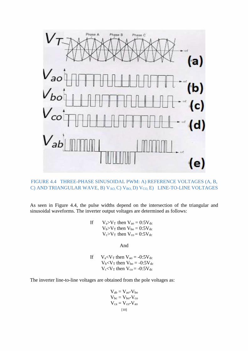
FIGURE 4.4 THREE-PHASE SINUSOIDAL PWM: A) REFERENCE VOLTAGES (A, B,
C) AND TRIANGULAR WAVE, B) VAO, C) VBO, D) VCO, E) LINE-TO-LINE VOLTAGES
As seen in Figure 4.4, the pulse widths depend on the intersection of the triangular and
sinusoidal waveforms. The inverter output voltages are determined as follows:
If Va>VT then Vao = 0:5Vdc
Vb>VT then Vbo = 0:5Vdc
Vc>VT then Vco = 0:5Vdc
And
If Va<VT then Vao = -0:5Vdc
Vb<VT then Vbo = -0:5Vdc
Vc<VT then Vco = -0:5Vdc
The inverter line-to-line voltages are obtained from the pole voltages as:
Vab = Vao-Vbo
Vbc = Vbo-Vco
Vca = Vco-Vao
[10]

5.4.1 MODULATION INDEX OF SINUSOIDAL PWM
The Fourier Series Expansion of a symmetrical square wave voltage with a peak magnitude of
Vdc/2 has a fundamental of magnitude 2Vdc/π. The maximum of the output voltage generated
by the SPWM method is Vdc/2. The modulation index is defined as the ratio of the magnitude
of output voltage generated by SPWM to the fundamental peak value of the maximum square
wave. The magnitude of o/p voltage depends on modulation index which is defined as,
“The ratio VT/VDC is called Modulation Index (Ma)”
It controls the harmonic content of the output voltage waveform. Thus, the maximum
modulation index of the SPWM technique is:
Modulation Index (Ma) = Amplitude of Sinusoidal Signal
Amplitude of Triangular signal
= 𝑉𝑝𝑤𝑚
𝑉𝑚𝑎𝑥−𝑆𝑖𝑥 𝑆𝑡𝑒𝑝
=
𝑉𝐷𝐶
22𝑉𝐷𝐶
𝜋
= 𝜋
4
= 0.7855 = 78.55%
Where VPWM is the maximum output voltage generated by a SPWM
Vmax- Six Step is the fundamental peak value of a square wave. [10]
ADVANTAGES
Controlled inverter output voltage
Reduction of harmonics
DISADVANTAGES
Increase of switching losses due to high PWM frequency
Reduction of available voltage
EMI problems due to high-order harmonics [6]

4.5.2 MODIFIED SINUSOIDAL PULSE WIDTH MODULATION
When considering sinusoidal PWM waveform, the pulse width does not change significantly
with the variation of modulation index. The reason is due to the characteristics of the sine wave.
Hence this sinusoidal PWM technique is modified so that the carrier signal is applied during
the first and last 600 intervals per half cycle as shown in Figure 4.5.
FIGURE 4.5 GENERATION OF MODIFIED SINUSOIDAL PULSE WIDTH
MODULATION
The fundamental component is increased and its harmonic characteristics are improved. The
main advantages of this technique is increased fundamental component, improved harmonic
characteristics, reduced number of switching power devices and decreased switching losses.
ADVANTAGES OF PWM
1. The output voltage control with method can be obtained without any additional
components
2. With this method, lower order harmonic can be eliminated or minimized along with
its output voltage control.
3. It reduces the filtering requirements [11]

4.6 SPACE VECTOR PULSE WIDTH MODULATION
The space vector PWM (SVM) method is an advanced computation-intensive PWM method
and is possibly the best method among the all PWM techniques for variable frequency drive
application. Because of its superior performance characteristics, it has been finding wide spread
application in recent years.
There are various variations of SVM that result in different quality and computational
requirements. One major benefit is in the reduction of total harmonic distortion (THD) created
by the rapid switching inherent to this PWM algorithm. [13]
It is an algorithm for the control of pulse width modulation (PWM). SVPWM is used for
producing of alternating current (AC) waveforms. It is frequently used to drive 3-phase AC
powered motors at variable speed from DC power. Various variations of SVPWM that result
in different quality and computational requirements. The development is in the reduction of
total harmonic distortion (THD) created by the rapid switching inherent to these algorithms.
Space vector modulation is a PWM regulator algorithm for multi-phase AC generation. The
reference signal is sampled frequently, after each sample, non-zero active switching vectors
adjacent to the reference vector and one or more of the zero switching vectors are preferred for
the suitable fraction of the sampling period in order to integrate the reference signal as the
average of the used vectors.
PRINCIPLE OF SPACE VECTOR PWM:
The circuit model of a typical three-phase voltage source PWM inverter is shown in Fig. 4.6,
S1 to S6 are the six power switches that shape the output, which are controlled by the switching
variables a, a’, b, b’, c and c’. When an upper IGBT is switched on, i.e., when a, b or c is 1, the
corresponding lower IGBT is switched off, i.e., the corresponding a’, b’ or c’ is 0.
FIGURE 4.6 THREE-PHASE VOLTAGE SOURCE PWM INVERTER
Space vector representation of the three-phase inverter output voltages is introduced next.
Space vector is defined as

Vs= (2/3) (Va+ a Vb+ a 2 Vc) (1)
Where,
A=exp (j 2π/3)
The space vector is a simultaneous representation of all the three-phase quantities. It is a
complex variable and is function of time in contrast to the phasors. Phase-to-neutral voltages
of a star-connected load are most easily found by defining a voltage difference between the star
point n of the load and the negative rail of the dc bus N. The following correlation then holds
true,
VA= Va+VnN
VB= Vb+VnN (2)
VC= Vc+VnN
Since the phase voltages in a start connected load sum to zero, summation of equation (2)
yields
VnN= (1/3) (VA+VB+ VC) (3)
Substitution of (3) into (2) yields phase -to-neutral voltages of the load in the following form:
Va = (2/3) VA-(1/3) (VB+ VC)
Vb = (2/3) VB-(1/3) (VA+ VC)
Vc = (2/3) VC-(1/3) (VB+ VA)
Phase voltages are summarized in Table 1 and their corresponding space vectors are listed in
Table 2.
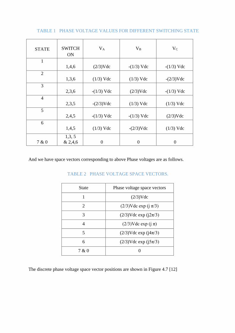
TABLE 1 PHASE VOLTAGE VALUES FOR DIFFERENT SWITCHING STATE
STATE
SWITCH
ON
VA
VB
VC
1
1,4,6
(2/3)Vdc
-(1/3) Vdc
-(1/3) Vdc
2
1,3,6
(1/3) Vdc
(1/3) Vdc
-(2/3)Vdc
3
2,3,6
-(1/3) Vdc
(2/3)Vdc
-(1/3) Vdc
4
2,3,5
-(2/3)Vdc
(1/3) Vdc
(1/3) Vdc
5
2,4,5
-(1/3) Vdc
-(1/3) Vdc
(2/3)Vdc
6
1,4,5
(1/3) Vdc
-(2/3)Vdc
(1/3) Vdc
7 & 0
1,3, 5
& 2,4,6
0
0
0
And we have space vectors corresponding to above Phase voltages are as follows.
TABLE 2 PHASE VOLTAGE SPACE VECTORS.
State Phase voltage space vectors
1 (2/3)Vdc
2 (2/3)Vdc exp (j π/3)
3 (2/3)Vdc exp (j2π/3)
4 (2/3)Vdc exp (j π)
5 (2/3)Vdc exp (j4π/3)
6 (2/3)Vdc exp (j5π/3)
7 & 0 0
The discrete phase voltage space vector positions are shown in Figure 4.7 [12]

FIGURE 4.7 PHASE VOLTAGE SPACE VECTORS
The major advantage of SVPWM method is from the fact that there is a degree of freedom of
space vector placement in a switching cycle. This improves the harmonic performance of this
method. [7]

5. INDUCTION MACHINE
Three-phase squirrel-cage type induction motors (IM) have been favoured because of their
good self-starting capability, simple and rugged structure, low cost and reliability, etc. These
motors are commonly utilized in the industries from the capacity of several kilowatts to
thousands of kilowatt as the driving units for fans, pumps, and compressors.
Usually, the motors are maintained periodically. However, when the ground fault occurs at the
motor terminal, a serious damage may be brought to the motor. In the worst case, the motor is
unable to start after the restoration of the power supply. Also it has been known that re-
switching the supply onto a squirrel cage induction motor can result in the production of large
negative torque transients. Therefore, it is significant to understand the transient phenomena
under abnormal conditions for the optimal design of induction motors.
In this method of analysis, it is assumed that the effect of saturation due to either the
magnetizing inductance or the leakage inductances is negligible. Using this assumption, the
values of the magnetizing inductance, stator leakage, and rotor leakage inductances are
constant and thus do not vary with the magnetizing current. Also several methods have been
developed for the modelling of saturation effects in induction machines. For example in
induction motor with saturable leakage reactance is modelled. [14]
SYSTEM OF EQUATIONS
The voltage equation can be written for each winding i:
𝑢𝑖 = 𝑅𝑖*𝑖𝑖 + 𝑑𝜓𝑖
𝑑𝑡
Magnetic flux 𝜓i can be expressed:
𝜓𝑖 = 𝐿𝑖𝑖*𝑖𝑖 + ∑ 𝑀𝑖𝑗(𝑗≠1) ∗ 𝑖𝑗(𝑗≠𝑖)𝑐𝑖,𝑗=𝑎
Angle q - mutual position between stator and rotor depends on mutual angular velocity
between them
Ѳ = ∫ 𝜔𝑑𝑡
Usually, three stator voltages, three rotor voltages and angular velocity are chosen. In order to
reduce the number of electrical equations, the Clarke and Park transformations are
established.

CLARKE TRANSFORMATION
It is assumed for the stator and rotor currents:
𝑖𝑆𝑎 + 𝑖𝑆𝑏+ 𝑖𝑆𝑐 = 0 𝑖𝑅𝑎 + 𝑖𝑅𝑏+ 𝑖𝑅𝑐 = 0
The three-phase windings system abc is transformed into the system αβ of two windings that
are perpendicular, so that the mutual inductance is zero. This transformation is called the 3/2
transformation or Clarke transformation.
𝑖𝑆∝ = 𝑖𝑆𝑎 , 𝑖𝑆𝛽 = 1
√3*𝑖𝑆𝑎 +
2
√3*𝑖𝑆𝑏
FIGURE 5.1 CLARKE TRANSFORMATION
PARK TRANSFORMATION
The two windings system αβ is transformed into another system UV that rotates with angular
speed ωk.
𝑖𝑆𝑢 = 𝑖∝*Cos Ѳ𝑘 + 𝑖𝛽*SinѲ𝑘 𝑖𝑆𝑣 = -𝑖∝*SinѲ𝑘 + 𝑖𝛽*CosѲ𝑘
FIGURE 5.2 PARK TRANSFORMATION

TRANFORMED VOLTAGE EQUATION
The set of voltage equations after the Park transformation into the general system uv that
rotates with angular speed ωk:
𝑢𝑆𝑢 = 𝑅𝑆*𝑖𝑆𝑢 + 𝑑𝜓𝑆𝑢
𝑑𝑡 - ωk*𝜓𝑆𝑣
𝑢𝑆𝑣 = 𝑅𝑆*𝑖𝑆𝑣 + 𝑑𝜓𝑆𝑣
𝑑𝑡 - ωk*𝜓𝑆𝑢
𝑢𝑅𝑢 = 𝑅𝑅*𝑖𝑅𝑢 + 𝑑𝜓𝑅𝑢
𝑑𝑡 – (ωk-ω)*𝜓𝑅𝑣
𝑢𝑅𝑣 = 𝑅𝑅*𝑖𝑅𝑣 + 𝑑𝜓𝑅𝑣
𝑑𝑡 + (ωk-ω)*𝜓𝑅𝑢
The rotor voltages uSu and uSv are zeros for a squirrel cage induction machine.
TRANSFORMED FLUX EQUATIONS
The imagination of the flux in an induction machine can be as depicted in the picture.
Then, the flux equations can be written:
𝜓𝑆𝑢= LS*iSu + Lh*iRu 𝜓𝑆𝑣= LS*iSv + Lh*iRv
𝜓𝑅𝑢= LS*iRu + Lh*iSu 𝜓𝑅𝑣= LS*iRv + Lh*iSv
FIGURE 5.3 TRANSFORMED FLUX
The electromagnetic torque Te can be expressed as:
Te = 3
2* pp *
𝐿ℎ
𝐿𝑅 * (𝜓𝑅𝑢 ∗ 𝑖𝑆𝑣 + 𝜓𝑅𝑣 ∗ 𝑖𝑆𝑢)
pp ... number of pole-pairs

The motion equation is usually written as:
Te - TL = J * 𝑑𝜔𝑚
𝑑𝑡
ω = pp * 𝜔𝑚
Where, TL is the load torque, J is the moment of inertia, 𝜔𝑚 is the mechanical angular speed and
ω is the electrical angular frequency.
There are several ways, how to form the system of equations that describes the model of an
induction machine. It depends on a selection on state quantities. Let's select the stator current
is, the rotor flux 𝜓𝑅 and mechanical rotational speed 𝜔𝑚.
The state quantities have to be in the simulation equations in form of differential coefficient –
they will be integrated and therefore the system of equations will be stable.

6. SIMULINK MODEL
6.1 INDUCTION MOTOR DRIVE
FIGURE 6.1 UNSATURATED INDUCTION MOTOR

6.2 INDUCTION MOTOR FED BY AN INVERTER
FIGURE 6.2 IM FED BY VSI
FIGURE 6.2.1 INPUT SUPPLY VOLTAGE
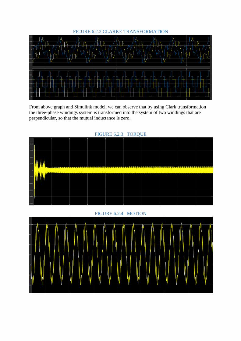
FIGURE 6.2.2 CLARKE TRANSFORMATION
From above graph and Simulink model, we can observe that by using Clark transformation
the three-phase windings system is transformed into the system of two windings that are
perpendicular, so that the mutual inductance is zero.
FIGURE 6.2.3 TORQUE
FIGURE 6.2.4 MOTION

FIGURE 6.2.5 STATOR CURRENTS
FIGURE 6.2.6 ROTOR CURRENTS
FIGURE 6.2.7 U,V COMPONENTS OF ROTOR CURRENTS

6.3 INDUCTION MOTOR FED BY PWM
FIGURE 6.3 IM FED BY PWM INVERTER
FIGURE 6.3.1 INPUT SUPPLY VOLTAGE

FIGURE 6.3.2 CLARKE TRANSFORMATION
From above graph and Simulink model, we can observe that by using Clark transformation
the three-phase windings system is transformed into the system of two windings that are
perpendicular, so that the mutual inductance is zero.
FIGURE 6.3.3 TORQUE
FIGURE 6.3.4 MOTION

FIGURE 6.3.5 ROTOR CURRENTS
FIGURE 6.3.6 STATOR CURRENTS

6.4 INDUCTION MOTOR FED BY SINUSOIDAL PULSE WIDTH
MODULATION
FIGURE 6.4 IM FED BY SINUSOIDAL PWM INVERTER
FIGURE 6.4.1 CLARKE TRANSFORMATION
From above graph and Simulink model, we can observe that by using Clark transformation
the three-phase windings system is transformed into the system of two windings that are
perpendicular, so that the mutual inductance is zero.

FIGURE 6.4.2 TORQUE
FIGURE 6.4.3 MOTION
FIGURE 6.4.4 REVERSE PARK TRANSFORMATION

FIGURE 6.4.5 ROTOR CURRENTS
FIGURE 6.4.6 FLUX
FIGURE 6.4.6 U,V COMPONENTS OF ROTOR CURRENTS

6.5 INDUCTION MOTOR FED BY SPACE VECTOR PWM
FIGURE 6.5 IM FED BY SPACE VECTOR PWM INVERTER
FIGURE 6.5.1 INPUT SUPPLY VOLTAGE

FIGURE 6.5.2 COMPARE SUPPLY WITH REPEATING SEQUENCES
FIGURE 6.5.3 OUTPUT VOLTAGE OF VSI
FIGURE 6.5.4 CLARKE TRANSFORMATION
From above graph and Simulink model, we can observe that by using Clark transformation
the three-phase windings system is transformed into the system of two windings that are
perpendicular, so that the mutual inductance is zero.
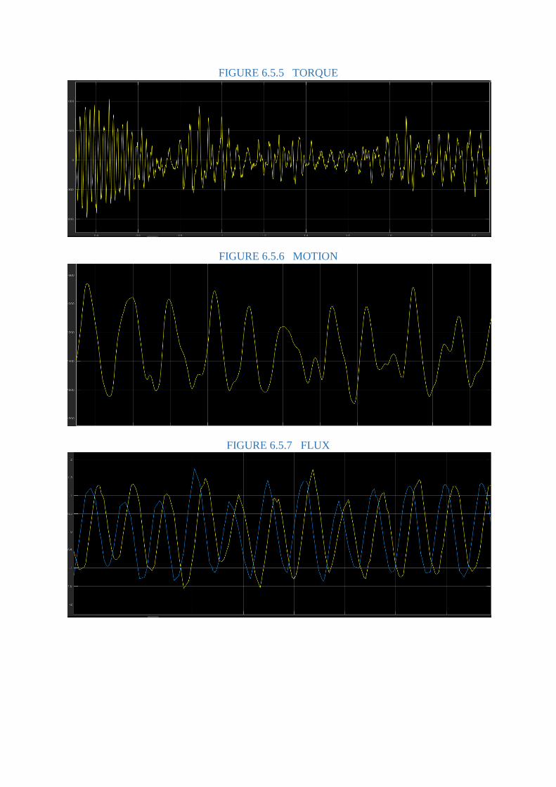
FIGURE 6.5.5 TORQUE
FIGURE 6.5.6 MOTION
FIGURE 6.5.7 FLUX

FIGURE 6.5.8 STATOR CURRENTS
FIGURE 6.5.9 ROTOR CURRENTS
FIGURE 6.5.10 U, V COMPONENTS OF ROTOR CURRENTS

7. CONCLUSION AND DISSCUSSION
Pulse Width Modulation is most preferable strategy used in each and every industrial applications.
Different Pulse Width Modulation technologies are accurate and they minimize switching losses. By
applying two different kind of Pulse Width Modulation strategies to the Induction machine, we
compare results which we got in the Matlab simulation so we can see the pros and cons of both the
strategies. At the end, we can choose the best strategy that we can apply and it is beneficial for
industrial use.
7.1 FUTURE ASPECTS
I would like to work on some hardware practical based on these different strategies fed to an Induction
Machine and how they affect all the parameters of the machine such as speed, torque, stator and
rotor currents. I also want to continue my work ahead in Research work.

8. BIBLIOGRAPHY
[1] Modelling and Simulation of Saturated Induction Motors in Phase Quantities. V.Donescu,
A.Charette, Members IEEE; Z.Yao, Senior Member, IEEE and VRajagopalan, Fellow, IEEE:
IEEE Transactions on Energy Conversion, Vol. 14, No. 3, September 1999
[2] The Essential Role and the Continuous Evolution of Modulation Techniques for Voltage-
Source Inverters in the Past, Present, and Future Power Electronics. Jose I. Leon, Leopoldo G.
Franquelo: IEEE transactions on industrial electronics, vol. 63, no. 5, may 2016.
[3] Pulse width modulation with using dc fan & pulse generator. Amar Pandey
[4] Clock Oscillator Basics. Cardinal Components Inc. Applications Brief No. A.N. 1005.
[5] Circuit Techniques for Clock Sources. Jim Williams: Linear Technology, Application Note
12, October 1985.
[6] Control of Induction Motor Drive using Space Vector PWM. Mohammed Abdul Khader
Aziz Biabani, Syed Mahamood Ali: International Conference on Electrical, Electronics, and
Optimization Techniques (ICEEOT) – 2016.
[7] A SURVEY AND STUDY OF DIFFERENT TYPES OF PWM TECHNIQUES USED IN
INDUCTION MOTOR DRIVE. Sandeep Kumar Singh, Harish Kumar, Kamal Singh, Amit
Patel: [IJESAT] International Journal of Engineering Science & Advanced Technology,
Volume-4, Issue-1, 018-122.
[8] Selective Harmonic Elimination of Multilevel Inverter Using SHEPWM Technique
B. Ashok, A. Rajendran: International Journal of Soft Computing and Engineering (IJSCE)
ISSN: 2231-2307, Volume-3, Issue-2, May 2013.
[9] Selective Harmonic Elimination (SHE) for 3-Phase Voltage Source Inverter (VSI)
V. Karthikeyan, V. J. Vijayalakshmi, P. Jeyakumar: American Journal of Electrical and
Electronic Engineering, 2014, Vol. 2, No. 1, 17-20.
[10] MATLAB/SIMULINK IMPLEMENTATION AND ANALYSIS OF THREE PULSE-
WIDTH-MODULATION (PWM) TECHNIQUES. Phuong Hue Tran: Boise State University
May 2012.
[11] MODIFIED SINUSOIDAL PULSE WIDTH MODULATION (SPWM) TECHNIQUE
BASED CONTROLLER.
[12] V/F Speed Control of 3-phase Induction motor using Space Vector Modulation. Ms Priya
Subhash Raichrkar, Mr Asif Liyakat Jamadar: International Journal of engineering Research
and Technology (IJERT), ISSN: 2278-0181, Vol. 4 Issue 05, May-2015.
[13] Space Vector Modulation (SVM) Technique for PWM inverters. Amey Patil, Amey Khot,
Charudatt Awaghate, Srikant Pillai, Purushotam Kumar.

[14] A New Matlab Simulation of Induction Motor. Mohamad H. Moradi, Pouria G. Khorasani:
University of Bu Ali Sina, Department of Electrical Engineering, West Regional Electric Co,
Iran
APPENDIX
AC: Alternating Current
DC: Direct Current
VSI: Voltage-Source Inverters
NPC: Neutral-Point-Clamped
FC: Flying-Capacitor
CHB: Cascaded H-bridge
MMC: Modular Multilevel Converter
TCC: Transistor-Clamped Converter
A.M: Amplitude Modulation
F.M: Frequency Modulation
PWM: Pulse Width Modulation
SHEPWM: Selected Harmonic Elimination PWM
SPWM: Sinusoidal PWM
SVPWM: Space Vector PWM
THD: Total Harmonic Distortion
IM: Induction Motor