Embed Size (px)
Citation preview
External Use
TM
Simulation of Packaged
Component Electrical
Performance
FTF-SDS-F0024
A P R . 2 0 1 4
Neil Tracht | Package Design Manager
TM
External Use 1
Session Introduction
• Electrical Simulation of Package and Assembly
− The integrated circuit package is a crucial element in overall system
performance.
− Power and signal integrity within the package are essential for robust
system performance
− Freescale conducts extensive electrical simulation of the package and
assembly design to assure the performance of Freescale products
− This presentation will provide an overview of aspects of this modeling
and simulation for automotive and microcontroller packages
• Presentation by Neil Tracht – Manager, Wirebond Package Design
& Electrical Simulation
TM
External Use 2
Session Objectives
• After completing this session you will be able to:
− Describe methods for package parasitic extraction
− Name the types of electrical analysis preformed on IC packages
− Describe how the electrical performance of the IC package impacts
system performance
− Describe how package parasitics are incorporated into
Input Output Buffer Information Specification (IBIS) Models
TM
External Use 3
Agenda
• Package analysis tools
• Power and signal integrity
− PI/SI background
− Power supply noise example
− Signal integrity example
• Package design considerations
− Substrate
− Leadframe
− Wire diameter and wire material
− Current capacity
• Input Output Buffer Information Specification (IBIS) models
TM
External Use 4
Package Analysis Tools
TM
External Use 5
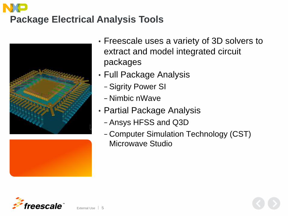
Package Electrical Analysis Tools
• Freescale uses a variety of 3D solvers to
extract and model integrated circuit
packages
• Full Package Analysis
− Sigrity Power SI
− Nimbic nWave
• Partial Package Analysis
− Ansys HFSS and Q3D
− Computer Simulation Technology (CST)
Microwave Studio
TM
External Use 6
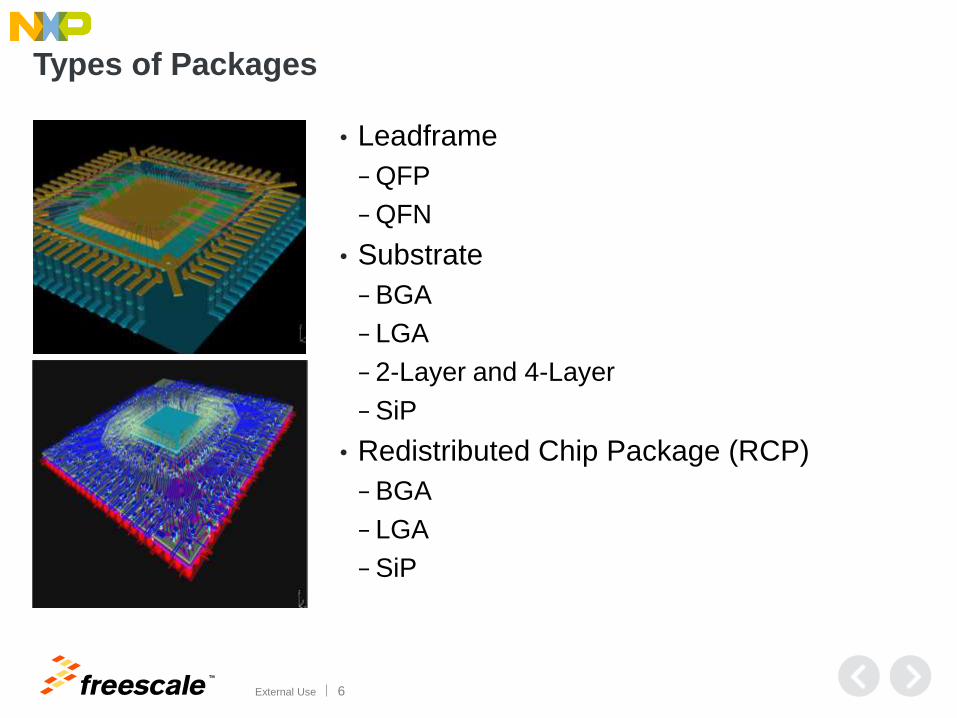
Types of Packages
• Leadframe
− QFP
− QFN
• Substrate
− BGA
− LGA
− 2-Layer and 4-Layer
− SiP
• Redistributed Chip Package (RCP)
− BGA
− LGA
− SiP

TM
External Use 7
Understanding Package
Parasitics
TM
External Use 8
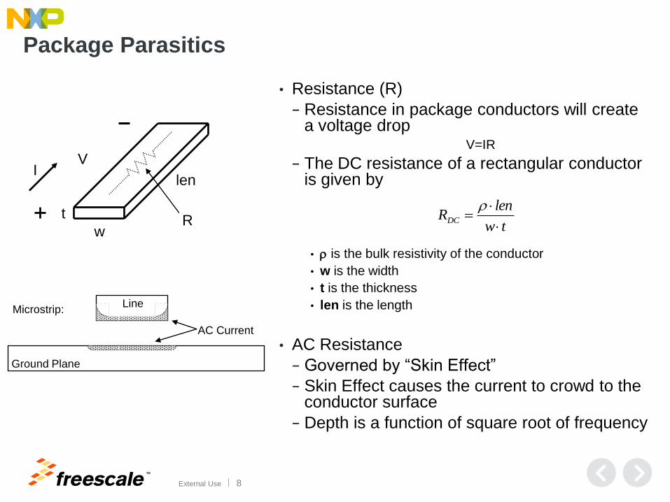
Package Parasitics
• Resistance (R)
− Resistance in package conductors will create a voltage drop
V=IR
− The DC resistance of a rectangular conductor is given by
• r is the bulk resistivity of the conductor
• w is the width
• t is the thickness
• len is the length
• AC Resistance
− Governed by “Skin Effect”
− Skin Effect causes the current to crowd to the conductor surface
− Depth is a function of square root of frequency
tw
lenRDC
rt
w
I V
len
R
Ground Plane
Line
AC Current
Microstrip:
TM
External Use 9
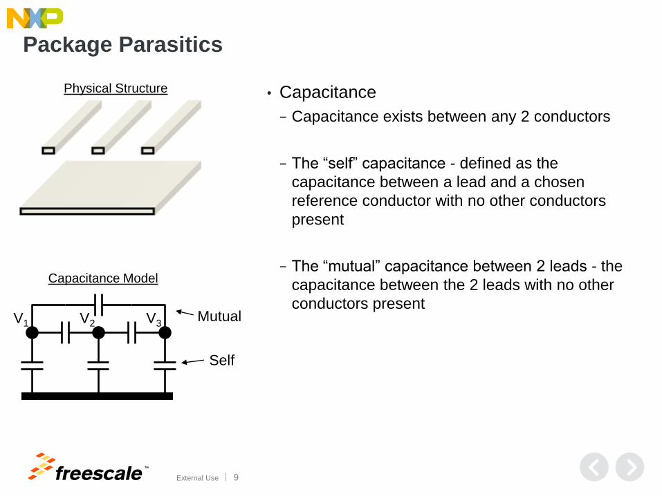
Package Parasitics
• Capacitance
− Capacitance exists between any 2 conductors
− The “self” capacitance - defined as the
capacitance between a lead and a chosen
reference conductor with no other conductors
present
− The “mutual” capacitance between 2 leads - the
capacitance between the 2 leads with no other
conductors present
Physical Structure
V1 V2 V3 Mutual
Self
Capacitance Model
TM
External Use 10
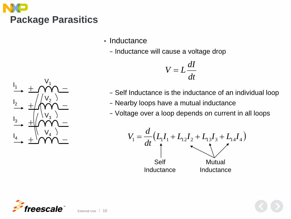
Package Parasitics
• Inductance
− Inductance will cause a voltage drop
− Self Inductance is the inductance of an individual loop
− Nearby loops have a mutual inductance
− Voltage over a loop depends on current in all loops
dt
dILV
V1
V2
V3
V4
I1
I2
I3
I4 414313212111 ILILILILdt
dV
Self
Inductance
Mutual
Inductance
TM
External Use 11
Package Design Considerations
TM
External Use 12
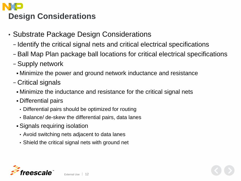
Design Considerations
• Substrate Package Design Considerations
− Identify the critical signal nets and critical electrical specifications
− Ball Map Plan package ball locations for critical electrical specifications
− Supply network
Minimize the power and ground network inductance and resistance
− Critical signals
Minimize the inductance and resistance for the critical signal nets
Differential pairs
• Differential pairs should be optimized for routing
• Balance/ de-skew the differential pairs, data lanes
Signals requiring isolation
• Avoid switching nets adjacent to data lanes
• Shield the critical signal nets with ground net
TM
External Use 13
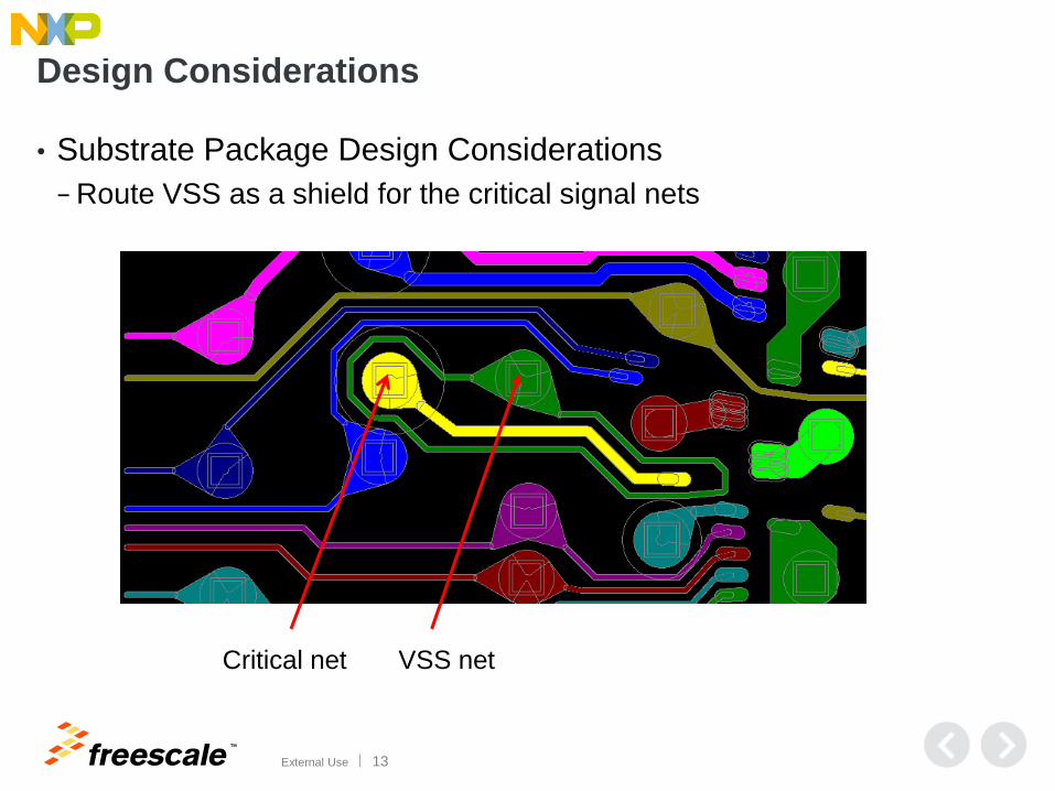
Design Considerations
• Substrate Package Design Considerations
− Route VSS as a shield for the critical signal nets
Critical net VSS net
TM
External Use 14
Design Considerations
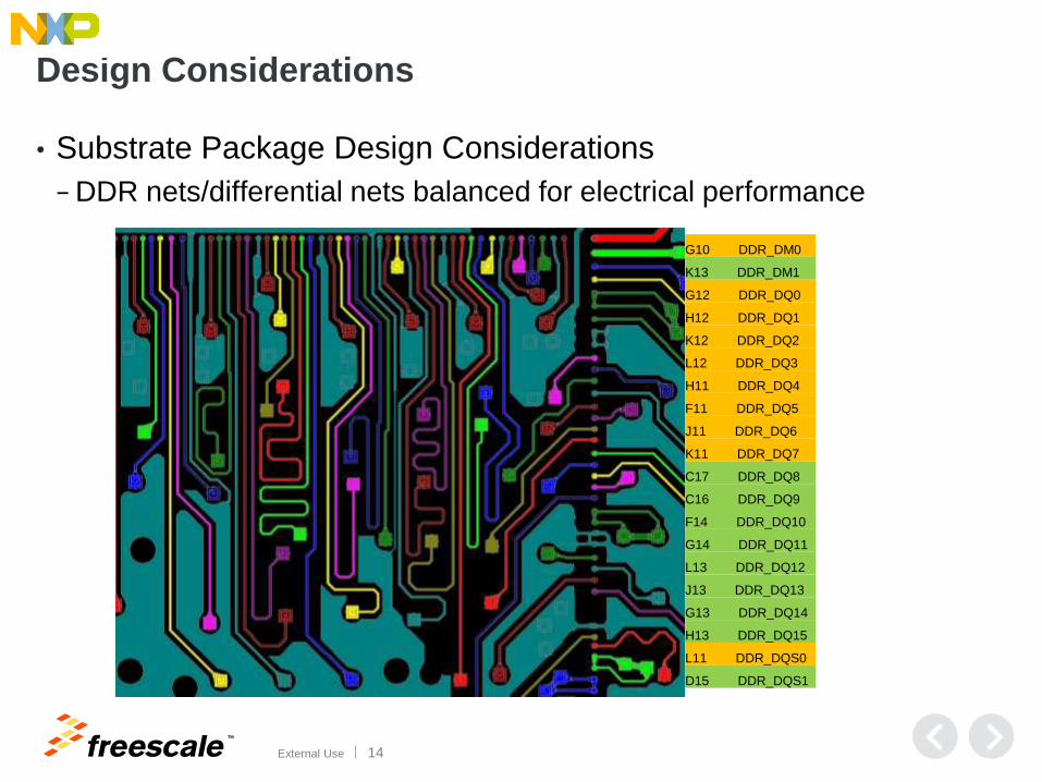
• Substrate Package Design Considerations
− DDR nets/differential nets balanced for electrical performance
G10 DDR_DM0
K13 DDR_DM1
G12 DDR_DQ0
H12 DDR_DQ1
K12 DDR_DQ2
L12 DDR_DQ3
H11 DDR_DQ4
F11 DDR_DQ5
J11 DDR_DQ6
K11 DDR_DQ7
C17 DDR_DQ8
C16 DDR_DQ9
F14 DDR_DQ10
G14 DDR_DQ11
L13 DDR_DQ12
J13 DDR_DQ13
G13 DDR_DQ14
H13 DDR_DQ15
L11 DDR_DQS0
D15 DDR_DQS1
TM
External Use 15
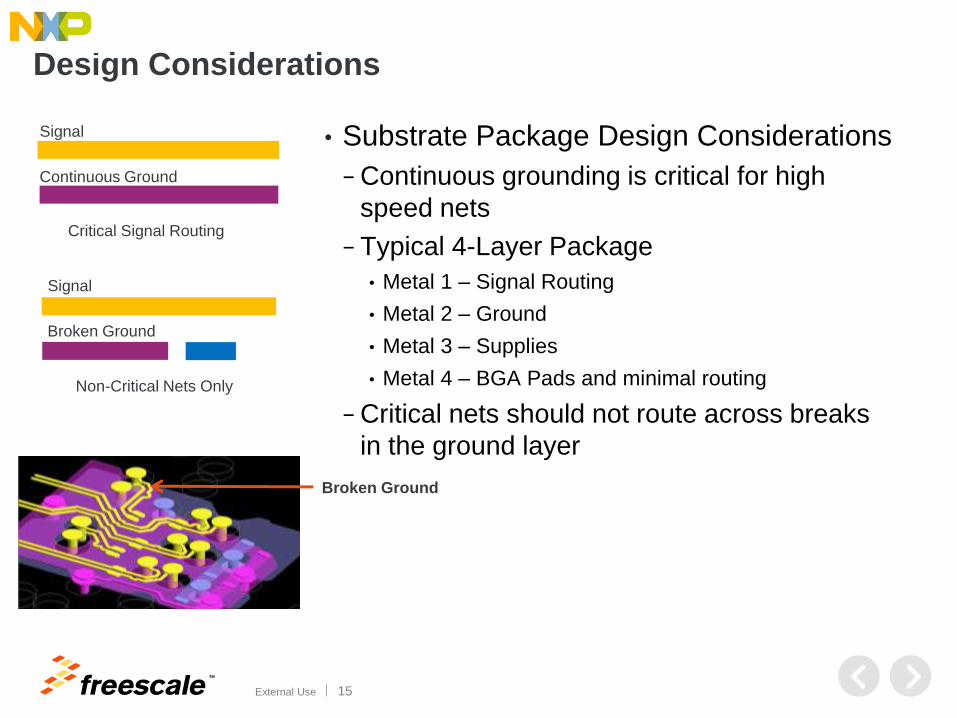
Design Considerations
• Substrate Package Design Considerations
− Continuous grounding is critical for high
speed nets
− Typical 4-Layer Package
• Metal 1 – Signal Routing
• Metal 2 – Ground
• Metal 3 – Supplies
• Metal 4 – BGA Pads and minimal routing
− Critical nets should not route across breaks
in the ground layer
Signal
Continuous Ground
Critical Signal Routing
Signal
Broken Ground
Non-Critical Nets Only
Broken Ground

TM
External Use 16
Optimizing Power Integrity
TM
External Use 17
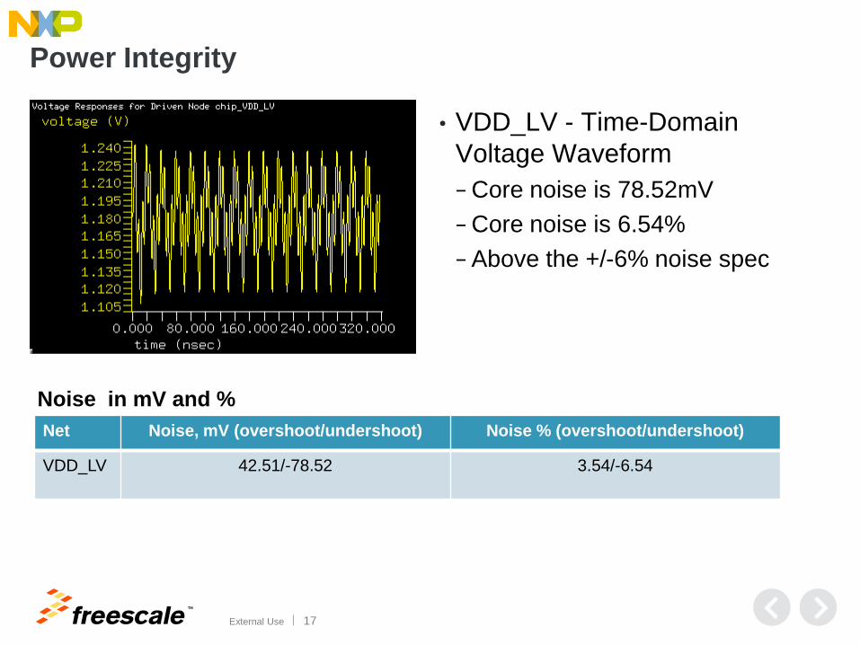
Power Integrity
• VDD_LV - Time-Domain
Voltage Waveform
− Core noise is 78.52mV
− Core noise is 6.54%
− Above the +/-6% noise spec
Noise in mV and %
Net Noise, mV (overshoot/undershoot) Noise % (overshoot/undershoot)
VDD_LV 42.51/-78.52
3.54/-6.54
TM
External Use 18
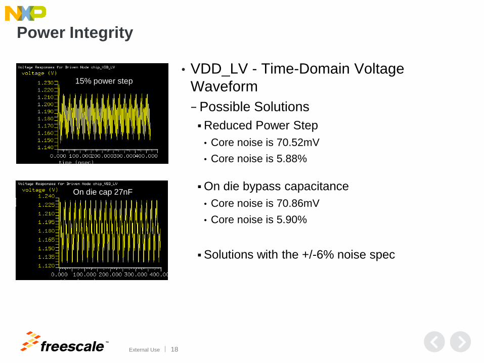
Power Integrity
• VDD_LV - Time-Domain Voltage
Waveform
− Possible Solutions
Reduced Power Step
• Core noise is 70.52mV
• Core noise is 5.88%
On die bypass capacitance
• Core noise is 70.86mV
• Core noise is 5.90%
Solutions with the +/-6% noise spec
15% power step
On die cap 27nF
TM
External Use 19
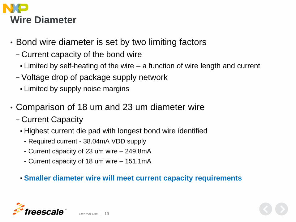
Wire Diameter
• Bond wire diameter is set by two limiting factors
− Current capacity of the bond wire
Limited by self-heating of the wire – a function of wire length and current
− Voltage drop of package supply network
Limited by supply noise margins
• Comparison of 18 um and 23 um diameter wire
− Current Capacity
Highest current die pad with longest bond wire identified
• Required current - 38.04mA VDD supply
• Current capacity of 23 um wire – 249.8mA
• Current capacity of 18 um wire – 151.1mA
Smaller diameter wire will meet current capacity requirements
TM
External Use 20
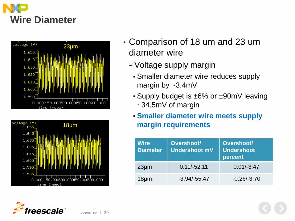
Wire Diameter
• Comparison of 18 um and 23 um
diameter wire
− Voltage supply margin
Smaller diameter wire reduces supply
margin by ~3.4mV
Supply budget is ±6% or ±90mV leaving
~34.5mV of margin
Smaller diameter wire meets supply
margin requirements
23μm
18μm
Wire
Diameter
Overshoot/
Undershoot mV
Overshoot/
Undershoot
percent
23μm 0.11/-52.11 0.01/-3.47
18μm -3.94/-55.47 -0.26/-3.70
TM
External Use 21
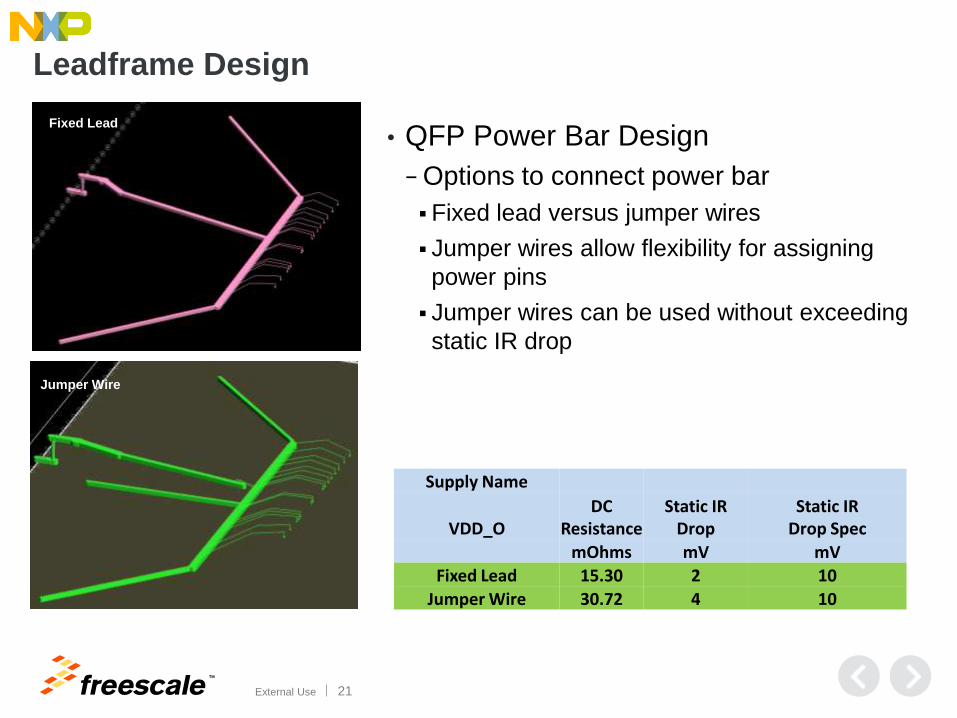
Leadframe Design
• QFP Power Bar Design
− Options to connect power bar
Fixed lead versus jumper wires
Jumper wires allow flexibility for assigning
power pins
Jumper wires can be used without exceeding
static IR drop
Supply Name
VDD_O DC
Resistance Static IR
Drop Static IR
Drop Spec
mOhms mV mV
Fixed Lead 15.30 2 10
Jumper Wire 30.72 4 10
Fixed Lead
Jumper Wire

TM
External Use 22
Maintaining Signal Integrity
TM
External Use 23
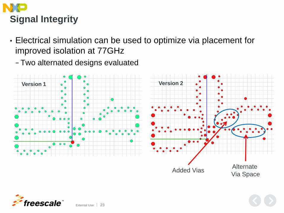
Signal Integrity
• Electrical simulation can be used to optimize via placement for
improved isolation at 77GHz
− Two alternated designs evaluated
Version 1 Version 2
Added Vias Alternate
Via Space
TM
External Use 24
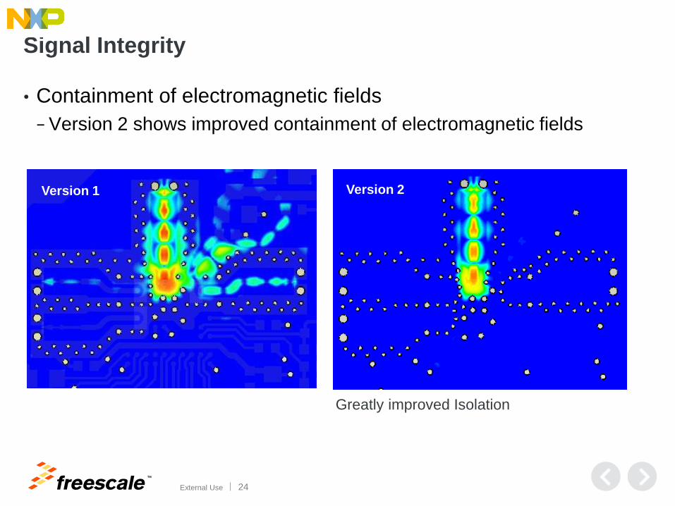
Signal Integrity
• Containment of electromagnetic fields
− Version 2 shows improved containment of electromagnetic fields
Version 1
Greatly improved Isolation
Version 2
TM
External Use 25
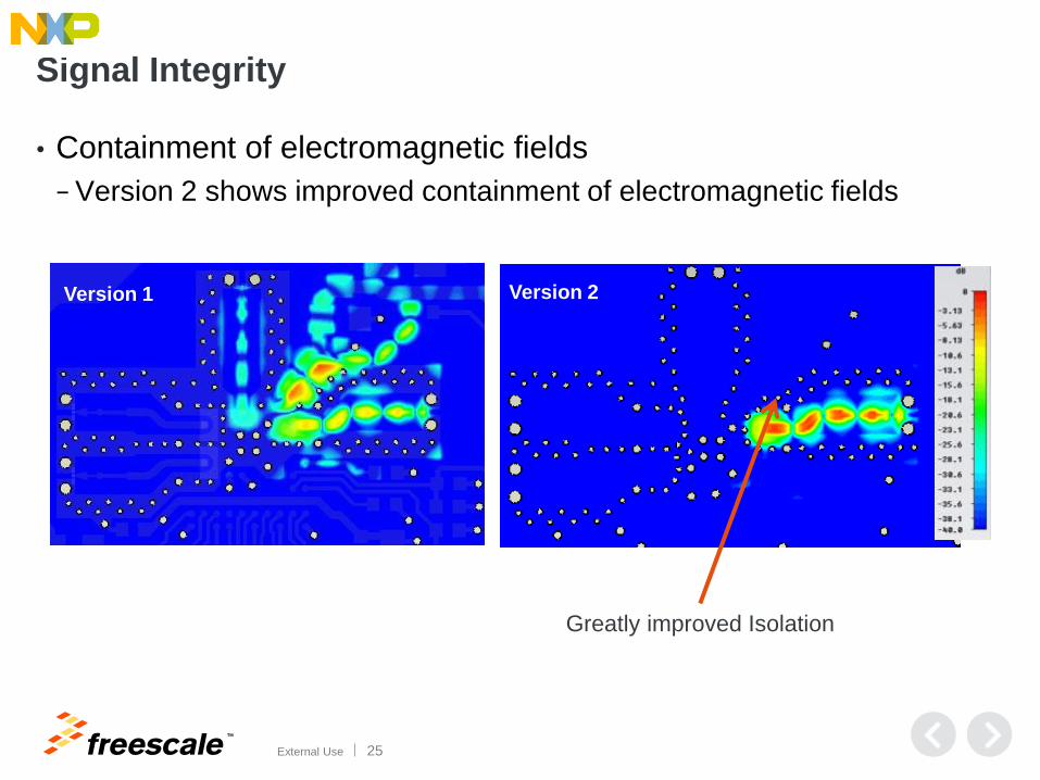
Signal Integrity
• Containment of electromagnetic fields
− Version 2 shows improved containment of electromagnetic fields
Version 1
Greatly improved Isolation
Version 2
TM
External Use 26
IBIS Models
TM
External Use 27
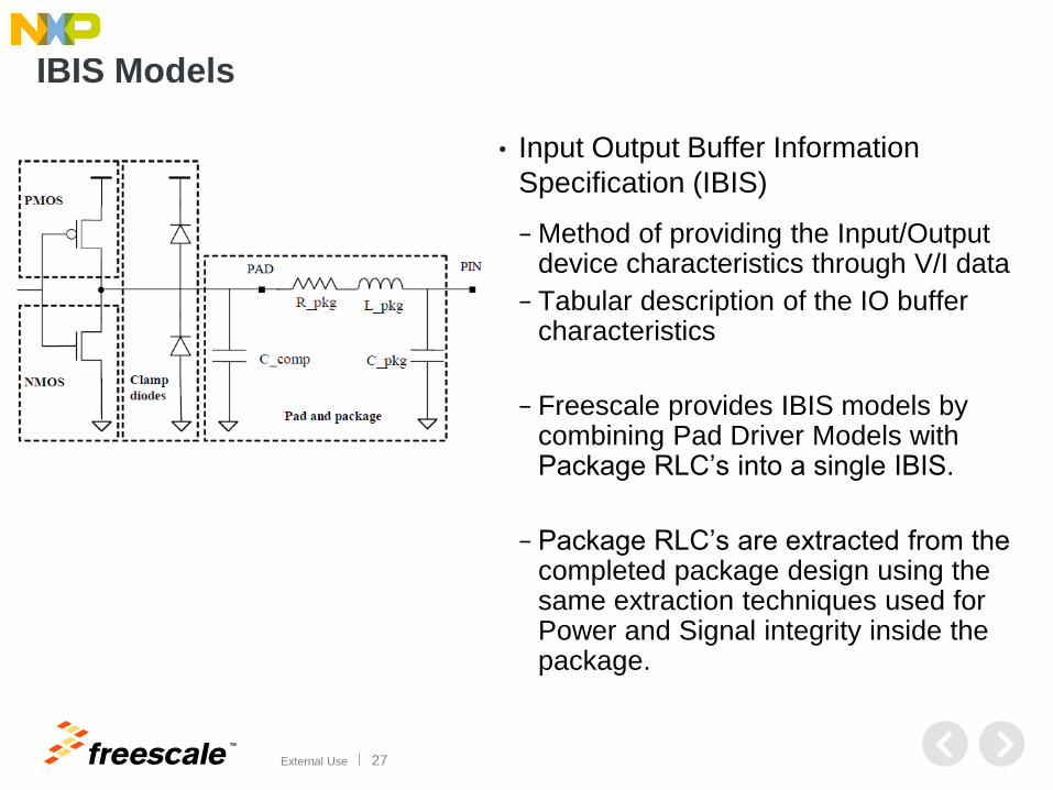
IBIS Models
• Input Output Buffer Information
Specification (IBIS)
− Method of providing the Input/Output device characteristics through V/I data
− Tabular description of the IO buffer characteristics
− Freescale provides IBIS models by combining Pad Driver Models with Package RLC’s into a single IBIS.
− Package RLC’s are extracted from the completed package design using the same extraction techniques used for Power and Signal integrity inside the package.
TM
External Use 28
Session Summary
• The integrated circuit package is a vital portion of overall system
performance
• A well designed package will
− Maintain power integrity
− Insure signal integrity
• IBIS models including package parasitics enable board and system
level simulation
TM
External Use 29
For Further Information
• IBIS Open Forum http://www.eda.org/ibis/
• Validating and Using IBIS files
http://www.national.com/appinfo/lvds/files/wp_ibis_validate.pdf
• Signal Integrity http://bethesignal.com
• My Contact information
− Neil Tracht – Manager of Package Design and Electrical Modeling
TM
External Use 30
Closing
• By now, you should be able to:
− Describe package parasitics
− Describe analysis techniques used to insure robust package
performance
− Describe package design considerations used to optimize package
performance
TM
© 2014 Freescale Semiconductor, Inc. | External Use
www.Freescale.com