Embed Size (px)
Citation preview
Simulation and Modeling of Silicon-Carbide
Devices
Simulation und Modellierung von
Siliziumkarbid-Bauelementen
der Technischen Fakultät
der Friedrich-Alexander-Universität
Erlangen-Nürnberg
zur Erlangung des Grades
Doktor-Ingenieur
vorgelegt von
Viktoryia Uhnevionak aus Genf
Als Dissertation genehmigt
von der Technischen Fakultät
der Friedrich-Alexander-Universität Erlangen-Nürnberg
Tag der mündlichen Prüfung: 10/03/2015
Vorsitzende des Promotionsorgans: Prof. Dr.-Ing. M. Merklein
Gutachter: PD Dr. Peter Pichler
Prof. Dr.-Ing. Robert Weigel
i
Abstract
In recent years, silicon carbide (SiC) became an attractive material and opened new perspectives
in power electronics due to its superior material properties. The wide bandgap, high thermal
conductivity and high breakdown electric field make SiC a material of choice for power
MOSFETs. The incorporation of SiC MOSFETs, for example, in power converters allows to
decrease their weight and size. This can be a big advantage for many applications including
electric cars. The ability of SiC devices to withstand high temperatures simplifies the thermal
management of the electrical systems. However, the commercial use of MOSFETs is currently
limited by technological problems which result in low channel mobility and high turn-on voltage.
The aim of this thesis was to understand and explain the mechanisms which control the channel
mobility in SiC MOSFETs using numerical simulation and to develop a self-consistent
simulation methodology for a description of their electrical behavior. For technological progress,
development and optimization of semiconductor devices, TCAD simulation became an
increasingly important tool of investigation. However, for SiC devices TCAD simulation
currently is a big challenge. Most of the simulation models were developed for silicon, and, thus,
can not adequately describe the transport properties of SiC devices. Moreover, because of a high
density of interface traps at the SiC/SiO2 interface, which strongly degrade the channel mobility
of SiC MOSFETs, an accurate interface trap model is of primary importance for the simulation.
In the framework of the MobiSiC (Mobility Engineering for SiC Devices) project lateral n-
channel 4H-SiC MOSFETs have been fabricated and electrically characterized by current-
voltage and Hall-effect measurements. The effects of temperature and bulk potential engineering
upon the transport properties in the channel of SiC MOSFETs have been studied. The
interpretation of the electrical measurements, i. e. current-voltage characteristics (ID(VG)) as well
ii
as sheet carrier density and channel mobility obtained from the Hall-effect measurements
(ninv(VG), 𝜇 (VG)), has been performed within this work using numerical simulation with
Sentaurus Device of Synopsys.
For an accurate evaluation of the Hall-effect measurements, a new method for the calculation of
Hall factors was developed. It is based on the fact that both Hall factor and mobility depend on
the same mechanisms by which the charge carriers are scattered. The method of calculation
accounts for all electron scattering mechanisms in the active area of the device. Thus, for the first
time, an accurate Hall factor has been calculated for the channel of MOSFETs and applied for
the correction of the Hall-effect measurements.
Experimental data, for example from Hall-effect measurements, is often used to characterize the
density of interface traps. In this work, a new method, which allows a more accurate
characterization, is suggested. In the first step, the densities of the interface traps versus trap
energy (DIT (ET)) are extracted from the Hall-effect and capacitance-voltage measurements using
a conventional method. Afterwards, the extracted DIT (ET) distributions are introduced into
Sentaurus Device and optimized numerically to minimize the deviations between the numerically
simulated characteristics (ninv(VG), 𝜇 (VG), and ID (VG)) and the experimentally measured data.
The numerical simulation allows to take into account, for instance, the effects of potential drop
along the channel between source and drain as well as the Fermi-Dirac distribution of the
electrons. These effects are neglected when the interface trap density is extracted conventionally
from the experimental data. Thus, it is expected that the new method produces physically more
reasonable results on the DIT (ET) distributions. Based on the experimental and simulated results,
origin and nature of the interface defects are discussed.
The simulation methodology, in which the method of the Hall factor calculation and the method
of the DIT (ET) extraction are accounted for, could consistently describe the temperature
dependence as well as the doping dependence of the transport properties of SiC MOSFETs
studied in this thesis. On the basis of a good agreement between simulations and measurements,
a comprehensive interpretation of the scattering mechanisms in the channel of SiC MOSFETs
with different doping concentrations and at different temperatures has been performed. One of
iii
the main findings from this work is that a decrease of the interface trap density is not the only
factor which can improve the performance of SiC MOSFETs. For example, their performance
can be improved significantly by decreasing the doping concentration of the channel. It was also
found that the doping concentration of the channel affects the temperature dependence of the
channel mobility: At elevated temperatures for highly doped MOSFETs it increases with
increasing temperature while for lowly doped ones it decreases.

v
Zusammenfassung
In den letzten Jahren wurde Siliziumkarbid (SiC) ein attraktives Material für die
Leistungselektronik und öffnete wegen seiner überlegenen Materialeigenschaften neue
Perspektiven auf diesem Gebiet. Der hohe Bandabstand, die hohe thermische Leitfähigkeit und
die hohe Durchbruchfeldstärke machen SiC zum Material der Wahl für Leistungs-MOSFETs.
Die Verwendung von SiC MOSFETs in Leistungswandlern erlaubt zum Beispiel eine
Verringerung deren Gewicht und Größe. Das kann ein großer Vorteil für viele Anwendungen
inklusive Elektroautos sein. Die Fähigkeit von SiC Bauelementen, auch bei hohen Temperaturen
zu funktionieren, vereinfacht das Wärmemanagement von elektrischen Systemen. Die
kommerzielle Nutzung von SiC MOSFETs ist derzeit jedoch durch technologische Probleme
begrenzt, die sich in Form von niedrigen Kanalbeweglichkeiten und hohen Einschaltspannungen
manifestieren.
Der Zweck dieser Doktorarbeit war, durch numerische Simulationen den Mechanismus zu
verstehen und zu erklären, der in SiC MOSFETs die Kanalbeweglichkeit bestimmt und eine
selbstkonsistente Simulationsmethodologie zur Beschreibung der elektrischen Eigenschaften von
SiC MOSFETs zu entwickeln. Für den technologischen Fortschritt, sowie für die Entwicklung
und Optimierung von Halbleiterbauelementen ist der rechnergestützte Entwurf von
elektronischen Bauelementen und ihrer Herstellung (TCAD – Technology Computer Aided
Design) zu einem zunehmend wichtigen Untersuchungswerkzeug geworden. TCAD-
Simulationen für SiC-Bauelemente sind aktuell jedoch eine große Herausforderung. Die meisten
Simulationsmodelle wurden für Silizium entwickelt und können deshalb die
Transporteigenschaften von SiC-Bauelementen nicht adäquat beschreiben. Darüber hinaus ist die
Grenzschicht zwischen Siliziumkarbid und Gateoxiden durch eine hohe Konzentration von

vi
Haftstellen charakterisiert, die die Kanalbeweglichkeit in SiC-MOSFETs stark degradieren.
Deshalb ist ein genaues Modell für die Haftstellen an der Grenzschicht von vorrangiger
Bedeutung für die Simulation.
Im Rahmen des Projekts MobiSiC (Mobility Engineering for SiC Devices) wurden laterale n-
Kanal 4H-SiC MOSFETs hergestellt und elektrisch durch Strom-Spannungs- und
Halleffektmessungen charakterisiert. Die Effekte von Temperatur und Substratdotierung auf die
Transporteigenschaften im Kanal von SiC MOSFETs wurden untersucht. Die Interpretation
sowohl der Strom-Spannungskennlinen (𝐼𝐷(𝑉𝐺)) als auch der aus den Halleffektmessungen abge-
leiteten Schichtladungsträgerkonzentrationen und Kanalbeweglichkeiten (𝑛𝑖𝑛𝑣(𝑉𝐺),𝜇(𝑉𝐺))wurden
in dieser Arbeit mit Hilfe numerischer Simulationen mit Sentaurus Device von Synopsys
durchgeführt.
Zur genauen Analyse der Halleffektmessungen wurde eine neue Methode der Berechnung des
Hallfaktors entwickelt. Sie beruht auf der Tatsache, dass sowohl der Hallfaktor als auch die
Beweglichkeit von denselben Mechanismen bestimmt werden, durch die die Ladungsträger
gestreut werden. Die Berechnungsmethode berücksichtigt alle Streumechanismen im aktiven
Bereich der Bauelemente. Auf diese Weise ist es zum ersten Mal möglich, einen genauen Wert
für den Hallfaktor für den Kanal von MOSFETs zu berechnen und für die Korrektur der
Halleffektmessungen zu verwenden.
Experimentelle Daten, z. B. von Halleffektmessungen, werden oft zur Charakterisierung der
Dichte von Haftstellen an der Grenzschicht verwendet. In dieser Arbeit wird eine neue Methode
vorgeschlagen, die eine genauere Charakterisierung erlaubt. In einem ersten Schritt werden
Haftstellendichten als Funktion der Energie (𝐷𝐼𝑇(𝐸𝑇)) von Halleffekt- und Kapazitäts-
Spannungsmessungen auf konventionelle Art extrahiert. Danach werden sie in Sentaurus Device
eingegeben und numerisch optimiert um die Abweichungen zwischen den simulierten
Kennlinien (𝐼𝐷(𝑉𝐺), 𝑛𝑖𝑛𝑣(𝑉𝐺) und 𝜇(𝑉𝐺)) und den Messungen zu minimieren. Die numerische
Simulation erlaubt, Effekte wie z.B. die Potentialverteilung zwischen Source und Drain sowie
die Fermi-Dirac-Verteilung der Elektronen zu berücksichtigen. Solche Effekte bleiben bei der
konventionellen Extraktion der Haftstellendichte unberücksichtigt. Es ist deshalb zu erwarten,
vii
dass die neue Methode physikalisch schlüssigere Ergebnisse für Haftstellendichte 𝐷𝐼𝑇(𝐸𝑇)
liefert. Basierend auf den experimentellen Ergebnissen und den Simulationen werden Ursprung
und Natur der Grenzflächenhaftstellen diskutiert.
Die Simulationsmethodologie, in die die Methode der Berechnung von Hallfaktoren und die
Methode der Extraktion der Haftstellendichte eingingen, konnte konsistent die
Temperaturabhängigkeit sowie die Konzentrationsabhängigkeit der Transporteigenschaften der
in dieser Arbeit betrachteten SiC MOSFETs beschreiben. Auf der Basis der guten
Übereinstimmung zwischen Simulationen und Messungen konnten die Streumechanismen im
Kanal von SiC MOSFETs mit unterschiedlichen Dotieratomkonzentrationen und bei
unterschiedlichen Temperaturen umfassend interpretiert werden. Eine der Haupterkenntnisse
dieser Arbeit ist, dass eine Verringerung der Grenzflächenhaftstellendichte nicht der einzige
Faktor zur Verbesserung der Eigenschaften von SiC MOSFETs ist. Ihre Eigenschaften können
z.B. auch durch eine Verringerung der Kanaldotierung erheblich verbessert werden. Weiterhin
wurde gefunden, dass die Konzentration der Kanaldotierung die Temperaturabhängigkeit der
Kanalbeweglichkeit beeinflusst: Bei hochdotierten MOSFETs steigt sie mit der Temperatur
während sie sich bei niedrig dotierten MOSFETs verringert.

ix
Contents
Abstract…….. .................................................................................................................................. i
Zusammenfassung........................................................................................................................... v
Chapter 1 Introduction ............................................................................................................... 1
1.1 SiC as a wide bandgap semiconductor ............................................................................. 1
1.2 TCAD for the development and optimization of semiconductor devices ........................ 4
1.3 Lateral 4H-SiC MOSFETs: Literature review ................................................................. 6
1.4 Thesis outline ................................................................................................................... 8
Chapter 2 Simulation and Experimental Setup........................................................................ 11
2.1 Basic concept of a device simulation ............................................................................. 11
2.2 Description of the MOSFET structures and fabrication processes ................................ 13
2.3 Description of electrical measurements of SiC MOSFETs ............................................ 15
Chapter 3 Physical Models ...................................................................................................... 17
3.1 Fermi-Dirac statistics ..................................................................................................... 17
3.2 Bandgap energy and its temperature dependence .......................................................... 19
x
3.3 Incomplete ionization ..................................................................................................... 21
3.4 Near-Interface Trap model ............................................................................................. 26
3.4.1 The fundamental knowledge of traps ...................................................................... 26
3.4.2 Simulation of the interface trap density in n-channel SiC MOSFETs .................... 31
3.5 Mobility degradation model ........................................................................................... 36
Chapter 4 Extraction of the Density of Interface Traps from Electrical Measurements ......... 41
4.1 Hall-effect measurements ............................................................................................... 41
4.2 Capacitance-voltage measurements: High-low frequency method ................................ 47
Chapter 5 Method of Hall Factor Calculation ......................................................................... 55
5.1 On the calculation of Hall factor for the characterization of electronic devices ............ 56
5.2 Hall factor in bulk silicon ............................................................................................... 60
Chapter 6 Simulation Results and Discussions ....................................................................... 65
6.1 Simulation methodology: Current-voltage characteristics ............................................. 65
6.2 Simulation methodology: Hall-effect measurements ..................................................... 75
6.3 Effect of bulk potential engineering upon transport properties in SiC MOSFETs ........ 84
6.4 On the temperature dependence of the electrical characteristics of SiC MOSFETs ...... 99
Chapter 7 Conclusions and Outlook ...................................................................................... 113
Acknowledgement ...................................................................................................................... 117
References…. .......................................................................................................................... …119
xi
Thesis Publications ..................................................................................................................... 131
List of Figures ............................................................................................................................. 133
List of Tables .............................................................................................................................. 139
List of Symbols ........................................................................................................................... 141
Index………... ............................................................................................................................ 145

1
Chapter 1 Introduction
1.1 SiC as a wide bandgap semiconductor
Today, silicon (Si) is the basic material for the manufacturing of most power semiconductor
devices. In many fields of application, however, Si-based power electronics has already reached
its theoretical limit. An increase of the need of electric power as well as the rising costs of energy
makes silicon less competitive for many applications. An efficient energy management becomes
one of the utmost challenges at the present time. One of the solutions to meet high power
requirements is to replace silicon by wide-bandgap (WBG) semiconductors, e.g. silicon carbide
(SiC), gallium nitride (GaN), a diamond, the properties of which are very exciting [1]:
Firstly, the use of WBG semiconductors for the electronic devices has the advantage for high-
temperature operation where an uncontrolled conduction of electrons is prevented due to the
higher thermal energy needed for electrons to move from the valence band to the conduction.
Secondly, WBG semiconductors have a large electric breakdown field which results in higher
breakdown voltages (VBR) for power devices and allows usage of much higher doping levels for
the same VBR in comparison with Si. As a result, WBG-semiconductor-based power devices have
lower on-resistances of the drift region.
Thirdly, the electron saturation velocities of the WBG semiconductors are higher than in Si.
Considering that saturation velocity is directly proportional to the high-frequency switching
capability of a semiconductor, WBG semiconductor-based power devices could be switched at
higher frequencies than Si-based ones.
2 Chapter 1 Introduction
Fourthly, SiC and diamond have higher thermal conductivities in comparison with Si. This
property allows material to dissipate the heat of the device to its surroundings better, resulting in
lower increase of the device temperature. As a conclusion, due to the wide bandgap, devices built
with WBG materials can operate at higher temperatures, higher voltages and higher frequencies.
These abilities make them interesting for use in future electronic systems under conditions where
Si-based devices cannot be used.
One of the WBG candidates for the replacement of Si, which is widely investigated now, is SiC.
Due to its unique physical and electronic properties it shows a great promise for the future of
power electronics. SiC has a huge amount of different polytypes, however, 4H-SiC is often
chosen as the most suitable for the power electronics due to its wider bandgap and higher bulk
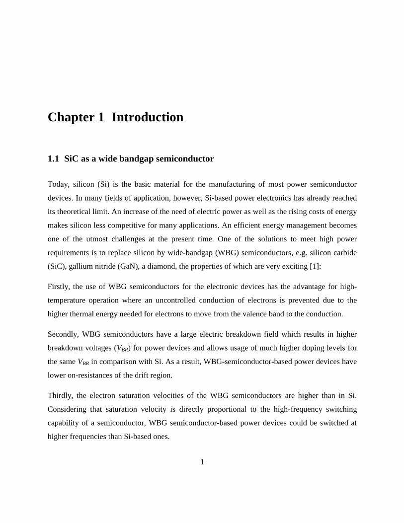
mobility. Table 1 compares the most important material properties of Si and 4H-SiC.
Table 1. Material properties of 4H-SiC and Si [1]
Material Property Si 4H-SiC
Bandgap (eV) 1.12 3.26
Electric breakdown field (106 V/cm) 0.3 2.2
Electron mobility (cm2/Vs) 1500 1000
Electron saturation velocity (107 cm/s) 1 2
Thermal conductivity (W/K·cm) 1.5 4.9
From Table 1 it is obvious that for power electronics 4H-SiC surpasses Si: Three times larger
bandgap, nearly ten times higher electric breakdown field and more than three times higher
thermal conductivity. In comparison with other WBG semiconductors with similar material
properties, SiC has a significant advantage. This advantage is related to the ability to form SiO2
layers on SiC by thermal oxidation in a way similar to Si, providing a good basis for the
fabrication of MOS-based electronic devices. However, the opportunity to have SiO2 as its native
oxide can be considered nowadays not only as a great advantage but at the same time as a critical
factor for the electrical applications. The high density of imperfections encountered in thermally
grown oxide as well as at the SiC/SiO2 interface represents a major obstacle for the performance
1.1 SiC as a wide bandgap semiconductor 3
of SiC MOS-devices [2]. For power MOSFETs, where one of the main requirements is a low
power loss at on-state, and, thus, a low on-resistance, the quality of the SiC/SiO2 interface is of
primary importance. For example, for Vertical Diffused MOS, where the on-resistance of the
drift region is low because of the high electric breakdown field of SiC, the overall performance
of the device diminishes because of the high on-resistance of the channel at the interface. Thus,
to use the full potential of SiC for the development of power electronics, the quality of the
SiC/SiO2 interfaces has to be improved [3].
To understand better the mechanisms which control the mobility in the channel at the interface
and, thus, to improve channel mobility, lateral SiC MOSFETs are widely used for investigations.
The very low channel mobility and the corresponding low channel current are the biggest issues
for lateral SiC MOSFETs. Their low performance is usually related to the presence of a large
number of interface defects at the SiC/SiO2 interface. Despite that the oxide appears to be similar
to that grown on silicon, the oxidation process in the presence of carbon is different and leads to
a higher defect density at the interface. For clarity, the density of interface traps at the Si/SiO2
interface in modern CMOS technology does not exceed 1010
cm-2
eV-1
. In contrast, at the
SiC/SiO2 interface, this value is about ~1011
cm-2
eV-1
in the middle of the bandgap and
~1013
cm-2
eV-1
or even more at the band edges in 4H-SiC [4]. The question how to reduce these
defects at the SiC/SiO2 interface has become a key issue in the development of SiC MOS
technology.
The standard method to reduce the interface defects by passivation with hydrogen known from Si
MOS processing is not sufficient for the SiC/SiO2 structures. This leads to the necessity to
improve the processing technology and make additional material research. Currently, one of the
most used methods for the improvement of SiC/SiO2 interfaces is nitridation [5]. It has been
found that the alternative method through oxidation and post-annealing in a nitrogen-containing
atmosphere can reduce the interface defects by as much as a factor of ~ 2-4 [6,7]. However, the
amount of traps at the SiC/SiO2 interface still surpasses the amount of traps at the Si/SiO2
interface resulting in a limitation of the commercial use of SiC MOS-based devices. Thus, to
4 Chapter 1 Introduction
understand better the nature of defects, to find technologically feasible methods to eliminate
them and to improve the channel mobility of MOSFETs are the main tasks for the future research
of SiC MOS technology. On the current stage of SiC research, simulation is an important
instrument of the investigations. For example, simulation of processes and devices helps to
understand better effects which can have an impact upon the performance of SiC devices and,
thus, to find faster the solution needed to achieve a progress in the SiC device development.
1.2 TCAD for the development and optimization of semiconductor devices
During the last decades the software for the Technology Computed Aided Design (TCAD) has
been strongly improved with the purpose to support the development and optimization of
semiconductor technologies, devices and circuits. The market for TCAD tools is currently
dominated by the company Synopsys [8] which offers a variety of integrated tools for IC design.
Device simulation and model development is only one of its components which allows to
visualize device behavior. Considering that computer resources started to be much cheaper in
comparison with costs of experimental investigations, device modeling and simulation became a
more and more important tool in research environments as well as in industry [9].
One of the most important advantages of using TCAD simulation and modeling is to allow deep
insight and understanding of physical processes involved in the device operation. In addition, the
estimation of the International Technology Roadmap for Semiconductor (ITRS) shows that the
use of TCAD can help to reduce the cost and time required for the device development by up to
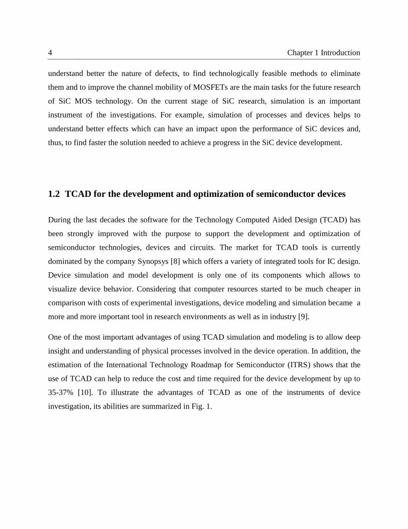
35-37% [10]. To illustrate the advantages of TCAD as one of the instruments of device
investigation, its abilities are summarized in Fig. 1.
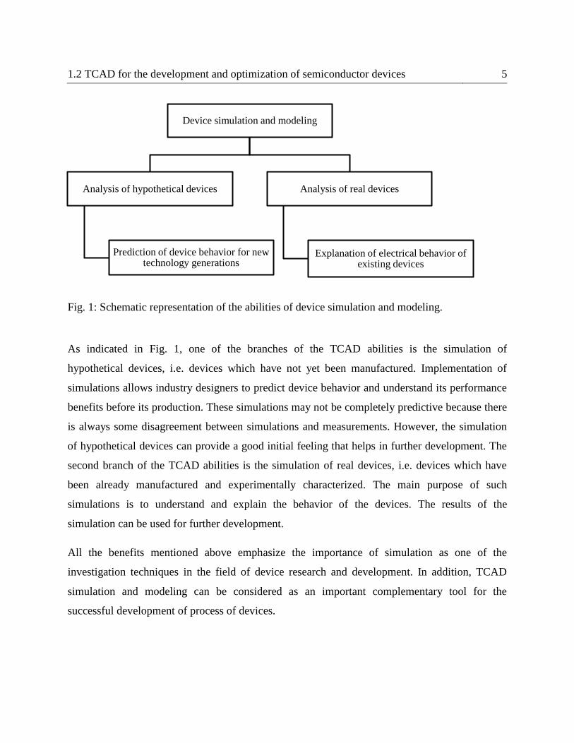
1.2 TCAD for the development and optimization of semiconductor devices 5
Fig. 1: Schematic representation of the abilities of device simulation and modeling.
As indicated in Fig. 1, one of the branches of the TCAD abilities is the simulation of
hypothetical devices, i.e. devices which have not yet been manufactured. Implementation of
simulations allows industry designers to predict device behavior and understand its performance
benefits before its production. These simulations may not be completely predictive because there
is always some disagreement between simulations and measurements. However, the simulation
of hypothetical devices can provide a good initial feeling that helps in further development. The
second branch of the TCAD abilities is the simulation of real devices, i.e. devices which have
been already manufactured and experimentally characterized. The main purpose of such
simulations is to understand and explain the behavior of the devices. The results of the
simulation can be used for further development.
All the benefits mentioned above emphasize the importance of simulation as one of the
investigation techniques in the field of device research and development. In addition, TCAD
simulation and modeling can be considered as an important complementary tool for the
successful development of process of devices.
Device simulation and modeling
Analysis of hypothetical devices
Prediction of device behavior for new technology generations
Analysis of real devices
Explanation of electrical behavior of existing devices

6 Chapter 1 Introduction
For SiC devices TCAD simulation currently is a big challenge. Most of the models were
developed for silicon, and, thus, can not adequately describe transport properties of SiC devices.
To use simulation to explain the behavior of SiC devices, numerical models have to be
calibrated.
1.3 Lateral 4H-SiC MOSFETs: Literature review
The commercialization of n-channel lateral SiC MOSFETs is still limited due to their low
electrical performance which is related to the high amount of defects at the SiC/SiO2 interface.
According to literature, there are two main classes of defects which contribute to the distribution
of the interface trap density of states (DIT (ET)) across the SiC bandgap [11]: A first class of
defects covers the entire SiC bandgap with a density not exceeding 1012
cm-2
eV-1
. A second class
of defects, known as near-interface traps (NITs), consists of electron traps near the SiC
conduction band. The peak density of NITs reaches 1013
cm-2
eV-1
and sometimes 1014
cm-2
eV-1
.
Furthermore, the total DIT distribution in the bandgap is not uniform over energy; by spreading
across the SiC bandgap it forms four broad peaks [12]. Different theoretical and experimental
studies have been performed to find out the origin of these defects and understand the difference
in their densities compared with the defects at the Si/SiO2 interface.
In one of the publications of Afanas’ev [13], to explain the defect density at the SiC/SiO2
interface, it was suggested to consider the following aspects:
a higher surface density of atoms per unit area in SiC than in Si which may lead to a
higher density of dangling bonds at the interface (e.g., on 4H-SiC (0001), the surface
density is 1.21·1015
at/cm2, on Si (100) – 6.8·10
14 at/cm
2);
a larger width of the 4H-SiC bandgap energy in comparison with Si which may allow the
oxide defects located near the interface to appear in the SiC bandgap and behave like
interface traps;
1.3 Lateral 4H-SiC MOSFETs: Literature review 7
the presence of the carbon which may involve additional chemical complexity of the SiC
oxidation and potentially leads to a specific defect generation in SiO2.
The question of the origin of defects at the SiC/SiO2 interface is quit complicated and remains so
far not well understood. Using photon stimulated tunneling (PST) measurements on SiC and Si-
based MOS structures, traps with an energy level 2.8 eV below the conduction band of SiO2 have
been found in comparable densities in both oxides grown on Si and SiC [14,15]. In the 4H-SiC
bandgap, these traps are positioned 0.1 eV below the conduction band, which corresponds to the
energetic location of NITs. Based on that and considering the universality of the defects in SiO2
layers grown on SiC and Si, it was suggested to relate NITs to oxide defects introduced during
the oxidation process. From the theoretical investigations, it was also concluded that NITs
originate from oxide defects near the interface. In addition, it was mentioned that one part of the
NITs can be related to defects specific to SiO2 on SiC formed in the oxide phase [16]. The
interface traps in the lower part of the bandgap are explained mainly by carbon-related structures
at the interface [4,16,17].
The presence of a large amount of traps at the SiC/SiO2 interface leads to a degradation of the
mobility in the channel of SiC MOSFETs. Typical values of the field-effect electron mobility in
lateral 4H-SiC MOSFETs with oxides grown by dry O2 oxidation are less than 10 cm2/Vs. To
improve such a low channel mobility, different techniques for the reduction of the density of
interface traps were introduced. One of it is the use of hydrogen annealing as a precleaning stage
for gate oxidation. By this technique, Ueno et al. obtained a field-effect mobility of 20 cm2/Vs
for MOSFETs with a p-type channel doping of 3·1016
cm-3
[18]. Another method, which is the
most common one nowadays, is the oxidation or post-oxidation annealing in NO or N2O
ambients [5,19]. As an example, Fujihira et al. got a field-effect mobility of 30 cm2/Vs for a
MOSFETs with p-type doping of 1·1016
cm-3
[20]. As an alternative technique, it was shown that
phosphorus passivation decreases the interface trap density even more and increases mobility by
a factor of 2 in comparison to the standard nitridation [21]. By POCl3 annealing Okamoto
improved the channel mobility and obtained a peak field-effect mobility of 89 cm2/Vs for a
8 Chapter 1 Introduction
channel doping concentration of 7·1015
cm-3
[22]. Another oxidation method which is more
efficient in the reduction of the interface traps is the sodium-enhanced oxidation [23,24].
However, this method has a big disadvantage. Due to the presence of sodium (Na) during the
oxidation process, mobile Na ions in the oxide are involved and may cause threshold voltage
instabilities.
As alternative method to oxidation techniques, nitrogen implantation in the channel region is
widely investigated to increase the channel mobility [25,26,27]. In the work of Strenger et al. the
effect of nitrogen implantation into the MOSFET channel region prior to oxidation in N2O
atmosphere was investigated [28]. For a p-doped substrate with a concentration of 3.5·1017
cm-3
the peak of the field-effect mobility after N2O oxidation was 12 cm2/Vs. Using implantation of
nitrogen with different doses for a MOSFETs with the same p-type doping concentration, an
increase in the field-effect mobility was observed. For nitrogen (N) doses of 1·1013
cm-2
,
3·1013
cm-2
and 5·1013
cm-2
, the peak of the field-effect mobility was equal to 17 cm2/Vs,
21 cm2/Vs and 25 cm
2/Vs, respectively.
As it can be seen from this short overview, many studies have been performed already to
understand and solve the problem of the low channel mobility by improving the SiC/SiO2
interface. However, there are still many unknown aspects and despite the enhancements which
have been already achieved, the channel mobility in 4H-SiC MOSFETs is still far from the
channel mobility in Si MOSFETs [29].
1.4 Thesis outline
This thesis presents a study of lateral n-channel 4H-SiC MOSFETs. The fabrication and
electrical characterization of all studied structures have been carried out in the framework of the
French-German cooperation project MobiSiC (Mobility engineering for SiC devices). The
fabrication of the devices, except MOSFETs #E1, has been done by C. Strenger at the
Fraunhofer IISB, Germany. The MOSFETs #E1 have been fabricated by Robert Bosch GmbH.
1.4 Thesis outline 9
The electrical characterization of all devices has been performed by E. Bedel-Pereira and V.
Mortet at LAAS-CNRS, France. A description of the studied MOSFET structures, their
fabrication processes and the experiments performed for their characterization are presented in
Chapter 2.
The main aim of this work was to understand the mechanisms which control the channel
mobility of SiC MOSFETs using TCAD simulation. For this purpose, current-voltage and Hall-
effect measurements have been interpreted in this thesis by two-dimensional numerical
simulations performed with Sentaurus Device of Synopsys.
To describe the electrical measurements of MOSFETs, a simulation methodology has been
developed and the following physical models with proper parameters for 4H-SiC were
introduced in the simulation:
Fermi-Dirac statistics
Bandgap energy model
Incomplete ionization model
Near-Interface Trap model
Mobility degradation model
A full description of the models with the parameters used will be given in Chapter 3.
For the characterization of the interface defects, the most crucial parameter for SiC MOSFETs,
their densities versus trap energies have been extracted from the electrical measurements. The
methods of the extraction of the DIT (ET) distributions are described in Chapter 4.
To interpret accurately channel mobilities obtained from Hall-effect measurements, the Hall
factor has been evaluated, for the first time, for the channel of SiC MOSFETs. The method
developed in this work for the calculation of the Hall factor is presented in Chapter 5.
The results of the simulations in comparison with the electrical measurements are shown and
discussed in Chapter 6. Therein, the simulation methodology developed to interpret the electrical

10 Chapter 1 Introduction
characteristics of MOSFETs will be presented. In addition, the effects of temperature and bulk
potential engineering upon the transport properties in the channel of SiC MOSFETs will be
discussed.
In Chapter 7 the main conclusions and an outlook will be given.
11
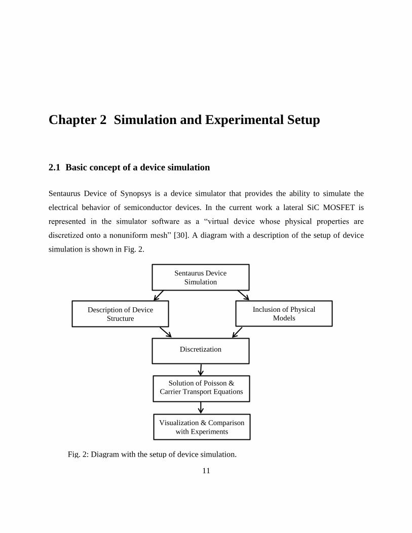
Chapter 2 Simulation and Experimental Setup
2.1 Basic concept of a device simulation
Sentaurus Device of Synopsys is a device simulator that provides the ability to simulate the
electrical behavior of semiconductor devices. In the current work a lateral SiC MOSFET is
represented in the simulator software as a “virtual device whose physical properties are
discretized onto a nonuniform mesh” [30]. A diagram with a description of the setup of device
simulation is shown in Fig. 2.
Fig. 2: Diagram with the setup of device simulation.
Solution of Poisson &
Carrier Transport Equations
Sentaurus Device
Simulation
Description of Device
Structure
Inclusion of Physical
Models
Discretization
Visualization & Comparison
with Experiments
12 Chapter 2 Simulation and Experimental Setup
As it can be seen in Fig. 2, the implementation of a simulation with Sentaurus Device starts with
the design of the device structure. Such information as device dimensions, material of the device
regions, location of electrical contacts and doping distributions have to be properly described in
the simulator. To achieve accurate simulation of real MOSFETs, in addition to the description of
the device structure, it is very important to define appropriate physical models in the simulation.
After defining the device structure and the physical models, simulation continues with solving
the equations that describe the carrier transport in the active region of the device. The equations
to be solved are
the Poisson equation,
∇ · (휀𝑆∇𝜓) = −𝑞(𝑝 − 𝑛 + 𝑁𝐷+ − 𝑁𝐴
−) − 𝜌𝑡𝑟𝑎𝑝 (1)
the electron and hole continuity equations,
𝜕𝑛
𝜕𝑡= 1
𝑞∇ · 𝐽𝑛 − 𝑅𝑛𝑒𝑡
(2)
𝜕𝑝
𝜕𝑡= −
1
𝑞∇ · 𝐽𝒑 − 𝑅𝑛𝑒𝑡
(3)
and the electron and hole current density equations
𝐽𝑛 = 𝑞𝜇𝑛𝑛ℰ + 𝑞𝐷𝑛∇𝑛 (4)
𝐽𝑝 = 𝑞𝜇𝑝𝑝ℰ − 𝑞𝐷𝑝∇𝑝 (5)
Therein, εS is the dielectric constant of the semiconductor, 𝜓 the electrostatic potential, q the
elementary charge, n and p are the electron and hole concentrations, 𝑁𝐷+ and 𝑁𝐴
− the
concentrations of ionized donor and acceptor impurities, 𝜌𝑡𝑟𝑎𝑝 is the surface charge density
which may be present due to the interface trap charges, Jn and Jp are the electron and hole current
densities, Rnet is the net recombination rate, Ɛ is the electric field, 𝜇n and 𝜇p are the electron and
2.2 Description of the MOSFET structures and fabrication processes 13
hole mobilities, and Dn and Dp the electron and hole diffusion coefficients. The diffusion
coefficients are related to the mobilities by the Einstein relations
𝐷𝑛 = 𝜇𝑛𝑘𝐵𝑇
𝑞
(6)
𝐷𝑝 = 𝜇𝑝𝑘𝐵𝑇
𝑞
(7)
where 𝑘𝐵 is Boltzmann’s constant and T is absolute temperature.
To obtain a numerical solution of the aforementioned equations, Sentaurus Device solves the
equations on a discrete mesh using Newton’s iterative method. After a numerical solution of the
equations is found, the simulated electrical characteristics can be visualized and compared with
experiments. The ability to compare simulations with experiments allows to check the accuracy
of the simulation results.
2.2 Description of the MOSFET structures and fabrication processes
To fabricate SiC n-channel lateral MOSFETs, several device manufacturing runs were
performed. In a first run, SiC MOSFETs (#E1) were manufactured on p-type 4° off-axis (0001)
Si-face 4H-SiC epitaxial layers with a thickness of 10 𝜇m and with an aluminum (Al)
concentration of 5∙1017
cm-3
. The gate oxide was grown by thermal oxidation in N2O atmosphere
at 1550 K for 180 min and annealed at the same temperature for 30 min in an N2 ambient. The
thickness of the gate oxide of the MOSFETs (#E1) is 34 nm. In a second run, SiC MOSFETs
(#E2, #W1, #W2) were fabricated on p-type 4° off-axis (0001) Si-face 4H-SiC epitaxial layer
with a thickness of 5 𝜇m and with different doping concentrations of Al. The Al concentrations
are 1∙1015
cm-3
, 1∙1016
cm-3
and 5∙1016
cm-3
for the samples #E2, #W1 and #W2, respectively. To
14 Chapter 2 Simulation and Experimental Setup
obtain Al concentrations of 1∙1016
cm-3
and 5∙1016
cm-3
, box-shaped, p-type wells were fabricated
by multiple Al-implantations into the epitaxial layer with a concentration of 1·1015
cm-3
. The
oxidation process was performed under the same conditions as in the first run but with a thermal
oxidation time of 150 min. Due to the shorter thermal oxidation, the oxide thickness of the
samples #E2, #W1, #W2 is 25.5 nm. The information about doping concentrations and gate
oxide thicknesses for all investigated MOSFETs is summarized in Table 2.
Table 2. Doping concentrations and oxide thicknesses for the investigated MOSFETs
Sample Doping concentration
epitaxial layer (cm-3
)
Doping concentration
p-type well (cm-3
)
Gate oxide thickness
(nm)
#E1 NA = 5∙1017
– 34
#E2 NA= 1∙1015
– 25.5
#W1 NA = 1∙1015
NA = 1∙1016
25.5
#W2 NA = 1∙1015
NA = 5∙1016
25.5
To form the gate electrode in both runs, phosphorus-doped polycrystalline silicon was deposited
and patterned. Source and drain regions were box implanted with nitrogen with a peak
concentration of 5∙1019
cm-3
. Afterwards, they were annealed in argon (Ar) at a temperature of
1970 K for 30 min. For the fabrication of the source, drain, bulk and p-well contacts, SiC was
alloyed with nickel (Ni) at 1370 K for 2 min and thereafter a metallization stack containing
titanium (Ti) and platinum (Pt) was deposited and patterned. The length (L) and width (W) of the
channel were 500 µm and 80 µm, respectively. It should be noted that all the investigated
MOSFETs are Hall-Bar structures which are designed with additional contact taps to the channel
region. A top view of the Hall-Bar structure is shown in Fig. 3. Further details of the fabrication
processes can be found in the work of C. Strenger [31].

2.3 Description of electrical measurements of SiC MOSFETs 15
Fig. 3: Top view of the Hall-Bar structure [31].
2.3 Description of electrical measurements of SiC MOSFETs
The MOSFETs studied in this work have been characterized electrically by current-voltage and
Hall-effect measurements at LAAS-CNRS, France. The drain-source voltage VD in the
measurements was set to 0.1 V and the gate voltage was varied from 0 V to 20 V. The Hall-
effect measurements were carried out using a permanent magnet with a magnetic field of 0.33 T.
Further details of the experiments and their setup can be found elsewhere [31].
From the results of the Hall-effect measurements the sheet carrier density of electrons ninv and
the drift mobility µ in the inversion layer were determined as a function of gate voltage from the
measurable quantities considering the Hall factor rH by the formulas:
𝑛𝑖𝑛𝑣 = 𝑟𝐻𝐼𝐷𝐵
𝑞𝑉𝐻
(8)
𝜇 = 1
𝑟𝐻
𝑉𝐻𝜌𝐼𝐷𝐵
(9)

16 Chapter 2 Simulation and Experimental Setup
Therein, ID denotes the channel current, B the magnetic field, VH the Hall-effect voltage, and ρ
the channel resistivity.
The electrical characterization of the MOSFETs has been carried out in the temperature range
from 50 K till 500 K. However, because of a bad convergence in the simulation at low
temperatures and, considering the importance of the application of SiC MOSFETs at high
temperatures, numerical simulations have been performed only from 300 K till 500 K. The
results of the electrical measurements interpreted in this work will be shown and discussed
together with the simulation results in Chapter 6.
17
Chapter 3 Physical Models
Device simulation depends significantly on the physical models and their parameters. However,
most of the programs for the simulation of the device characteristics are based on models
developed for silicon. Considering the difference between Si and SiC, parameter sets in the
physical models need to be adjusted for simulations of SiC devices.
In addition, for SiC MOS-device simulation, where one of the most crucial physical parameters
is the charge at the SiC/SiO2 interface, such models as Near-Interface Trap (NIT) and Mobility
degradation at the interface have to be properly included. The following sub-sections describe
the models and parameters used in the current work for 4H-SiC MOSFETs simulations.
3.1 Fermi-Dirac statistics
The fundamental understanding of the semiconductor devices is based on band structure of
semiconductors. In Sentaurus Device the energy band model is simplified by default and
characterized by four quantities [30]:
bandgap and electron affinity;
effective density of states for electrons and holes.
In reality the band structure of semiconductors is very complex and consists of a large number of
discrete energy states. These energy states form energy bands which are separated by gaps.
However, for the current flow in semiconductors only the valence and conduction bands are
important [32]. This is the reason for the simplification of the band structure used in device
simulation.
18 Chapter 3 Physical Models
The electron current in semiconductors is proportional to the free electrons in the conduction
band. The presence of electrons in the conduction band physically indicates that energetic states
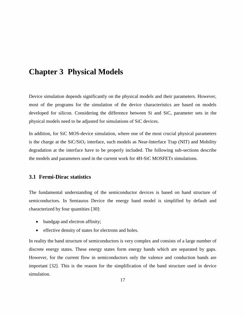
in the conduction band are occupied by electrons. To describe the free electron concentration, the
probability f (E) that an electron occupies an energy level E can be given by the Fermi-Dirac
statistic
𝑓(𝐸) =1
1 + 𝑒(𝐸−𝐸𝐹) 𝑘𝐵𝑇⁄
(10)
where EF is the Fermi level. The schematic representation of the Fermi-Dirac distribution is
shown in Fig. 4.
Fig. 4: Schematic representation of Fermi-Dirac distribution.
As it can be seen, if the energy of state E is higher than EF, the occupation probability tends to
zero. If the energy of state E is lower than EF, the occupation probability tends to 1. The
probability of occupation at EF is equal to ½. At temperatures which are close to 0 K, the Fermi-
Dirac distribution is described by a step function, where all the energetic states below EF are
occupied, i.e. f (E) = 1, and all the energetic states above EF are empty, i.e. f (E) = 0. With an

3.2 Bandgap energy and its temperature dependence 19
increase in temperature, the probability that an electron will occupy the energetic state E
decreases for E below EF and increases for E above EF.
In Sentaurus Device, if Fermi-Dirac statistics is included in the simulation, electron (n) and hole
(p) concentrations in the conduction and valence bands are computed by [30]
𝑛 = 𝑁𝐶𝐹1 2⁄𝐸𝐹,𝑛 − 𝐸𝐶𝑘𝐵𝑇
(11)
𝑝 = 𝑁𝑉𝐹1 2⁄𝐸𝑉 − 𝐸𝐹,𝑝𝑘𝐵𝑇
(12)
where 𝐹1 2⁄ is the Fermi integral of order ½, EF,n and EF,p are the quasi-Fermi energies for
electrons and holes.
The quantities NC and NV in Eq. (11) and Eq. (12) are the effective densities of states in the
conduction and valence bands. In this work their values have been adjusted for 4H-SiC and
described in Sentaurus Device as [33]
𝑁𝐶 ≅ 3.25 · 1015 𝑇3 2⁄ (13)
𝑁𝑉 ≅ 4.8 · 1015 𝑇3 2⁄ (14)
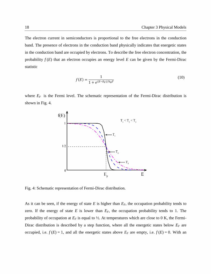
3.2 Bandgap energy and its temperature dependence
The bandgap energy EG is the energy defined as the difference between the bottom of the
conduction band EC and the top of the valence band EV :
𝐸𝐺 = 𝐸𝐶 − 𝐸𝑉 (15)
20 Chapter 3 Physical Models
The value of the bandgap is strongly affected by temperature. An increase in temperature leads to
a decrease of the bandgap. Considering that the bandgap variation affects also the parameters
which depend on it, an appropriate model has to be included for accurate device simulation.
To describe the temperature dependence of semiconductor bandgaps, the function
𝐸𝐺 = 𝐸𝐺(0) −𝛼𝑇2
(𝑇 + 𝛽)
(16)
can be applied [30,34], where EG (0) is the bandgap energy at 0 K, and α and β fitting parameters.
For 4H-SiC the bandgap energy EG (0) is 3.26 eV [35], α and β are 6.5·10-4
eV/K and 1300 K,
respectively [33]. The calculated temperature dependence of the 4H-SiC bandgap is shown in
Fig. 5.
Fig. 5: Bandgap energy of 4H-SiC as a function of temperature.
3.3 Incomplete ionization 21
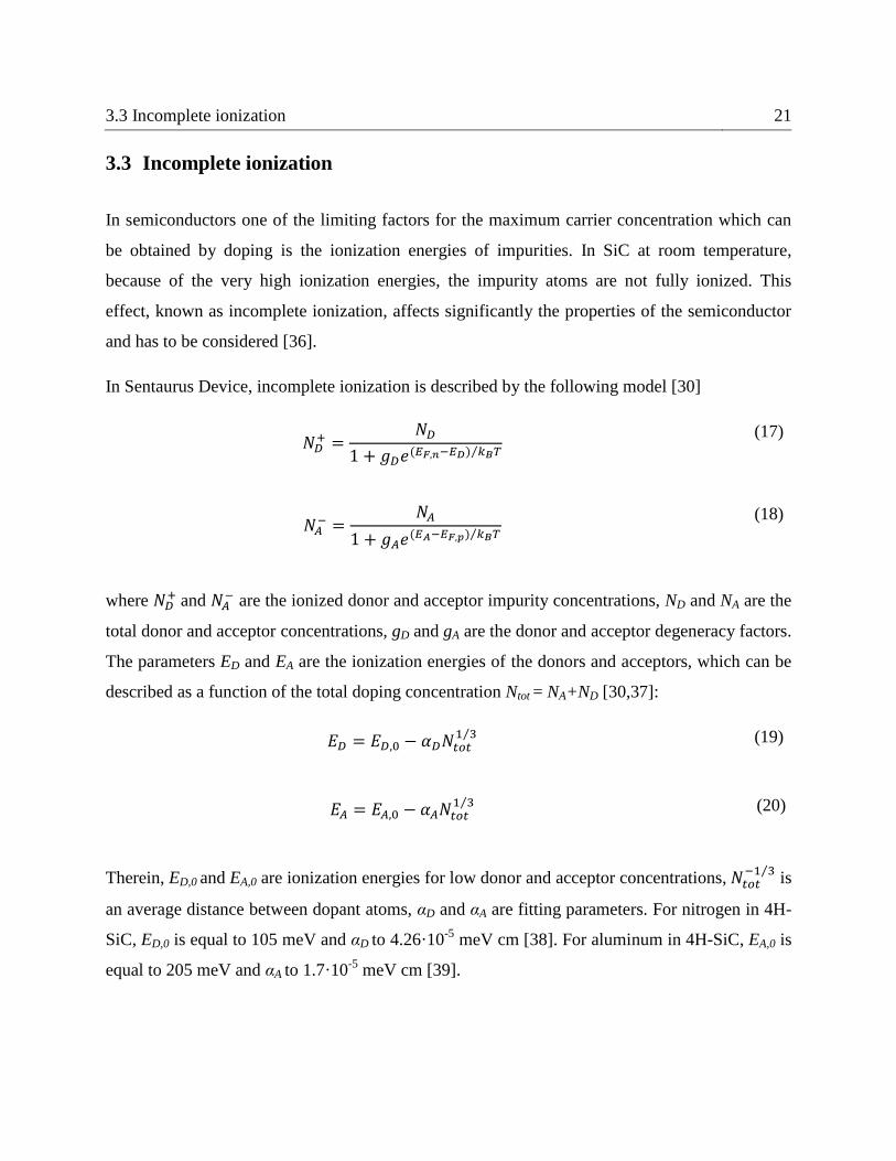
3.3 Incomplete ionization
In semiconductors one of the limiting factors for the maximum carrier concentration which can
be obtained by doping is the ionization energies of impurities. In SiC at room temperature,
because of the very high ionization energies, the impurity atoms are not fully ionized. This
effect, known as incomplete ionization, affects significantly the properties of the semiconductor
and has to be considered [36].
In Sentaurus Device, incomplete ionization is described by the following model [30]
𝑁𝐷+ =
𝑁𝐷
1 + 𝑔𝐷𝑒(𝐸𝐹,𝑛−𝐸𝐷) 𝑘𝐵𝑇⁄
(17)
𝑁𝐴− =
𝑁𝐴
1 + 𝑔𝐴𝑒(𝐸𝐴−𝐸𝐹,𝑝) 𝑘𝐵𝑇⁄
(18)
where 𝑁𝐷+ and 𝑁𝐴
− are the ionized donor and acceptor impurity concentrations, ND and NA are the
total donor and acceptor concentrations, gD and gA are the donor and acceptor degeneracy factors.
The parameters ED and EA are the ionization energies of the donors and acceptors, which can be
described as a function of the total doping concentration Ntot = NA+ND [30,37]:
𝐸𝐷 = 𝐸𝐷,0 − 𝛼𝐷𝑁𝑡𝑜𝑡1 3⁄
(19)
𝐸𝐴 = 𝐸𝐴,0 − 𝛼𝐴𝑁𝑡𝑜𝑡1 3⁄
(20)
Therein, ED,0 and EA,0 are ionization energies for low donor and acceptor concentrations, 𝑁𝑡𝑜𝑡−1 3⁄
is
an average distance between dopant atoms, αD and αA are fitting parameters. For nitrogen in 4H-
SiC, ED,0 is equal to 105 meV and αD to 4.26·10-5
meV cm [38]. For aluminum in 4H-SiC, EA,0 is
equal to 205 meV and αA to 1.7·10-5
meV cm [39].
22 Chapter 3 Physical Models
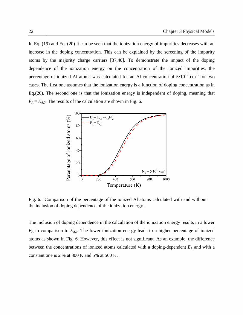
In Eq. (19) and Eq. (20) it can be seen that the ionization energy of impurities decreases with an
increase in the doping concentration. This can be explained by the screening of the impurity
atoms by the majority charge carriers [37,40]. To demonstrate the impact of the doping
dependence of the ionization energy on the concentration of the ionized impurities, the
percentage of ionized Al atoms was calculated for an Al concentration of 5·1017
cm-3
for two
cases. The first one assumes that the ionization energy is a function of doping concentration as in
Eq.(20). The second one is that the ionization energy is independent of doping, meaning that
EA = EA,0. The results of the calculation are shown in Fig. 6.
Fig. 6: Comparison of the percentage of the ionized Al atoms calculated with and without
the inclusion of doping dependence of the ionization energy.
The inclusion of doping dependence in the calculation of the ionization energy results in a lower
EA in comparison to EA,0. The lower ionization energy leads to a higher percentage of ionized
atoms as shown in Fig. 6. However, this effect is not significant. As an example, the difference
between the concentrations of ionized atoms calculated with a doping-dependent EA and with a
constant one is 2 % at 300 K and 5% at 500 K.
3.3 Incomplete ionization 23
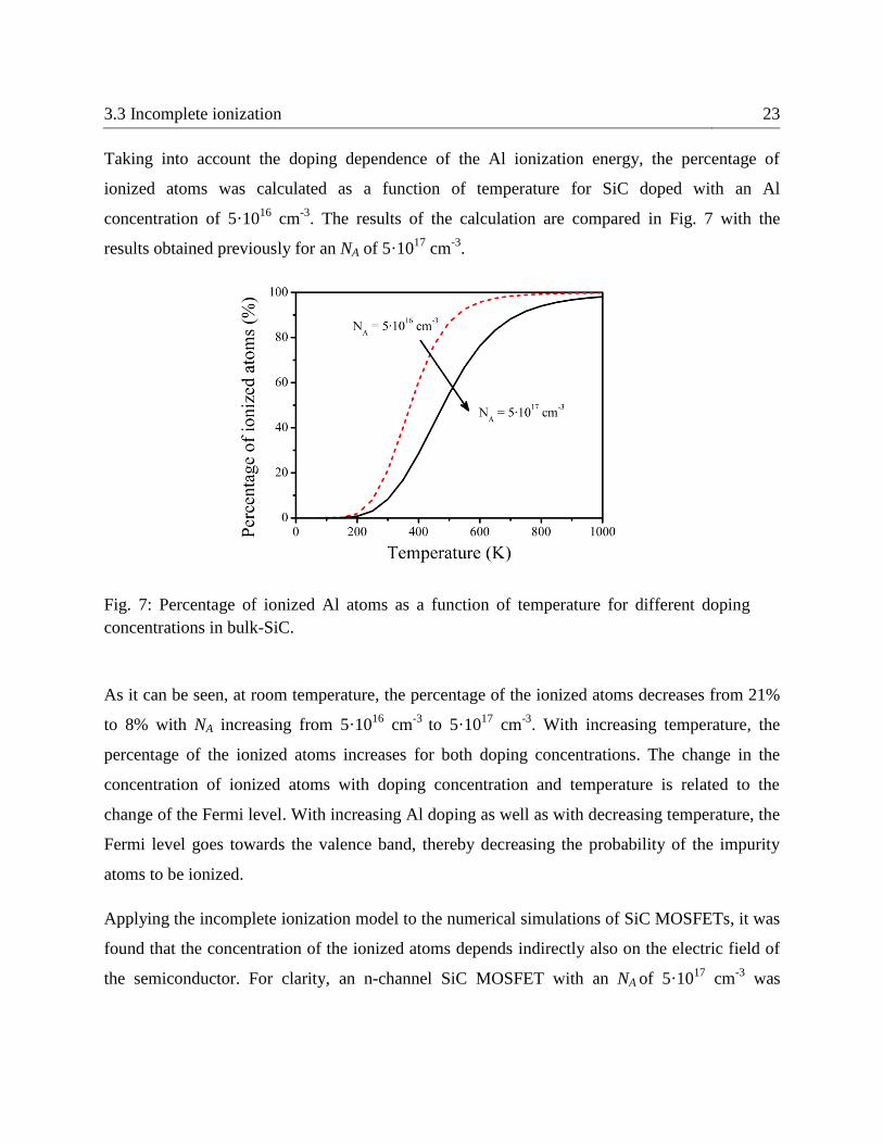
Taking into account the doping dependence of the Al ionization energy, the percentage of
ionized atoms was calculated as a function of temperature for SiC doped with an Al
concentration of 5·1016
cm-3
. The results of the calculation are compared in Fig. 7 with the
results obtained previously for an NA of 5·1017
cm-3
.
Fig. 7: Percentage of ionized Al atoms as a function of temperature for different doping
concentrations in bulk-SiC.
As it can be seen, at room temperature, the percentage of the ionized atoms decreases from 21%
to 8% with NA increasing from 5·1016
cm-3
to 5·1017
cm-3
. With increasing temperature, the
percentage of the ionized atoms increases for both doping concentrations. The change in the
concentration of ionized atoms with doping concentration and temperature is related to the
change of the Fermi level. With increasing Al doping as well as with decreasing temperature, the
Fermi level goes towards the valence band, thereby decreasing the probability of the impurity
atoms to be ionized.
Applying the incomplete ionization model to the numerical simulations of SiC MOSFETs, it was
found that the concentration of the ionized atoms depends indirectly also on the electric field of
the semiconductor. For clarity, an n-channel SiC MOSFET with an NA of 5·1017
cm-3
was
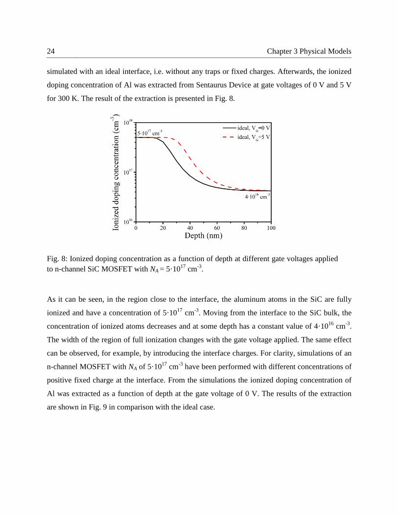
24 Chapter 3 Physical Models
simulated with an ideal interface, i.e. without any traps or fixed charges. Afterwards, the ionized
doping concentration of Al was extracted from Sentaurus Device at gate voltages of 0 V and 5 V
for 300 K. The result of the extraction is presented in Fig. 8.
Fig. 8: Ionized doping concentration as a function of depth at different gate voltages applied
to n-channel SiC MOSFET with NA = 5·1017
cm-3
.
As it can be seen, in the region close to the interface, the aluminum atoms in the SiC are fully
ionized and have a concentration of 5·1017
cm-3
. Moving from the interface to the SiC bulk, the
concentration of ionized atoms decreases and at some depth has a constant value of 4·1016
cm-3
.
The width of the region of full ionization changes with the gate voltage applied. The same effect
can be observed, for example, by introducing the interface charges. For clarity, simulations of an
n-channel MOSFET with NA of 5·1017
cm-3
have been performed with different concentrations of
positive fixed charge at the interface. From the simulations the ionized doping concentration of
Al was extracted as a function of depth at the gate voltage of 0 V. The results of the extraction
are shown in Fig. 9 in comparison with the ideal case.
3.3 Incomplete ionization 25
Fig. 9: Ionized doping concentration as a function of depth at VG = 0 V applied to n-channel SiC
MOSFET with NA = 5·1017
cm-3
and different concentrations QF of fixed charge.
As it can be seen, the width of the region of full ionization increases with an increase in the
concentration of the positive fixed charge. In comparison with the ideal case the change in the
width is insignificant if QF is low, 1·1011
cm-2
. The effects of full ionization of the impurity
atoms in MOSFETs with an ideal interface at gate voltages of 0 V and 5 V as well as in the
MOSFETs with different concentrations of fixed charge can be explained as follows. In SiC n-
channel MOSFETs with an ideal interface, due to the work-function difference between
semiconductor and gate material, the energy bands bend slightly downward even at 0 V. This
results in an electric field which leads to a depletion of holes at the interface. Applying a larger
positive voltage, the bands bend even more downward increasing the electric field at the
interface. This results in a stronger depletion of holes and an accumulation of electrons at the
interface. The same effect is obtained by introducing different sheet concentrations of the
positive fixed charge. The higher its concentration, the larger the electric field at the interface.
Considering that the concentration of holes is related to the quasi-Fermi level as
𝑝~𝑒𝑥𝑝(𝐸𝑉−𝐸𝐹,𝑝
𝑘𝐵𝑇), the concentration of the ionized acceptors can be described in terms of the hole
concentration instead of the quasi-Fermi level:
26 Chapter 3 Physical Models
𝑁𝐴− =
𝑁𝐴
1 + 𝑔𝐴𝑝
𝑁𝑉𝑒(−𝐸𝐴−𝐸𝑉𝑘𝐵𝑇
)
(21)
In Eq. (21) it can be seen that the depletion of holes leads to a full ionization of impurity atoms at
the interface. The wider the depletion region, the wider the region of full ionization. This allows
to conclude that in n-channel SiC MOSFETs the properties of the semiconductor near the
interface are not affected by incomplete ionization. However, the effect of incomplete ionization
has to be considered in the bulk.
3.4 Near-Interface Trap model
3.4.1 The fundamental knowledge of traps
The quality of the SiC/SiO2 interface is a critical factor for the performance of 4H-SiC
MOSFETs with a surface channel. It is mainly determined by the charges located at the interface
or in the oxide. A thermally grown SiO2 contains different kinds of charges. The presence of
carbon during oxidation of SiC leads to a higher concentration of defects at the interface in
comparison to the oxidation of Si. However, the main kinds of charges in SiO2 are the same for
Si and SiC. A schematic representation of the charges associated with the thermally grown SiO2
on SiC is shown in Fig. 10 [41,42], where all the oxide charges are classified as:
Mobile ion charges – positive charges within the oxide associated with the incorporation
of such atoms as sodium (Na) and potassium (K) during the oxidation process [43]. Being
presented in the oxide, they can diffuse to the interface during the operation of MOS-
devices and produce a threshold voltage shift.
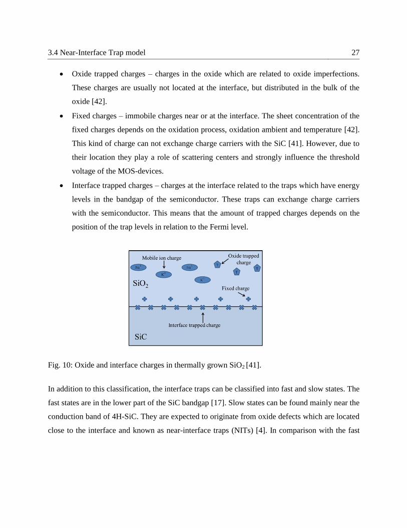
3.4 Near-Interface Trap model 27
Oxide trapped charges – charges in the oxide which are related to oxide imperfections.
These charges are usually not located at the interface, but distributed in the bulk of the
oxide [42].
Fixed charges – immobile charges near or at the interface. The sheet concentration of the
fixed charges depends on the oxidation process, oxidation ambient and temperature [42].
This kind of charge can not exchange charge carriers with the SiC [41]. However, due to
their location they play a role of scattering centers and strongly influence the threshold
voltage of the MOS-devices.
Interface trapped charges – charges at the interface related to the traps which have energy
levels in the bandgap of the semiconductor. These traps can exchange charge carriers
with the semiconductor. This means that the amount of trapped charges depends on the
position of the trap levels in relation to the Fermi level.
Fig. 10: Oxide and interface charges in thermally grown SiO2 [41].
In addition to this classification, the interface traps can be classified into fast and slow states. The
fast states are in the lower part of the SiC bandgap [17]. Slow states can be found mainly near the
conduction band of 4H-SiC. They are expected to originate from oxide defects which are located
close to the interface and known as near-interface traps (NITs) [4]. In comparison with the fast

28 Chapter 3 Physical Models
states, the slow states have a more crucial impact on the performance of n-channel SiC
MOSFETs and are needed to be accurately characterized.
Naturally, interface traps can be donor-like and acceptor-like states. The behavior of the traps is
considered to be similar to the doping impurities [41]. The charge states of donor and acceptor
traps are changed in dependence on the Fermi level as shown in Fig. 11.
Fig. 11: Change of charge state of traps in dependence on the Fermi level.
Donor traps with levels above the Fermi level are positively charged and donate electrons to the
conduction band. As soon as they fall below the Fermi level, donor traps become occupied and
change their charge state from positive to neutral. For acceptor traps, the dependence on the
Fermi level is opposite. All the traps with levels above the Fermi level are neutral. When they
fall below the Fermi level, they accept (trap) electrons and, thereby, change their charge state
from neutral to negative.
To understand the impact of donor and acceptor traps on the electrical characteristics of
MOSFETs, an analysis of positively and negatively charged traps has been performed with
Sentaurus Device. For this purpose, firstly, current-voltage characteristics were computed using
the default simulation model that assumes an ideal SiC/SiO2 interface. To demonstrate the
impact of negatively charged interface traps, acceptor traps with a concentration of 2·1012
cm-2
and a level 50 meV below the 4H-SiC conduction band were added to the ideal interface. A
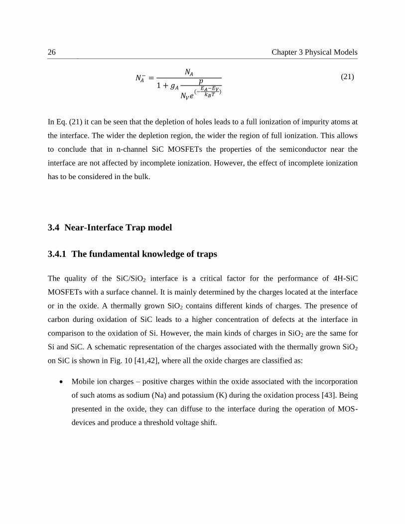
3.4 Near-Interface Trap model 29
comparison between the current-voltage characteristics simulated assuming an ideal interface
and in presence of the acceptor traps at the interface is shown in Fig. 12.
Fig. 12: Impact of acceptor traps on the current-voltage characteristics of SiC MOSFETs. The
acceptor traps have been simulated with a concentration of 2·1012
cm-2
and a level of 50 meV
below EC.
The negatively charged acceptor traps have several effects on the device performance. The first
effect is a trapping of electrons from the inversion layer, excluding them from participating in the
electronic transport in the transistor channel. The second effect is a shift of the threshold voltage
of n-channel MOSFETs to higher values. The third effect is the scattering of electrons in the
inversion layer at the negatively charged centers. The latter leads to a reduction of the mobility
of the electrons in the inversion layer. All these effects contribute to the decrease of the
MOSFET drain current and enlarge the threshold voltage in comparison with the ideal
MOSFETs behavior without any traps.
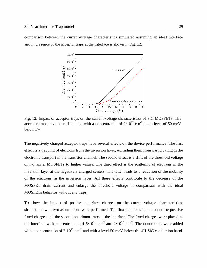
To show the impact of positive interface charges on the current-voltage characteristics,
simulations with two assumptions were performed. The first one takes into account the positive
fixed charges and the second one donor traps at the interface. The fixed charges were placed at
the interface with concentrations of 5·1011
cm-2
and 2·1012
cm-2
. The donor traps were added
with a concentration of 2·1012
cm-2
and with a level 50 meV below the 4H-SiC conduction band.
30 Chapter 3 Physical Models
A comparison between the simulation assuming an ideal interface and simulations with positive
charges at the interface are shown in Fig. 13.
Fig. 13: Impact of positive fixed charges (left) and donor traps (right) on the current-voltage
characteristics of SiC MOSFET. The donor traps have been simulated with a concentration of
2·1012
cm-2
and a level of 50 meV below EC.
In n-channel MOSFETs positive charges, either fixed charges or donor traps, act as scattering
centers. However, in contrast to acceptor traps, their presence leads to a decrease of the threshold
voltage VTH. Despite the same effect of a decrease in VTH, there is also a difference between the
behavior of fixed charges and donor traps. As it was mentioned above, fixed charges do not
depend on the Fermi level. The presence of positive fixed charges at the interface produces only
a parallel shift of the threshold voltage to lower values, thereby increasing the MOSFET drain
current. The higher the concentration of the positive fixed charge, the lower the threshold
voltage. Donor traps being above the Fermi level also decrease the threshold voltage, providing
positive charges at the interface. However, after they fall below the Fermi level, donor traps
become neutral and do not affect the MOSFET drain current. Assuming the presence of only
donor traps and considering that the Fermi level depends on gate voltage, this means that at some
gate voltages when all donor traps are occupied, the drain current is the same as the one
simulated with an ideal interface.
3.4 Near-Interface Trap model 31
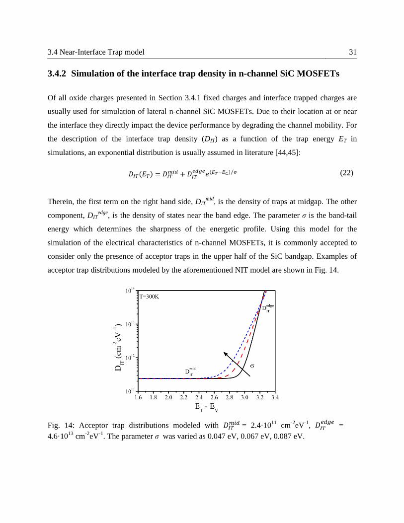
3.4.2 Simulation of the interface trap density in n-channel SiC MOSFETs
Of all oxide charges presented in Section 3.4.1 fixed charges and interface trapped charges are
usually used for simulation of lateral n-channel SiC MOSFETs. Due to their location at or near
the interface they directly impact the device performance by degrading the channel mobility. For
the description of the interface trap density (DIT) as a function of the trap energy ET in
simulations, an exponential distribution is usually assumed in literature [44,45]:
𝐷𝐼𝑇(𝐸𝑇) = 𝐷𝐼𝑇𝑚𝑖𝑑 + 𝐷𝐼𝑇
𝑒𝑑𝑔𝑒𝑒(𝐸𝑇−𝐸𝐶) 𝜎⁄ (22)
Therein, the first term on the right hand side, DITmid
, is the density of traps at midgap. The other
component, DITedge
, is the density of states near the band edge. The parameter σ is the band-tail
energy which determines the sharpness of the energetic profile. Using this model for the
simulation of the electrical characteristics of n-channel MOSFETs, it is commonly accepted to
consider only the presence of acceptor traps in the upper half of the SiC bandgap. Examples of
acceptor trap distributions modeled by the aforementioned NIT model are shown in Fig. 14.
Fig. 14: Acceptor trap distributions modeled with 𝐷𝐼𝑇𝑚𝑖𝑑 = 2.4·10
11 cm
-2eV
-1, 𝐷𝐼𝑇
𝑒𝑑𝑔𝑒 =
4.6·1013
cm-2
eV-1
. The parameter σ was varied as 0.047 eV, 0.067 eV, 0.087 eV.
32 Chapter 3 Physical Models
It should be noted that the parameters in the current model have well-defined meanings.
However, they are usually just fitting parameters to reproduce some characteristics of the
electrical behavior of MOSFETs. To avoid inaccuracies in simulations associated with the NIT
model described in Eq. (22), the interface trap density can be extracted from Hall-effect and C-V
measurements. This method of extraction of the interface trap density from electrical
measurements is self-consistent in the sense that it describes such properties of the interface as
the trapping of the electrons in the NITs. The results of the DIT(ET) extraction from C-V and
Hall-effect measurements are often combined. It is known that the DIT(ET) distribution from the
Hall-effect method can be obtained only when the MOS device is in inversion [46]. Considering
this condition, the minimum energy of the DIT distribution can be given as EC – ~ 0.1 eV and
EC – ~ 0.26 eV for the MOSFETs with the background doping concentrations NA of 5·1017
cm-3
and 1·1015
cm-3
, respectively. The part of the DIT (ET) distribution at lower trap energies can be
determined from C-V measurements. This method, as opposite to the Hall-effect one, allows to
determine accurately DIT (ET) closer to the center of the bandgap, but near the band-edge it gives
large errors [46,47]. The limitation in the determination of the energetic position of the interface
traps from the Hall-effect and capacitance-voltage measurements is the main reason for the
combination of the DIT (ET) distributions extracted from the aforementioned measurements.
In this work, to characterize SiC MOSFETs by numerical simulations, NIT model was developed
on the basis of the DIT (ET) extraction from Hall-effect and capacitance-voltage measurements
with a subsequent numerical optimization of the extracted distributions. To develop the NIT
model for all studied samples, #E1, #E2, #W1 and #W2, the following steps have been done:
Extraction of DIT (ET) near the conduction band from Hall-effect measurements
Extraction of DIT (ET) at lower trap energies from C-V measurements
Introduction of the extracted energetic profiles of the interface traps as initial
distributions into Sentaurus Device via a table function
Optimization of DIT (ET) by the reproduction of the current-voltage (ID (VG)) and Hall-
effect measurements (ninv (VG), 𝜇 (VG)) in the numerical simulations
3.4 Near-Interface Trap model 33
To extract DIT (ET) from Hall-effect measurements, C++ scripts have been written based on the
method described in Chapter 4. It should be noted that the scripts used in the calculations assume
simplified models, for example, step function for the probability of trap occupation, neglect of
potential drop along the channel from source to drain as well as of field dependence of the
ionization of impurity atoms. The introduction of the initial DIT (ET) distributions, calculated
using C++ scripts, into Sentaurus Device, for instance, for the simulation of the drain currents
led to deviations between simulations and measurements. The reason of the deviations can be
explained by the usage of simplified models in the scripts for the extraction of the DIT (ET)
distributions. To minimize the deviations, a numerical optimization has been performed. The
optimization in Sentaurus Device has been done considering that the position of the Fermi level
and, as a consequence the occupation of traps, is related to the gate voltage applied. Taking this
into account, the initial DIT (ET) distributions, extracted from Hall-effect and C-V measurements
and implemented in the simulations via table functions, have been corrected at certain gate
voltages to reproduce the set of measurements, i. e. the drain currents, sheet carrier density and
channel mobility as a function of gate voltage. Additionally, the DIT (ET) distributions, extracted
from Hall-effect measurements, have been adjusted using the newly calculated Hall factor in the
channel of the studied MOSFETs described in Chapter 6. The process of the optimization of the
initial DIT (ET) distributions is summarized in Fig. 15.
Here it should be noted that the extraction of the DIT (ET) distribution only from experimental
data can be considered as a conventional method which is used in literature for the
characterization of the interface traps. However, an accuracy of this method is limited by the
simplified assumptions, as it was discussed above. Thus, it is expected that the method suggested
in this work, which accounts also for the numerical optimization of DIT (ET) by the comparison
between the set of simulations and measurements, gives physically more reasonable results for
the extracted DIT (ET) distributions.
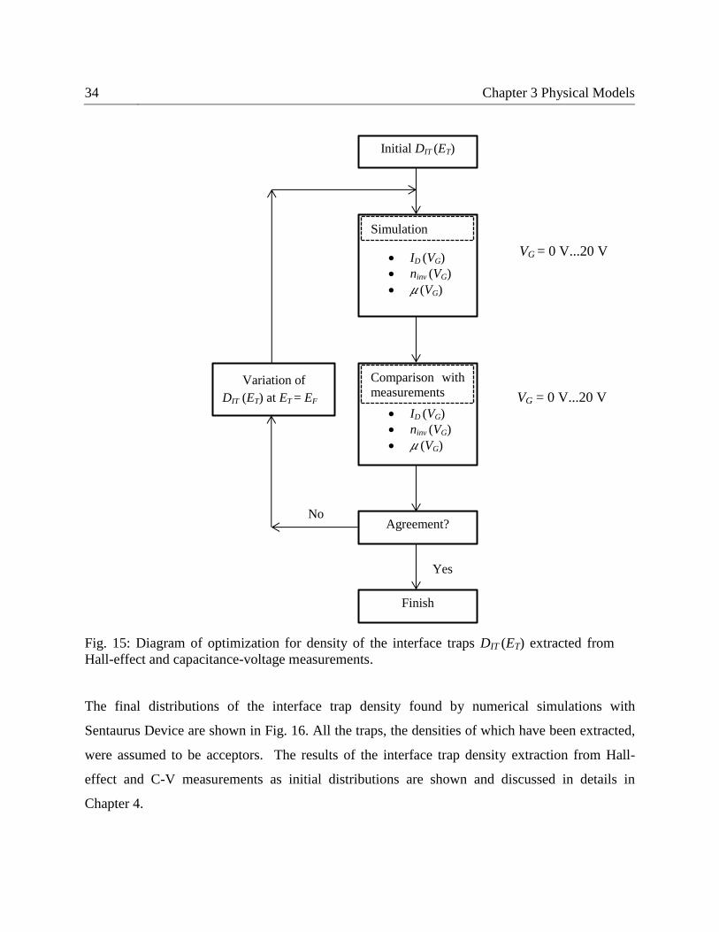
34 Chapter 3 Physical Models
VG = 0 V...20 V
VG = 0 V...20 V
Fig. 15: Diagram of optimization for density of the interface traps DIT (ET) extracted from
Hall-effect and capacitance-voltage measurements.
The final distributions of the interface trap density found by numerical simulations with
Sentaurus Device are shown in Fig. 16. All the traps, the densities of which have been extracted,
were assumed to be acceptors. The results of the interface trap density extraction from Hall-
effect and C-V measurements as initial distributions are shown and discussed in details in
Chapter 4.
Yes
No
Initial DIT (ET)
ID (VG)
ninv (VG)
𝜇 (VG)
Simulation
ID (VG)
ninv (VG)
𝜇 (VG)
Comparison with
measurements
Agreement?
Finish
Variation of
DIT (ET) at ET = EF
3.4 Near-Interface Trap model 35
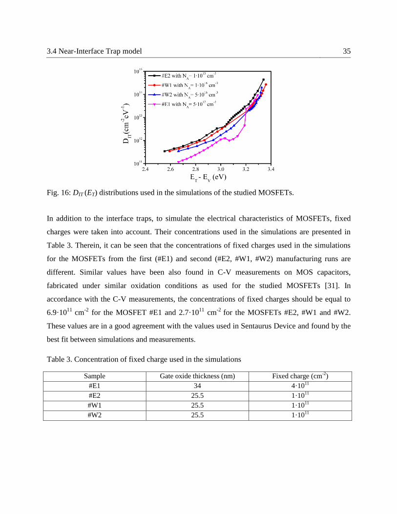
Fig. 16: DIT (ET) distributions used in the simulations of the studied MOSFETs.
In addition to the interface traps, to simulate the electrical characteristics of MOSFETs, fixed
charges were taken into account. Their concentrations used in the simulations are presented in
Table 3. Therein, it can be seen that the concentrations of fixed charges used in the simulations
for the MOSFETs from the first (#E1) and second (#E2, #W1, #W2) manufacturing runs are
different. Similar values have been also found in C-V measurements on MOS capacitors,
fabricated under similar oxidation conditions as used for the studied MOSFETs [31]. In
accordance with the C-V measurements, the concentrations of fixed charges should be equal to
6.9·1011
cm-2
for the MOSFET #E1 and 2.7·1011
cm-2
for the MOSFETs #E2, #W1 and #W2.
These values are in a good agreement with the values used in Sentaurus Device and found by the
best fit between simulations and measurements.
Table 3. Concentration of fixed charge used in the simulations
Sample Gate oxide thickness (nm) Fixed charge (cm-2
)
#E1 34 4·1011
#E2 25.5 1·1011
#W1 25.5 1·1011
#W2 25.5 1·1011
36 Chapter 3 Physical Models
3.5 Mobility degradation model
It is widely accepted that the channel mobility in lateral SiC MOSFETs can be modeled as a
combination of the mobility components associated with the following scattering mechanisms:
Coulomb scattering at ionized impurities in the bulk (µIMP);
Coulomb scattering at the interface charges (µC);
surface-roughness scattering (µSR);
surface-phonon scattering (µSP);
bulk-phonon scattering (𝜇BP);
Assuming the scattering mechanisms to be independent of each other, the total channel mobility
can be calculated by Matthiessen’s rule as [44,48,49]
𝜇 = (1
𝜇𝐼𝑀𝑃+1
𝜇𝐶+1
𝜇𝑆𝑅+1
𝜇𝑆𝑃+1
𝜇𝐵𝑃)−1
(23)
In Eq. (23) 𝜇IMP and 𝜇BP are the mobility components which determine the total mobility in the
bulk 𝜇B. Assuming again Matthiessen’s rule 𝜇B can be given by
𝜇𝐵 = (1
𝜇𝐼𝑀𝑃+1
𝜇𝐵𝑃)−1
(24)
To simulate the temperature dependence of the electrical characteristics of the studied MOSFETs
with low and high background doping concentrations, a new model for the bulk mobility 𝜇B was
developed on the basis of the conventional one [50,51,52,53] and implemented into Sentaurus
Device via “Physical Model Interface (PMI)” in the form
𝜇𝐵 = 𝜇𝑚𝑖𝑛 (𝑇
300𝐾)𝛼
+𝜇𝐵𝑃1 (
𝑇300𝐾)
ξ
+ 𝜇𝐵𝑃2 (𝑇
300𝐾)ϰ
− 𝜇𝑚𝑖𝑛 (𝑇
300𝐾)α
1 + (𝑇
300𝐾)ϑ
(𝑁𝐴−
𝑁𝑟𝑒𝑓)
𝑧
(25)

3.5 Mobility degradation model 37
Therein, 𝜇min is the mobility in highly doped material, where Coulomb scattering at the ionized
impurities is dominant, 𝜇BP1 and 𝜇BP2 are components of the mobility in lightly doped material,
where bulk-phonon scattering is the main scattering mechanism, Nref, 𝛼, 𝜉, 𝜘, 𝜗, z are fitting
parameters. The values of the model parameters used in the simulations are summarized in Table
4. A detailed description of the model and its calibration will be given in Section 6.4, where the
temperature dependence of the electrical characteristics of SiC MOSFETs will be discussed.
Table 4. Parameter values for bulk mobility component (𝜇B)
Parameter Value Unit
𝜇min 40 cm2/Vs
𝜇BP1 500 cm2/Vs
𝜇BP2 450 cm2/Vs
Nref 2·1017
cm-3
𝛼 -0.5 1
𝜉 -11.6 1
𝜘 -2.74 1
𝜗 -12.5 1
z 0.76 1
In lateral n-channel 4H-SiC MOSFETs Coulomb scattering at the interface charges is the
dominant scattering mechanism due to the high density of interface traps. Taking this into
account, the model for the mobility component 𝜇C is one of the most important models in the
simulations of the electrical characteristics of MOSFETs. In Sentaurus Device this model is
included in the form [30]
𝜇𝐶 =
𝜇1 (𝑇
300𝐾){1 + [𝑛 (𝑛𝑡𝑟𝑎𝑛𝑠 (𝑁𝑐𝑁0)η1
)⁄ ]
𝜐
}
(𝑁𝑐𝑁0)η2
· 𝐷(𝑥) · 𝑓(ℰ⟘)
(26)
where µ1 is a fitting parameter, n is the concentration of electrons near the interface, Nc is the
interface charge density, x is a distance from the interface, Ɛ⟘ is the electric field perpendicular to
the oxide/semiconductor interface. The functions D (x) and f (Ɛ⟘) are given by [30]:
38 Chapter 3 Physical Models
𝐷 = 𝑒(−𝑥/𝑙𝑐𝑟𝑖𝑡) (27)
𝑓(ℰ⟘) = 1 − 𝑒[−(ℰ⟘ 𝐸0)⁄ 𝛾
] (28)
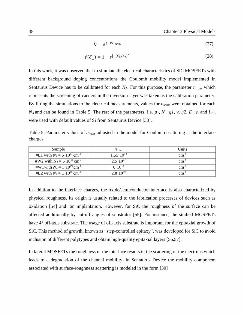
In this work, it was observed that to simulate the electrical characteristics of SiC MOSFETs with
different background doping concentrations the Coulomb mobility model implemented in
Sentaurus Device has to be calibrated for each NA. For this purpose, the parameter ntrans which
represents the screening of carriers in the inversion layer was taken as the calibration parameter.
By fitting the simulations to the electrical measurements, values for ntrans were obtained for each
NA and can be found in Table 5. The rest of the parameters, i.e. µ1, N0, η1, ν, η2, E0, γ, and lcrit,
were used with default values of Si from Sentaurus Device [30].
Table 5. Parameter values of ntrans adjusted in the model for Coulomb scattering at the interface
charges
Sample ntrans Units
#E1 with NA = 5·1017
cm-3
1.55·1018
cm-3
#W2 with NA = 5·1016
cm-3
2.5·1017
cm-3
#W1with NA = 1·1016
cm-3
8·1016
cm-3
#E2 with NA = 1·1015
cm-3
2.8·1016
cm-3
In addition to the interface charges, the oxide/semiconductor interface is also characterized by
physical roughness. Its origin is usually related to the fabrication processes of devices such as
oxidation [54] and ion implantation. However, for SiC the roughness of the surface can be
affected additionally by cut-off angles of substrates [55]. For instance, the studied MOSFETs
have 4° off-axis substrate. The usage of off-axis substrate is important for the epitaxial growth of
SiC. This method of growth, known as “step-controlled epitaxy”, was developed for SiC to avoid
inclusion of different polytypes and obtain high-quality epitaxial layers [56,57].
In lateral MOSFETs the roughness of the interface results in the scattering of the electrons which
leads to a degradation of the channel mobility. In Sentaurus Device the mobility component
associated with surface-roughness scattering is modeled in the form [30]

3.5 Mobility degradation model 39
𝜇𝑆𝑅 = {(ℰ⟘ ℰ𝑟𝑒𝑓⁄ )
2
𝛿+ℰ⟘3
η}
−1
1
𝐷
(29)
where Ɛ ref is the reference field equal to 1 V/cm, δ and η are fit parameters which depend on
the roughness of the SiC/SiO2 interface and account for such interface characteristics as
correlation length and average step height [58,48]. From Eq. (29) it can be seen that the higher
the values of δ and η, the higher the mobility 𝜇SR which indicates a lower roughness of the
surface.
Considering the dependence of 𝜇SR on the electric field, the contribution of surface-roughness
scattering to the channel mobility is stronger at higher gate voltages. Taking this into account, δ
and η were modified in the current work from the Si default values by bringing the simulated and
experimental current-voltage characteristics at higher gate voltages into agreement. The values of
δ and η used in the simulations are shown in Table 6. Therein, it can be seen that the fitting
parameters for the MOSFETs from the first (#E1) and second (#E2, #W1, #W2) manufacturing
runs differ almost by a factor of 10. The simulation results reveal that the interface is rougher for
the MOSFET #E1 which has a thicker oxide and a thicker epitaxial layer. This result is in
agreement with the works [54,59,60] in which it was shown that surface roughness increases
with an increase in the oxide thickness as well as with an increase in the thickness of the
epitaxial layer.
Table 6. Parameter values for the surface-roughness mobility component (𝜇SR)
Parameter Value for #E1 with
Tox = 34 nm
Value for #E2, #W1,
#W2 with Tox = 25.5 nm
Units
δ 1.7∙1013
1.6∙1014
cm2/(V∙s)
η 1.7∙1029
1.6∙1030
V2/(cm∙s)
In addition to the scattering mechanisms discussed above, the contribution attributed to surface-
phonon scattering is modeled in Sentaurus Device by [30]
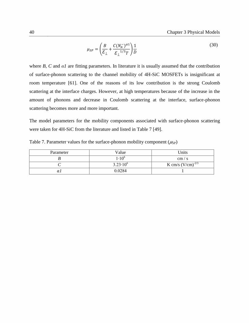
40 Chapter 3 Physical Models
𝜇𝑆𝑃 = (𝐵
ℰ⟘+𝐶(𝑁𝐴
−)𝛼1
ℰ⟘1 3⁄𝑇)1
𝐷
(30)
where B, C and α1 are fitting parameters. In literature it is usually assumed that the contribution
of surface-phonon scattering to the channel mobility of 4H-SiC MOSFETs is insignificant at
room temperature [61]. One of the reasons of its low contribution is the strong Coulomb
scattering at the interface charges. However, at high temperatures because of the increase in the
amount of phonons and decrease in Coulomb scattering at the interface, surface-phonon
scattering becomes more and more important.
The model parameters for the mobility components associated with surface-phonon scattering
were taken for 4H-SiC from the literature and listed in Table 7 [49].
Table 7. Parameter values for the surface-phonon mobility component (𝜇SP)
Parameter Value Units
B 1∙106 cm / s
C 3.23∙106 K cm/s (V/cm)
-2/3
𝑎1 0.0284 1

41
Chapter 4 Extraction of the Density of Interface
Traps from Electrical Measurements
The occupation of the interface traps and, as a consequence the interface trapped charge (QIT), is
determined by the position of the Fermi level in relation to the energy levels of traps. In MOS
devices the Fermi level can be controlled by the gate voltage applied. This means, when the gate
voltage changes, the interface trapped charge also changes. Considering that energy levels of
interface traps are distributed across the bandgap, their density (DIT) is defined as number of
charges per unit area and unit energy difference in the bandgap [41]
𝐷𝐼𝑇 = 1
𝑞
𝑑𝑄𝐼𝑇𝑑𝐸
(31)
The change of the interface trapped charge with gate voltage is the basis for the DIT
determination from experimental methods such as Hall-effect and capacitance-voltage
measurements.
4.1 Hall-effect measurements
From semiconductor theory it is known that the gate voltage applied to MOSFETs with an ideal
interface, i.e. no interface charges, is balanced by a space charge induced by the electric field.
Assuming a source-drain voltage VD equal to 0 V the charge balance for n-channel MOSFETs
with ideal interface can be expressed by [41]
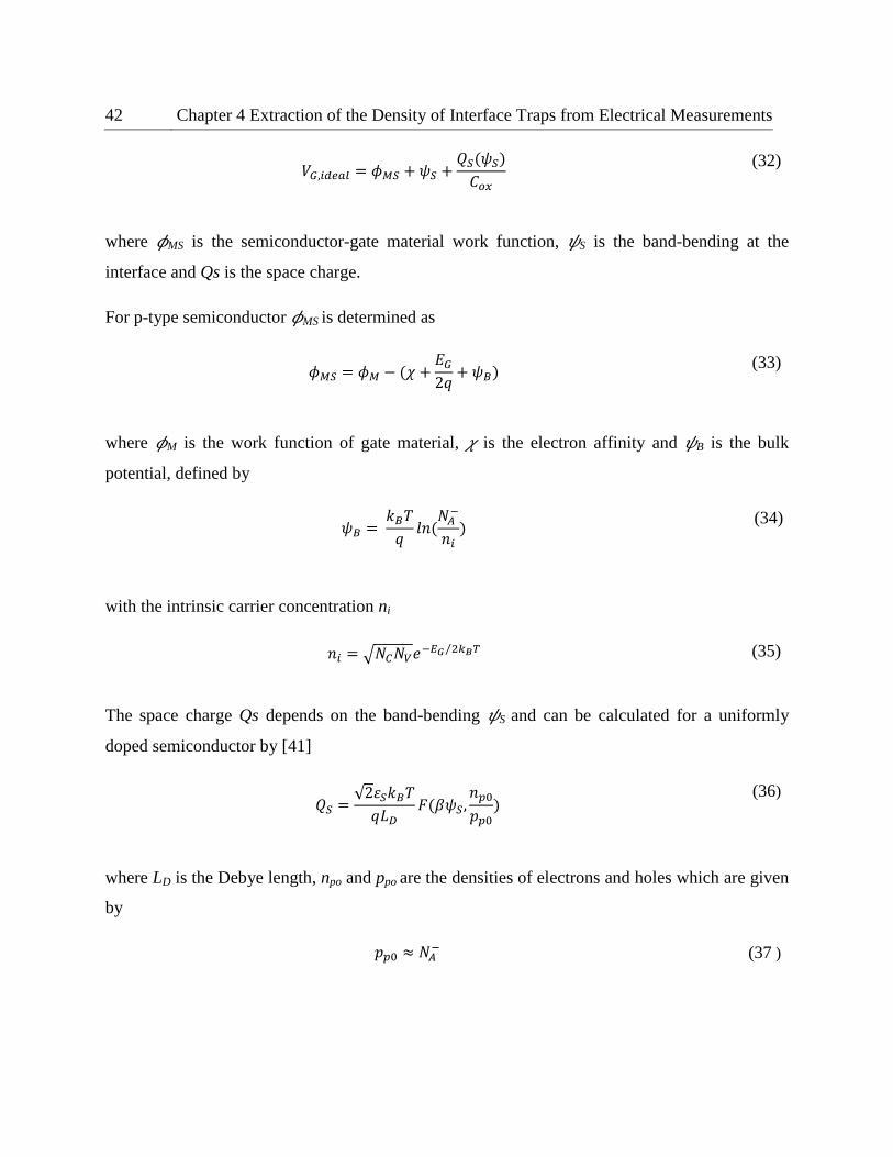
42 Chapter 4 Extraction of the Density of Interface Traps from Electrical Measurements
𝑉𝐺,𝑖𝑑𝑒𝑎𝑙 = 𝜙𝑀𝑆 + 𝜓𝑆 +𝑄𝑆(𝜓𝑆)
𝐶𝑜𝑥
(32)
where 𝜙MS is the semiconductor-gate material work function, 𝜓S is the band-bending at the
interface and Qs is the space charge.
For p-type semiconductor 𝜙MS is determined as
𝜙𝑀𝑆 = 𝜙𝑀 − (𝜒 +𝐸𝐺2𝑞+ 𝜓𝐵)
(33)
where 𝜙M is the work function of gate material, 𝜒 is the electron affinity and 𝜓B is the bulk
potential, defined by
𝜓𝐵 = 𝑘𝐵𝑇
𝑞𝑙𝑛(𝑁𝐴−
𝑛𝑖)
(34)
with the intrinsic carrier concentration ni
𝑛𝑖 = √𝑁𝐶𝑁𝑉𝑒−𝐸𝐺 2𝑘𝐵𝑇⁄ (35)
The space charge Qs depends on the band-bending 𝜓S and can be calculated for a uniformly
doped semiconductor by [41]
𝑄𝑆 =√2휀𝑆𝑘𝐵𝑇
𝑞𝐿𝐷𝐹(𝛽𝜓𝑆,
𝑛𝑝0𝑝𝑝0)
(36)
where LD is the Debye length, npo and ppo are the densities of electrons and holes which are given
by
𝑝𝑝0 ≈ 𝑁𝐴− (37 )
4.1 Hall-effect measurements 43
𝑛𝑝0 ≅𝑛𝑖2
𝑁𝐴−
(38)
The Debye length and the function 𝐹(𝛽𝜓𝑆,𝑛𝑝0
𝑝𝑝0) are given by [41]
𝐿𝐷 ≡ √𝑘𝐵𝑇휀𝑠𝑝𝑝0𝑞
2
(39)
𝐹 (𝛽𝜓𝑆,𝑛𝑝0
𝑝𝑝0) ≡ √[(𝑒−𝛽𝜓𝑆 + 𝛽𝜓𝑆 − 1) +
𝑛𝑝0
𝑝𝑝0(𝑒𝛽𝜓𝑆 − 𝛽𝜓𝑆 − 1)]
(40)
In reality, the oxide/semiconductor interface is characterized by different types of charges. Their
presence changes the charge balance of the MOSFET in comparison with the ideal one for a
given gate voltage. Considering the influence of the positive fixed charge QF and the interface
trapped charges, where the contributions from acceptor (𝑄𝐼𝑇𝐴 ) and donor (𝑄𝐼𝑇
𝐷 ) traps are
accounted for, Eq.(32) has to be rewritten in the form
𝑉𝐺,𝑟𝑒𝑎𝑙 = 𝜙𝑀𝑆 + 𝜓𝑆 +𝑄𝑆(𝜓𝑆)
𝐶𝑜𝑥+𝑄𝐼𝑇𝐴 (𝜓𝑆)
𝐶𝑜𝑥−𝑄𝐼𝑇𝐷 (𝜓𝑆)
𝐶𝑜𝑥−𝑄𝐹𝐶𝑜𝑥
(41)
Comparing Eq.(32) and Eq.(41), it can be seen that the charges at the interface result in a
difference between the real gate voltage and the ideal one for the same value of 𝜓S. Taking into
account this difference, the density of interface traps can be extracted. A key issue in the
extraction of the DIT (ET) distribution is the determination of the real relation between 𝜓S and VG
which depends on QIT and QF. The usage of Hall-effect measurements allows to determine
𝜓S (VG) directly from the measured sheet carrier density independently of QIT and QF. This is the
main advantage of this method of DIT extraction. When the real and ideal 𝜓S (VG) curves are
determined, the interface trap distribution can be calculated by the difference in the change of the
real and ideal gate voltages required for a small change in Δ𝜓S using Eq. (42) [46]
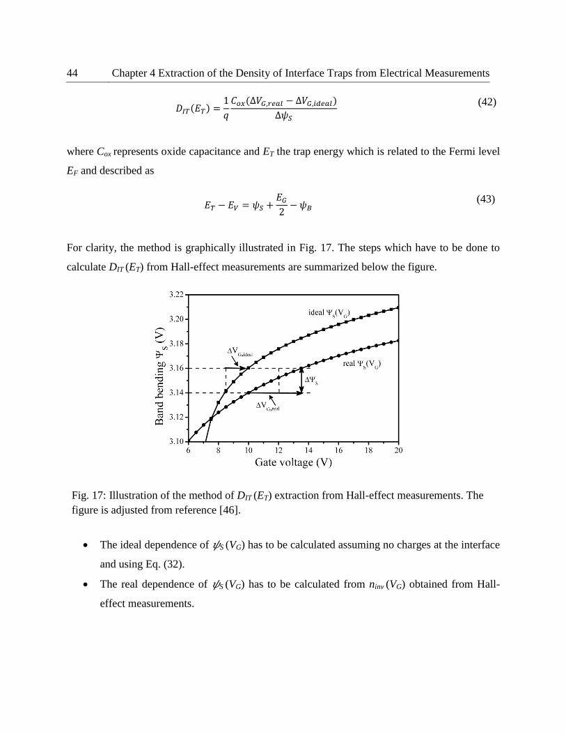
44 Chapter 4 Extraction of the Density of Interface Traps from Electrical Measurements
𝐷𝐼𝑇(𝐸𝑇) =1
𝑞
𝐶𝑜𝑥(∆𝑉𝐺,𝑟𝑒𝑎𝑙 − ∆𝑉𝐺,𝑖𝑑𝑒𝑎𝑙)
∆𝜓𝑆
(42)
where Cox represents oxide capacitance and ET the trap energy which is related to the Fermi level
EF and described as
𝐸𝑇 − 𝐸𝑉 = 𝜓𝑆 +𝐸𝐺2− 𝜓𝐵
(43)
For clarity, the method is graphically illustrated in Fig. 17. The steps which have to be done to
calculate DIT (ET) from Hall-effect measurements are summarized below the figure.
Fig. 17: Illustration of the method of DIT (ET) extraction from Hall-effect measurements. The
figure is adjusted from reference [46].
The ideal dependence of 𝜓S (VG) has to be calculated assuming no charges at the interface
and using Eq. (32).
The real dependence of 𝜓S (VG) has to be calculated from ninv (VG) obtained from Hall-
effect measurements.
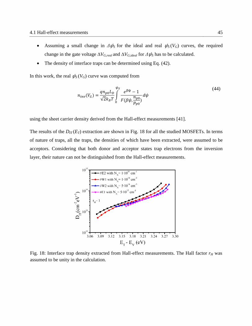
4.1 Hall-effect measurements 45
Assuming a small change in Δ𝜓S for the ideal and real 𝜓S (VG) curves, the required
change in the gate voltage ∆VG,real and ∆VG,ideal for Δ𝜓S has to be calculated.
The density of interface traps can be determined using Eq. (42).
In this work, the real 𝜓S (VG) curve was computed from
𝑛𝑖𝑛𝑣(𝑉𝐺) =𝑞𝑛𝑝0𝐿𝐷
√2𝑘𝐵𝑇∫
𝑒βψ − 1
𝐹(𝛽𝜓,𝑛𝑝0𝑝𝑝0)𝑑𝜓
𝜓𝑆
0
(44)
using the sheet carrier density derived from the Hall-effect measurements [41].
The results of the DIT (ET) extraction are shown in Fig. 18 for all the studied MOSFETs. In terms
of nature of traps, all the traps, the densities of which have been extracted, were assumed to be
acceptors. Considering that both donor and acceptor states trap electrons from the inversion
layer, their nature can not be distinguished from the Hall-effect measurements.
Fig. 18: Interface trap density extracted from Hall-effect measurements. The Hall factor rH was
assumed to be unity in the calculation.
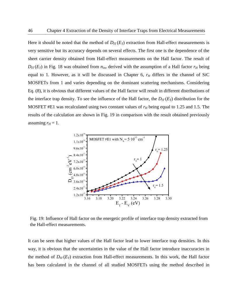
46 Chapter 4 Extraction of the Density of Interface Traps from Electrical Measurements
Here it should be noted that the method of DIT (ET) extraction from Hall-effect measurements is
very sensitive but its accuracy depends on several effects. The first one is the dependence of the
sheet carrier density obtained from Hall-effect measurements on the Hall factor. The result of
DIT (ET) in Fig. 18 was obtained from ninv derived with the assumption of a Hall factor rH being
equal to 1. However, as it will be discussed in Chapter 6, rH differs in the channel of SiC
MOSFETs from 1 and varies depending on the dominant scattering mechanisms. Considering
Eq. (8), it is obvious that different values of the Hall factor will result in different distributions of
the interface trap density. To see the influence of the Hall factor, the DIT (ET) distribution for the
MOSFET #E1 was recalculated using two constant values of rH being equal to 1.25 and 1.5. The
results of the calculation are shown in Fig. 19 in comparison with the result obtained previously
assuming rH = 1.
Fig. 19: Influence of Hall factor on the energetic profile of interface trap density extracted from
the Hall-effect measurements.
It can be seen that higher values of the Hall factor lead to lower interface trap densities. In this
way, it is obvious that the uncertainties in the value of the Hall factor introduce inaccuracies in
the method of DIT (ET) extraction from Hall-effect measurements. In this work, the Hall factor
has been calculated in the channel of all studied MOSFETs using the method described in
4.2 Capacitance-voltage measurements: High-low frequency method 47
Chapter 5. Taking the results of the Hall factor obtained, the DIT (ET) distributions have been
self-consistently determined. The final DIT(ET) distributions, used in the simulations, which take
into account the newly calculated Hall factor have been shown in Fig. 16.
The second effect which may lead to an inaccuracy of the DIT (ET) extraction from Hall-effect
measurements is the accuracy of the determination of 𝜓S (VG). An example can be given on the
basis of the analytical calculation of 𝜓S (VG). It is known that in MOSFETs the band-bending 𝜓S
depends not only on the applied gate voltage but also on the applied drain-source voltage VD, and
hence on the potential drop along the channel from source to drain. However, the analytical
solution of the equations for the determination of 𝜓S (VG) does not take this effect into account.
This will introduce an inaccuracy in the calculation of 𝜓S (VG) of MOSFETs and, thereby, the
inaccuracy in the determination of the energy trap position. More accurately the relation between
𝜓S and VG can be obtained using numerical TCAD simulations where the aforementioned effect
is automatically considered.
Furthermore, the extraction of DIT from the measurements, Hall-effect as well as C-V, is based
on a simplified model for the trap occupation probability. There, the occupation probability of a
trap takes a value of 0 when it above the Fermi level and 1 when it below the Fermi level. In
reality, the probability of the trap occupancy obeys the Fermi-Dirac statistic, discussed in
Chapter 3. This can result in the redistribution of the calculated DIT over trap energy in
comparison with the measured one.
4.2 Capacitance-voltage measurements: High-low frequency method
Capacitance-voltage (C-V) measurement is one of the methods to characterize an
oxide/semiconductor interface. In contrast to the Hall-effect measurements discussed above, this
method is applied to a MOS capacitor and based on measuring its total capacitance C defined as
a change of its total charge per voltage
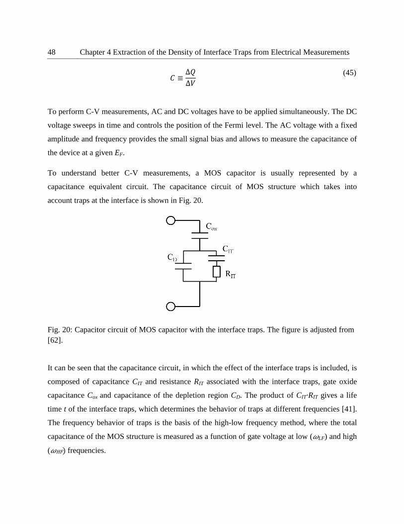
48 Chapter 4 Extraction of the Density of Interface Traps from Electrical Measurements
𝐶 ≡∆𝑄
∆𝑉
(45)
To perform C-V measurements, AC and DC voltages have to be applied simultaneously. The DC
voltage sweeps in time and controls the position of the Fermi level. The AC voltage with a fixed
amplitude and frequency provides the small signal bias and allows to measure the capacitance of
the device at a given EF.
To understand better C-V measurements, a MOS capacitor is usually represented by a
capacitance equivalent circuit. The capacitance circuit of MOS structure which takes into
account traps at the interface is shown in Fig. 20.
Fig. 20: Capacitor circuit of MOS capacitor with the interface traps. The figure is adjusted from
[62].
It can be seen that the capacitance circuit, in which the effect of the interface traps is included, is
composed of capacitance CIT and resistance RIT associated with the interface traps, gate oxide
capacitance Cox and capacitance of the depletion region CD. The product of CIT·RIT gives a life
time t of the interface traps, which determines the behavior of traps at different frequencies [41].
The frequency behavior of traps is the basis of the high-low frequency method, where the total
capacitance of the MOS structure is measured as a function of gate voltage at low (𝜔LF) and high
(𝜔HF) frequencies.
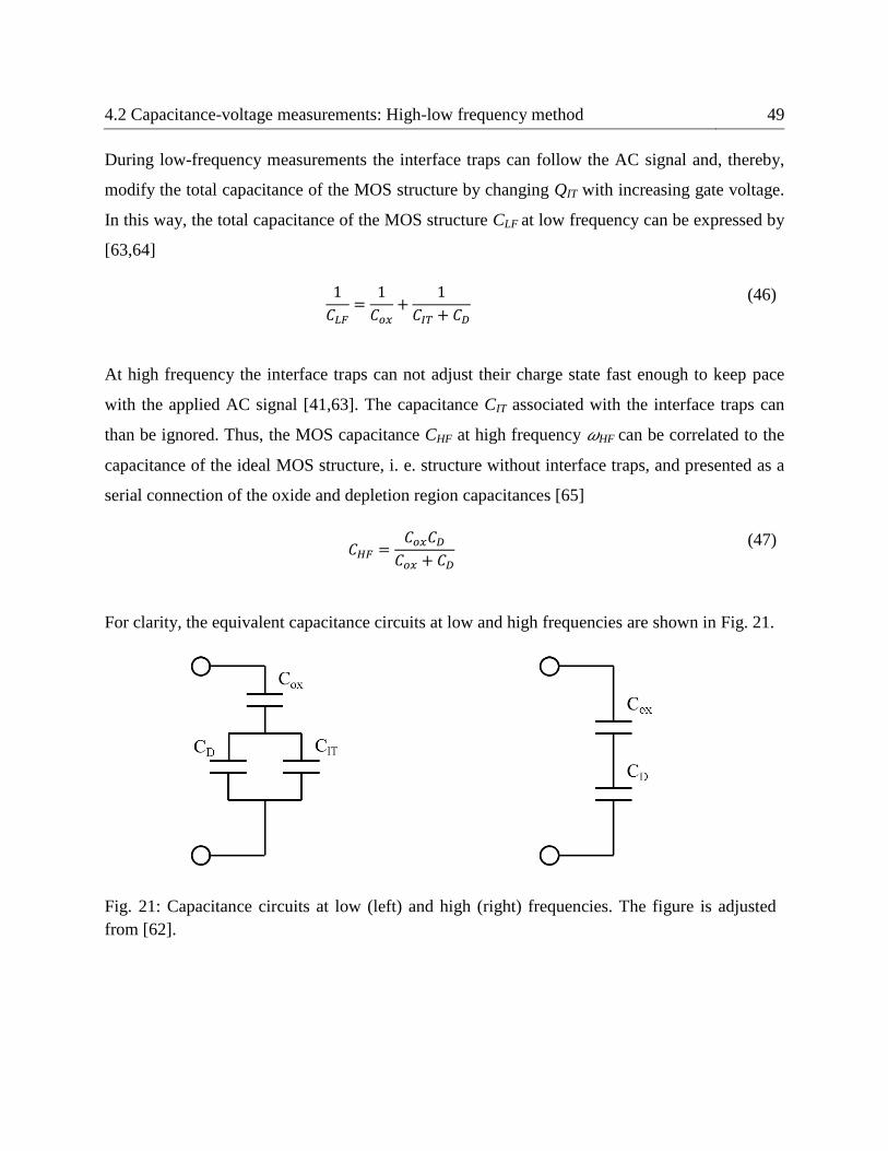
4.2 Capacitance-voltage measurements: High-low frequency method 49
During low-frequency measurements the interface traps can follow the AC signal and, thereby,
modify the total capacitance of the MOS structure by changing QIT with increasing gate voltage.
In this way, the total capacitance of the MOS structure CLF at low frequency can be expressed by
[63,64]
1
𝐶𝐿𝐹=1
𝐶𝑜𝑥+
1
𝐶𝐼𝑇 + 𝐶𝐷
(46)
At high frequency the interface traps can not adjust their charge state fast enough to keep pace
with the applied AC signal [41,63]. The capacitance CIT associated with the interface traps can
than be ignored. Thus, the MOS capacitance CHF at high frequency 𝜔HF can be correlated to the
capacitance of the ideal MOS structure, i. e. structure without interface traps, and presented as a
serial connection of the oxide and depletion region capacitances [65]
𝐶𝐻𝐹 =𝐶𝑜𝑥𝐶𝐷𝐶𝑜𝑥 + 𝐶𝐷
(47)
For clarity, the equivalent capacitance circuits at low and high frequencies are shown in Fig. 21.
Fig. 21: Capacitance circuits at low (left) and high (right) frequencies. The figure is adjusted
from [62].
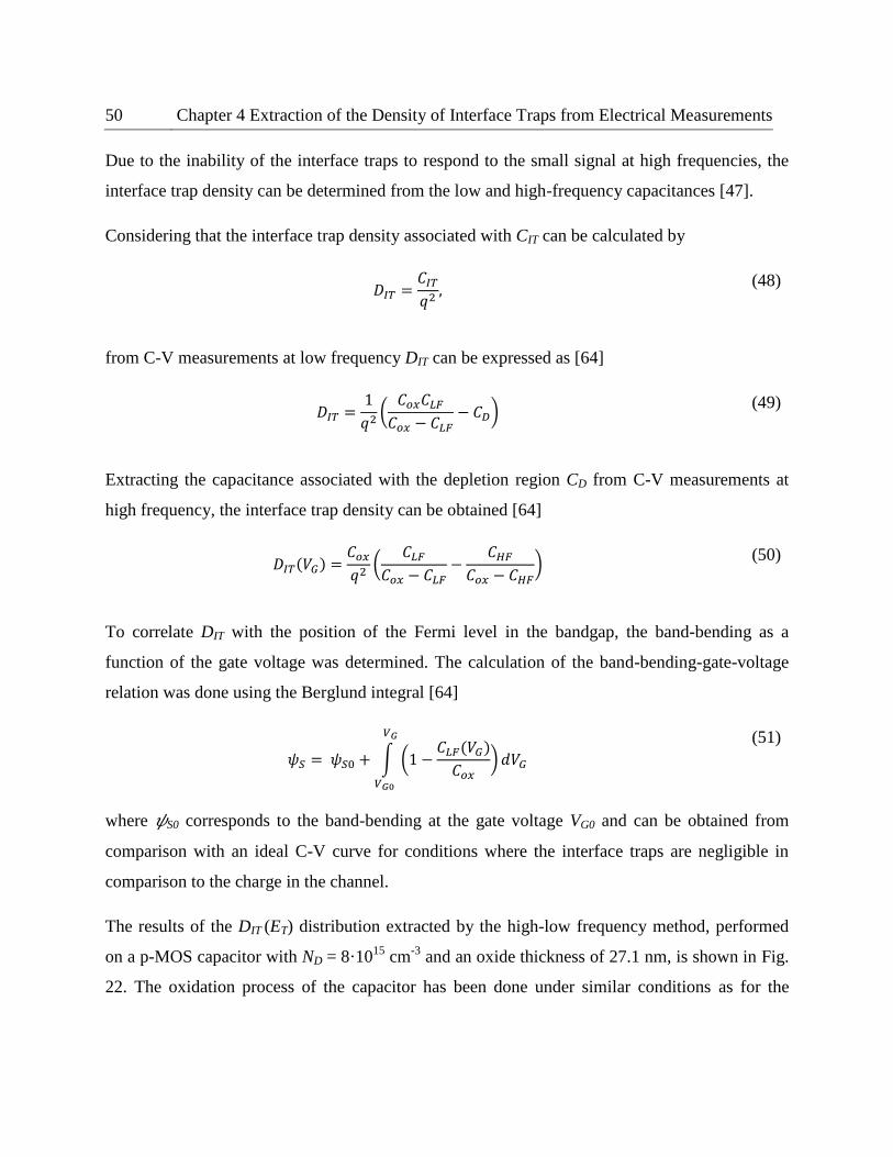
50 Chapter 4 Extraction of the Density of Interface Traps from Electrical Measurements
Due to the inability of the interface traps to respond to the small signal at high frequencies, the
interface trap density can be determined from the low and high-frequency capacitances [47].
Considering that the interface trap density associated with CIT can be calculated by
𝐷𝐼𝑇 =𝐶𝐼𝑇𝑞2,
(48)
from C-V measurements at low frequency DIT can be expressed as [64]
𝐷𝐼𝑇 =1
𝑞2(𝐶𝑜𝑥𝐶𝐿𝐹𝐶𝑜𝑥 − 𝐶𝐿𝐹
− 𝐶𝐷) (49)
Extracting the capacitance associated with the depletion region CD from C-V measurements at
high frequency, the interface trap density can be obtained [64]
𝐷𝐼𝑇(𝑉𝐺) =𝐶𝑜𝑥𝑞2(
𝐶𝐿𝐹𝐶𝑜𝑥 − 𝐶𝐿𝐹
−𝐶𝐻𝐹
𝐶𝑜𝑥 − 𝐶𝐻𝐹)
(50)
To correlate DIT with the position of the Fermi level in the bandgap, the band-bending as a
function of the gate voltage was determined. The calculation of the band-bending-gate-voltage
relation was done using the Berglund integral [64]
𝜓𝑆 = 𝜓𝑆0 + ∫ (1 −𝐶𝐿𝐹(𝑉𝐺)
𝐶𝑜𝑥)𝑑𝑉𝐺
𝑉𝐺
𝑉𝐺0
(51)
where 𝜓S0 corresponds to the band-bending at the gate voltage VG0 and can be obtained from
comparison with an ideal C-V curve for conditions where the interface traps are negligible in
comparison to the charge in the channel.
The results of the DIT (ET) distribution extracted by the high-low frequency method, performed
on a p-MOS capacitor with ND = 8·1015
cm-3
and an oxide thickness of 27.1 nm, is shown in Fig.
22. The oxidation process of the capacitor has been done under similar conditions as for the
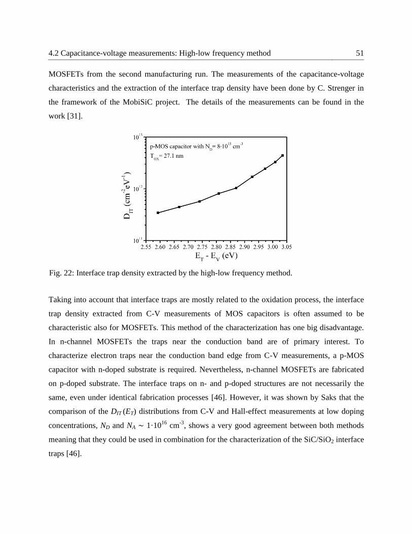
4.2 Capacitance-voltage measurements: High-low frequency method 51
MOSFETs from the second manufacturing run. The measurements of the capacitance-voltage
characteristics and the extraction of the interface trap density have been done by C. Strenger in
the framework of the MobiSiC project. The details of the measurements can be found in the
work [31].
Fig. 22: Interface trap density extracted by the high-low frequency method.
Taking into account that interface traps are mostly related to the oxidation process, the interface
trap density extracted from C-V measurements of MOS capacitors is often assumed to be
characteristic also for MOSFETs. This method of the characterization has one big disadvantage.
In n-channel MOSFETs the traps near the conduction band are of primary interest. To
characterize electron traps near the conduction band edge from C-V measurements, a p-MOS
capacitor with n-doped substrate is required. Nevertheless, n-channel MOSFETs are fabricated
on p-doped substrate. The interface traps on n- and p-doped structures are not necessarily the
same, even under identical fabrication processes [46]. However, it was shown by Saks that the
comparison of the DIT (ET) distributions from C-V and Hall-effect measurements at low doping
concentrations, ND and NA ~ 1·1016
cm-3
, shows a very good agreement between both methods
meaning that they could be used in combination for the characterization of the SiC/SiO2 interface
traps [46].
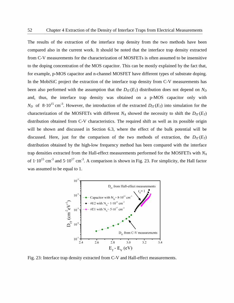
52 Chapter 4 Extraction of the Density of Interface Traps from Electrical Measurements
The results of the extraction of the interface trap density from the two methods have been
compared also in the current work. It should be noted that the interface trap density extracted
from C-V measurements for the characterization of MOSFETs is often assumed to be insensitive
to the doping concentration of the MOS capacitor. This can be mostly explained by the fact that,
for example, p-MOS capacitor and n-channel MOSFET have different types of substrate doping.
In the MobiSiC project the extraction of the interface trap density from C-V measurements has
been also performed with the assumption that the DIT (ET) distribution does not depend on ND
and, thus, the interface trap density was obtained on a p-MOS capacitor only with
ND of 8·1015
cm-3
. However, the introduction of the extracted DIT (ET) into simulation for the
characterization of the MOSFETs with different NA showed the necessity to shift the DIT (ET)
distribution obtained from C-V characteristics. The required shift as well as its possible origin
will be shown and discussed in Section 6.3, where the effect of the bulk potential will be
discussed. Here, just for the comparison of the two methods of extraction, the DIT (ET)
distribution obtained by the high-low frequency method has been compared with the interface
trap densities extracted from the Hall-effect measurements performed for the MOSFETs with NA
of 1·1015
cm-3
and 5·1017
cm-3
. A comparison is shown in Fig. 23. For simplicity, the Hall factor
was assumed to be equal to 1.
Fig. 23: Interface trap density extracted from C-V and Hall-effect measurements.
4.2 Capacitance-voltage measurements: High-low frequency method 53
At first sight it can be seen from the comparison that the interface trap density measured on an n-
doped MOS capacitor fits well to the DIT extracted from Hall-effect measurements performed for
MOSFETs with different Al concentrations. However, between the DIT distributions extracted
from C-V and Hall-effect measurements there is an uncovered part of the energetic distribution
of traps. The existence of this part can be explained by the limitations of the methods in the
determination of the energetic position of the traps, discussed in Section 3.4.2. This part in the
DIT (ET) distribution can be replaced, for example, using a linear interpolation. Nevertheless,
considering the non-uniform DIT distributions over the SiC bandgap, the existence of small peaks
instead of a linear distribution can not be excluded.

55
Chapter 5 Method of Hall Factor Calculation
Hall-effect measurements in combination with sheet resistivity measurements are well
established to determine sheet carrier density and mobility of charge carriers independently in
semiconductors and metals. However, from the combination of the measured values one obtains
an effective Hall mobility µH rather than the drift mobility µ of the majority charge carriers. The
ratio of the two is called Hall factor or scattering factor and needs to be known a-priori for an
accurate interpretation of Hall-effect measurements. For lower fields and non-degenerate
semiconductors, the Hall factor depends on the particular mechanisms by which the charge
carriers are scattered and this may depend in turn on material and measurement condition. For
bulk SiC, rH was determined experimentally and investigated theoretically [66,67,68]. For the
significantly more complicated situation in the channel of SiC MOSFETs, it is common practice
to assume a Hall factor equal to unity [52]. From the theory of Hall-effect measurements it is
known that rH approaches unity in strong magnetic fields B for which the condition µB >> 1 is
satisfied. For a magnetic field of B = 1 T, as an example, this means that the mobility should be
significantly higher than 10,000 cm2/Vs. In SiC MOSFETs, the drift mobility in the channel is
typically on the order of 10 to 100 cm2/Vs [45,52]. As a consequence, the assumption of rH = 1
may lead to a misinterpretation of Hall-effect measurements by up to some 10% which is
considerable for such devices.
In literature, various approaches have been presented to calculate transport properties and Hall
factors. They are typically based on Monte Carlo methods or solutions of the Boltzmann
transport equation taking the full band structure into account [67,69]. Despite being
computationally demanding, they still need comparison with experiments and cannot be easily

56 Chapter 5 Method of Hall Factor Calculation
applied to general conditions in macroscopic devices. In this work, a new method for the
calculation of Hall factors is presented. It is based on the fact that both Hall factor and mobility
depend on the mechanisms by which the charge carriers are actually scattered [VU1]. The links
between the various mobility components and the Hall factor are the respective relaxation
scattering times. A particular advantage of the method is that it can be easily applied for different
materials under different measurement conditions.
5.1 On the calculation of Hall factor for the characterization of electronic
devices
The Hall factor rH0 is defined as the ratio of the Hall mobility to drift mobility and can be
expressed in the relaxation scattering time approximation through certain mean values of
relaxation times:
𝑟𝐻0 =µ𝐻µ= < 𝜏2 >
< 𝜏 >2
(52)
Therein, the parameter τ denotes the relaxation time, i.e. the mean free flight time between
carrier collisions. In general, it will depend on the energy of the charge carriers. The squared
brackets denote an averaging over the energy of the charge carriers. The inverse of the relaxation
time 1/τ is the average number of scattering events per unit time. For many scattering processes,
the energy dependence of the relaxation time can be expressed as a simple power law:
𝜏 = 𝑎𝐸−𝑠 (53)
where a and s are constants whose values depend on the involved types of scattering
mechanisms. For example, for semiconductors with acoustic phonon or ionized impurity
scattering, τ is proportional to E -1/2
(s = 1/2) or to E
3/2 (s = -3/2), respectively [41].
As long as the relaxation time can be expressed in the form of a power law, the values of the
averages <τ> and <τ2> can be calculated analytically:
5.1 On the calculation of Hall factor for the characterization of electronic devices 57
< 𝜏 >=𝑎(𝑘𝑇)−𝑠 Г(
52 − s)
Г (52)
,
(54)
< 𝜏2 >=𝑎2(𝑘𝑇)−2𝑠Г(
52 − 2𝑠)
Г (52)
(55)
where Г(n) is the gamma function defined as:
Г(𝑛) ≡ ∫ 𝑥𝑛−1𝑒−𝑥𝑑𝑥
∞
0
(56)
In accordance with Eq. (52), it follows from the expressions above that the Hall factor becomes
rH0 = 1.18 for surface-phonon scattering and rH0 = 1.93 for ionized impurity scattering. It was
also suggested by Erginsoy that the relaxation time for scattering at neutral impurities is
independent of the energy of the charge carriers (s = 0) [70]. For such a mechanism dominating
at extremely low temperature or for heavily doped semiconductors, the Hall factor becomes
rH0 = 1. In summary, depending on the actual scattering mechanism, values of the Hall factor rH0
may vary between 1 and 1.93.
In a real electronic device, several charge scattering mechanisms are usually involved in parallel.
In order to calculate the Hall factor from Eq. (52), the values of <τ> and <τ2> have to be
determined for such conditions. This can be done by accounting these several scattering
mechanisms when averaging relaxation times over energy. As suggested by Iwata [68], the
various scattering mechanisms can be combined in the form:
< 𝜏 > =
∫𝑥3 2⁄ 𝑒−𝑥𝑑𝑥∑ 𝜏𝑖
−1𝑖
∞
0
∫ 𝑥3 2⁄ 𝑒−𝑥𝑑𝑥∞
0
(57)
58 Chapter 5 Method of Hall Factor Calculation
< 𝜏2 > =
∫𝑥3 2⁄ 𝑒−𝑥𝑑𝑥[∑ 𝜏𝑖
−1𝑖 ]2
∞
0
∫ 𝑥3 2⁄ 𝑒−𝑥𝑑𝑥∞
0
(58)
where x stands for ε/kBT with ε denoting the kinetic energy of an electron and the index i the
particular scattering mechanism.
To apply Eq. (57) and Eq. (58) to certain experimental conditions, the relaxation times for each
of the scattering mechanisms and their dependence on the energy of the charge carriers under
investigation have to be known. For example, for measurements in a MOS structure, only
scattering of the prevalent charge carriers in the inversion layers should be considered. A
peculiarity of Hall-effect measurements in MOSFETs is scattering at interface charges which is
largely negligible for measurements on bulk semiconductor samples. This difference in the
measurement conditions can manifest itself in different Hall-factor values. The new method for
the calculation of Hall factors presented in this work allows master the complexity of the
necessary calculations. As indicated above, it takes advantage of the interdependence of the
scattering time with mobility. In general, the electron mobility in a semiconductor can be
expressed as:
𝜇𝑛 = 𝑞 < 𝜏 >
𝑚𝑒∗ (59)
where <τ> is the mean relaxation time that may contain the contributions from several scattering
processes, and 𝑚𝑒∗ stands for the effective electron mass. It is further assumed that the scattering
events are independent of each other so that neither of the τi is affected by other scattering
process. The contributions of the individual scattering times τi to the global scattering time τ can
then be combined in the form:
1
𝜏=∑
1
𝜏𝑖.
𝑖
(60)
5.1 On the calculation of Hall factor for the characterization of electronic devices 59
Since the electron mobility is proportional to τ, Eq.(60) can be rewritten in terms of the mobility
components µi associated with the various scattering mechanisms
1
µ=∑
1
µ𝑖.
𝑖
(61)
From Eq. (59) it is seen that the relaxation time and electron mobility differ only by a constant
factor of 𝑞/𝑚𝑒∗ . Having the possibility to calculate specific mobility components µi, the
components of scattering time τi associated with these mechanisms can be easily found. If a
power-law dependence of the relaxation time on the electron energy can be assumed, the
unknown constant a in Eq. (53) can be calculated from Eq. (54) and Eq. (59). Given a, the
energy dependence of the relaxation time for ith scattering component can be derived as:
𝜏𝑖(𝐸) =𝜇𝑖𝑚𝑒
∗Г (52)𝐸
−𝑠𝑖
𝑞(𝑘𝐵𝑇)−𝑠𝑖Г(
52 − 𝑠𝑖)
(62)
It should be noted that these formulas are valid for non-degenerate semiconductors with a single-
valley spherical energy band. For multi-valley semiconductors, such as Si, SiC and Ge, the
expression for the Hall factor has to be modified. For this purpose, the Hall factor given by
Eq. (52) for the single-valley model is multiplied by a constant a0 that accounts for the anisotropy
of the effective electron mass. Thus, the Hall factor for the case of a multiple conduction valley
semiconductor can be expressed in the form [71]
𝑟𝐻 = 𝑟𝐻0𝑎0 (63)
where rH0 is the scattering factor given by Eq.(52) for single-valley semiconductors assuming
isotropic model, and a0 is known as the “Hall mass factor” or anisotropy factor of the Hall-effect.
The latter is given by [71]
60 Chapter 5 Method of Hall Factor Calculation
𝑎0 =3𝐾(𝐾 + 2)
(2𝐾 + 1)2
(64)
with K being the ratio of longitudinal and transverse effective masses of the electrons. For Si,
SiC and Ge, the Hall mass factor a0 takes values of 0.87, 0.98 and 0.785, respectively.
Using Eqs. (57-62), and assuming the concurrent action of different scattering mechanisms, the
Hall factor can be easily determined and corrected with the anisotropy model given in Eq.(63).
5.2 Hall factor in bulk silicon
To check the feasibility of the new method for the calculation of Hall factors, it was applied to
the calculation of the Hall factor in bulk silicon, the values of which was extensively investigated
in the literature. Specifically, the dependence of the Hall factor in n-type silicon at room
temperature on the doping concentration was investigated. For this purpose, simulations of
electronic transport in phosphorus-doped silicon samples were performed for the range of
phosphorus concentration from 1·1017
cm-3
to 2·1020
cm-3
. Given bulk silicon, it was assumed
that the mobility is determined by Coulomb scattering at ionized impurities and by bulk-phonon
scattering. To model the mobility component due to bulk-phonon scattering, a constant mobility
of µBP = 1417 cm2/Vs at T = 300 K was adopted from the work of Lombardi et al. [72]. The
mobility component due to charged impurity scattering was calculated using the Arora model as
implemented in TCAD Sentaurus and is described by [30]
𝜇𝐵 = 𝜇𝑚𝑖𝑛1 +𝜇𝑑
1 + (𝑁𝐷+
𝑁0)𝐴
∗
(65)
with 𝑁𝐷+ standing for the ionized donor concentration and µmin1, 𝜇d, N0 and A
* > 0 for some given
parameters of the model. To predict the dependence of the Hall factor on the dopant
concentration, an analysis of Eq. (65) was done. It is clear from the functional dependence that
5.2 Hall factor in bulk silicon 61
the doping-related component will strictly decrease with an increasing doping concentration.
This is shown also in Fig. 24. It can be interpreted as an increase of the number of scattering
centers in the bulk with an increasing dopant concentration, leading further to a monotonic
increase of Coulomb scattering.
Fig. 24: Bulk mobility as a function of phosphorus concentration [VU1].
Keeping in mind that the Hall factor is rH0 = 1.18 for the limiting case of exclusive phonon
scattering and rH0 = 1.93 for the exclusive case of ionized impurity scattering, one expects also
an increase of the Hall factor with doping concentration. On the other hand, several groups found
experimentally that the Hall factor in n-type silicon increases with donor concentrations but only
until a doping level of about 3·1018
cm-3
[73,74,75,76]. With a further increase of doping
concentration, the Hall factor decreases and, for doping concentrations exceeding 1020
cm-3
, the
Hall factor approaches the theoretical value of rH = 0.87 [75]. This value of rH results from
rH0 = 1 in Eq. (63) with the anisotropy of the electron mass in silicon taken into consideration. It
is important here to point out that a value of rH0 = 1 indicates that the semiconductor has already
become degenerate [77]. Vice versa, the reduction of the Hall factor can be taken as an indication
that the importance of scattering at charged impurities decreases at sufficiently high doping
62 Chapter 5 Method of Hall Factor Calculation
levels. The apparent contradiction between the Hall factor found experimentally and predicted by
the model can be reconciled by noting that the effect of the screening due to the presence of
majority charge carriers has not been accounted for. This kind of screening is expected at very
high doping levels at which doping acts not only as a source of Coulomb scattering at ionized
impurities but simultaneously reduces it due to the increase in the concentration of majority
carriers.
To account for the screening of ionized impurities by majority carriers, the model proposed
should be adapted accordingly. The suggested modification for the degenerate case is based on
an analogy between screened ionized impurities and neutral impurities. At sufficiently low
dopant concentration, the distances between the ionized impurities are sufficiently large so that
the free electrons can be considered to exist separately from them. As the impurity concentration
and with it the concentration of free electrons increases, electrons will spend on their paths more
and more time in the vicinity of ionized impurities. For very high dopant concentrations,
impurities will find themselves surrounded by alternating electrons which compensate their
charge. In terms of the power-law energy dependence of the relaxation times, the power index s
in Eq. (53) should change accordingly from the value of -3/2 typical for ionized impurity
scattering to the value of 0 that is valid for the scattering on the neutral centers. Evidence from
the measurements of Hall factors indicates that this decrease happens at a doping level exceeding
about 3·1018
cm-3
which corresponds closely to the Mott transition [78]. To include the effect in
our Hall-factor calculation, based on the reasoning above, the predicted dependence of the power
index s on doping concentration ND was modeled empirically in the following form:
𝑠 = 1.5 ·
(
1
1 + (3 · 1019
𝑁𝐷)1.2 − 1
)
(66)
A graphical representation of this relationship can be found in Fig. 25. In accordance with
Eq. (66), the power index s changes from -3/2 to 0 when dopant concentration grows from zero
5.2 Hall factor in bulk silicon 63
to infinity. At low dopant densities, when screening of impurities by electrons is negligible, s has
its minimum equal to -3/2. With increasing screening, the importance of Coulomb scattering will
decrease, which is reflected in the increase of the constant s. Finally, at high doping levels
around 2·1020
cm-3
, the scattering is similar to that at neutral impurities, which is reflected in the
tendency of s towards the value of 0.
Fig. 25: Dependence of the power index s for Coulomb scattering on dopant density including
screening [VU1].
Taking the mobility degradation due to phonon and Coulomb scattering in the phosphorus-doped
silicon bulk material and introducing the effect of screening at high doping levels discussed
above into account, the Hall factor in the bulk Si was calculated using the method presented in
Section 5.1 as a function of dopant concentrations. The results of this calculation are shown in
Fig. 26 in comparison with the measurements reported in the literature for Si [74].
In accordance with the predictions of the new method, the Hall factor in bulk silicon increases up
to a doping level of 4·1018
cm-3
. When the phosphorus concentration increases further, the
screening of the ionized impurities by the majority charge carriers sets in and leads to a
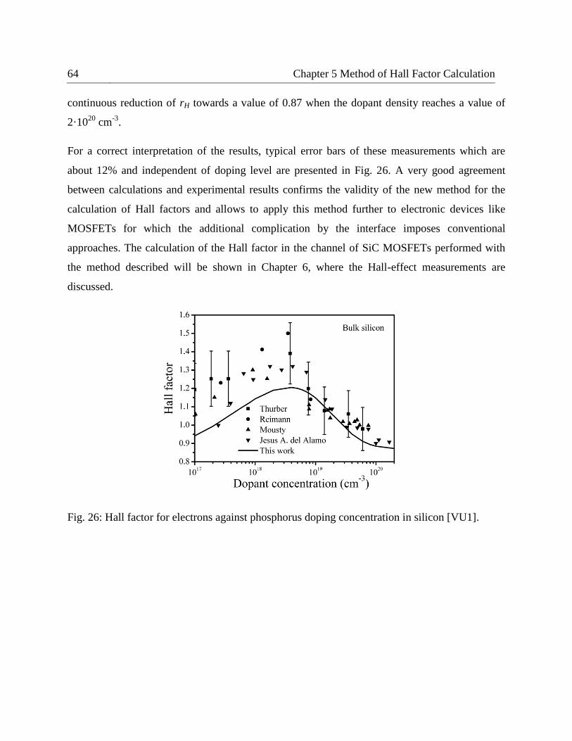
64 Chapter 5 Method of Hall Factor Calculation
continuous reduction of rH towards a value of 0.87 when the dopant density reaches a value of
2·1020
cm-3
.
For a correct interpretation of the results, typical error bars of these measurements which are
about 12% and independent of doping level are presented in Fig. 26. A very good agreement
between calculations and experimental results confirms the validity of the new method for the
calculation of Hall factors and allows to apply this method further to electronic devices like
MOSFETs for which the additional complication by the interface imposes conventional
approaches. The calculation of the Hall factor in the channel of SiC MOSFETs performed with
the method described will be shown in Chapter 6, where the Hall-effect measurements are
discussed.
Fig. 26: Hall factor for electrons against phosphorus doping concentration in silicon [VU1].
65
Chapter 6 Simulation Results and Discussions
To interpret the electrical characteristics of n-channel 4H-SiC MOSFETs determined by current-
voltage and Hall-effect measurements, numerical simulations have been performed. On the basis
of the MOSFET #E1 with a high background doping concentration, a simulation methodology
has been developed and applied further to study the effects of temperature and bulk potential
engineering upon transport properties in the channels of MOSFETs.
6.1 Simulation methodology: Current-voltage characteristics
To simulate the electrical characteristics of SiC MOSFETs, the interface traps which affect its
performance have to be properly described. Currently, in simulations it is commonly accepted to
focus on the traps which are related to the oxidation process of SiC, energetically located near
the conduction band of SiC and assumed to be acceptors. However, it can not be excluded that
other traps, which are specific to one or another fabrication process, can be introduced in
addition and have an impact on the performance of MOSFETs. There are a few research groups
who suggest that nitridation leads to a generation of donor impurity levels in the SiC bandgap
which affect the transport properties in the channel of SiC MOSFETs. Different measurement
techniques have been used already to investigate the behavior of nitrogen atoms introduced
during the nitridation. As an example, using x-ray photoelectron spectroscopy (XPS), Kosugi et
al. [79] showed that nitrogen atoms are not only embedded in the oxide layer but also remain
fixed at the SiC/SiO2 interface with an areal density of 1·1014
cm-2
even after removal of the
oxide layer by hydrogen-fluoride (HF) etching. To explain this result two assumptions have been
made. The first one is that nitrogen atoms can form strong chemical bonds at the interface. The
66 Chapter 6 Simulation Results and Discussions
second one is that nitrogen can be incorporated into the SiC and act as shallow donors. A similar
conclusion has been given by Fiorenza et al. in [80], where an effect of post-deposition annealing
(PDA) in N2O ambient was analyzed using scanning capacitance microscopy. By measuring the
carrier concentration in the n-type epitaxial layer of the MOS structure, it was demonstrated that
PDA in N2O ambient leads to the formation of a sharp concentration peak below the SiC/SiO2
interface. For example, an increase of the active doping concentration at the interface from
5·1015
cm-3
, which is the concentration of the n-type epitaxial layer, up to 5·1017
cm-3
has been
observed. The groups of Liu et al. [81] and Umeda et al. [82] have also proposed that some
nitrogen atoms can diffuse into a very thin layer of 1-2 nm of SiC forming an “interfacial counter
doping” during post-nitridation annealing. As a consequence, it can lead to the increase of the
carrier concentration in the channel and to a decrease of VTH in the MOSFETs. Nevertheless, the
current status of investigation of nitridation does not allow to assert explicitly how donor
impurities influence the electrical properties of MOSFETs. For example, the recent investigation
of Yoshioka reveals that because of the generation of donor traps near the SiC conduction band
the channel mobility can increase if NO annealing is performed at a certain temperature [83].
It can be seen that the behaviour of nitrogen atoms introduced during nitridation as well as its
role are very complex and still not fully understood. However, it seems that there is a common
agreement that nitridation leads to the incorporation of donor impurities close to the conduction
band of SiC. The same conclusion has been drawn in the current work analyzing the
measurements with Sentaurus Device.
In this thesis, one of the main tasks for numerical simulation is to explain the physical reasons
for the low performance of MOS transistors based on 4H-SiC with a gate oxide fabricated by
thermal oxidation in N2O atmosphere. For this purpose, numerical simulations with Sentaurus
Device have been performed and analyzed step by step. First, for reference, current-voltage
characteristics of n-channel transistors were calculated using the default simulation model that
assumes an ideal interface between the gate oxide and the 4H-SiC semiconductor. The results of
such simulations for the SiC MOSFET #E1 at a source-drain voltage of 0.1 V is shown in Fig. 27
in comparison with the results of the measurements.
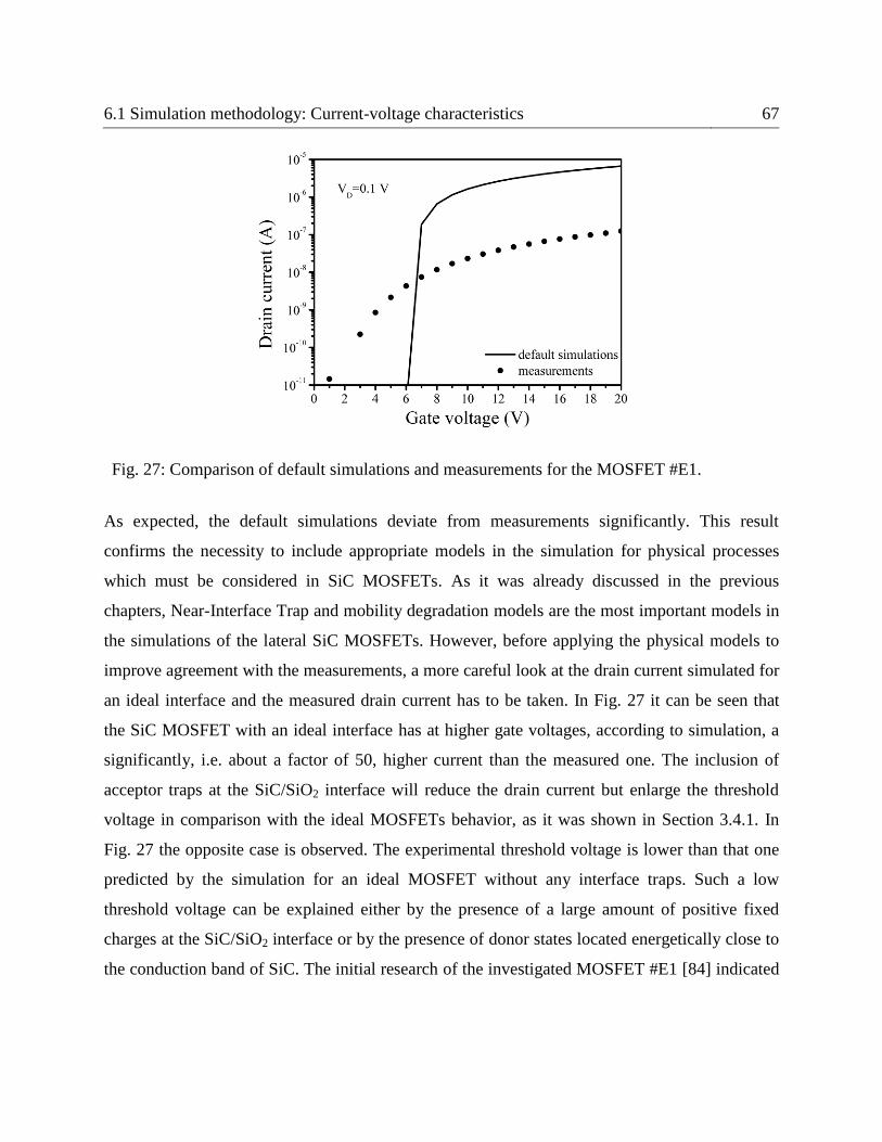
6.1 Simulation methodology: Current-voltage characteristics 67
Fig. 27: Comparison of default simulations and measurements for the MOSFET #E1.
As expected, the default simulations deviate from measurements significantly. This result
confirms the necessity to include appropriate models in the simulation for physical processes
which must be considered in SiC MOSFETs. As it was already discussed in the previous
chapters, Near-Interface Trap and mobility degradation models are the most important models in
the simulations of the lateral SiC MOSFETs. However, before applying the physical models to
improve agreement with the measurements, a more careful look at the drain current simulated for
an ideal interface and the measured drain current has to be taken. In Fig. 27 it can be seen that
the SiC MOSFET with an ideal interface has at higher gate voltages, according to simulation, a
significantly, i.e. about a factor of 50, higher current than the measured one. The inclusion of
acceptor traps at the SiC/SiO2 interface will reduce the drain current but enlarge the threshold
voltage in comparison with the ideal MOSFETs behavior, as it was shown in Section 3.4.1. In
Fig. 27 the opposite case is observed. The experimental threshold voltage is lower than that one
predicted by the simulation for an ideal MOSFET without any interface traps. Such a low
threshold voltage can be explained either by the presence of a large amount of positive fixed
charges at the SiC/SiO2 interface or by the presence of donor states located energetically close to
the conduction band of SiC. The initial research of the investigated MOSFET #E1 [84] indicated
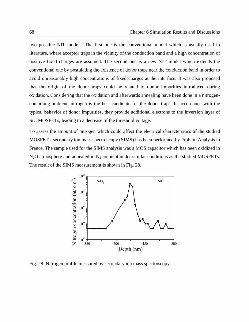
68 Chapter 6 Simulation Results and Discussions
two possible NIT models. The first one is the conventional model which is usually used in
literature, where acceptor traps in the vicinity of the conduction band and a high concentration of
positive fixed charges are assumed. The second one is a new NIT model which extends the
conventional one by postulating the existence of donor traps near the conduction band in order to
avoid unreasonably high concentrations of fixed charges at the interface. It was also proposed
that the origin of the donor traps could be related to donor impurities introduced during
oxidation. Considering that the oxidation and afterwards annealing have been done in a nitrogen-
containing ambient, nitrogen is the best candidate for the donor traps. In accordance with the
typical behavior of donor impurities, they provide additional electrons to the inversion layer of
SiC MOSFETs, leading to a decrease of the threshold voltage.
To assess the amount of nitrogen which could affect the electrical characteristics of the studied
MOSFETs, secondary ion mass spectroscopy (SIMS) has been performed by Probion Analysis in
France. The sample used for the SIMS analysis was a MOS capacitor which has been oxidized in
N2O atmosphere and annealed in N2 ambient under similar conditions as the studied MOSFETs.
The result of the SIMS measurement is shown in Fig. 28.
Fig. 28: Nitrogen profile measured by secondary ion mass spectroscopy.
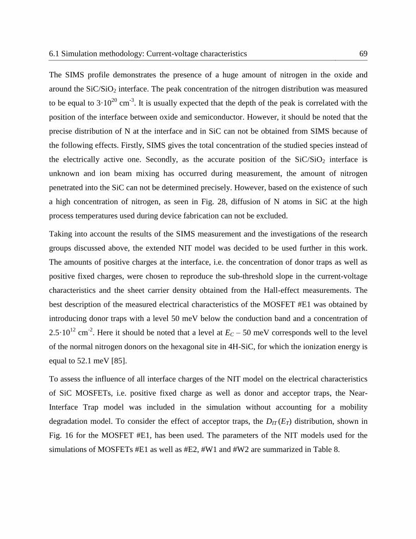
6.1 Simulation methodology: Current-voltage characteristics 69
The SIMS profile demonstrates the presence of a huge amount of nitrogen in the oxide and
around the SiC/SiO2 interface. The peak concentration of the nitrogen distribution was measured
to be equal to 3·1020
cm-3
. It is usually expected that the depth of the peak is correlated with the
position of the interface between oxide and semiconductor. However, it should be noted that the
precise distribution of N at the interface and in SiC can not be obtained from SIMS because of
the following effects. Firstly, SIMS gives the total concentration of the studied species instead of
the electrically active one. Secondly, as the accurate position of the SiC/SiO2 interface is
unknown and ion beam mixing has occurred during measurement, the amount of nitrogen
penetrated into the SiC can not be determined precisely. However, based on the existence of such
a high concentration of nitrogen, as seen in Fig. 28, diffusion of N atoms in SiC at the high
process temperatures used during device fabrication can not be excluded.
Taking into account the results of the SIMS measurement and the investigations of the research
groups discussed above, the extended NIT model was decided to be used further in this work.
The amounts of positive charges at the interface, i.e. the concentration of donor traps as well as
positive fixed charges, were chosen to reproduce the sub-threshold slope in the current-voltage
characteristics and the sheet carrier density obtained from the Hall-effect measurements. The
best description of the measured electrical characteristics of the MOSFET #E1 was obtained by
introducing donor traps with a level 50 meV below the conduction band and a concentration of
2.5·1012
cm-2
. Here it should be noted that a level at EC – 50 meV corresponds well to the level
of the normal nitrogen donors on the hexagonal site in 4H-SiC, for which the ionization energy is
equal to 52.1 meV [85].
To assess the influence of all interface charges of the NIT model on the electrical characteristics
of SiC MOSFETs, i.e. positive fixed charge as well as donor and acceptor traps, the Near-
Interface Trap model was included in the simulation without accounting for a mobility
degradation model. To consider the effect of acceptor traps, the DIT (ET) distribution, shown in
Fig. 16 for the MOSFET #E1, has been used. The parameters of the NIT models used for the
simulations of MOSFETs #E1 as well as #E2, #W1 and #W2 are summarized in Table 8.
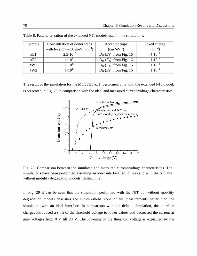
70 Chapter 6 Simulation Results and Discussions
Table 8. Parameterization of the extended NIT models used in the simulations
Sample Concentration of donor traps
with level EC – 50 meV (cm-2
)
Acceptor traps
(cm-2
eV-1
)
Fixed charge
(cm-2
)
#E1 2.5·1012
DIT (ET) from Fig. 16 4·1011
#E2 1·1011
DIT (ET) from Fig. 16 1·1011
#W1 1·1011
DIT (ET) from Fig. 16 1·1011
#W2 1·1011
DIT (ET) from Fig. 16 1·1011
The result of the simulation for the MOSFET #E1, performed only with the extended NIT model,
is presented in Fig. 29 in comparison with the ideal and measured current-voltage characteristics.
Fig. 29: Comparison between the simulated and measured current-voltage characteristics. The
simulations have been performed assuming an ideal interface (solid line) and with the NIT but
without mobility degradation models (dashed line).
In Fig. 29 it can be seen that the simulation performed with the NIT but without mobility
degradation models describes the sub-threshold slope of the measurements better than the
simulation with an ideal interface. In comparison with the default simulation, the interface
charges introduced a shift of the threshold voltage to lower values and decreased the current at
gate voltages from 8 V till 20 V. The lowering of the threshold voltage is explained by the
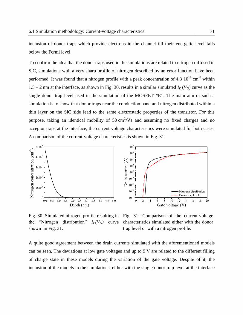
6.1 Simulation methodology: Current-voltage characteristics 71
inclusion of donor traps which provide electrons in the channel till their energetic level falls
below the Fermi level.
To confirm the idea that the donor traps used in the simulations are related to nitrogen diffused in
SiC, simulations with a very sharp profile of nitrogen described by an error function have been
performed. It was found that a nitrogen profile with a peak concentration of 4.8·1019
cm-3
within
1.5 – 2 nm at the interface, as shown in Fig. 30, results in a similar simulated ID (VG) curve as the
single donor trap level used in the simulation of the MOSFET #E1. The main aim of such a
simulation is to show that donor traps near the conduction band and nitrogen distributed within a
thin layer on the SiC side lead to the same electrostatic properties of the transistor. For this
purpose, taking an identical mobility of 50 cm2/Vs and assuming no fixed charges and no
acceptor traps at the interface, the current-voltage characteristics were simulated for both cases.
A comparison of the current-voltage characteristics is shown in Fig. 31.
Fig. 30: Simulated nitrogen profile resulting in
the “Nitrogen distribution” ID(VG) curve
shown in Fig. 31.
Fig. 31: Comparison of the current-voltage
characteristics simulated either with the donor
trap level or with a nitrogen profile.
A quite good agreement between the drain currents simulated with the aforementioned models
can be seen. The deviations at low gate voltages and up to 9 V are related to the different filling
of charge state in these models during the variation of the gate voltage. Despite of it, the
inclusion of the models in the simulations, either with the single donor trap level at the interface
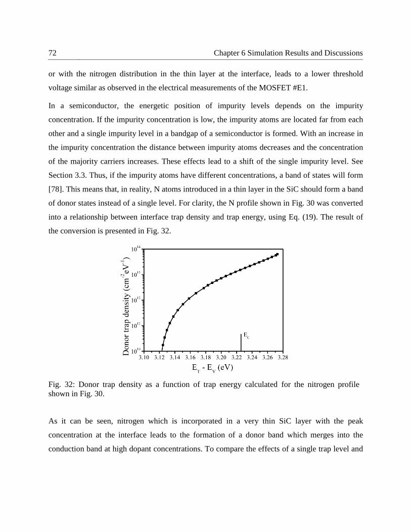
72 Chapter 6 Simulation Results and Discussions
or with the nitrogen distribution in the thin layer at the interface, leads to a lower threshold
voltage similar as observed in the electrical measurements of the MOSFET #E1.
In a semiconductor, the energetic position of impurity levels depends on the impurity
concentration. If the impurity concentration is low, the impurity atoms are located far from each
other and a single impurity level in a bandgap of a semiconductor is formed. With an increase in
the impurity concentration the distance between impurity atoms decreases and the concentration
of the majority carriers increases. These effects lead to a shift of the single impurity level. See
Section 3.3. Thus, if the impurity atoms have different concentrations, a band of states will form
[78]. This means that, in reality, N atoms introduced in a thin layer in the SiC should form a band
of donor states instead of a single level. For clarity, the N profile shown in Fig. 30 was converted
into a relationship between interface trap density and trap energy, using Eq. (19). The result of
the conversion is presented in Fig. 32.
Fig. 32: Donor trap density as a function of trap energy calculated for the nitrogen profile
shown in Fig. 30.
As it can be seen, nitrogen which is incorporated in a very thin SiC layer with the peak
concentration at the interface leads to the formation of a donor band which merges into the
conduction band at high dopant concentrations. To compare the effects of a single trap level and
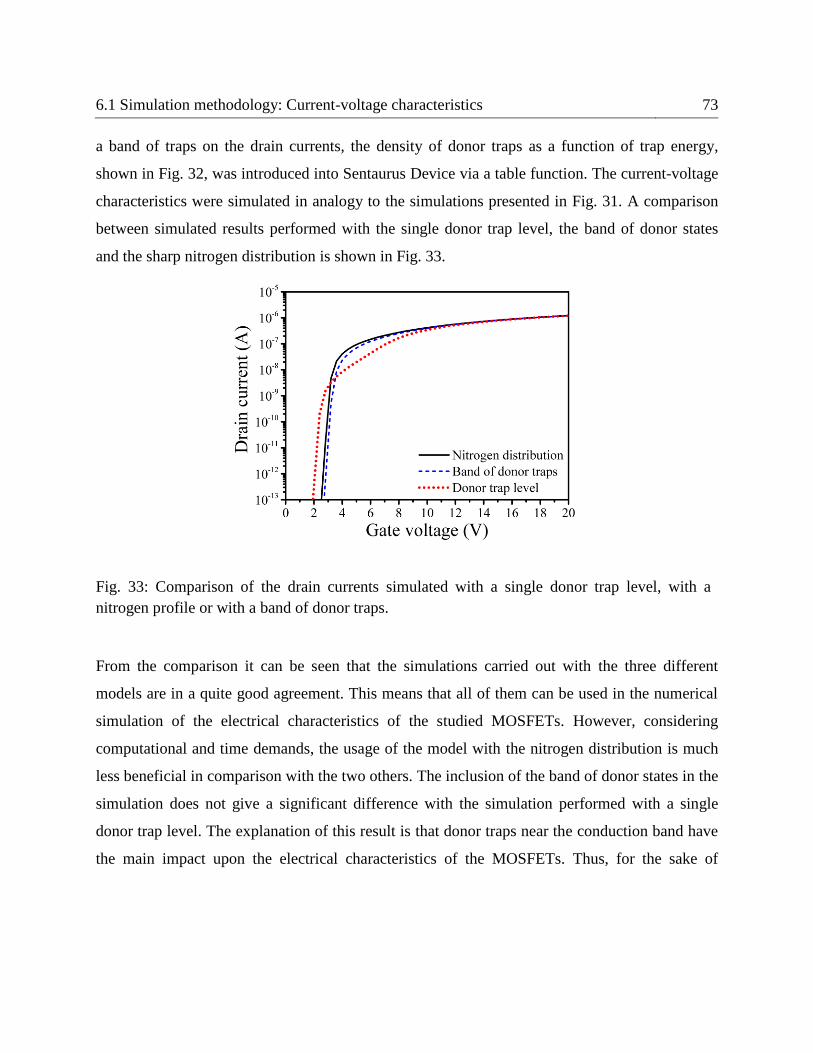
6.1 Simulation methodology: Current-voltage characteristics 73
a band of traps on the drain currents, the density of donor traps as a function of trap energy,
shown in Fig. 32, was introduced into Sentaurus Device via a table function. The current-voltage
characteristics were simulated in analogy to the simulations presented in Fig. 31. A comparison
between simulated results performed with the single donor trap level, the band of donor states
and the sharp nitrogen distribution is shown in Fig. 33.
Fig. 33: Comparison of the drain currents simulated with a single donor trap level, with a
nitrogen profile or with a band of donor traps.
From the comparison it can be seen that the simulations carried out with the three different
models are in a quite good agreement. This means that all of them can be used in the numerical
simulation of the electrical characteristics of the studied MOSFETs. However, considering
computational and time demands, the usage of the model with the nitrogen distribution is much
less beneficial in comparison with the two others. The inclusion of the band of donor states in the
simulation does not give a significant difference with the simulation performed with a single
donor trap level. The explanation of this result is that donor traps near the conduction band have
the main impact upon the electrical characteristics of the MOSFETs. Thus, for the sake of
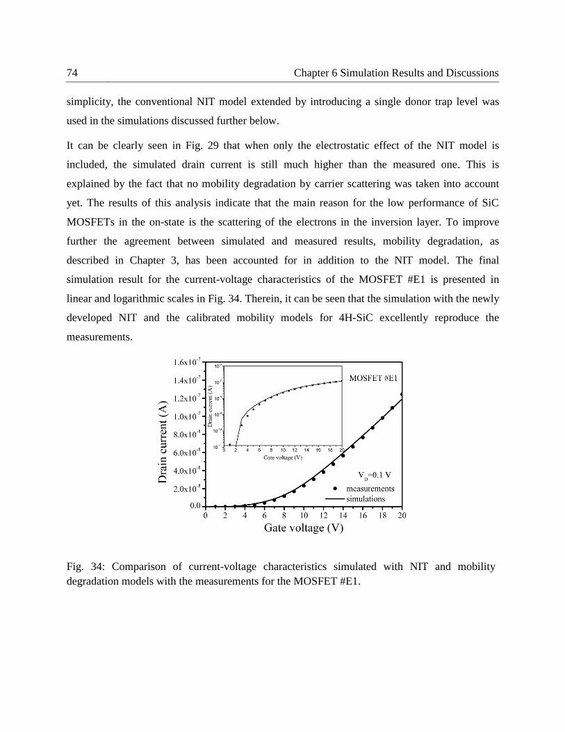
74 Chapter 6 Simulation Results and Discussions
simplicity, the conventional NIT model extended by introducing a single donor trap level was
used in the simulations discussed further below.
It can be clearly seen in Fig. 29 that when only the electrostatic effect of the NIT model is
included, the simulated drain current is still much higher than the measured one. This is
explained by the fact that no mobility degradation by carrier scattering was taken into account
yet. The results of this analysis indicate that the main reason for the low performance of SiC
MOSFETs in the on-state is the scattering of the electrons in the inversion layer. To improve
further the agreement between simulated and measured results, mobility degradation, as
described in Chapter 3, has been accounted for in addition to the NIT model. The final
simulation result for the current-voltage characteristics of the MOSFET #E1 is presented in
linear and logarithmic scales in Fig. 34. Therein, it can be seen that the simulation with the newly
developed NIT and the calibrated mobility models for 4H-SiC excellently reproduce the
measurements.
Fig. 34: Comparison of current-voltage characteristics simulated with NIT and mobility
degradation models with the measurements for the MOSFET #E1.
6.2 Simulation methodology: Hall-effect measurements 75
Simulations of the current-voltage characteristics for the MOSFETs #E2, #W1 and #W2 from the
second manufacturing run, results of which will be shown in Section 6.3, have been performed in
analogy to the simulations of the MOSFET #E1. Here it should be noted that the amount of
positive charge needed to bring the simulated and measured threshold voltage for the MOSFETs
#E2, #W1, #W2 into agreement was significantly less in comparison to the amount for the
MOSFET #E1. The required concentration of donor traps with the same level of EC – 50 meV
was only 1·1011
cm-2
. Additionally, the reduction of the concentration of positive fixed charges
was also found for the MOSFETs #E2, #W1 and #W2 as mentioned in Section 3.4.2.
The decrease of the concentration of the donor traps in the samples from the second
manufacturing run can be partially explained by a shorter nitridation time [86]. However, the
total reduction of the positive charges, i.e. the concentrations of donor traps and fixed charges,
can be related mainly to a replacement of the inner tube of the oxidation furnace before the
second manufacturing run [87]. The necessity of the replacement was caused by the
contamination of the tube with a high concentration of positive ions as observed experimentally.
This means that chemical elements as phosphorus, sodium and other donor impurities possibly
present in the first run could have an impact on the electrical characteristics of MOSFET #E1.
6.2 Simulation methodology: Hall-effect measurements
The correct determination of the channel mobility is one of the main challenges in the
characterization of SiC MOSFETs. One of the easiest methods to obtain the channel mobility is
to extract it from current-voltage characteristics by calculation of field-effect 𝜇FE or effective
𝜇EFF mobilities [46]:
𝜇𝐹𝐸 =𝐿
𝑊𝑉𝐷𝐶𝑜𝑥(𝜕𝐼𝐷𝜕𝑉𝐺
) (67)
76 Chapter 6 Simulation Results and Discussions
𝜇𝐸𝐹𝐹 =𝐿
𝑊𝑉𝐷
𝐼𝐷𝐶𝑜𝑥(𝑉𝐺 − 𝑉𝑇𝐻)
(68)
The calculation of field-effect and effective mobilities is widely used and well established in Si
MOSFETs. In SiC MOSFETs it can be used also but only for a qualitative analysis [46]. The
existence of a high trap density at the SiC/SiO2 interface in comparison to the Si/SiO2 interface
introduces inaccuracies in the determination of the mobility in SiC MOSFETs from their current-
voltage characteristics. The main inaccuracy in the calculation is related to the fact that Eq. (67)
and Eq. (68) is valid if the sheet carrier density in the inversion channel ninv is approximately
equal to the total number of electrons ntotal = Cox(VG – VTH)/q which can be theoretically induced
at the interface by applying a certain gate voltage [46]. However, due to the high density of traps
at the SiC/SiO2 interface, this approach is not suitable for SiC MOSFETs and leads to an
underestimation of the mobility in the channel. To perform precise studies of the transport
properties in SiC MOSFETs and to analyze the transport mechanisms in the channel of the
devices, a more accurate method of characterization is needed. One of the methods which allows
to determine the sheet carrier density as well as the mobility in the inversion layer independently
is based on Hall-effect measurements. However, as it was already discussed in Chapter 5, the
major disadvantage of the Hall-effect measurements is the unknown Hall factor. In case of SiC
MOSFETs, the uncertainty related to the Hall factor is even more critical than in Si MOSFETs
because of the dominance of Coulomb scattering in the inversion channel. The higher the amount
of interface traps, the higher the Coulomb scattering. Considering that in theory the Hall factor
calculated for the exclusive case of Coulomb scattering has a maximum value of 1.93 [41], a
higher value of the Hall factor will be expected in the inversion channel of SiC MOSFETs than
of Si ones. This means, to determine the sheet carrier density and the mobility in the channel of
SiC MOSFETs from Hall-effect measurements accurately, one has to calculate the Hall factor in
the channel of the transistor.
In order to calculate the Hall factor for the electrons in the channel of SiC MOSFETs using the
scattering relaxation time approximation discussed in Chapter 5, the values of <τ> and <τ2> at
6.2 Simulation methodology: Hall-effect measurements 77
the SiC/SiO2 interface have to be determined. Based on the method of the Hall factor calculation,
where the interdependence between scattering relaxation time and mobility is considered, the
Hall factor and the mobility in the channel of MOSFETs are determined by the same scattering
mechanisms. It is well known that the main limiting mechanisms of the total mobility in the
inversion layer of SiC MOSFETs are Coulomb scattering at ionized impurities in the bulk and at
the interface charges as well as surface-roughness, surface-phonon and bulk-phonon scattering.
Taking into account scattering mechanisms which are specific for the channel of MOSFETs and
using Eq. (57) and Eq. (58), the average scattering relaxation times can be given [68]:
< 𝜏 > =
∫𝑥3 2⁄ 𝑒−𝑥𝑑𝑥
𝜏𝐼𝑀𝑃−1 (𝑥)+𝜏𝐶
−1(𝑥) + 𝜏𝑆𝑅−1(𝑥) + 𝜏𝑆𝑃
−1(𝑥) + 𝜏𝐵𝑃−1(𝑥)
∞
0
∫ 𝑥3 2⁄ 𝑒−𝑥𝑑𝑥∞
0
(69)
< 𝜏2 > =
∫𝑥3 2⁄ 𝑒−𝑥𝑑𝑥
[𝜏𝐼𝑀𝑃−1 (𝑥) + 𝜏𝐶
−1(𝑥) + 𝜏𝑆𝑅−1(𝑥) + 𝜏𝑆𝑃
−1(𝑥) + 𝜏𝐵𝑃−1(𝑥)]2
∞
0
∫ 𝑥3 2⁄ 𝑒−𝑥𝑑𝑥∞
0
(70)
Therein, the scattering relaxation time components τIMP and τC are associated with Coulomb
scattering at ionized impurities in the bulk and at the interface charges, τSR, τSP and τBP with
surface-roughness, surface-phonon and bulk-phonon scattering, respectively.
Applying the method of Hall factor calculation, the scattering relaxation time components in
Eq. (69) and Eq. (70) can be easily determined from the respective mobility components. In the
current work, the calculation of the mobility components is based on the TCAD simulation of the
current-voltage characteristics, which reproduce the measured one. However, it should be noted
here that the implementation of the mobility degradation models in Sentaurus Device allows only
to assess the total channel mobility via its influence on the drain current and not the individual
mobility components themselves. To evaluate the contributions of the mobility components to
the total channel mobility, a method of small variations was used in the simulations. This method
78 Chapter 6 Simulation Results and Discussions
is based on applying a small variation to one of the mobility components via its accessible
parameters and in calculating its value from the resulting variation of the channel current.
To present clearly the idea of the method of small variations, the method is illustrated by the
following example. It is known that for small drain voltages, i.e. VD ≤ 0.10 V, the average
mobility of the electrons in the inversion layer can be derived from the current-voltage
characteristics of the device [46]:
If the total mobility varies from the initial value µ to a new value µ' that is close to µ, the
following expression can be obtained from Eq. (71):
𝜇′
𝜇=𝐼𝐷′
𝐼𝐷
(72)
Therein, ID' is a recalculated drain current that reflects the change in mobility from µ to µ'.
The channel mobility determined by Eq. (71) from the current-voltage characteristics can be also
given as a sum of the mobility components using Matthiessen’s rule in Eq. (23). Based on it one
of the inverse mobility components 𝜇𝑖−1 can be varied by the multiplication with a value δ=1+Δ,
where Δ is much smaller than unity. Then, applying some mathematical transformations to
Eq. (23), the following expression for the new value of µ' can be obtained:
1
𝜇′=1
𝜇+𝛥
𝜇𝑖
(73)
Varying each mobility component used in the TCAD simulation of the current-voltage
characteristics, the mobility component µi associated with the particular scattering mechanisms
in the channel of SiC MOSFETs can be derived by:
𝜇 =𝐼𝐷𝐿
𝑞𝑊𝑉𝐷𝑛𝑖𝑛𝑣
(71)
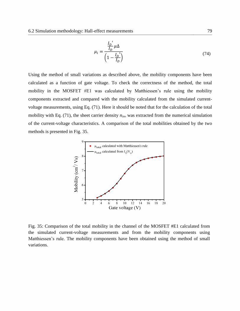
6.2 Simulation methodology: Hall-effect measurements 79
𝜇𝑖 =
𝐼𝐷′
𝐼𝐷𝜇∆
(1 −𝐼𝐷′
𝐼𝐷)
(74)
Using the method of small variations as described above, the mobility components have been
calculated as a function of gate voltage. To check the correctness of the method, the total
mobility in the MOSFET #E1 was calculated by Matthiessen’s rule using the mobility
components extracted and compared with the mobility calculated from the simulated current-
voltage measurements, using Eq. (71). Here it should be noted that for the calculation of the total
mobility with Eq. (71), the sheet carrier density ninv was extracted from the numerical simulation
of the current-voltage characteristics. A comparison of the total mobilities obtained by the two
methods is presented in Fig. 35.
Fig. 35: Comparison of the total mobility in the channel of the MOSFET #E1 calculated from
the simulated current-voltage measurements and from the mobility components using
Matthiessen’s rule. The mobility components have been obtained using the method of small
variations.
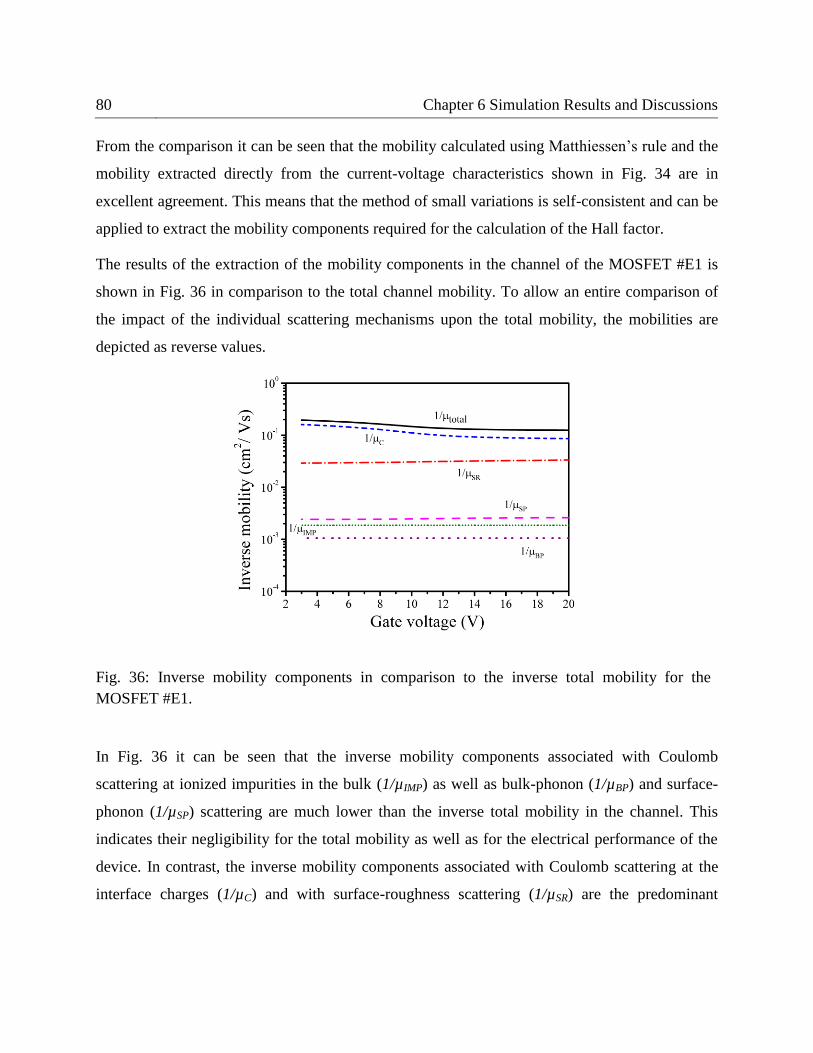
80 Chapter 6 Simulation Results and Discussions
From the comparison it can be seen that the mobility calculated using Matthiessen’s rule and the
mobility extracted directly from the current-voltage characteristics shown in Fig. 34 are in
excellent agreement. This means that the method of small variations is self-consistent and can be
applied to extract the mobility components required for the calculation of the Hall factor.
The results of the extraction of the mobility components in the channel of the MOSFET #E1 is
shown in Fig. 36 in comparison to the total channel mobility. To allow an entire comparison of
the impact of the individual scattering mechanisms upon the total mobility, the mobilities are
depicted as reverse values.
Fig. 36: Inverse mobility components in comparison to the inverse total mobility for the
MOSFET #E1.
In Fig. 36 it can be seen that the inverse mobility components associated with Coulomb
scattering at ionized impurities in the bulk (1/µIMP) as well as bulk-phonon (1/µBP) and surface-
phonon (1/µSP) scattering are much lower than the inverse total mobility in the channel. This
indicates their negligibility for the total mobility as well as for the electrical performance of the
device. In contrast, the inverse mobility components associated with Coulomb scattering at the
interface charges (1/µC) and with surface-roughness scattering (1/µSR) are the predominant
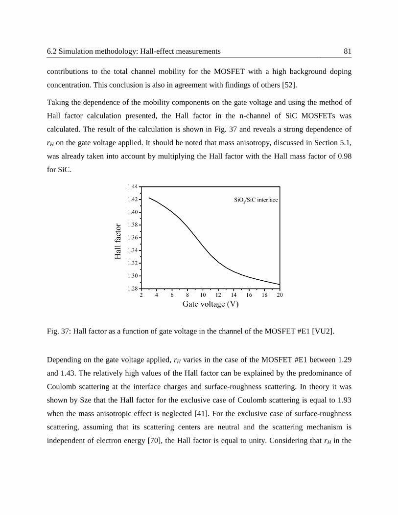
6.2 Simulation methodology: Hall-effect measurements 81
contributions to the total channel mobility for the MOSFET with a high background doping
concentration. This conclusion is also in agreement with findings of others [52].
Taking the dependence of the mobility components on the gate voltage and using the method of
Hall factor calculation presented, the Hall factor in the n-channel of SiC MOSFETs was
calculated. The result of the calculation is shown in Fig. 37 and reveals a strong dependence of
rH on the gate voltage applied. It should be noted that mass anisotropy, discussed in Section 5.1,
was already taken into account by multiplying the Hall factor with the Hall mass factor of 0.98
for SiC.
Fig. 37: Hall factor as a function of gate voltage in the channel of the MOSFET #E1 [VU2].
Depending on the gate voltage applied, rH varies in the case of the MOSFET #E1 between 1.29
and 1.43. The relatively high values of the Hall factor can be explained by the predominance of
Coulomb scattering at the interface charges and surface-roughness scattering. In theory it was
shown by Sze that the Hall factor for the exclusive case of Coulomb scattering is equal to 1.93
when the mass anisotropic effect is neglected [41]. For the exclusive case of surface-roughness
scattering, assuming that its scattering centers are neutral and the scattering mechanism is
independent of electron energy [70], the Hall factor is equal to unity. Considering that rH in the
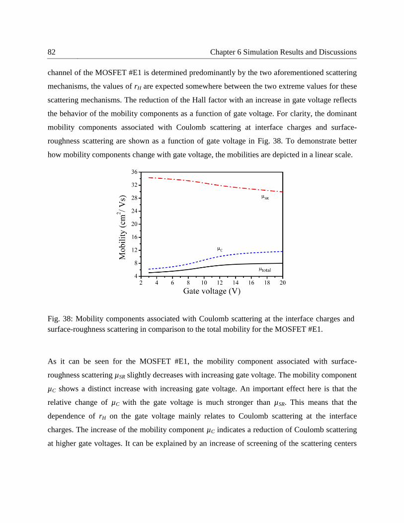
82 Chapter 6 Simulation Results and Discussions
channel of the MOSFET #E1 is determined predominantly by the two aforementioned scattering
mechanisms, the values of rH are expected somewhere between the two extreme values for these
scattering mechanisms. The reduction of the Hall factor with an increase in gate voltage reflects
the behavior of the mobility components as a function of gate voltage. For clarity, the dominant
mobility components associated with Coulomb scattering at interface charges and surface-
roughness scattering are shown as a function of gate voltage in Fig. 38. To demonstrate better
how mobility components change with gate voltage, the mobilities are depicted in a linear scale.
Fig. 38: Mobility components associated with Coulomb scattering at the interface charges and
surface-roughness scattering in comparison to the total mobility for the MOSFET #E1.
As it can be seen for the MOSFET #E1, the mobility component associated with surface-
roughness scattering µSR slightly decreases with increasing gate voltage. The mobility component
µC shows a distinct increase with increasing gate voltage. An important effect here is that the
relative change of µC with the gate voltage is much stronger than µSR. This means that the
dependence of rH on the gate voltage mainly relates to Coulomb scattering at the interface
charges. The increase of the mobility component µC indicates a reduction of Coulomb scattering
at higher gate voltages. It can be explained by an increase of screening of the scattering centers
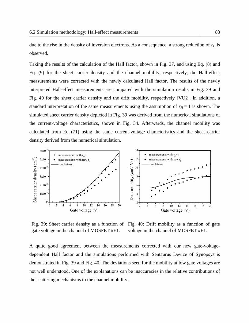
6.2 Simulation methodology: Hall-effect measurements 83
due to the rise in the density of inversion electrons. As a consequence, a strong reduction of rH is
observed.
Taking the results of the calculation of the Hall factor, shown in Fig. 37, and using Eq. (8) and
Eq. (9) for the sheet carrier density and the channel mobility, respectively, the Hall-effect
measurements were corrected with the newly calculated Hall factor. The results of the newly
interpreted Hall-effect measurements are compared with the simulation results in Fig. 39 and
Fig. 40 for the sheet carrier density and the drift mobility, respectively [VU2]. In addition, a
standard interpretation of the same measurements using the assumption of rH = 1 is shown. The
simulated sheet carrier density depicted in Fig. 39 was derived from the numerical simulations of
the current-voltage characteristics, shown in Fig. 34. Afterwards, the channel mobility was
calculated from Eq. (71) using the same current-voltage characteristics and the sheet carrier
density derived from the numerical simulation.
Fig. 39: Sheet carrier density as a function of
gate voltage in the channel of MOSFET #E1.
Fig. 40: Drift mobility as a function of gate
voltage in the channel of MOSFET #E1.
A quite good agreement between the measurements corrected with our new gate-voltage-
dependent Hall factor and the simulations performed with Sentaurus Device of Synopsys is
demonstrated in Fig. 39 and Fig. 40. The deviations seen for the mobility at low gate voltages are
not well understood. One of the explanations can be inaccuracies in the relative contributions of
the scattering mechanisms to the channel mobility.
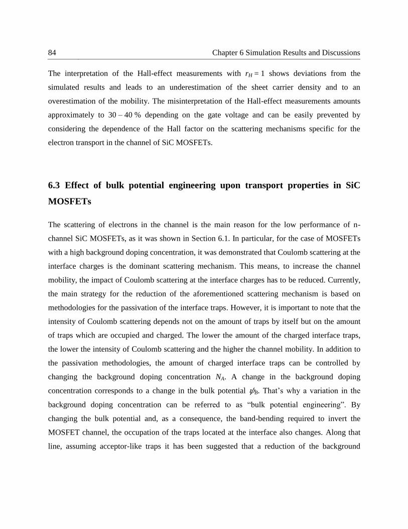
84 Chapter 6 Simulation Results and Discussions
The interpretation of the Hall-effect measurements with rH = 1 shows deviations from the
simulated results and leads to an underestimation of the sheet carrier density and to an
overestimation of the mobility. The misinterpretation of the Hall-effect measurements amounts
approximately to 30 – 40 % depending on the gate voltage and can be easily prevented by
considering the dependence of the Hall factor on the scattering mechanisms specific for the
electron transport in the channel of SiC MOSFETs.
6.3 Effect of bulk potential engineering upon transport properties in SiC
MOSFETs
The scattering of electrons in the channel is the main reason for the low performance of n-
channel SiC MOSFETs, as it was shown in Section 6.1. In particular, for the case of MOSFETs
with a high background doping concentration, it was demonstrated that Coulomb scattering at the
interface charges is the dominant scattering mechanism. This means, to increase the channel
mobility, the impact of Coulomb scattering at the interface charges has to be reduced. Currently,
the main strategy for the reduction of the aforementioned scattering mechanism is based on
methodologies for the passivation of the interface traps. However, it is important to note that the
intensity of Coulomb scattering depends not on the amount of traps by itself but on the amount
of traps which are occupied and charged. The lower the amount of the charged interface traps,
the lower the intensity of Coulomb scattering and the higher the channel mobility. In addition to
the passivation methodologies, the amount of charged interface traps can be controlled by
changing the background doping concentration NA. A change in the background doping
concentration corresponds to a change in the bulk potential 𝜓B. That’s why a variation in the
background doping concentration can be referred to as “bulk potential engineering”. By
changing the bulk potential and, as a consequence, the band-bending required to invert the
MOSFET channel, the occupation of the traps located at the interface also changes. Along that
line, assuming acceptor-like traps it has been suggested that a reduction of the background
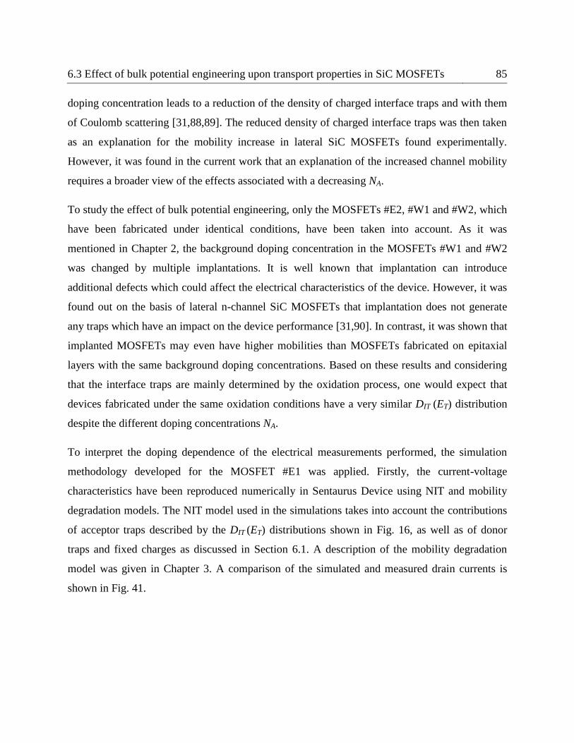
6.3 Effect of bulk potential engineering upon transport properties in SiC MOSFETs 85
doping concentration leads to a reduction of the density of charged interface traps and with them
of Coulomb scattering [31,88,89]. The reduced density of charged interface traps was then taken
as an explanation for the mobility increase in lateral SiC MOSFETs found experimentally.
However, it was found in the current work that an explanation of the increased channel mobility
requires a broader view of the effects associated with a decreasing NA.
To study the effect of bulk potential engineering, only the MOSFETs #E2, #W1 and #W2, which
have been fabricated under identical conditions, have been taken into account. As it was
mentioned in Chapter 2, the background doping concentration in the MOSFETs #W1 and #W2
was changed by multiple implantations. It is well known that implantation can introduce
additional defects which could affect the electrical characteristics of the device. However, it was
found out on the basis of lateral n-channel SiC MOSFETs that implantation does not generate
any traps which have an impact on the device performance [31,90]. In contrast, it was shown that
implanted MOSFETs may even have higher mobilities than MOSFETs fabricated on epitaxial
layers with the same background doping concentrations. Based on these results and considering
that the interface traps are mainly determined by the oxidation process, one would expect that
devices fabricated under the same oxidation conditions have a very similar DIT (ET) distribution
despite the different doping concentrations NA.
To interpret the doping dependence of the electrical measurements performed, the simulation
methodology developed for the MOSFET #E1 was applied. Firstly, the current-voltage
characteristics have been reproduced numerically in Sentaurus Device using NIT and mobility
degradation models. The NIT model used in the simulations takes into account the contributions
of acceptor traps described by the DIT (ET) distributions shown in Fig. 16, as well as of donor
traps and fixed charges as discussed in Section 6.1. A description of the mobility degradation
model was given in Chapter 3. A comparison of the simulated and measured drain currents is
shown in Fig. 41.
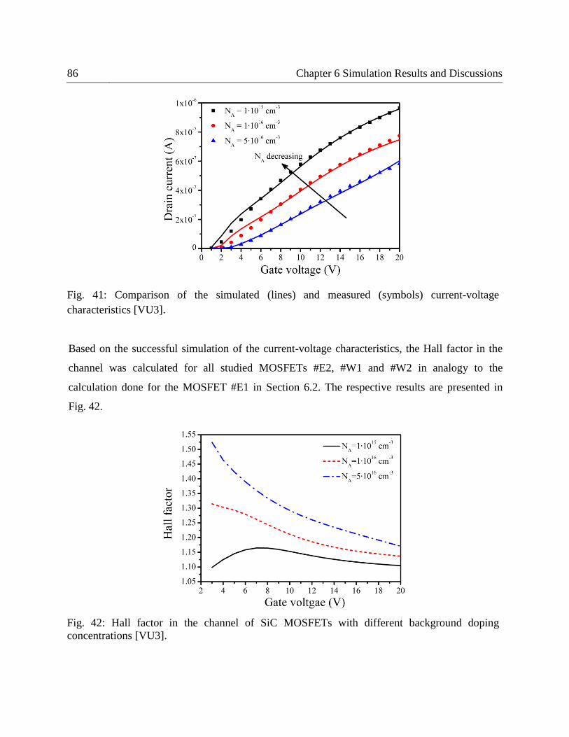
86 Chapter 6 Simulation Results and Discussions
Fig. 41: Comparison of the simulated (lines) and measured (symbols) current-voltage
characteristics [VU3].
Based on the successful simulation of the current-voltage characteristics, the Hall factor in the
channel was calculated for all studied MOSFETs #E2, #W1 and #W2 in analogy to the
calculation done for the MOSFET #E1 in Section 6.2. The respective results are presented in
Fig. 42.
Fig. 42: Hall factor in the channel of SiC MOSFETs with different background doping
concentrations [VU3].
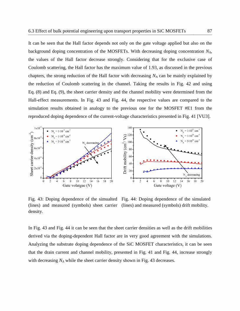
6.3 Effect of bulk potential engineering upon transport properties in SiC MOSFETs 87
It can be seen that the Hall factor depends not only on the gate voltage applied but also on the
background doping concentration of the MOSFETs. With decreasing doping concentration NA,
the values of the Hall factor decrease strongly. Considering that for the exclusive case of
Coulomb scattering, the Hall factor has the maximum value of 1.93, as discussed in the previous
chapters, the strong reduction of the Hall factor with decreasing NA can be mainly explained by
the reduction of Coulomb scattering in the channel. Taking the results in Fig. 42 and using
Eq. (8) and Eq. (9), the sheet carrier density and the channel mobility were determined from the
Hall-effect measurements. In Fig. 43 and Fig. 44, the respective values are compared to the
simulation results obtained in analogy to the previous one for the MOSFET #E1 from the
reproduced doping dependence of the current-voltage characteristics presented in Fig. 41 [VU3].
Fig. 43: Doping dependence of the simualted
(lines) and measured (symbols) sheet carrier
density.
Fig. 44: Doping dependence of the simulated
(lines) and measured (symbols) drift mobility.
In Fig. 43 and Fig. 44 it can be seen that the sheet carrier densities as well as the drift mobilities
derived via the doping-dependent Hall factor are in very good agreement with the simulations.
Analyzing the substrate doping dependence of the SiC MOSFET characteristics, it can be seen
that the drain current and channel mobility, presented in Fig. 41 and Fig. 44, increase strongly
with decreasing NA while the sheet carrier density shown in Fig. 43 decreases.
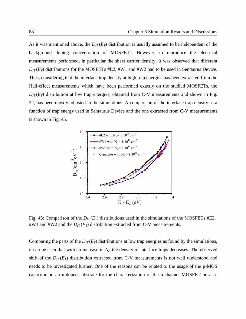
88 Chapter 6 Simulation Results and Discussions
As it was mentioned above, the DIT (ET) distribution is usually assumed to be independent of the
background doping concentration of MOSFETs. However, to reproduce the electrical
measurements performed, in particular the sheet carrier density, it was observed that different
DIT (ET) distributions for the MOSFETs #E2, #W1 and #W2 had to be used in Sentaurus Device.
Thus, considering that the interface trap density at high trap energies has been extracted from the
Hall-effect measurements which have been performed exactly on the studied MOSFETs, the
DIT (ET) distribution at low trap energies, obtained from C-V measurements and shown in Fig.
22, has been mostly adjusted in the simulations. A comparison of the interface trap density as a
function of trap energy used in Sentaurus Device and the one extracted from C-V measurements
is shown in Fig. 45.
Fig. 45: Comparison of the DIT (ET) distributions used in the simulations of the MOSFETs #E2,
#W1 and #W2 and the DIT (ET) distribution extracted from C-V measurements.
Comparing the parts of the DIT (ET) distributions at low trap energies as found by the simulations,
it can be seen that with an increase in NA the density of interface traps decreases. The observed
shift of the DIT (ET) distribution extracted from C-V measurements is not well understood and
needs to be investigated further. One of the reasons can be related to the usage of the p-MOS
capacitor on an n-doped substrate for the characterization of the n-channel MOSFET on a p-
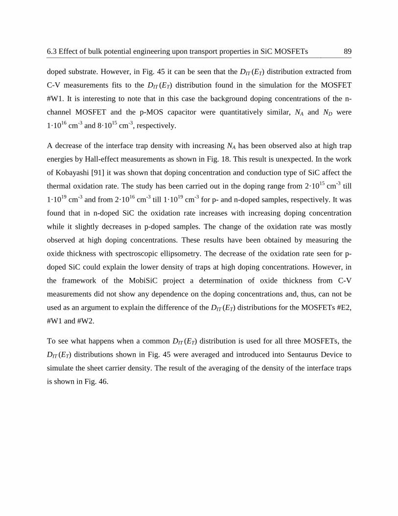
6.3 Effect of bulk potential engineering upon transport properties in SiC MOSFETs 89
doped substrate. However, in Fig. 45 it can be seen that the DIT (ET) distribution extracted from
C-V measurements fits to the DIT (ET) distribution found in the simulation for the MOSFET
#W1. It is interesting to note that in this case the background doping concentrations of the n-
channel MOSFET and the p-MOS capacitor were quantitatively similar, NA and ND were
1·1016
cm-3
and 8·1015
cm-3
, respectively.
A decrease of the interface trap density with increasing NA has been observed also at high trap
energies by Hall-effect measurements as shown in Fig. 18. This result is unexpected. In the work
of Kobayashi [91] it was shown that doping concentration and conduction type of SiC affect the
thermal oxidation rate. The study has been carried out in the doping range from 2·1015
cm-3
till
1·1019
cm-3
and from 2·1016
cm-3
till 1·1019
cm-3
for p- and n-doped samples, respectively. It was
found that in n-doped SiC the oxidation rate increases with increasing doping concentration
while it slightly decreases in p-doped samples. The change of the oxidation rate was mostly
observed at high doping concentrations. These results have been obtained by measuring the
oxide thickness with spectroscopic ellipsometry. The decrease of the oxidation rate seen for p-
doped SiC could explain the lower density of traps at high doping concentrations. However, in
the framework of the MobiSiC project a determination of oxide thickness from C-V
measurements did not show any dependence on the doping concentrations and, thus, can not be
used as an argument to explain the difference of the DIT (ET) distributions for the MOSFETs #E2,
#W1 and #W2.
To see what happens when a common DIT (ET) distribution is used for all three MOSFETs, the
DIT (ET) distributions shown in Fig. 45 were averaged and introduced into Sentaurus Device to
simulate the sheet carrier density. The result of the averaging of the density of the interface traps
is shown in Fig. 46.
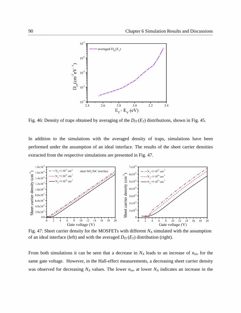
90 Chapter 6 Simulation Results and Discussions
Fig. 46: Density of traps obtained by averaging of the DIT (ET) distributions, shown in Fig. 45.
In addition to the simulations with the averaged density of traps, simulations have been
performed under the assumption of an ideal interface. The results of the sheet carrier densities
extracted from the respective simulations are presented in Fig. 47.
Fig. 47: Sheet carrier density for the MOSFETs with different NA simulated with the assumption
of an ideal interface (left) and with the averaged DIT (ET) distribution (right).
From both simulations it can be seen that a decrease in NA leads to an increase of ninv for the
same gate voltage. However, in the Hall-effect measurements, a decreasing sheet carrier density
was observed for decreasing NA values. The lower ninv at lower NA indicates an increase in the
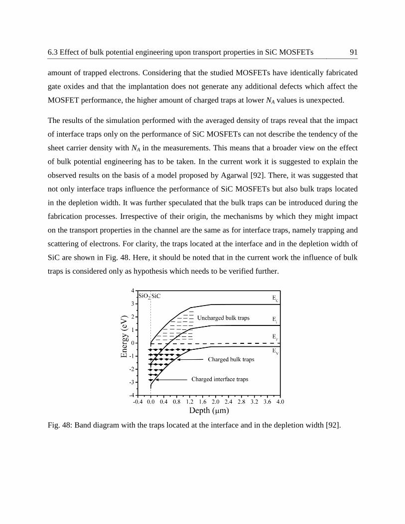
6.3 Effect of bulk potential engineering upon transport properties in SiC MOSFETs 91
amount of trapped electrons. Considering that the studied MOSFETs have identically fabricated
gate oxides and that the implantation does not generate any additional defects which affect the
MOSFET performance, the higher amount of charged traps at lower NA values is unexpected.
The results of the simulation performed with the averaged density of traps reveal that the impact
of interface traps only on the performance of SiC MOSFETs can not describe the tendency of the
sheet carrier density with NA in the measurements. This means that a broader view on the effect
of bulk potential engineering has to be taken. In the current work it is suggested to explain the
observed results on the basis of a model proposed by Agarwal [92]. There, it was suggested that
not only interface traps influence the performance of SiC MOSFETs but also bulk traps located
in the depletion width. It was further speculated that the bulk traps can be introduced during the
fabrication processes. Irrespective of their origin, the mechanisms by which they might impact
on the transport properties in the channel are the same as for interface traps, namely trapping and
scattering of electrons. For clarity, the traps located at the interface and in the depletion width of
SiC are shown in Fig. 48. Here, it should be noted that in the current work the influence of bulk
traps is considered only as hypothesis which needs to be verified further.
Fig. 48: Band diagram with the traps located at the interface and in the depletion width [92].
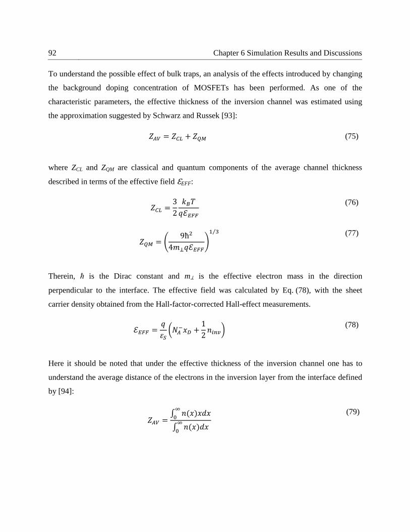
92 Chapter 6 Simulation Results and Discussions
To understand the possible effect of bulk traps, an analysis of the effects introduced by changing
the background doping concentration of MOSFETs has been performed. As one of the
characteristic parameters, the effective thickness of the inversion channel was estimated using
the approximation suggested by Schwarz and Russek [93]:
𝑍𝐴𝑉 = 𝑍𝐶𝐿 + 𝑍𝑄𝑀 (75)
where ZCL and ZQM are classical and quantum components of the average channel thickness
described in terms of the effective field ƐEFF:
𝑍𝐶𝐿 =3
2
𝑘𝐵𝑇
𝑞ℰ𝐸𝐹𝐹
(76)
𝑍𝑄𝑀 = (9ħ2
4𝑚⊥𝑞ℰ𝐸𝐹𝐹)
1 3⁄
(77)
Therein, ħ is the Dirac constant and m⊥ is the effective electron mass in the direction
perpendicular to the interface. The effective field was calculated by Eq. (78), with the sheet
carrier density obtained from the Hall-factor-corrected Hall-effect measurements.
ℰ𝐸𝐹𝐹 =𝑞
휀𝑆(𝑁𝐴
−𝑥𝐷 +1
2𝑛𝑖𝑛𝑣)
(78)
Here it should be noted that under the effective thickness of the inversion channel one has to
understand the average distance of the electrons in the inversion layer from the interface defined
by [94]:
𝑍𝐴𝑉 =∫ 𝑛(𝑥)𝑥𝑑𝑥∞
0
∫ 𝑛(𝑥)𝑑𝑥∞
0
(79)
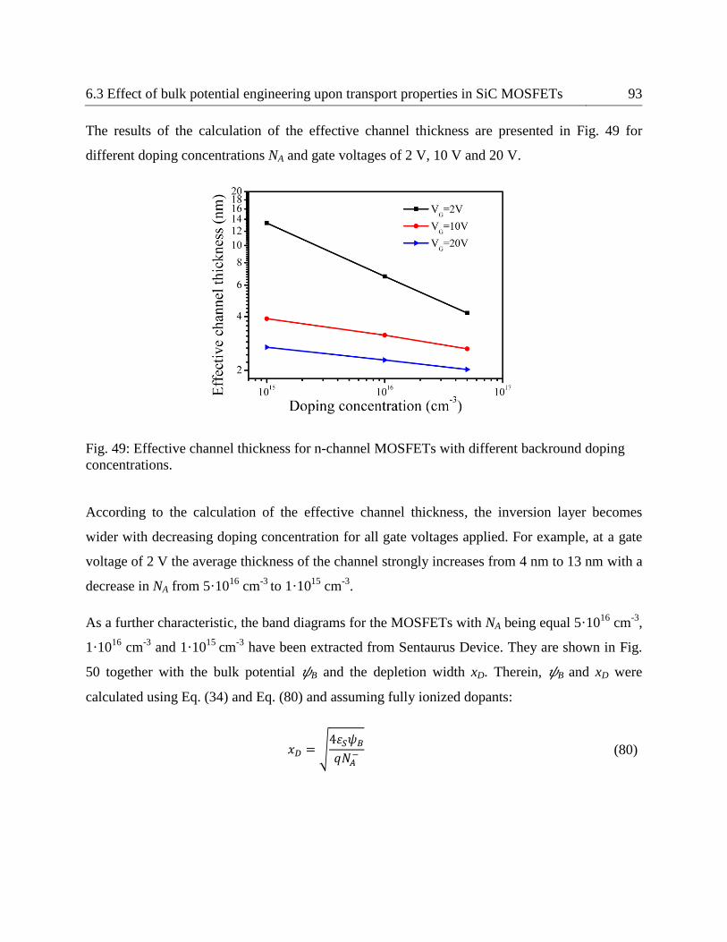
6.3 Effect of bulk potential engineering upon transport properties in SiC MOSFETs 93
The results of the calculation of the effective channel thickness are presented in Fig. 49 for
different doping concentrations NA and gate voltages of 2 V, 10 V and 20 V.
Fig. 49: Effective channel thickness for n-channel MOSFETs with different backround doping
concentrations.
According to the calculation of the effective channel thickness, the inversion layer becomes
wider with decreasing doping concentration for all gate voltages applied. For example, at a gate
voltage of 2 V the average thickness of the channel strongly increases from 4 nm to 13 nm with a
decrease in NA from 5·1016
cm-3
to 1·1015
cm-3
.
As a further characteristic, the band diagrams for the MOSFETs with NA being equal 5·1016
cm-3
,
1·1016
cm-3
and 1·1015
cm-3
have been extracted from Sentaurus Device. They are shown in Fig.
50 together with the bulk potential 𝜓B and the depletion width xD. Therein, 𝜓B and xD were
calculated using Eq. (34) and Eq. (80) and assuming fully ionized dopants:
𝑥𝐷 = √4휀𝑆𝜓𝐵𝑞𝑁𝐴
−
(80)
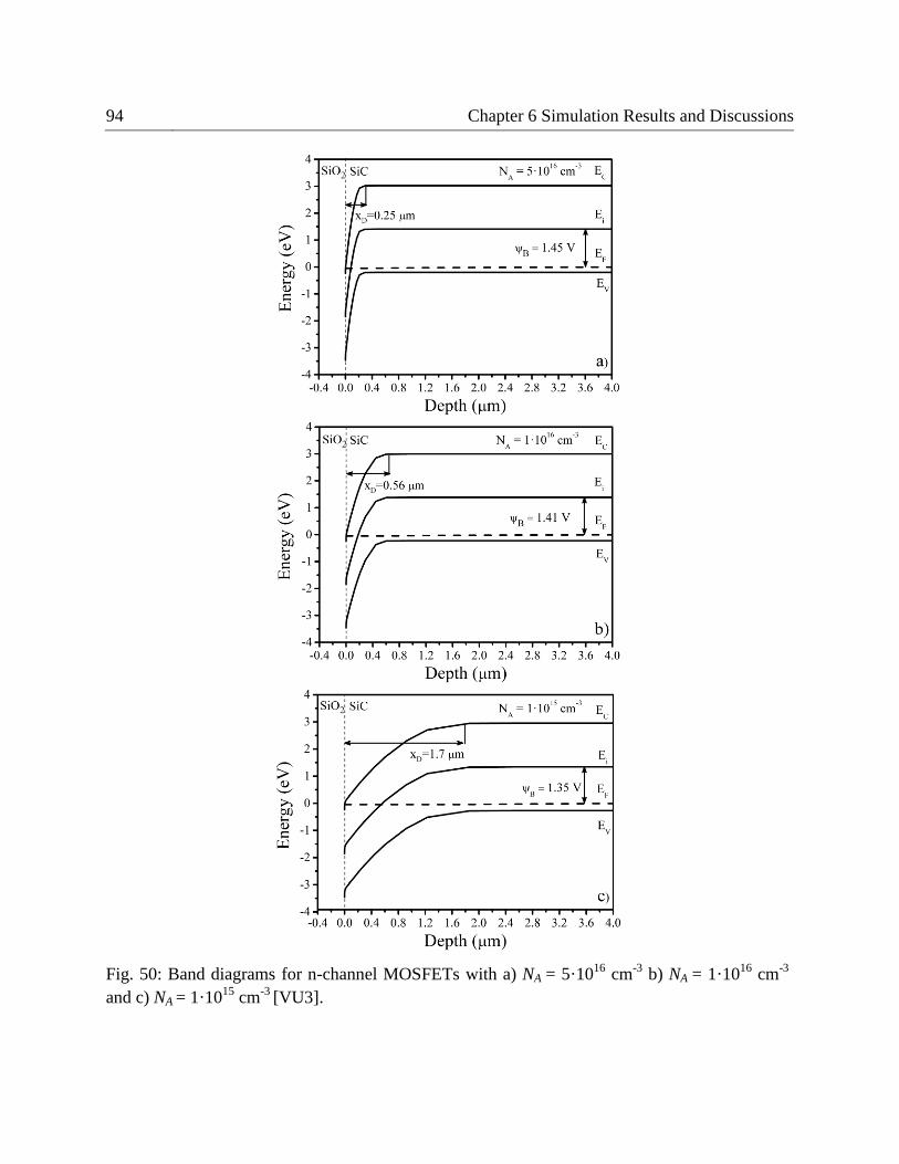
94 Chapter 6 Simulation Results and Discussions
Fig. 50: Band diagrams for n-channel MOSFETs with a) NA = 5·1016
cm-3
b) NA = 1·1016
cm-3
and c) NA = 1·1015
cm-3
[VU3].
6.3 Effect of bulk potential engineering upon transport properties in SiC MOSFETs 95
From the comparison of the band diagrams, shown above, it can be seen that with a decrease in
NA from 5·1016
cm-3
to 1·1015
cm-3
, 𝜓B decreases only from 1.45 V to 1.35 V while xD changes
strongly and shows an increase from 0.25 𝜇m to 1.7 𝜇m.
Summarizing the results obtained, a decrease of the background doping concentration of
MOSFETs leads to:
a decrease of the bulk potential;
an increase of the depletion width;
an increase of the inversion channel thickness;
Thus, the lower sheet carrier density observed in the measurements at lower NA can be explained
by the following hypothesis. Considering that at high doping concentrations the depletion width
is small and that the inversion layer is located close to the interface, the sheet carrier density as
well as the channel mobility is determined mainly by the traps located at the interface. With
decreasing NA the depletion region as well as the inversion layer become wider and more and
more bulk traps will affect the electron transport in the channel of the transistor in addition to the
interface traps, leading to the observed decrease of the sheet carrier density.
Considering that the interface and bulk traps have electrically the same impact on the device
characteristics, i.e. trapping and scattering of electrons from the inversion channel, the two kinds
of traps can not be distinguished from the measurements performed. Thus, the density of traps
extracted from the Hall-effect and C-V measurements is a sum of the densities of the interface
and bulk traps. Taking the different contributions of the bulk traps at different doping
concentrations into account, the difference of the DIT (ET) distributions, observed for the studied
MOSFETs and shown in Fig. 45, can be explained.
Based on the existing models of traps in Sentaurus Device a qualitative analysis of the impact of
bulk traps upon transport properties in the channel of SiC MOSFETs has been performed. For
this purpose, the sheet carrier densities of the MOSFETs with NA of 1·1015
cm-3
, 1·1016
cm-3
,
5·1016
cm-3
have been simulated considering the effect from the bulk traps only. A homogeneous
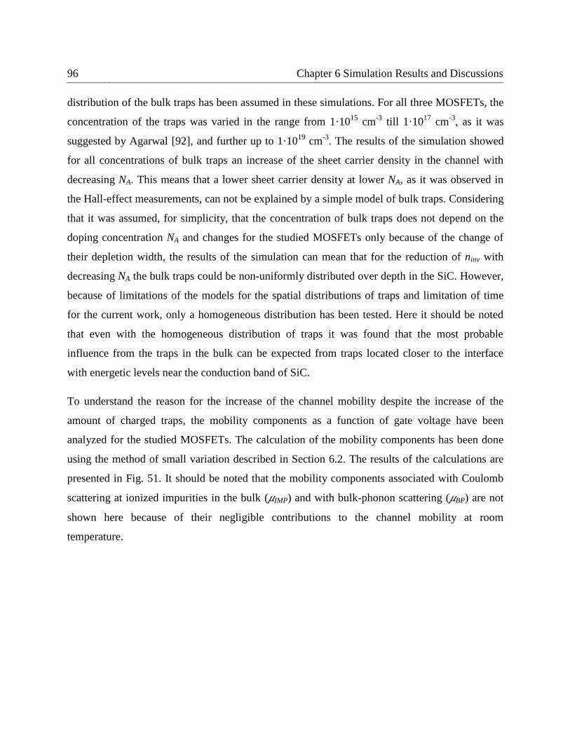
96 Chapter 6 Simulation Results and Discussions
distribution of the bulk traps has been assumed in these simulations. For all three MOSFETs, the
concentration of the traps was varied in the range from 1·1015
cm-3
till 1·1017
cm-3
, as it was
suggested by Agarwal [92], and further up to 1·1019
cm-3
. The results of the simulation showed
for all concentrations of bulk traps an increase of the sheet carrier density in the channel with
decreasing NA. This means that a lower sheet carrier density at lower NA, as it was observed in
the Hall-effect measurements, can not be explained by a simple model of bulk traps. Considering
that it was assumed, for simplicity, that the concentration of bulk traps does not depend on the
doping concentration NA and changes for the studied MOSFETs only because of the change of
their depletion width, the results of the simulation can mean that for the reduction of ninv with
decreasing NA the bulk traps could be non-uniformly distributed over depth in the SiC. However,
because of limitations of the models for the spatial distributions of traps and limitation of time
for the current work, only a homogeneous distribution has been tested. Here it should be noted
that even with the homogeneous distribution of traps it was found that the most probable
influence from the traps in the bulk can be expected from traps located closer to the interface
with energetic levels near the conduction band of SiC.
To understand the reason for the increase of the channel mobility despite the increase of the
amount of charged traps, the mobility components as a function of gate voltage have been
analyzed for the studied MOSFETs. The calculation of the mobility components has been done
using the method of small variation described in Section 6.2. The results of the calculations are
presented in Fig. 51. It should be noted that the mobility components associated with Coulomb
scattering at ionized impurities in the bulk (𝜇IMP) and with bulk-phonon scattering (𝜇BP) are not
shown here because of their negligible contributions to the channel mobility at room
temperature.
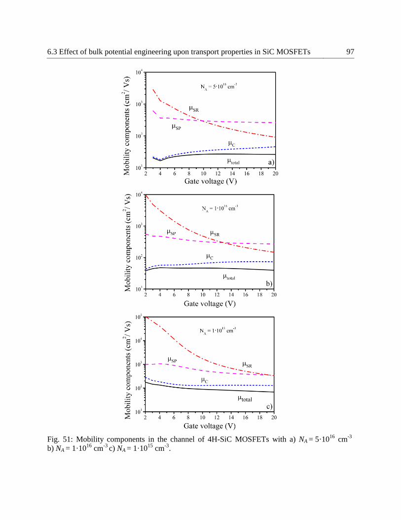
6.3 Effect of bulk potential engineering upon transport properties in SiC MOSFETs 97
Fig. 51: Mobility components in the channel of 4H-SiC MOSFETs with a) NA = 5·1016
cm-3
b) NA = 1·1016
cm-3
c) NA = 1·1015
cm-3
.
98 Chapter 6 Simulation Results and Discussions
From the comparison of the most relevant mobility components in Fig. 51, it can be seen that
Coulomb scattering at the interface charges is the dominant scattering mechanism at room
temperature for all doping concentrations and gate voltages. With decreasing doping
concentration the mobility component associated with Coulomb scattering at the interface
charges increases strongly. As a result, the channel mobility also increases with decreasing
doping concentration. For clarity, the mobility component 𝜇C is shown separately in Fig. 52 for
the studied MOSFETs. The increase of 𝜇C indicates a reduction of Coulomb scattering at the
charged traps despite the higher amount of charged traps at lower NA as discussed above. This
means that the impact of the charged traps upon the channel mobility decreases with decreasing
doping concentration.
Fig. 52: Mobility component associated with Coulomb scattering at the interface (𝜇C) in the
channel of SiC MOSFETs with different background doping concentrations.
Here it should be noted that in the current simulation the effect of the decrease of Coulomb
scattering at the interface charges despite the higher density of interface traps has been achieved
artificially by the calibration of the model for 𝜇C to reproduce the electrical measurements.
However, taking into account the model of Agarwal who suggests the existence of bulk traps, the
increase of the channel mobility with decreasing doping concentration can be explained by the
combination of several mechanisms. Firstly, the additional charged bulk traps at lower values of
6.4 On the temperature dependence of the electrical characteristics of SiC MOSFETs 99
NA contribute additionally to Coulomb scattering of the channel electrons. However, since the
density of the bulk traps is usually much smaller than the local density of the traps at the
interface, Coulomb scattering at the former should be much smaller than at the latter. Secondly,
due to the decrease of the bulk potential with decreasing NA, the amount of the charged interface
traps decreases. Finally, since the thickness of the inversion layer depends on the doping
concentrations, the depth dependence of the mobility in the transistor plays a role. In the work of
Potbhare [44] it was shown that the local mobility of SiC MOSFETs strongly increases when
moving away from the interface into the bulk of the SiC crystal. This was explained by the quick
decrease of the Coulomb potential which leads to a lower impact of the charged interface traps
on mobility. Considering that with decreasing background doping concentration, the thickness of
the channel increases, the channel mobility also increases. Thus, the influence of bulk potential
engineering on the transport properties in the channel of SiC MOSFETs can be explained by the
combination of several effects, discussed above, which result in a lower sheet carrier density but
in a much higher channel mobility and drain current at lower background doping concentrations.
6.4 On the temperature dependence of the electrical characteristics of SiC
MOSFETs
Since SiC MOSFETs are well suited for operation at high temperatures due to the SiC material
properties, the temperature dependence of the electrical characteristics of n-channel 4H-SiC
MOSFETs was studied. For this purpose, in the current work, current-voltage and Hall-effect
measurements have been numerically simulated in the temperature range from 300 K till 400 K
for the MOSFET #E1 and from 300 K till 500 K for the MOSFET #E2. For the other MOSFETs,
no temperature-dependent measurements were available from the MobiSiC project.
It is well known that the temperature variation has two main effects on the transport properties in
the channel of SiC MOSFETs. The first one is a change in the contributions of the scattering
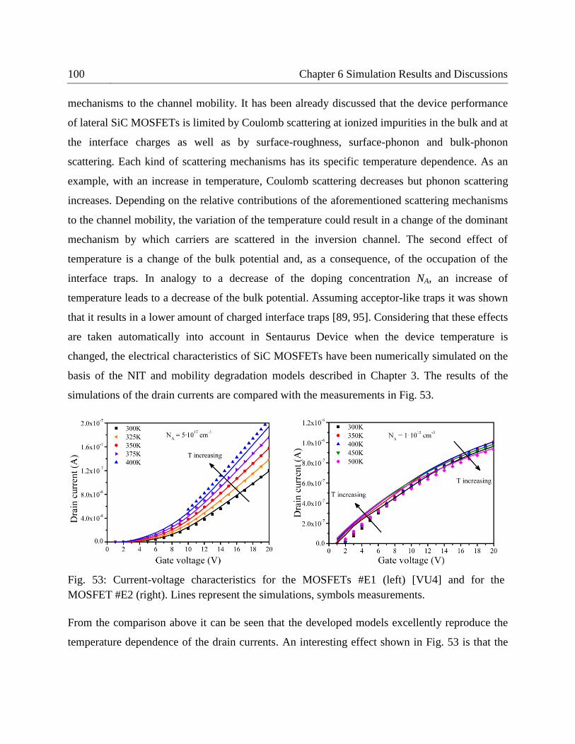
100 Chapter 6 Simulation Results and Discussions
mechanisms to the channel mobility. It has been already discussed that the device performance
of lateral SiC MOSFETs is limited by Coulomb scattering at ionized impurities in the bulk and at
the interface charges as well as by surface-roughness, surface-phonon and bulk-phonon
scattering. Each kind of scattering mechanisms has its specific temperature dependence. As an
example, with an increase in temperature, Coulomb scattering decreases but phonon scattering
increases. Depending on the relative contributions of the aforementioned scattering mechanisms
to the channel mobility, the variation of the temperature could result in a change of the dominant
mechanism by which carriers are scattered in the inversion channel. The second effect of
temperature is a change of the bulk potential and, as a consequence, of the occupation of the
interface traps. In analogy to a decrease of the doping concentration NA, an increase of
temperature leads to a decrease of the bulk potential. Assuming acceptor-like traps it was shown
that it results in a lower amount of charged interface traps [89, 95]. Considering that these effects
are taken automatically into account in Sentaurus Device when the device temperature is
changed, the electrical characteristics of SiC MOSFETs have been numerically simulated on the
basis of the NIT and mobility degradation models described in Chapter 3. The results of the
simulations of the drain currents are compared with the measurements in Fig. 53.
Fig. 53: Current-voltage characteristics for the MOSFETs #E1 (left) [VU4] and for the
MOSFET #E2 (right). Lines represent the simulations, symbols measurements.
From the comparison above it can be seen that the developed models excellently reproduce the
temperature dependence of the drain currents. An interesting effect shown in Fig. 53 is that the
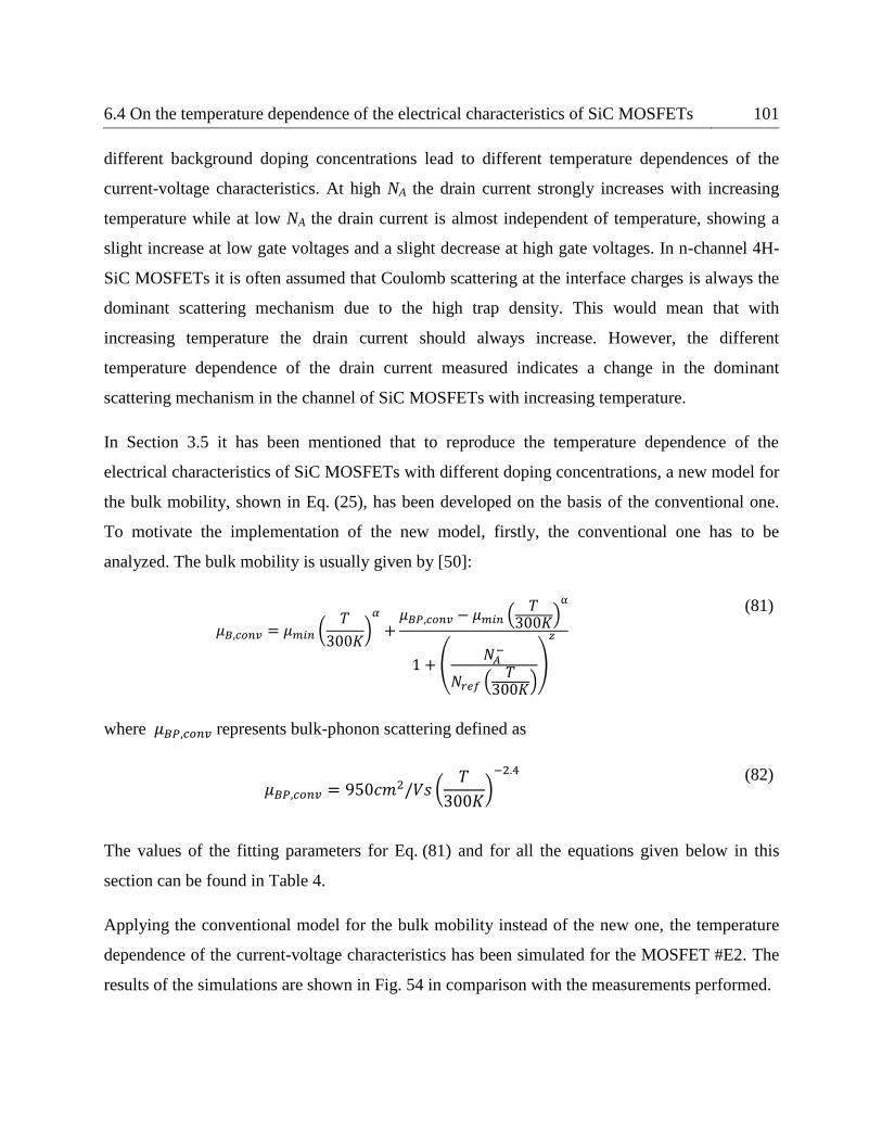
6.4 On the temperature dependence of the electrical characteristics of SiC MOSFETs 101
different background doping concentrations lead to different temperature dependences of the
current-voltage characteristics. At high NA the drain current strongly increases with increasing
temperature while at low NA the drain current is almost independent of temperature, showing a
slight increase at low gate voltages and a slight decrease at high gate voltages. In n-channel 4H-
SiC MOSFETs it is often assumed that Coulomb scattering at the interface charges is always the
dominant scattering mechanism due to the high trap density. This would mean that with
increasing temperature the drain current should always increase. However, the different
temperature dependence of the drain current measured indicates a change in the dominant
scattering mechanism in the channel of SiC MOSFETs with increasing temperature.
In Section 3.5 it has been mentioned that to reproduce the temperature dependence of the
electrical characteristics of SiC MOSFETs with different doping concentrations, a new model for
the bulk mobility, shown in Eq. (25), has been developed on the basis of the conventional one.
To motivate the implementation of the new model, firstly, the conventional one has to be
analyzed. The bulk mobility is usually given by [50]:
𝜇𝐵,𝑐𝑜𝑛𝑣 = 𝜇𝑚𝑖𝑛 (𝑇
300𝐾)𝛼
+𝜇𝐵𝑃,𝑐𝑜𝑛𝑣 − 𝜇𝑚𝑖𝑛 (
𝑇300𝐾)
α
1 + (𝑁𝐴−
𝑁𝑟𝑒𝑓 (𝑇
300𝐾))
𝑧
(81)
where 𝜇𝐵𝑃,𝑐𝑜𝑛𝑣 represents bulk-phonon scattering defined as
𝜇𝐵𝑃,𝑐𝑜𝑛𝑣 = 950𝑐𝑚2/𝑉𝑠 (
𝑇
300𝐾)−2.4
(82)
The values of the fitting parameters for Eq. (81) and for all the equations given below in this
section can be found in Table 4.
Applying the conventional model for the bulk mobility instead of the new one, the temperature
dependence of the current-voltage characteristics has been simulated for the MOSFET #E2. The
results of the simulations are shown in Fig. 54 in comparison with the measurements performed.
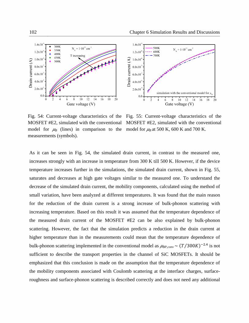
102 Chapter 6 Simulation Results and Discussions
Fig. 54: Current-voltage characteristics of the
MOSFET #E2, simulated with the conventional
model for 𝜇B (lines) in comparison to the
measurements (symbols).
Fig. 55: Current-voltage characteristics of the
MOSFET #E2, simulated with the conventional
model for 𝜇B at 500 K, 600 K and 700 K.
As it can be seen in Fig. 54, the simulated drain current, in contrast to the measured one,
increases strongly with an increase in temperature from 300 K till 500 K. However, if the device
temperature increases further in the simulations, the simulated drain current, shown in Fig. 55,
saturates and decreases at high gate voltages similar to the measured one. To understand the
decrease of the simulated drain current, the mobility components, calculated using the method of
small variation, have been analyzed at different temperatures. It was found that the main reason
for the reduction of the drain current is a strong increase of bulk-phonon scattering with
increasing temperature. Based on this result it was assumed that the temperature dependence of
the measured drain current of the MOSFET #E2 can be also explained by bulk-phonon
scattering. However, the fact that the simulation predicts a reduction in the drain current at
higher temperature than in the measurements could mean that the temperature dependence of
bulk-phonon scattering implemented in the conventional model as 𝜇BP,conv ~ (𝑇 300𝐾⁄ )−2.4 is not
sufficient to describe the transport properties in the channel of SiC MOSFETs. It should be
emphasized that this conclusion is made on the assumption that the temperature dependence of
the mobility components associated with Coulomb scattering at the interface charges, surface-
roughness and surface-phonon scattering is described correctly and does not need any additional
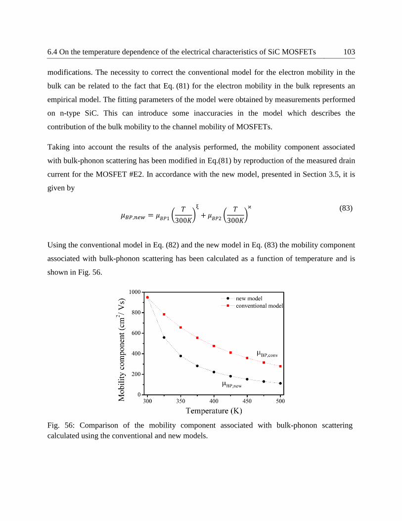
6.4 On the temperature dependence of the electrical characteristics of SiC MOSFETs 103
modifications. The necessity to correct the conventional model for the electron mobility in the
bulk can be related to the fact that Eq. (81) for the electron mobility in the bulk represents an
empirical model. The fitting parameters of the model were obtained by measurements performed
on n-type SiC. This can introduce some inaccuracies in the model which describes the
contribution of the bulk mobility to the channel mobility of MOSFETs.
Taking into account the results of the analysis performed, the mobility component associated
with bulk-phonon scattering has been modified in Eq.(81) by reproduction of the measured drain
current for the MOSFET #E2. In accordance with the new model, presented in Section 3.5, it is
given by
𝜇𝐵𝑃,𝑛𝑒𝑤 = 𝜇𝐵𝑃1 (𝑇
300𝐾)ξ
+ 𝜇𝐵𝑃2(𝑇
300𝐾)ϰ
(83)
Using the conventional model in Eq. (82) and the new model in Eq. (83) the mobility component
associated with bulk-phonon scattering has been calculated as a function of temperature and is
shown in Fig. 56.
Fig. 56: Comparison of the mobility component associated with bulk-phonon scattering
calculated using the conventional and new models.
104 Chapter 6 Simulation Results and Discussions
As it can be seen, to simulate the measured current-voltage characteristics of the MOSFET with
NA = 1·1015
cm-3
, the contribution of bulk-phonon scattering at elevated temperatures has to be
on the average by a factor of two higher than it is predicted by the conventional model. To check
the applicability of the suggested model for higher doping concentrations, this model was applied
in the simulations of the temperature dependence of the electrical characteristics for the
MOSFET #E1 with NA = 5·1017
cm-3
. The simulations of the MOSFET #E1 revealed that the
suggested model leads to some deviations between simulations and measurements because of the
strong reduction of the bulk mobility with increasing temperature. From this result one of the
conclusions could be that bulk-phonon scattering which represents the vibration of the lattice
might depend on the background doping concentration. In the case of high doping
concentrations, the lattice could vibrate less intensively than at low concentrations. At the same
time in Section 3.5 it was mentioned that the mobility in the bulk is determined by two scattering
mechanisms, bulk-phonon scattering and Coulomb scattering at ionized impurities. This means
that another reason for the deviations between simulated and measured electrical properties at
high NA could be an inaccurate description of the impact of Coulomb scattering at ionized
impurities at elevated temperatures. Thus, assuming that bulk-phonon scattering is independent
of doping concentration, Coulomb scattering at ionized impurities was analyzed using the
conventional model presented in Eq. (81). Taking into account that bulk-phonon scattering and
Coulomb scattering at ionized impurities are combined by Matthiessen’s rule as it was shown in
Eq. (24), the mobility component associated with Coulomb scattering at the ionized impurities
𝜇IMP has been calculated by
𝜇𝐼𝑀𝑃 = (1
𝜇𝐵−1
𝜇𝐵𝑃)−1
(84)
where 𝜇B was calculated using the conventional model in Eq. (81). For the bulk-phonon mobility
𝜇BP in Eq. (81) and Eq. (84), the new model in Eq. (83) was used. The result of the calculation is
presented in Fig. 57 for the doping concentrations of 1·1015
cm-3
and 5·1017
cm-3
.
6.4 On the temperature dependence of the electrical characteristics of SiC MOSFETs 105
Fig. 57: Mobility component associated with Coulomb scattering at the ionized impurities,
calculated from the conventional model.
In Fig. 57 it can be seen that the mobility component 𝜇IMP decreases with increasing temperature
from 300 K till 500 K which indicates an increase of Coulomb scattering. However, it is known
that in this temperature range Coulomb scattering at ionized impurities decreases with increasing
temperature which leads to an increase of the mobility limited by ionized impurity scattering
𝜇IMP [96,97]. To avoid the contradiction in the temperature dependence of Coulomb scattering at
ionized impurities, the conventional model was corrected by introducing a term (𝑇 300𝐾⁄ )𝜗 with
𝜗 = -12.5 in the denominator as shown below:
𝜇𝐵 = 𝜇𝑚𝑖𝑛 (𝑇
300𝐾)𝛼
+𝜇𝐵𝑃,𝑛𝑒𝑤 − 𝜇𝑚𝑖𝑛 (
𝑇300𝐾)
α
1 + (𝑇
300𝐾)ϑ
(𝑁𝐴−
𝑁𝑟𝑒𝑓)
𝑧
(85)
It should be noted that in some works [51] the term (𝑇 300𝐾)⁄ 𝜗has been already used but with
much lower absolute value of power coefficient, i.e. 𝜗 was taken -0.76 and 0.73. However, such
powers do not change downward tendency of the temperature dependence of 𝜇IMP. The
106 Chapter 6 Simulation Results and Discussions
correction of Coulomb scattering at the ionized impurities, presented in Eq. (85), has been
obtained from the reproduction of the temperature dependence of the current-voltage
characteristics for both MOSFETs #E1 and #E2, shown in Fig. 53. Using now the new model for
the bulk mobility, the mobility component 𝜇IMP was calculated for 1·1015
cm-3
and 5·1017
cm-3
using Eq. (84). The result of the calculation of 𝜇IMP in comparison to 𝜇BP is shown in Fig. 58.
Therein, it can be seen that the mobility component associated with Coulomb scattering at the
ionized impurities increases now with increasing temperature.
Fig. 58: Mobility components associated with Coulomb scattering at the ionized impurities
(𝜇IMP) and bulk-phonon scattering (𝜇BP), calculated using the new model.
Summarizing the results from the analysis performed, the new model for the electron mobility in
the bulk has been developed assuming:
stronger increase of bulk-phonon scattering with temperature than it is predicted by the
conventional model;
decrease of Coulomb scattering at ionized impurities in the bulk with increasing
temperature;
6.4 On the temperature dependence of the electrical characteristics of SiC MOSFETs 107
Here it should be noted that in the new model at 300 K the ratio of the contributions of 𝜇IMP and
𝜇BP has been taken from the conventional model and unchanged. Although the new model can
well reproduce the characteristics of the studied MOSFETs with two doping concentrations,
1·1015
cm-3
and 5·1017
cm-3
, in the temperature range from 300 K till 500 K, further validation of
the developed model is required for a broader range of doping concentrations and temperatures.
To understand the different dominant scattering mechanisms in the channel of SiC MOSFETs
with high and low NA, the Hall-effect measurements have been analyzed. To interpret the Hall-
effect measurements in a range of temperatures, the Hall factor for the electron transport in the
channel of SiC MOSFETs was calculated as a function of temperature. The results of the
calculation are presented in Fig. 59 for the MOSFETs #E1 and #E2, respectively. Therein, it can
be seen that the values of the Hall factor depend not only on gate voltage and background doping
concentration but also on temperature. The behavior of the Hall factor with temperature reflects
the changes of the relative contributions of the scattering mechanisms. As it is shown in Fig. 59,
with an increase in temperature, the Hall factor in the channel of SiC MOSFETs strongly
decreases for both background doping concentrations.
Fig. 59: Temperature dependence of the Hall factor in the channel of SiC MOSFET #E1 with
NA = 5·1017
cm-3
(left) [VU4] and of the MOSFET #E2 with NA = 1·1015
cm-3
(right).
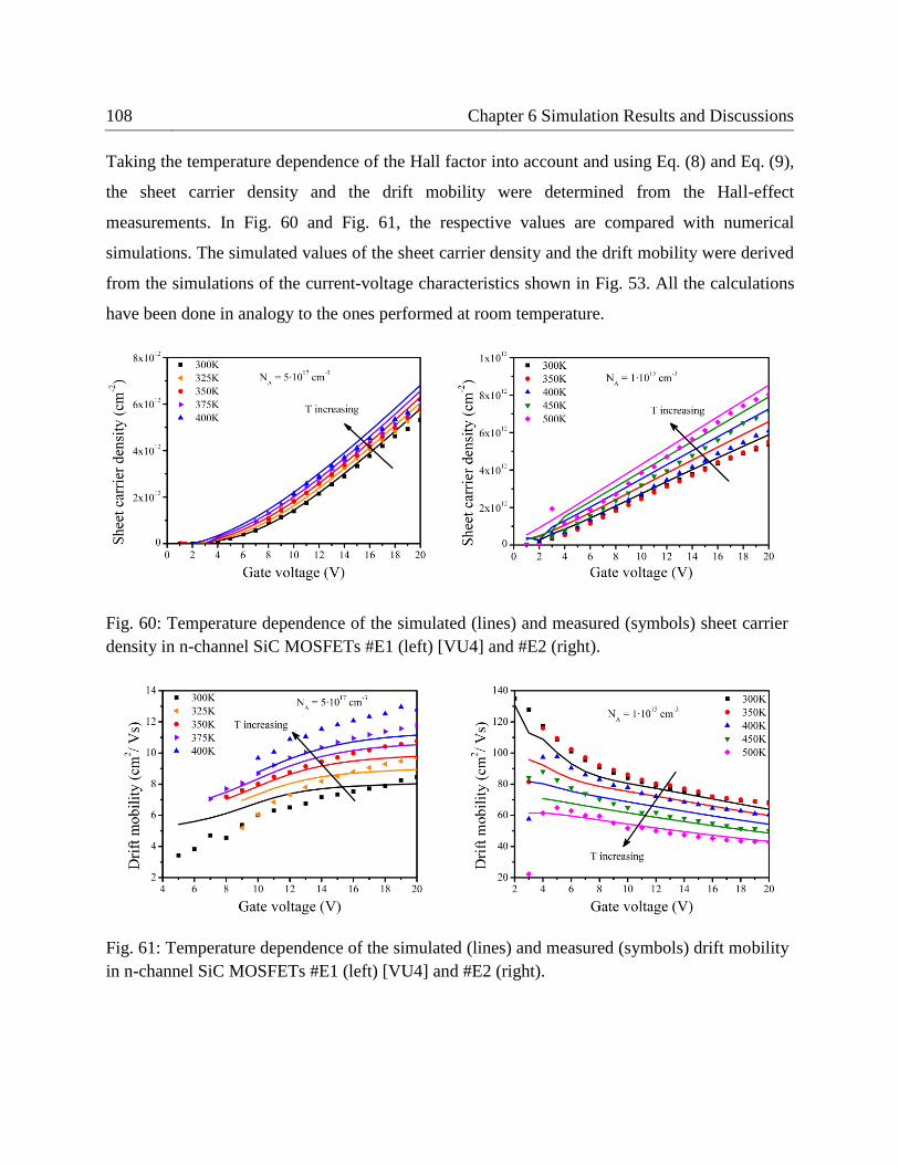
108 Chapter 6 Simulation Results and Discussions
Taking the temperature dependence of the Hall factor into account and using Eq. (8) and Eq. (9),
the sheet carrier density and the drift mobility were determined from the Hall-effect
measurements. In Fig. 60 and Fig. 61, the respective values are compared with numerical
simulations. The simulated values of the sheet carrier density and the drift mobility were derived
from the simulations of the current-voltage characteristics shown in Fig. 53. All the calculations
have been done in analogy to the ones performed at room temperature.
Fig. 60: Temperature dependence of the simulated (lines) and measured (symbols) sheet carrier
density in n-channel SiC MOSFETs #E1 (left) [VU4] and #E2 (right).
Fig. 61: Temperature dependence of the simulated (lines) and measured (symbols) drift mobility
in n-channel SiC MOSFETs #E1 (left) [VU4] and #E2 (right).
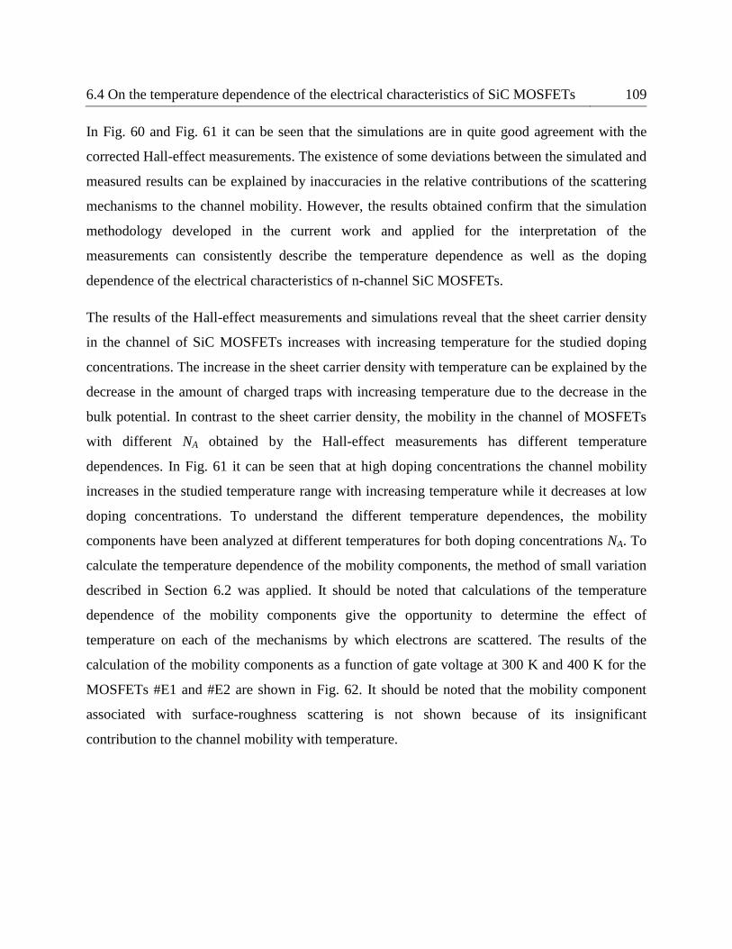
6.4 On the temperature dependence of the electrical characteristics of SiC MOSFETs 109
In Fig. 60 and Fig. 61 it can be seen that the simulations are in quite good agreement with the
corrected Hall-effect measurements. The existence of some deviations between the simulated and
measured results can be explained by inaccuracies in the relative contributions of the scattering
mechanisms to the channel mobility. However, the results obtained confirm that the simulation
methodology developed in the current work and applied for the interpretation of the
measurements can consistently describe the temperature dependence as well as the doping
dependence of the electrical characteristics of n-channel SiC MOSFETs.
The results of the Hall-effect measurements and simulations reveal that the sheet carrier density
in the channel of SiC MOSFETs increases with increasing temperature for the studied doping
concentrations. The increase in the sheet carrier density with temperature can be explained by the
decrease in the amount of charged traps with increasing temperature due to the decrease in the
bulk potential. In contrast to the sheet carrier density, the mobility in the channel of MOSFETs
with different NA obtained by the Hall-effect measurements has different temperature
dependences. In Fig. 61 it can be seen that at high doping concentrations the channel mobility
increases in the studied temperature range with increasing temperature while it decreases at low
doping concentrations. To understand the different temperature dependences, the mobility
components have been analyzed at different temperatures for both doping concentrations NA. To
calculate the temperature dependence of the mobility components, the method of small variation
described in Section 6.2 was applied. It should be noted that calculations of the temperature
dependence of the mobility components give the opportunity to determine the effect of
temperature on each of the mechanisms by which electrons are scattered. The results of the
calculation of the mobility components as a function of gate voltage at 300 K and 400 K for the
MOSFETs #E1 and #E2 are shown in Fig. 62. It should be noted that the mobility component
associated with surface-roughness scattering is not shown because of its insignificant
contribution to the channel mobility with temperature.
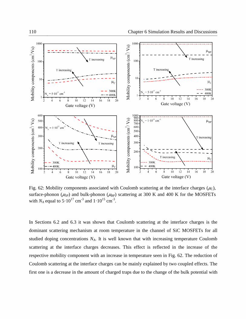
110 Chapter 6 Simulation Results and Discussions
Fig. 62: Mobility components associated with Coulomb scattering at the interface charges (𝜇C),
surface-phonon (𝜇SP) and bulk-phonon (𝜇BP) scattering at 300 K and 400 K for the MOSFETs
with NA equal to 5·1017
cm-3
and 1·1015
cm-3
.
In Sections 6.2 and 6.3 it was shown that Coulomb scattering at the interface charges is the
dominant scattering mechanism at room temperature in the channel of SiC MOSFETs for all
studied doping concentrations NA. It is well known that with increasing temperature Coulomb
scattering at the interface charges decreases. This effect is reflected in the increase of the
respective mobility component with an increase in temperature seen in Fig. 62. The reduction of
Coulomb scattering at the interface charges can be mainly explained by two coupled effects. The
first one is a decrease in the amount of charged traps due to the change of the bulk potential with
6.4 On the temperature dependence of the electrical characteristics of SiC MOSFETs 111
temperature. The second one is an increase in screening of scattering centers due to the increase
of the number of free electrons in the inversion channel. In contrast to Coulomb scattering,
surface-phonon and bulk-phonon scattering increase with an increase in temperature. As a
consequence, the mobility components associated with the aforementioned scattering
mechanisms decrease, as it is shown in Fig. 62. Comparing the total mobilities for the MOSFETs
#E1 and #E2, presented in Fig. 61, with the respective mobility components, the different
temperature dependence of the drain currents and channel mobilities can be explained as
following. The mobility component associated with surface-phonon scattering at high gate
voltages has the same order of magnitude in the MOSFETs #E1 and #E2. Bulk-phonon
scattering, as it was mentioned above, is assumed to be independent of NA and increases equally
with increasing temperature in both MOSFETs. However, the mobility component associated
with Coulomb scattering at the interface charges is on average by a factor of 10 higher in the
MOSFET #E2 than in the MOSFET #E1. This means that in the MOSFET #E1 Coulomb
scattering at the interface charges is much stronger than in the MOSFET #E2, which is reflected
in the lower channel mobility, seen in Fig. 61. Moreover, Coulomb scattering at the interface
charges is so strong in the MOSFET #E1 that the contributions of surface-phonon scattering as
well as bulk-phonon scattering to the channel mobility are negligible even at 400 K. This means
that for the temperature dependence of the SiC MOSFET characteristics with high NA, at least in
the temperature range from 300 K till 400 K, only Coulomb scattering at the interface charges
plays a fundamental role. Considering that Coulomb scattering decreases with an increase in
temperature, the channel mobility increases and, as a consequence, the drain current also
increases. In case of the MOSFET #E2, where Coulomb scattering at the interface charges is
relatively low even at 300 K, an increase of temperature leads to the effect that the contributions
of surface-phonon as well as bulk-phonon scattering become significant. Considering that the
temperature dependence of bulk-phonon scattering is stronger than the temperature dependence
of surface-phonon scattering, 𝜇BP decreases with increasing temperature faster and starts to
dominate at high temperature. This results in the reduction of the channel mobility as well as the
drain current.

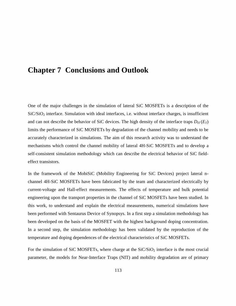
113
Chapter 7 Conclusions and Outlook
One of the major challenges in the simulation of lateral SiC MOSFETs is a description of the
SiC/SiO2 interface. Simulation with ideal interfaces, i.e. without interface charges, is insufficient
and can not describe the behavior of SiC devices. The high density of the interface traps DIT (ET)
limits the performance of SiC MOSFETs by degradation of the channel mobility and needs to be
accurately characterized in simulations. The aim of this research activity was to understand the
mechanisms which control the channel mobility of lateral 4H-SiC MOSFETs and to develop a
self-consistent simulation methodology which can describe the electrical behavior of SiC field-
effect transistors.
In the framework of the MobiSiC (Mobility Engineering for SiC Devices) project lateral n-
channel 4H-SiC MOSFETs have been fabricated by the team and characterized electrically by
current-voltage and Hall-effect measurements. The effects of temperature and bulk potential
engineering upon the transport properties in the channel of SiC MOSFETs have been studied. In
this work, to understand and explain the electrical measurements, numerical simulations have
been performed with Sentaurus Device of Synopsys. In a first step a simulation methodology has
been developed on the basis of the MOSFET with the highest background doping concentration.
In a second step, the simulation methodology has been validated by the reproduction of the
temperature and doping dependences of the electrical characteristics of SiC MOSFETs.
For the simulation of SiC MOSFETs, where charge at the SiC/SiO2 interface is the most crucial
parameter, the models for Near-Interface Traps (NIT) and mobility degradation are of primary
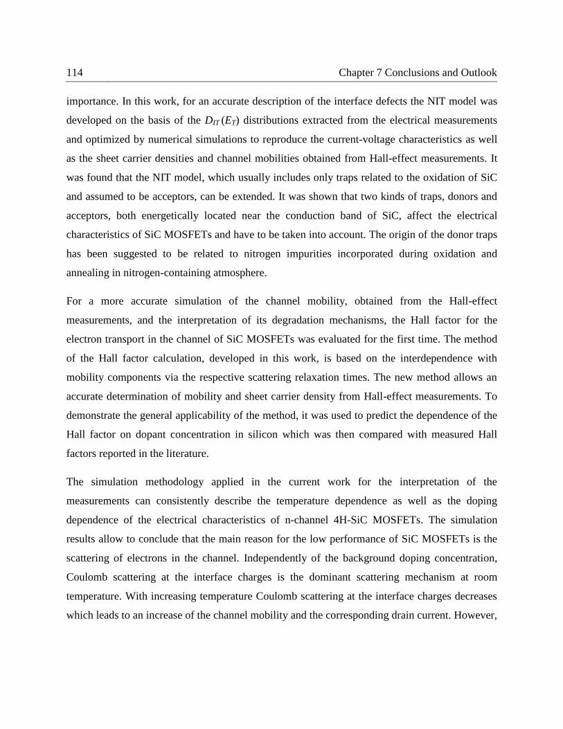
114 Chapter 7 Conclusions and Outlook
importance. In this work, for an accurate description of the interface defects the NIT model was
developed on the basis of the DIT (ET) distributions extracted from the electrical measurements
and optimized by numerical simulations to reproduce the current-voltage characteristics as well
as the sheet carrier densities and channel mobilities obtained from Hall-effect measurements. It
was found that the NIT model, which usually includes only traps related to the oxidation of SiC
and assumed to be acceptors, can be extended. It was shown that two kinds of traps, donors and
acceptors, both energetically located near the conduction band of SiC, affect the electrical
characteristics of SiC MOSFETs and have to be taken into account. The origin of the donor traps
has been suggested to be related to nitrogen impurities incorporated during oxidation and
annealing in nitrogen-containing atmosphere.
For a more accurate simulation of the channel mobility, obtained from the Hall-effect
measurements, and the interpretation of its degradation mechanisms, the Hall factor for the
electron transport in the channel of SiC MOSFETs was evaluated for the first time. The method
of the Hall factor calculation, developed in this work, is based on the interdependence with
mobility components via the respective scattering relaxation times. The new method allows an
accurate determination of mobility and sheet carrier density from Hall-effect measurements. To
demonstrate the general applicability of the method, it was used to predict the dependence of the
Hall factor on dopant concentration in silicon which was then compared with measured Hall
factors reported in the literature.
The simulation methodology applied in the current work for the interpretation of the
measurements can consistently describe the temperature dependence as well as the doping
dependence of the electrical characteristics of n-channel 4H-SiC MOSFETs. The simulation
results allow to conclude that the main reason for the low performance of SiC MOSFETs is the
scattering of electrons in the channel. Independently of the background doping concentration,
Coulomb scattering at the interface charges is the dominant scattering mechanism at room
temperature. With increasing temperature Coulomb scattering at the interface charges decreases
which leads to an increase of the channel mobility and the corresponding drain current. However,
Chapter 7 Conclusions and Outlook 115
phonon scattering increases with increasing temperature. When the contributions from Coulomb
and phonon scattering mechanisms become comparable at high temperatures, the channel
mobility decreases with increasing temperature. In this work, it was found that the temperature
dependence of the electrical characteristics of 4H-SiC MOSFETs depends on the doping
concentration: For highly doped MOSFETs, the channel mobility increases with increasing
temperature while it decreases for lowly doped ones. To reproduce the electrical measurements
for the MOSFETs with low and high background doping concentrations at elevated
temperatures, a new model for the mobility in the bulk has been developed and implemented via
the “Physical Model Interface” of Sentaurus Device. It was found that the conventional model of
bulk-phonon scattering can not reproduce the temperature dependence of the MOSFETs with
low background doping concentration. Based on the simulation analysis performed, the
contribution from bulk-phonon scattering has to be on the average by a factor of two higher than
it is predicted by the conventional model. However, further experimental work, i.e. broader
ranges of temperatures and doping concentrations, is required to confirm the validity of the
newly proposed model.
Considering that at room temperature Coulomb scattering at the interface charges is the
dominant scattering mechanism, its impact has to be reduced to improve the channel mobility.
The intensity of Coulomb scattering at the interface charges depends on the amount of traps
which are occupied and charged. Assuming the presence of acceptor-like traps, one of the
strategies to decrease Coulomb scattering at the interface charges is to decrease the amount of
charged interface traps by decreasing the background doping concentration. The study of this
effect in the current work showed that the explanation of the improvement of the channel
mobility with decreasing background doping concentration needs a broader view than it is
usually presented in literature. One of the effects which have to be taken into account is a
widening of the inversion channel with a decrease of the doping concentration. Considering that
the impact of the interface traps decreases when moving from the interface to the bulk of SiC, the
widening of the inversion layer results in an increase of the channel mobility. This means that a
change of the thickness of the inversion layer affects the channel mobility.
116 Chapter 7 Conclusions and Outlook
Based on the simulations performed it was found that the model currently implemented in
Sentaurus Device for the mobility component associated with Coulomb scattering at the interface
charges can not adequately describe the depth dependence of the mobility. Thus, simulating the
doping dependence of the electrical measurements for SiC MOSFETs, the model has been
artificially calibrated for each studied doping concentration. However, the effect that the mobility
depends on the distance from the interface, and that it changes with doping concentration is very
important. Thus, new models for mobility, which can accurately describe the aforementioned
effect, have to be developed and implemented in simulation software.
Summing up, using Sentaurus Device of Synopsys the electrical measurements performed for
lateral n-channel 4H-SiC MOSFETs at different temperatures and background doping
concentrations have been analyzed and well described using the developed simulation
methodology. The numerical simulations performed are based on silicon models for which the
parameter set has been calibrated. However, to use simulation software as a tool which can
predict the behavior of SiC devices, in particular SiC MOSFETs, simulation models have to be
improved.

117
Acknowledgement
I would like to express my deep gratitude to all those who gave me the possibility to perform this
work and helped me during this time. First of all, I would like to thank my supervisor PD Dr.
Peter Pichler for the patient guidance of my thesis and his support.
Special thanks go to Dr. Alex Burenkov for his supervising, support and advices during this time.
Without his help it would have been difficult for me successfully to complete this work.
I would like also to thank all colleagues with whom I have been working on the MobiSiC
project: Dr. Christian Strenger, Dr. Anton Bauer, Dr. Vincent Mortet, Dr. Elena Bedel-Pereira,
Dr. Guillermo Ortiz and Dr. Cristiano Fuccio.
Big thanks go to Dr. Jürgen Lorenz for giving me the chance to work in the department
Simulation at Fraunhofer IISB and his support.
I would like also to thank all colleagues at Fraunhofer IISB for the warm and friendly
atmosphere during this time.
Last but not least, many thanks go to my family and my friends for their love, support and
consideration.

119
References
[1] B. Ozpineci and L. M. Tolbert, "Comparison of wide-bandgap semiconductors for power
electronics applications", U.S. Dept. of energy report, no. ORNL/TM-2003/257, 2003.
[2] V. V. Afanas’ev, F. Ciobanu, G. Pensl, and A. Stesmans, "Contributions to the density of
interface states in SiC MOS structures," in Silicon carbide: Recent major advances,
Springer, New York, 2004.
[3] S.Dimitrijev and P.Jamet, "Advances in SiC power MOSFET technology," Microelectronics
Reliability, vol. 43, no. 2, pp. 225-233, 2003.
[4] P. Deák, J. M. Knaup, T. Hornos, C. Thill, A. Gali, and T. Frauenheim, "The mechanism of
defect creation and passivation at the SiC/SiO2 interface," Journal of Physics D: Applied
Physics, vol. 40, pp. 6242-6253, 2007.
[5] P. Jamet, S. Dimitrijev, and P. Tanner, "Effects of nitridation in gate oxides grown on 4H-
SiC," Journal of Applied Physics, vol. 90, no. 10, pp. 5058-5063, 2001.
[6] M. K. Das, G. Chung, J. R. Williams, N. Saks, L. A. Lipkin, and J. W. Palmour, "High-
current, NO-annealed lateral 4H-SiC MOSFETs," Materials Science Forum, vol. 389-393,
pp. 981-984, 2002.
[7] L. A. Lipkin, M. K. Das, and J. W. Palmour, "N2O processing improves the 4H-SiC:SiO2
interface," Materials Science Forum, vol. 389-393, pp. 985-988, 2002.
120 References
[8] www.synopsys.com.
[9] S. Selberherr, Analysis and simulation of semiconductor devices, Springer-Verlag, New
York-Wien, 1984.
[10] The International Technology Roadmap for Semiconductors, 2012 report: Modeling and
simulation chapter, table MS3, see http://www.itrs.net.
[11] F. Devynck, A. Alkauskas, P. Broqvist, and A. Pasquarello, "Charge transition levels of
carbon-, oxygen-, and hydrogen-related defects at the SiC/SiO2 interface through hybrid
functionals," Physical Review B, vol. 84, no. 23, 2011.
[12] T. Hornos, "Theoretical study of defects in silicon carbide and at the silicon dioxide
interface", Ph. D. thesis, Budapest University of Technology and Economics, Hungary,
2008.
[13] V. V. Afanasev, M. Bassler, G. Pensl, and M. Schulz, "Intrinsic SiC/SiO2 interface states,"
physica status solidi (a), vol. 162, no. 1, pp. 321-337, 1997.
[14] V. V. Afanas’ev, A. Stesmans, M. Bassler, G. Pensl, and M. J. Schulz, "Shallow electron
traps at the 4H–SiC/SiO2 interface," Applied Physics Letters, vol. 76, no. 3, pp. 336-338,
2000.
[15] V. Afanas'ev and A. Stesmans, "Interfacial defects in SiO2 revealed by photon stimulated
tunneling of electrons," Physical Review Letters, vol. 78, no. 12, pp. 2437-2440, 1997.
[16] J. Knaup, P. Deák, T. Frauenheim, A. Gali, Z. Hajnal, W. J. Choyke, "Defects in SiO2 as
the possible origin of near interface traps in the SiC∕SiO2 system: A systematic theoretical
study," Physical Review B, vol. 72, no. 11, 2005.
[17] F. Devynck, "First-principles study of defects at the SiC/SiO2 interface through hybrid
References 121
functionals", Ph. D. thesis, EPFL University of Lausanne, Switzerland, 2008.
[18] K. Ueno, R. Asai, and T. Tsuji, "H2 surface treatment for gate-oxidation of SiC metal-oxide-
semiconductor field effect transisitsors," Materials Science and Engineering: B, vol. 61-62,
pp. 472-474, 1999.
[19] J. Rozen, A. C. Ahyi, X. Zhu, J. R. Williams, and L. C. Feldman, "Scaling between channel
mobility and interface state density in SiC MOSFETs," IEEE Transactions on Electron
Devices, vol. 58, no. 11, pp. 3808-3811, 2011.
[20] K. Fujihira, Y. Tarui, M. Imaizumi, K.-I. Ohtsuka, T. Takami, T. Shiramizu, K. Kawase, J.
Tanimura, and T. Ozeki, "Characteristics of 4H–SiC MOS interface annealed in N2O,"
Solid-State Electronics, vol. 49, no. 6, pp. 896-901, 2005.
[21] Y. K. Sharma, A. C. Ahyi, T. Issacs-Smith, X. Shen, S. T. Pantelides, X. G. Zhu, J. Rozen et
al., "The effects of phosphorus at the SiO2/4H-SiC interface," Materials Science Forum,
vol. 717-720, pp. 743-746, 2012.
[22] D. Okamoto, H. Yano, K. Hirata, T. Hatayama, and T. Fuyuki, "Improved inversion channel
mobility in 4H-SiC MOSFETs on Si face utilizing phosphorus-doped gate oxide," IEEE
Electron Device Letters, vol. 31, no. 7, pp. 710-712, 2010.
[23] E. Ö. Sveinbjörnsson, F. Allerstam, H. Ólafsson, G. Gudjónsson, D. Dochev, T. Rödle, and
R. Jos, "Sodium enhanced oxidation of Si-face 4H-SiC: A method to remove near interface
traps," Materials Science Forum, vol. 556-557, pp. 487-492, 2007.
[24] V. Tilak, K. Matocha, G. Dunne, F. Allerstam, and E. Ö. Sveinbjornsson, "Trap and
inversion layer mobility characterization using Hall effect in silicon carbide-based
MOSFETs with gate oxides grown by sodium enhanced oxidation," IEEE Transactions on
Electron Devices, vol. 56, no. 2, pp. 162-169, 2009.
122 References
[25] F. Moscatelli, A. Poggi, S. Solmi, and R. Nipoti, "Nitrogen implantation to improve electron
channel mobility in 4H-SiC MOSFET," IEEE Transactions on Electron Devices, vol. 55,
no. 4, pp. 961-967, 2008.
[26] F. Ciobanu, T. Frank, G. Pensl, V. V. Afanas´ev, S. Shamuilia, A. Schöner, and T. Kimoto,
"Nitrogen implantation - an alternative technique to reduce traps at SiC/SiO2-interfaces,"
Materials Science Forum, vol. 527-529, pp. 991-994, 2006.
[27] K. Ueno and T. Oikawa, "Counter-doped MOSFETs of 4H-SiC," IEEE Electron Device
Letters, vol. 20, no. 12, pp. 624-626, 1999.
[28] C. Strenger, V. Uhnevionak, A. Burenkov, A. Bauer, P. Pichler, T. Erlbacher, H. Ryssel,
and L. Frey, "Influence of ion implantation in SiC on the channel mobility in lateral n-
channel MOSFETs," ECS Transactions, vol. 58, no. 4, pp. 71-80, 2013.
[29] S. Takagi, A. Toriumi, M. Iwase, and H. Tango, "On the universality of inversion layer
mobility in Si MOSFET's: Part I-effects of substrate impurity concentration," IEEE
Transactions on Electron Devices, vol. 41, no. 12, pp. 2357-2362, 1994.
[30] Sentaurus TCAD, Release G-2012.06, Synopsys, Mountain View, CA, 2012.
[31] C. Strenger, "Herstellung und Charakterisierung von Metall-Oxid-Halbleiter-Kondensatoren
und Feldeffekttransistoren auf 4H-Siliciumcarbid ", Ph. D. Thesis, Friedrich-Alexander
Universität Erlangen-Nürnberg, Germany, 2014.
[32] N. Dasgupta and A. Dasgupta, Semiconductor devices: Modelling and technology, Prentice-
Hall of India, New Delhi, 2004.
[33] http://www.ioffe.rssi.ru/SVA/NSM/Semicond/SiC/bandstr.html
[34] Y.P Varshni, "Temperature dependence of the energy gap in semiconductors," Physica,
References 123
vol. 34, no. 1, pp. 149-154, 1967.
[35] S. Yoshida, Properties of silicon carbide, pp.74-80, INSPEC, London, 1995.
[36] G. Xiao, J. Lee, J.J Liou, and A. Ortiz-Conde, "Incomplete ionization in a semiconductor
and its implications to device modeling," Microelectronics Reliability, vol. 39, pp. 1299-
1303, 1999.
[37] H. Matsuura, M. Komeda, S. Kagamihara, H. Iwata, R. Ishihara, T. Hatakeyama, T.
Watanabe, K. Kojima, T. Shinohe, T., and K. Arai, "Dependence of acceptor levels and hole
mobility on acceptor density and temperature in Al-doped p-type 4H-SiC epilayers,"
Journal of Applied Physics, vol. 96, no. 5, pp. 2708-2715, 2004.
[38] T. Hatakeyama, K. Fukuda, and H. Okumura, "Physical models for SiC and their
application to device simulations of SiC insulated-gate bipolar transistors," IEEE
Transactions on Electron Devices, vol. 60, no. 2, pp. 613-621, 2013.
[39] J. Pernot, S. Contreras, and J. Camassel, "Electrical transport properties of aluminum-
implanted 4H–SiC," Journal of Applied Physics, vol. 98, no. 2, p. 023706, 2005.
[40] G. Pearson and J. Bardeen, "Electrical properties of pure silicon and silicon alloys
containing boron and phosphorus," Physical Review, vol. 75, no. 5, pp. 865-883, 1949.
[41] S. M. Sze, Physics of semiconductor devices, 2nd ed., Wiley, New York, 1981.
[42] S. Gupta, J. Singh, and J. Akhtar, "Materials and processing for gate dielectrics on silicon
carbide (SiC) surface," in Physics and Technology of Silicon Carbide Devices, pp.207-234,
InTech, 2012.
[43] B. J. Baliga, Fundamentals of power semiconductor devices, Springer, New York, 2008.
124 References
[44] S. Potbhare, N. Goldsman, G. Pennington, A. Lelis, and J. M. McGarrity, "Numerical and
experimental characterization of 4H-silicon carbide lateral metal-oxide-semiconductor field-
effect transistor," Journal of Applied Physics, vol. 100, no. 4, p. 044515, 2006.
[45] S. Dhar, S. Haney, L. Cheng, S.-R. Ryu, A. K. Agarwal, L. C. Yu, and K. P. Cheung,
"Inversion layer carrier concentration and mobility in 4H–SiC metal-oxide-semiconductor
field-effect transistors," Journal of Applied Physics, vol. 108, no. 5, p. 054509, 2010.
[46] N.S Saks, "Hall effect studies of electron mobility and trapping at the SiC/SiO2 interface,"
in Silicon carbide: Recent major advances, pp. 387-410, Springer, New York, 2004.
[47] S. C. Witczak, J. S. Suehle, and M. Gaitan, "An experimental comparison of measurement
techniques to extract Si-SiO2 interface trap density," Solid-State Electronics, vol. 35, no. 3,
pp. 345-355, 1992.
[48] S. K. Powell, N. Goldsman, J. M. McGarrity, J. Bernstein, C. J. Scozzie, and A. Lelis,
"Physics-based numerical modeling and characterization of 6H-silicon-carbide metal–
oxide–semiconductor field-effect transistors," Journal of Applied Physics, vol. 92, no. 7, p.
4053-4061, 2002.
[49] A. Perez-Tomas, P. Brosselard, P. Godignon, J. Millan, N. Mestres, M. R. Jennings, J. A.
Covington, and P. A. Mawby, "Field-effect mobility temperature modeling of 4H-SiC
metal-oxide-semiconductor transistors," Journal of Applied Physics, vol. 100, no. 11, p.
114508, 2006.
[50] M. Roschke and F. Schwierz, "Electron mobility models for 4H, 6H, and 3C SiC," IEEE
Transactions on Electron Devices, vol. 48, no. 7, pp. 1442-1447, 2001.
[51] D. Stefanakis and K. Zekentes, "TCAD models of the temperature and doping dependence
of the bandgap and low field carrier mobility in 4H-SiC," Microelectronic Engineering,
References 125
vol. 116, pp. 65-71, 2014.
[52] V. Tilak, K. Matocha, and G. Dunne, "Electron-scattering mechanisms in heavily doped
silicon carbide MOSFET inversion layers," IEEE Transactions on Electron Devices, vol.
54, no. 11, pp. 2823-2829, 2007.
[53] R. Mickevicius and J. H. Zhao, "Monte Carlo study of electron transport in SiC," Journal of
Applied Physics, vol. 83, no. 6, p. 3161-3167, 1998.
[54] Y. Chen, R. Myricks, M. Decker, J. Liu, and G.S. Higashi, "The origination and
optimization of Si/SiO2 interface roughness and its effect on CMOS performance," IEEE
Electron Device Letters, vol. 24, no. 5, pp. 295-297, 2003.
[55] B. Kallinger, P. Berwian, J. Friedrich, and B. Thomas, "Step-controlled homoepitaxial
growth of 4H–SiC on vicinal substrates," Journal of Crystal Growth, vol. 381, pp. 127-133,
2013.
[56] K. Kojima, K. Masumoto, S. Ito, A. Nagata, and H. Okumura, "4H-SiC homoepitaxial
growth on substrate with vicinal off-angle lower than 1°," ECS Journal of Solid State
Science and Technology, vol. 2, no. 8, pp. N3012-N3017, 2013.
[57] M. B. J. Wijesundara and R. G. Azevedo, Silicon carbide microsystems for harsh
environments, Springer, New York, 2011.
[58] S. Potbhare, "Modeling and characterization of 4H-SiC MOSFETS: High field, high
temperature, and transient effects", Ph. D. thesis. University of Maryland, USA, 2008.
[59] B. Kallinger, B. Thomas, S. Polster, P. Berwian, and J. Friedrich, "Dislocation conversion
and propagation during homoepitaxial growth of 4H-SiC," Materials Science Forum,
vol. 645-648, pp. 299-302, 2010.
126 References
[60] H. Watanabe and T. Hosoi, "Fundamental Aspects of Silicon Carbide Oxidation," in Physics
and Technology of Silicon Carbide Devices, InTech, 2012.
[61] V. Tilak, "Inversion layer electron transport in 4H-SiC metal-oxide-semiconductor field-
effect transistors," in Silicon carbide: Power devices and sensors, pp. 267-290, Wiley-VCH,
Germany, 2010.
[62] Wei-Chieh Kao, "Impact of interface states on subthreshold response of III-V MOSFETs,
MOS HEMTs and Tunnel FETs", Ph. D. thesis, Pennsylvania State University, USA, 2010.
[63] H. Bentarzi, "The MOS oxide and its defects," in Transport in Metal-Oxide-Semiconductor
Structures, pp. 17-28, Springer, Berlin Heidelberg, 2011.
[64] R. Engel-Herbert, Y. Hwang, and S. Stemmer, "Comparison of methods to quantify
interface trap densities at dielectric/III-V semiconductor interfaces," Journal of Applied
Physics, vol. 108, no. 12, p. 124101, 2010.
[65] A. V. Penumatcha, S. Swandono, and J. A. Cooper, "Limitations of the high–low C –V
technique for MOS interfaces with large time constant dispersion," IEEE Transactions on
Electron Devices, vol. 60, no. 3, pp. 923-926, 2013.
[66] G. Rutsch, R. P. Devaty, W. Choyke, D. Langer, L. Rowland, E. Niemann, and F.
Wischmeyer, "Hall scattering factor and electron mobility of 4H SiC: Measurements and
numerical simulation," Materials Science Forum, vol. 338-342, pp. 733-736, 2000.
[67] G. Ng, D. Vasileska, and D. K. Schroder, "Calculation of the electron Hall mobility and
Hall scattering factor in 6H-SiC," Journal of Applied Physics, vol. 106, no. 5, p. 053719,
2009.
[68] H. Iwata and K. M. Itoh, "Donor and acceptor concentration dependence of the electron Hall
mobility and the Hall scattering factor in n-type 4H– and 6H–SiC," Journal of Applied
References 127
Physics, vol. 89, no. 11, p. 6228-6234, 2001.
[69] J. E. Dijkstra and W. Th Wenckebach, "Calculation of the Hall scattering factor using a
Monte Carlo technique," Applied Physics Letters, vol. 70, no. 18, pp. 2428-2430, 1997.
[70] C. Erginsoy, "Neutral impurity scattering in semiconductors," Physical Review, vol. 79, no.
6, pp. 1013-1014, 1950.
[71] S. S. Li, Semiconductor physical electronics.Microdevices, Plenum Press, New York, 1993.
[72] C. Lombardi, S. Manzini, A. Saporito, and M. Vanzi, "A physically based mobility model
for numerical simulation of nonplanar devices," IEEE Transactions on Computer-Aided
Design of Integrated Circuits and Systems, vol. 7, no. 11, pp. 1164-1171, 1988.
[73] F. Mousty, P. Ostoja, and L. Passari "Relationship between resistivity and phosphorus
concentration in silicon," Journal of Applied Physics, vol. 45, no. 10, pp. 4576-4580, 1974.
[74] J. A. del Alamo and R. M. Swanson, "Measurement of Hall scattering factor in phosphorus-
doped silicon," Journal of Applied Physics, vol. 57, no. 6, pp. 2314-2317, 1985.
[75] R. S. Popović, Hall effect devices, 2nd ed., Institute of Physics Publishing, Bristol 2004.
[76] P. L. Reimann and A. K. Walton, "Hall scattering constant in n-type silicon," Physica Status
Solidi (b), vol. 48, no. 1, pp. 161-164, 1971.
[77] W. R. Thurber, "A comparison of measurement techniques for determining phosphorus
densities in semiconductor silicon," Journal of Electronic Materials, vol. 9, no. 3, pp. 551-
560, 1980.
[78] P. P. Altermatt, A. Schenk, and G. Heiser, "A simulation model for the density of states and
for incomplete ionization in crystalline silicon. I. Establishing the model in Si:P," Journal of
128 References
Applied Physics, vol. 100, no. 11, p. 113714, 2006.
[79] R. Kosugi, T. Umeda, and Y. Sakuma, "Fixed nitrogen atoms in the SiO2/SiC interface
region and their direct relationship to interface trap density," Applied Physics Letters, vol.
99, no. 18, p. 182111, 2011.
[80] P. Fiorenza, F. Giannazzo, M. Vivona, A. La Magna, and F. Roccaforte, "SiO2/4H-SiC
interface doping during post-deposition-annealing of the oxide in N2O or POCl3," Applied
Physics Letters, vol. 103, no. 15, p. 153508, 2013.
[81] G. Liu, A. C. Ahyi, Y. Xu, T. Isaacs-Smith, Y. K. Sharma, J. R. Williams, L. C. Feldman,
and S. Dhar, “Enhanced inversion mobility on 4H-SiC (1120) using phosphorus and
nitrogen interface passivation,” IEEE Electron Device Lett., vol. 34, no. 2, pp. 181–183,
2013.
[82] T. Umeda, K. Esaki, R. Kosugi, K. Fukuda, T. Ohshima, N. Morishita, and J. Isoya,
"Behavior of nitrogen atoms in SiC-SiO2 interfaces studied by electrically detected
magnetic resonance," Applied Physics Letters, vol. 99, no. 14, p. 142105, 2011.
[83] H. Yoshioka, T. Nakamura, J. Senzaki, A. Shimozato, Y. Tanaka, H. Okumura, and T.
Kimoto, "Accurate characterization of interface state density of SiC MOS structures and the
impacts on channel mobility," Materials Science Forum, vol. 778-780, pp. 418-423, 2014.
[84] V. Uhnevionak, C. Strenger, A. Burenkov, V. Mortet, E. Bedel-Pereira, F. Cristiano, A.
Bauer, and P. Pichler, "Verification of Near-Interface Traps models by electrical
measurements on 4H-SiC n-channel MOSFETs," Materials Science Forum, vol. 740-742,
pp. 533-536, 2013.
[85] W. Götz, A. Schöner, G. Pensl, W. Suttrop, W. J. Choyke, R. Stein, and S. Leibenzeder,
"Nitrogen donors in 4H-silicon carbide," Journal of Applied Physics, vol. 73, no. 7, pp.
References 129
3332-3338, 1993.
[86] J. Rozen, S. Dhar, M. E. Zvanut, J. R. Williams, and L. C. Feldman, "Density of interface
states, electron traps, and hole traps as a function of the nitrogen density in SiO2 on SiC,"
Journal of Applied Physics, vol. 105, no. 12, p. 124506, 2009.
[87] Private information, A. Bauer, Fraunhofer IISB, 2014.
[88] S.- H. Ryu, S. Dhar, S. K. Haney, A. Agarwal, A. J. Lelis, B. Geil, and C. J. Scozzie,
"Critical issues for MOS based power devices in 4H-SiC," Materials Science Forum, vol.
615-617, pp. 743-748, 2009.
[89] K. Matocha, "Challenges in SiC power MOSFET design," Solid-State Electronics, vol. 52,
no. 10, pp. 1631-1635, 2008.
[90] S. K. Haney, S.-H. Ryu, S. Dhar, A. Agarwal, and M. Johnson, "Effective channel mobility
in epitaxial and implanted 4H-SiC lateral MOSFETs," MRS Proceedings, vol. 1069, 2008.
[91] T. Kobayashi, J. Suda, and T. Kimoto, "Conduction-type dependence of thermal oxidation
rate on SiC(0001) " in IEEE International Meeting for Future of Electron Devices, Kansai
(IMFEDK). Kyoto, Japan, 2014, pp. 1-2.
[92] A. Agarwal and S. Haney, "Some critical materials and processing issues in SiC power
devices," Journal of Electronic Materials, vol. 37, no. 5, pp. 646-654, 2008.
[93] S.A. Schwarz and S.E. Russek, "Semi-empirical equations for electron velocity in silicon:
Part II—MOS inversion layer," IEEE Transactions on Electron Devices, vol. 30, no. 12, pp.
1634-1639, 1983.
[94] F. Stern, "Self-consistent results for n-type Si inversion layers," Physical Review B, vol. 5,
no. 12, pp. 4891-4899, 1972.
130 References
[95] K. Matocha and V. Tilak, "Understanding the inversion-layer properties of the 4H-SiC/SiO2
interface," Materials Science Forum, vol. 679-680, pp. 318-325, 2011.
[96] D. Chattopadhyay and H. Queisser, "Electron scattering by ionized impurities in
semiconductors," Reviews of Modern Physics, vol. 53, no. 4, pp. 745-768, 1981.
[97] J. Pernot, W. Zawadzki, S. Contreras, J. L. Robert, E. Neyret, L. Di Cioccio, "Electrical
transport in n-type 4H silicon carbide," Journal of Applied Physics, vol. 90, no. 4, pp. 1869-
1878, 2001.
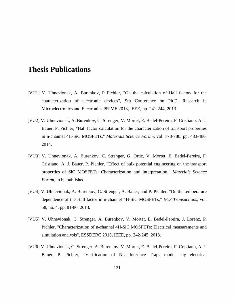
131
Thesis Publications
[VU1] V. Uhnevionak, A. Burenkov, P. Pichler, "On the calculation of Hall factors for the
characterization of electronic devices", 9th Conference on Ph.D. Research in
Microelectronics and Electronics PRIME 2013, IEEE, pp. 241-244, 2013.
[VU2] V. Uhnevionak, A. Burenkov, C. Strenger, V. Mortet, E. Bedel-Pereira, F. Cristiano, A. J.
Bauer, P. Pichler, "Hall factor calculation for the characterization of transport properties
in n-channel 4H-SiC MOSFETs," Materials Science Forum, vol. 778-780, pp. 483-486,
2014.
[VU3] V. Uhnevionak, A. Burenkov, C. Strenger, G. Ortiz, V. Mortet, E. Bedel-Pereira, F.
Cristiano, A. J. Bauer, P. Pichler, "Effect of bulk potential engineering on the transport
properties of SiC MOSFETs: Characterization and interpretation," Materials Science
Forum, to be published.
[VU4] V. Uhnevionak, A. Burenkov, C. Strenger, A. Bauer, and P. Pichler, "On the temperature
dependence of the Hall factor in n-channel 4H-SiC MOSFETs," ECS Transactions, vol.
58, no. 4, pp. 81-86, 2013.
[VU5] V. Uhnevionak, C. Strenger, A. Burenkov, V. Mortet, E. Bedel-Pereira, J. Lorenz, P.
Pichler, "Characterization of n-channel 4H-SiC MOSFETs: Electrical measurements and
simulation analysis", ESSDERC 2013, IEEE, pp. 242-245, 2013.
[VU6] V. Uhnevionak, C. Strenger, A. Burenkov, V. Mortet, E. Bedel-Pereira, F. Cristiano, A. J.
Bauer, P. Pichler, "Verification of Near-Interface Traps models by electrical
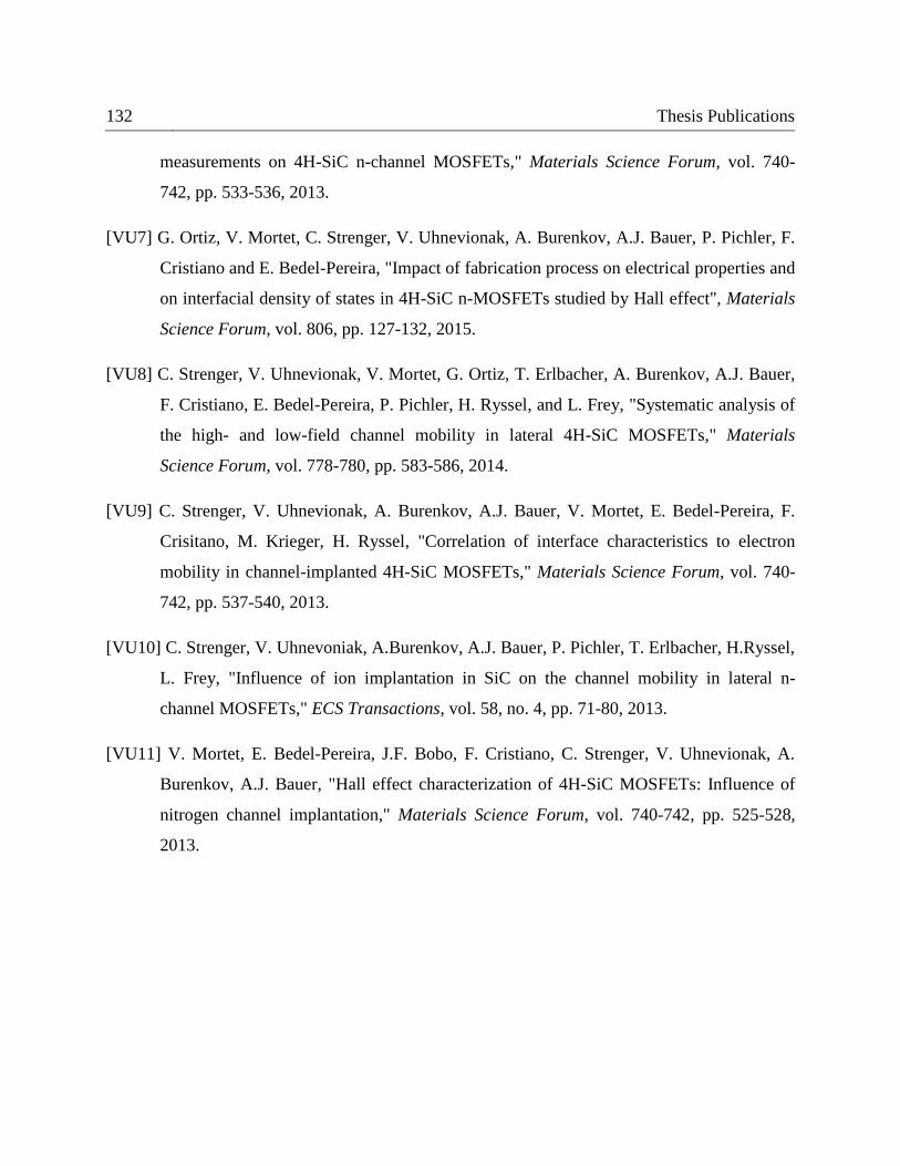
132 Thesis Publications
measurements on 4H-SiC n-channel MOSFETs," Materials Science Forum, vol. 740-
742, pp. 533-536, 2013.
[VU7] G. Ortiz, V. Mortet, C. Strenger, V. Uhnevionak, A. Burenkov, A.J. Bauer, P. Pichler, F.
Cristiano and E. Bedel-Pereira, "Impact of fabrication process on electrical properties and
on interfacial density of states in 4H-SiC n-MOSFETs studied by Hall effect", Materials
Science Forum, vol. 806, pp. 127-132, 2015.
[VU8] C. Strenger, V. Uhnevionak, V. Mortet, G. Ortiz, T. Erlbacher, A. Burenkov, A.J. Bauer,
F. Cristiano, E. Bedel-Pereira, P. Pichler, H. Ryssel, and L. Frey, "Systematic analysis of
the high- and low-field channel mobility in lateral 4H-SiC MOSFETs," Materials
Science Forum, vol. 778-780, pp. 583-586, 2014.
[VU9] C. Strenger, V. Uhnevionak, A. Burenkov, A.J. Bauer, V. Mortet, E. Bedel-Pereira, F.
Crisitano, M. Krieger, H. Ryssel, "Correlation of interface characteristics to electron
mobility in channel-implanted 4H-SiC MOSFETs," Materials Science Forum, vol. 740-
742, pp. 537-540, 2013.
[VU10] C. Strenger, V. Uhnevoniak, A.Burenkov, A.J. Bauer, P. Pichler, T. Erlbacher, H.Ryssel,
L. Frey, "Influence of ion implantation in SiC on the channel mobility in lateral n-
channel MOSFETs," ECS Transactions, vol. 58, no. 4, pp. 71-80, 2013.
[VU11] V. Mortet, E. Bedel-Pereira, J.F. Bobo, F. Cristiano, C. Strenger, V. Uhnevionak, A.
Burenkov, A.J. Bauer, "Hall effect characterization of 4H-SiC MOSFETs: Influence of
nitrogen channel implantation," Materials Science Forum, vol. 740-742, pp. 525-528,
2013.
133
List of Figures
Fig. 1 Schematic representation of the abilities of device simulation and modeling. .................... 5
Fig. 2 Diagram with the setup of device simulation. ........................................................................
Fig. 3 Top view of the Hall-Bar structure [31]. ............................................................................ 15
Fig. 4 Schematic representation of Fermi-Dirac distribution. ...................................................... 18
Fig. 5 Bandgap energy of 4H-SiC as a function of temperature. .................................................. 20
Fig. 6 Comparison of the percentage of the ionized Al atoms calculated with and without the
inclusion of doping dependence of the ionization energy. ........................................................... 22
Fig.7 Percentage of ionized Al atoms as a function of temperature for different doping
concentrations in bulk-SiC. ........................................................................................................... 23
Fig. 8 Ionized doping concentration as a function of depth at different gate voltages applied to n-
channel SiC MOSFET with NA = 5·1017
cm-3
. .............................................................................. 24
Fig. 9 Ionized doping concentration as a function of depth at VG = 0 V applied to n-channel SiC
MOSFET with NA = 5·1017
cm-3
and different concentrations QF of fixed charge. ...................... 25
Fig. 10 Oxide and interface charges in thermally grown SiO2 [41]. ............................................. 27
Fig. 11 Change of charge state of traps in dependence on the Fermi level. ................................. 28
Fig. 12 Impact of acceptor traps on the current-voltage characteristics of SiC MOSFETs. The
acceptor traps have been simulated with a concentration of 2·1012
cm-2
and a level of 50 meV
below EC........................................................................................................................................ 29
Fig. 13 Impact of positive fixed charges (left) and donor traps (right) on the current-voltage
characteristics of SiC MOSFET. The donor traps have been simulated with a concentration of
2·1012
cm-2
and a level of 50 meV below EC. ............................................................................... 30
134 List of Figures
Fig. 14 Acceptor trap distributions modeled with 𝐷𝐼𝑇𝑚𝑖𝑑 =2.4·10
11 cm
-2eV
-1, 𝐷𝐼𝑇
𝑒𝑑𝑔𝑒 =
4.6·1013
cm-2
eV-1
. The parameter σ was varied as 0.047 eV, 0.067 eV, 0.087 eV. .................... 31
Fig. 15 Diagram of optimization for density of the interface traps DIT (ET) extracted from Hall-
effect and capacitance-voltage measurements. ............................................................................. 34
Fig. 16 DIT (ET) distributions used in the simulations of the studied MOSFETs. ......................... 35
Fig. 17 Illustration of the method of DIT (ET) extraction from Hall-effect measurements. The
figure is adjusted from reference [46]. .......................................................................................... 44
Fig. 18 Interface trap density extracted from Hall-effect measurements. The Hall factor rH was
assumed to be unity in the calculation. ......................................................................................... 45
Fig. 19 Influence of Hall factor on the energetic profile of interface trap density extracted from
the Hall-effect measurements. ...................................................................................................... 46
Fig. 20 Capacitor circuit of MOS capacitor with the interface traps. The figure is adjusted from
[62]. ............................................................................................................................................... 48
Fig. 21 Capacitance circuits at low (left) and high (right) frequencies. The figure is adjusted from
[62]. ............................................................................................................................................... 49
Fig. 22 Interface trap density extracted by the high-low frequency method. ............................... 51
Fig. 23 Interface trap density extracted from C-V and Hall-effect measurements. ...................... 52
Fig. 24 Bulk mobility as a function of phosphorus concentration [VU1]. ................................... 61
Fig. 25 Dependence of the power index s for Coulomb scattering on dopant density including
screening [VU1]. ........................................................................................................................... 63
Fig. 26 Hall factor for electrons against phosphorus doping concentration in silicon [VU1]. ..... 64
Fig. 27 Comparison of default simulations and measurements for the MOSFET #E1. ............... 67
Fig. 28 Nitrogen profile measured by secondary ion mass spectroscopy. .................................... 68
Fig. 29 Comparison between the simulated and measured current-voltage characteristics. The
simulations have been performed assuming an ideal interface (solid line) and with the NIT but
without mobility degradation models (dashed line)...................................................................... 70
Fig. 30 Simulated nitrogen profile resulting in the “Nitrogen distribution” ID(VG) curve shown in
Fig. 31. .......................................................................................................................................... 71
List of Figures 135
Fig. 31 Comparison of the current-voltage characteristics simulated either with the donor trap
level or with a nitrogen profile...................................................................................................... 71
Fig. 32 Donor trap density as a function of trap energy calculated for the nitrogen profile shown
in Fig. 30. ...................................................................................................................................... 72
Fig. 33 Comparison of the drain currents simulated with a single donor trap level, with a nitrogen
profile or with a band of donor traps. ........................................................................................... 73
Fig. 34 Comparison of current-voltage characteristics simulated with NIT and mobility
degradation models with the measurements for the MOSFET #E1. ............................................ 74
Fig. 35 Comparison of the total mobility in the channel of the MOSFET #E1 calculated from the
simulated current-voltage measurements and from the mobility components using Matthiessen’s
rule. The mobility components have been obtained using the method of small variations. ......... 79
Fig. 36 Inverse mobility components in comparison to the inverse total mobility for the
MOSFET #E1. .............................................................................................................................. 80
Fig. 37 Hall factor as a function of gate voltage in the channel of the MOSFET #E1 [VU2]. .... 81
Fig. 38 Mobility components associated with Coulomb scattering at the interface charges and
surface-roughness scattering in comparison to the total mobility for the MOSFET #E1. ............ 82
Fig. 39 Sheet carrier density as a function of gate voltage in the channel of MOSFET #E1. ...... 83
Fig. 40 Drift mobility as a function of gate voltage in the channel of MOSFET #E1. ................. 83
Fig. 41 Comparison of the simulated (lines) and measured (symbols) current-voltage
characteristics [VU3]. ................................................................................................................... 86
Fig. 42 Hall factor in the channel of SiC MOSFETs with different background doping
concentrations [VU3]. ................................................................................................................... 86
Fig. 43 Doping dependence of the simualted (lines) and measured (symbols) sheet carrier
density. .......................................................................................................................................... 87
Fig. 44 Doping dependence of the simulated (lines) and measured (symbols) drift mobility. .... 87
Fig. 45 Comparison of the DIT (ET) distributions used in the simulations of the MOSFETs #E2,
#W1 and #W2 and the DIT (ET) distribution extracted from C-V measurements. ........................ 88
Fig. 46 Density of traps obtained by averaging of the DIT (ET) distributions, shown in Fig. 45. . 90
136 List of Figures
Fig. 47 Sheet carrier density for the MOSFETs with different NA simulated with the assumption
of an ideal interface (left) and with the averaged DIT (ET) distribution (right). ............................ 90
Fig. 48 Band diagram with the traps located at the interface and in the depletion width [92]. .... 91
Fig. 49 Effective channel thickness for n-channel MOSFETs with different backround doping
concentrations. .............................................................................................................................. 93
Fig. 50 Band diagrams for n-channel MOSFETs with a) NA = 5·1016
cm-3
b) NA = 1·1016
cm-3
and
c) NA = 1·1015
cm-3
[VU3]. ............................................................................................................ 94
Fig. 51 Mobility components in the channel of 4H-SiC MOSFETs with a) NA = 5·1016
cm-3
b) NA = 1·1016
cm-3
c) NA = 1·1015
cm-3
. ........................................................................................ 97
Fig. 52 Mobility component associated with Coulomb scattering at the interface (𝜇C) in the
channel of SiC MOSFETs with different background doping concentrations. ............................ 98
Fig. 53 Current-voltage characteristics for the MOSFETs #E1 (left) [VU4] and for the MOSFET
#E2 (right). Lines represent the simulations, symbols measurements. ....................................... 100
Fig. 54 Current-voltage characteristics of the MOSFET #E2, simulated with the conventional
model for 𝜇B (lines) in comparison to the measurements (symbols)........................................... 102
Fig. 55 Current-voltage characteristics of the MOSFET #E2, simulated with the conventional
model for 𝜇B at 500 K, 600 K and 700 K. ................................................................................... 102
Fig. 56 Comparison of the mobility component associated with bulk-phonon scattering
calculated using the conventional and new models. ................................................................... 103
Fig. 57 Mobility component associated with Coulomb scattering at the ionized impurities,
calculated from the conventional model. .................................................................................... 105
Fig. 58 Mobility components associated with Coulomb scattering at the ionized impurities (𝜇IMP)
and bulk-phonon scattering (𝜇BP), calculated using the new model. .......................................... 106
Fig. 59 Temperature dependence of the Hall factor in the channel of SiC MOSFET #E1 with
NA = 5·1017
cm-3
(left) [VU4] and of the MOSFET #E2 with NA = 1·1015
cm-3
(right). ............ 107
Fig. 60 Temperature dependence of the simulated (lines) and measured (symbols) sheet carrier
density in n-channel SiC MOSFETs #E1 (left) [VU4] and #E2 (right). .................................... 108
List of Figures 137
Fig. 61 Temperature dependence of the simulated (lines) and measured (symbols) drift mobility
in n-channel SiC MOSFETs #E1 (left) [VU4] and #E2 (right). ................................................. 108
Fig. 62 Mobility components associated with Coulomb scattering at the interface charges (𝜇C),
surface-phonon (𝜇SP) and bulk-phonon (𝜇BP) scattering at 300 K and 400 K for the MOSFETs
with NA equal to 5·1017
cm-3
and 1·1015
cm-3
. ............................................................................ 110

139
List of Tables
Table 1. Material properties of 4H-SiC and Si [1] .......................................................................... 2
Table 2. Doping concentrations and oxide thicknesses for the investigated MOSFETs .............. 14
Table 3. Concentration of fixed charge used in the simulations ................................................... 35
Table 4. Parameter values for bulk mobility component (𝜇B) ...................................................... 37
Table 5. Parameter values of ntrans adjusted in the model for Coulomb scattering at the interface
charges .......................................................................................................................................... 38
Table 6. Parameter values for the surface-roughness mobility component (𝜇SR) ......................... 39
Table 7. Parameter values for the surface-phonon mobility component (𝜇SP) ............................. 40
Table 8. Parameterization of the extended NIT models used in the simulations .......................... 70


141
List of Symbols
Symbol
Description Unit
B Magnetic field T
Cox Gate oxide capacitance F
CD Capacitance of depletion width F
Dn Electron diffusion coefficient cm2/s
Dp Hole diffusion coefficient cm2/s
E Energy eV
EA Ionization energy for acceptor impurity eV
ED Ionization energy for donor impurity eV
EC Conduction band energy eV
EG Bandgap energy eV
ET Trap energy eV
EV Valence band energy eV
EF Fermi energy eV
EF,n Quasi-Fermi energy for electrons eV
EF,p Quasi-Fermi energy for holes eV
Ɛ Electric field V/cm
Ɛ EFF Effective electric field V/cm
Ɛ⟘ Normal electric field V/cm
ħ Dirac constant Js
ID Drain current A

142 List of Symbols
Jn Electron current density A/cm2
Jp Hole current density A/cm2
kB Boltzmann constant J/K
L Channel length 𝜇m
𝑚𝑒∗ Effective electron mass kg
m⟘ Electron mass perpendicular to the oxide/semiconductor
interface
kg
NA Acceptor concentration cm-3
NC Effective density of states in conduction band cm-3
ND Donor concentration cm-3
Ntot Total doping concentration cm-3
NV Effective density of states in valence band cm-3
n Electron concentration cm-3
ni Intrinsic charge carrier concentration cm-3
ninv Sheet carrier density in inversion channel cm-2
p Hole concentration cm-3
QF Fixed charge charge/cm2
QIT Charge of interface traps charge/cm2
QS Space charge charge/cm2
q Elementary charge C
rH Hall factor
T Absolute temperature K
VD Drain voltage V
VG Gate voltage V
VH Hall-effect voltage V
VTH Threshold voltage V
W Channel width 𝜇m
xD Depletion width 𝜇m
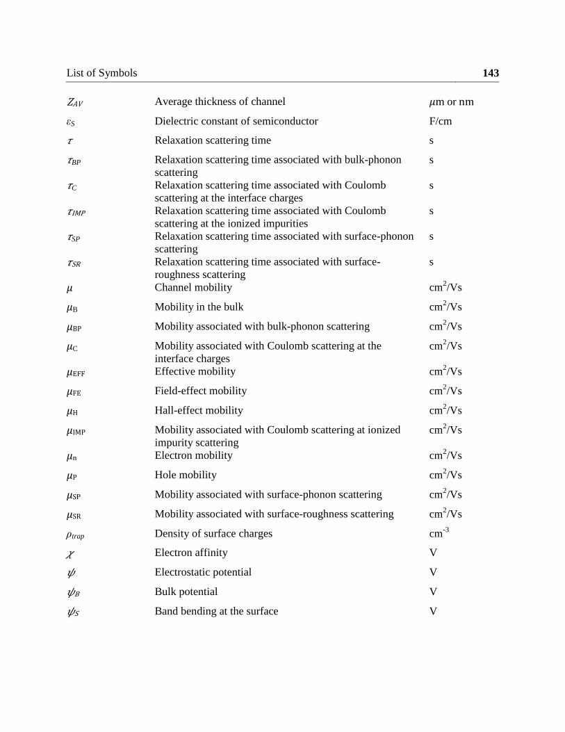
List of Symbols 143
ZAV Average thickness of channel 𝜇m or nm
εS Dielectric constant of semiconductor F/cm
𝜏 Relaxation scattering time s
𝜏BP Relaxation scattering time associated with bulk-phonon
scattering
s
𝜏C Relaxation scattering time associated with Coulomb
scattering at the interface charges
s
𝜏IMP Relaxation scattering time associated with Coulomb
scattering at the ionized impurities
s
𝜏SP Relaxation scattering time associated with surface-phonon
scattering
s
𝜏SR Relaxation scattering time associated with surface-
roughness scattering
s
𝜇 Channel mobility cm2/Vs
𝜇B Mobility in the bulk cm2/Vs
𝜇BP Mobility associated with bulk-phonon scattering cm2/Vs
𝜇C Mobility associated with Coulomb scattering at the
interface charges
cm2/Vs
𝜇EFF Effective mobility cm2/Vs
𝜇FE Field-effect mobility cm2/Vs
𝜇H Hall-effect mobility cm2/Vs
𝜇IMP Mobility associated with Coulomb scattering at ionized
impurity scattering
cm2/Vs
𝜇n Electron mobility cm2/Vs
𝜇P Hole mobility cm2/Vs
𝜇SP Mobility associated with surface-phonon scattering cm2/Vs
𝜇SR Mobility associated with surface-roughness scattering cm2/Vs
ρtrap Density of surface charges cm-3
𝜒 Electron affinity V
𝜓 Electrostatic potential V
𝜓B Bulk potential V
𝜓S Band bending at the surface V

145
Index
A
Acceptor traps ............. 28, 29, 31, 67, 71, 85
B
Band-bending .......................... 42, 47, 50, 84
Bandgap energy .............................. 6, 19, 20
Bulk potential……… 10, 42, 84, 93, 99, 100
Bulk traps .......................... 91, 92, 95, 96, 98
D
Debye length ....................................... 42, 43
Depletion width ...................... 91, 93, 95, 96
Device simulation ..................... 4, 11, 17, 20
Diffusion coefficients................................ 13
Donor traps...... 28, 30, 66, 68, 69, 71, 75, 85
E
Effective field............................................ 92
Effective mobility ............................... 75, 76
Effective thickness of channel .................. 92
Electrostatic potential................................ 12
F
Fermi integral ............................................ 19
Fermi level ................... 18, 23, 28, 30, 41,47
Fermi-Dirac statistic.................. 9, 18, 19, 47
Field-effect mobility ................... 7, 8, 75, 76
Fixed charge….25, 27, 30, 35, 43, 68, 69, 75
H
Hall factor………15, 33, 46, 55, 56, 59, 60,
61, 64, 76, 81, 86, 107, 108
Hall mass factor ............................ 59, 60, 81
Hall-Bar structures .............................. 14, 15
High-low frequency method ......... 47, 48, 50
I
Incomplete ionization................ 9, 21, 23, 26
Interface trapped charges ........ 27, 31, 41, 43
ITRS ............................................................ 4
M
Matthiessen’s rule ........... 36, 78, 79, 80, 104
Mobile ion charges .................................... 26
Mobility degradation ... 9, 67, 70, 74, 85, 100
146 Index
Mott transition ........................................... 62
N
Newton’s iterative method ........................ 13
NIT model ............. 31, 32, 68, 69, 70, 74, 85
Nitridation ............................. 3, 7, 65, 66, 75
Nitrogen distribution ..................... 69, 72, 73
NITs ............................................ 6, 7, 27, 32
Numerical optimization ...................... 32, 33
O
Oxide trapped charges............................... 27
P
Poisson equation ....................................... 12
S
Scattering relaxation time ................... 76, 77
SIMS ................................................... 68, 69
Step-controlled epitaxy ............................. 38
T
TCAD ................................ 4, 5, 6, 60, 77, 78
Threshold voltage.... 8, 26, 29, 30, 67, 70, 72
W
WBG semiconductors ............................. 1, 2