Embed Size (px)
Citation preview
Simulating Charge Stability Diagrams for Double and Triple
Quantum Dot Systems
Ian E. Powell
(Dated: September 2, 2014)
Abstract
We recreate Sandia National Laboratories’ double quantum dot charge stability diagram simu-
lation using their rate equation approach and compare our simulation’s results to some touchstone
situations as well as their results. We find qualitative agreement between charge stability diagrams
and extend the code to construct the charge stability diagram for a triple dot structure. We note
how the triple dot charge stability diagrams change as the third gate voltage is increased.
1

I. INTRODUCTION
A. Quantum Computing in Solid State Quantum Dots
The field of quantum computing has received a great deal of attention in the physics com-
munity due to its exciting prospective applications and recent progress made in constructing
systems with characteristics that allow for the formation of so called “qubits.” A qubit, short
for quantum bit, represents a two-level, quantum mechanical system. Canonical examples
of a qubit are a photon’s polarization–be it linearly horizontal or linearly vertical–or an
electron’s spin state–where down and up, or horizontal and vertical correspond to 0 and 1
in terms of binary. The difference, between a qubit and a classical bit is the qubit’s ability
to be in both 0 and 1 simultaneously–a superposition of up and down for the example of the
electron’s spin. It is this property of superposition, along with something called quantum
entanglement, that differentiates quantum computing from its classical counterpart.
David Divincezo of IBM famously constructed a list of requirements to construct quantum
computer. The “DiVincenzo Criteria” are: (1) the system must have a large number of well
defined qubits, (2) initialization to a known state for the system must be easily performed,
(3) a universal set of quantum logic gates must be developed, (4) qubit-specific measurements
must be able to be performed, (5) and long coherence times must exist for the qubits in
the system1–where coherence time describes how long a quantum state can exist on average
before being perturbed, and, in turn, altered by the environment.
Many different types of systems show promise in fulfilling said criteria–for example, super-
conducting systems have shown promise in quantum information processing due to the ease
of fabricating larger systems. Cold neutral atom systems’ qubits have some of the longest co-
herence times–offering promise for storing information for longer periods of time. Solid-state
systems in which spin states of electrons or nuclei represent the qubits have serious promise
in their scalability, due to extensive research done on the miniaturizing of semiconductors
for computing. This summer I worked on researching a solid state system–namely quantum
dots–for quantum computing purposes.
A quantum dot is generally any 3-D potential well, but in the context of solid-state
physics it is a structure made of semiconducting material that is small enough to exhibit
quantum mechanical phenomena. The dot’s bound states of electron and electron-hole, or
2
excitons, are confined in all three spatial dimensions. The electronic properties of a single
dot, its discrete energy levels etc., are akin to that of an atom–hence the nickname for a
quantum dot is “artificial atom.” When another dot is introduced into the system and there
exists a strong, coherent, in-phase tunneling of electrons between the two dots, the system
behaves similar to a covalently bonded molecule.
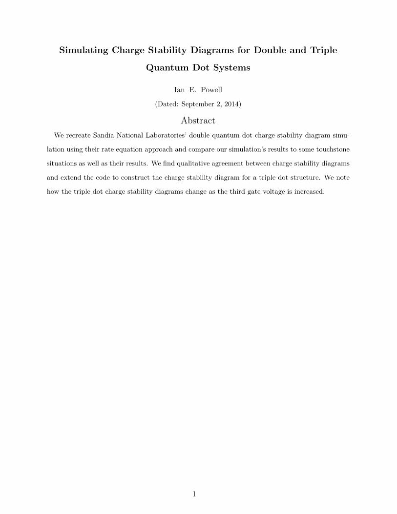
We utilize double and triple quantum dots which have been fashioned onto a Si-SiO2
heterostructure as our means for quantum computing; for a schematic of a GaAs-AlGaAs
heterostructure see Fig. I.
FIG. 1. Schematic of a GaAs-AlGaAs heterostructure taken from [2].
At the interface between the two different materials a two dimensional electron gas (2DEG)
forms. To further confine the other two dimensions of motion we apply voltages to the
gates to create potential wells and trap some target number of electrons. We utilize a
quantum point contact (QPC) to determine the current through the dots and, in turn, the
occupancy of each dot. This is due to the fact that the QPC has a systematically varying
conductance as the occupation of the dots varies. The QPC, as opposed to some ammeter,
has the advantage of measuring the current of electrons through the dots indirectly–thereby
not perturbing our system of qubits, and thus not destroying any information stored in our
system.
There are two different types of qubits that are viable for double dot systems–spin qubits
and charge qubits. The bases for a double dot system’s spin qubits are the singlet and triplet
states–i.e. (S = 0, Sz = 0) = |0〉, (S = 1, Sz = 0) = |1〉. The bases for the charge qubits are
based on electron occupation of the dots–for example (0,1) occupancy could be |0〉 whereas
3

(1,0) would be |1〉–for a helpful visualization of the wave function of our system written in
terms of our qubit bases see Fig. II. For the triple dot system we utilize the Heisenberg
FIG. 2. The “Bloch Sphere” visualization of a qubit’s wave function.
interaction and the “singlet” and “triplet-like” states as our bases–where, for example, |0〉
= |S〉 |↑〉, |1〉 = (2/3)1/2 |T+〉 |↓〉 - (1/3)1/2 |T0〉 |↑〉3.
For a given dot structure a charge stability diagram, or a “honeycomb diagram,” can be
formed–telling us at which gate voltages what electron occupancy is favored. To construct
this diagram we first model our double or triple dot as a system of capacitors and then follow
a rate-equation approach developed by a group working at Sandia National Laboratories
highlighted in the next section. Honeycomb diagrams have very distinct characteristics for
different sets of system parameters. For example, in a perfectly uncoupled double dot–in
the sense that the mutual capacitance between the dots → 0–we would expect a pattern of
rectangles to be formed in our stability plot. In a perfectly coupled system such that the
capacitance of each dot equals the mutual capacitance we would expect rectangles again,
however, now they would be symmetric about the Vg1 = Vg2 line where Vg1(g2) is the gate
voltage on dot 1(2)–for a visualization of these stability diagrams see Fig. III. We recreate
these figures–(a) → (c)–and others shown in Sandia National Laboratories’ paper4 to show
that we have successfully recreated Sandia’s simulation and continue to discuss how we
extended it for use in a triple dot system.
4

FIG. 3. Different honeycomb diagrams for select cases of system parameters taken from [5].
B. Sandia’s Paper
The Paper written by Sandia Nation laboratories which we follow discusses a double
quantum dot structure that they extract biasing triangles from–structures that form in hon-
eycomb diagrams when a biasing voltage is present–and model using their rate equation
approach. With this model they can identify how different tunneling imbalances and tem-
peratures affect a charge stability diagram–namely how edges may be obfuscated or shifted.
Some of the figures from their paper are shown in the Results section below–highlighting
how different relative tunneling rates can alter the honeycomb diagram significantly.
5
II. THEORY
A. Energy Of a Double Dot
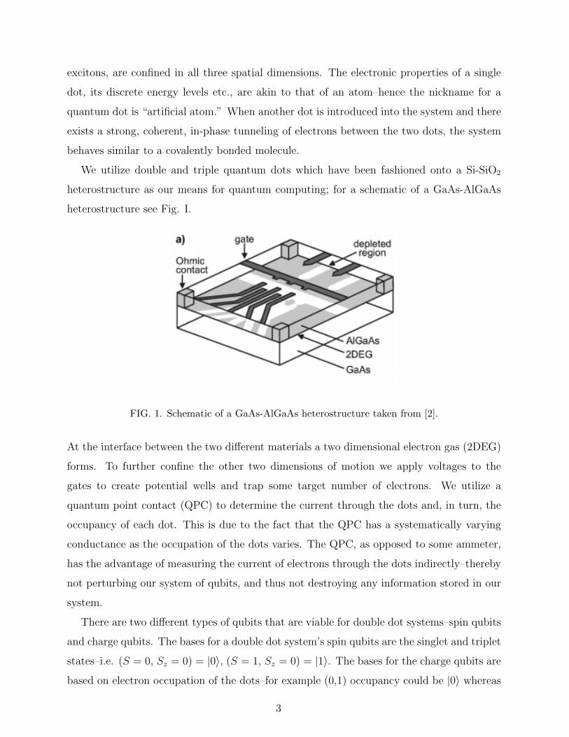
The energy of a double dot modeled by a system of capacitors is
U =1
2~V ·C~V , (1)
where ~V is the voltage vector and C is the capacitance matrix. To find ~V we write the total
charge in each dot as the charge accumulated on each capacitor connected to the dot
Q1 = CL(V1 − VL) + Cg1(V1 − Vg1) + Cm(V1 − V2) + Cg21(V1 − Vg2) (2)
Q2 = CR(V2 − VR) + Cg2(V2 − Vg2) + Cm(V2 − V1) + Cg12(V2 − Vg1), (3)
where Q1(2) is the charge on dot 1(2), V1(2) is the voltage of dot 1(2), C1(2) is the capacitance
of dot 1(2), Cm is the mutual capacitance between dots, VL − VR is the bias voltage across
the system, and Cg21(g12) is the cross capacitance between gate 2(1) and dot 1(2)–for a circuit
diagram of the system see Fig. IV. We rewrite this in terms of the capacitance matrix and
FIG. 4. Capacitor model for a double dot with cross-gate capacitances.
voltage vector Q1 + CLVL + Cg1Vg1 + Cg21Vg2
Q2 + CRVR + Cg2Vg2 + Cg12Vg1
= C
V1
V2
, (4)
where
C =
C1 −Cm
−Cm C2
. (5)
6

We now invert our capacitance matrix, and write our charge in terms of the occupancy of
each dot–N1(2), with Q1(2) = −|e|N1(2)–to find our voltage vector in terms of our capacitances V1
V2
=1
C1C2 − C2m
C2 Cm
Cm C1
× −|e|N1 + CLVL + Cg1Vg1 + Cg21Vg2
−|e|N2 + CRVR + Cg2Vg2 + Cg12Vg1
. (6)
We rewrite Equation (1) as
U =1
2C1V
21 +
1
2C2V
22 − CmV1V2, (7)
and plug in our values of V1 and V2 found using Equation (6) to find the electrochemical
potential of our double dot system.
B. Energy Of a Triple Dot
We model our triple dot as a system of capacitors as we did with our double dot–see Fig.
V. Accounting for our charge as we did with the double dot we yield
FIG. 5. Capacitor model for a double dot with cross-gate capacitances.
Q1 + CLVL + Cg1Vg1 + Cg21Vg2
Q2 + Cg2Vg2 + Cg12Vg1 + Cg32Vg3
Q3 + CRVR + Cg3Vg3 + Cg23Vg2
= C
V1
V2
V3
, (8)
where our capacitance matrix is now given by
C =
C1 −Cm1 0
−Cm1 C2 −Cm2
0 −Cm2 C3
. (9)
7

We invert our capacitance matrix to find ~V as we did with the double dot, and utilize
Equation (1) to find our electrochemical potential expression
U =1
2C1V
21 +
1
2C2V
22 +
1
2C3V
23 − Cm1V1V2 − Cm2V2V3. (10)
We do assume in our model that there is negligible coupling between dots 1 and 3; this is
a reasonable assumption for some structures but not all. In the case that the coupling isn’t
negligible we would add terms to the capacitance matrix in Equation (9) and the charging
terms in Equation (8) as necessary.
C. Rate Equation Approach
To construct the charge stability diagram of a double or triple dot we utilize a rate
equation approach as highlighted in Sandia National Labs’ Paper.
For a dot system in state a we write the transition amplitude from state a to state b as
Γab = tabf(U(a)− U(b)), (11)
where tab is the tunneling rate between state a and state b, f is the Fermi-Dirac distribution
function, and U is the electrochemical potential of the system. For our simulation we consider
only single electron transitions between state a to b.
To understand how the probability of being in state a, Pa, changes with respect to time
we construct the rate equation
dPa
dt=
∑k 6=a
ΓkaPk −∑k
ΓakPa. (12)
The positive term accounts for all ways our system in some other state k may transition to
state a, and the negative term accounts for all ways our system in state a may transition to
some other state k in a time step dt. To find the steady-state solution we set Equation (9)
equal to 0 and construct the matrix equation
M~P = 0, where Mab =
Γba, a 6= b
−∑
k Γak, a = b,(13)
thus our probability vector, ~P , can be found by finding the nullspace of our M matrix.
8

We then find the average occupancy of our dots via the weighted sum
N̄ =∑k
PkNk, (14)
where Nk is the number of electrons in each dot in state k. To visualize our charge stability
diagram we then take the total derivative of our occupancy with respect to our gate voltages
and make a grey-scale contour plot. Alternatively we can also visualize the honeycomb by
plotting the probabilities where they are ≈ .5.
D. The Algorithm
For the algorithm, we chose to iterate over situations where the system state can go from
a to b via a single electron. We construct a n × n matrix where n = number of states the
system can be in with a maximum number of electrons present. Utilizing a bit of statistics
we find that n = (N ′ + E)!/(E!N ′!), where N ′ is the number of dots in our system, and E
is the allowed maximum number of electrons in our system.
The algorithm goes as the following:
Iterating over the gate voltages, we choose an initial occupancy and find the transition
amplitudes from that state to all other states; we store these transition amplitudes in our
n×n matrix and repeat this for all other possible occupancies thereby yielding the probability
vector ~P–via the null space of this M–and thus the occupation associated with the system
associated with the gate voltage configuration. We store each probability vector and each
dot occupation for each voltage configuration until we have iterated over all chosen gate
voltages. The code for the double dot simulation can be found in The Appendix.
9

III. RESULTS
A. Double Dot
We first recreate Fig. III (a) and (b) with arbitrary parameters and units using 3600
pixels in each plot shown–see Fig. VI and VII.
FIG. 6. Perfectly uncoupled system with a maximum of two electrons.
FIG. 7. Imperfectly coupled system with a maximum of three electrons.
Fig. 6 appears how we would expect it to–the diagonal line that separates the (1,1) and
(0,2) states is due to the fact that there are a maximum of two electrons in the system at
one time. Fig. 7 shows a reasonable structure as well with the formation of triple dots as
seen in Fig. III (b).
10

We now recreate Sandia’s figures with their listed values, the tunneling rates between
source and left dot, left dot and right dot, and right dot and drain are listed as tL : tm : tR;
our plots’ axis are in units of volts–see Fig. VIII and Fig. IX.
FIG. 8. Simulation comparison using Sandia’s system parameters for tunneling rates 0.01 : 1 : 0.1
FIG. 9. Simulation comparison using Sandia’s system parameters with tunneling rates listed as
1 : 1 : 1.
Both our results and Sandia’s are in qualitative agreement as both exhibit similar struc-
ture, however an in depth quantitative comparison is yet to be done. One considerable
disagreement is that all of our structures are a factor of 10 larger than those in the Sandia
paper–this is likely due to a units issue that has eluded us or them.
11

B. Triple Dot
Using Sandia’s original values for the first two dots and C3 = 55 aF, Cg3 = 1.7 aF,
Cg32 = 1.1 aF, Cg23 = 1.3 aF for the third dot, with no biasing voltage present, we create
two probability plots to highlight the structural change of the honeycomb diagram as Vg3
increases from 5 mV to 10 mV. The tunneling rates between source and left dot, left dot and
middle dot, middle dot and right dot, and right dot and drain are listed as tL : tcl : tcr : tR–see
Fig. X and Fig. XI.
FIG. 10. Honeycomb Diagram at Vg3 = 5 mV and T = .15K, with tunneling rates 1 : 1 : 1 : 1
12
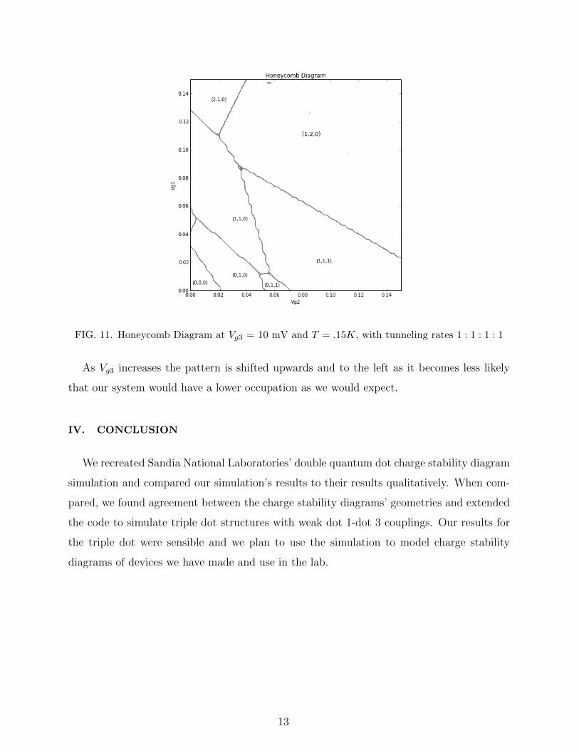
FIG. 11. Honeycomb Diagram at Vg3 = 10 mV and T = .15K, with tunneling rates 1 : 1 : 1 : 1
As Vg3 increases the pattern is shifted upwards and to the left as it becomes less likely
that our system would have a lower occupation as we would expect.
IV. CONCLUSION
We recreated Sandia National Laboratories’ double quantum dot charge stability diagram
simulation and compared our simulation’s results to their results qualitatively. When com-
pared, we found agreement between the charge stability diagrams’ geometries and extended
the code to simulate triple dot structures with weak dot 1-dot 3 couplings. Our results for
the triple dot were sensible and we plan to use the simulation to model charge stability
diagrams of devices we have made and use in the lab.
13

ACKNOWLEDGMENTS
I would like to thank Professor Hong-Wen Jiang for mentoring me while I worked on this
project during my stay at UCLA, Blake Freeman and Joshua Schoenfield for all of their
useful discussions and guidance, and the NSF.
V. APPENDIX
iterations = 40 #total iterations = iterations squared
Vg1_max=.06
Vg1_min=0.
Vg2_max=.06
Vg2_min=0.
dV=(Vg1_max-Vg1_min)/iterations
print dV
V_0=0 #initialize
#tunneling factors
tS = 1. #tunneling from source to left dot
tM = 1. #tunneling from left dot to right dot
tD = .0 #tunneling from right dot to drain
T=1e-4
#Solve linear system.
#Double Dot, 2 electrons
N1_0=0. #starting number in dot 1
N2_0=0. # starting number in dot 2
14

Vgate_1=[] #Gate voltage lists
Vgate_2=[]
elec=4. #max electrons in system
Gamma_array=np.zeros((500,500))
N_list=[] #initializing the list of states
q=0 #counter
r=0 #counter
Master_G_array=[]
for l in range(iterations+1):
for k in range(iterations+1):
q=0 #counter
#counter
N1_0=0. #starting number in dot 1
N2_0=0. # starting number in dot 2
Gamma_array=np.zeros((500,500))#initialize every iteration
inv_array=np.zeros((500,500))
for g in range(int(elec)+1):#changing configuration
for h in range(int(elec)+1):
r=0
q+=1
for i in range(int(elec)+1): #scanning over transitions for
a particular configuration
for j in range(int(elec)+1):
r+=1
# print r
if (g+h<=elec and i+j<=elec): #Avoid iterating over
situations where there are more than max electrons
15

N_list.append([g,h])
#Criteria for an acceptable transition of one electron
if (((i!=g or j!=h) and (abs(g-i)+ abs(h-j)))<=elec
and (abs(g+h-i-j)<=1)):
#Tunneling direction logic in next if statements
if (i<g and h==j):
Gamma_array[q-1][r-1]=
Gamma_out(tS,g,h,i,j,l*dV,k*dV,T)
inv_array[q-1][r-1]=
Gamma_out_inv(tS,g,h,i,j,l*dV,k*dV,T)
if (g==i and h<j):
Gamma_array[q-1][r-1]=
Gamma(tD,g,h,i,j,l*dV,k*dV,T)
inv_array[q-1][r-1]=
Gamma_inv(tD,g,h,i,j,l*dV,k*dV,T)
if (h<j and g>i):
Gamma_array[q-1[r-1]=
Gamma(tM,g,h,i,j,l*dV,k*dV,T)
inv_array[q-1][r-1]=
Gamma_inv(tM,g,h,i,j,l*dV,k*dV,T)
if (g<i and h>j):
Gamma_array[q-1][r-1]=
Gamma(tM,g,h,i,j,l*dV,k*dV,T)
inv_array[q-1][r-1]=
Gamma_inv(tM,g,h,i,j,l*dV,k*dV,T)
if (h==j and i>g):
Gamma_array[q-1][r-1]=
Gamma_in(tS,g,h,i,j,l*dV,k*dV,T)
inv_array[q-1][r-1]=
Gamma_in_inv(tS,g,h,i,j,l*dV,k*dV,T)
if (j<h and g==i):
Gamma_array[q-1][r-1]=
16

Gamma(tD,g,h,i,j,l*dV,k*dV,T)
inv_array[q-1][r-1]=
Gamma_inv(tD,g,h,i,j,l*dV,k*dV,T)
else:
None
else:
None
else:
None
if g==elec:
break
else:
None
Count_Deletes=0
#Deleting the extra trivial rows
for i in range(len(Gamma_array[0])):
if np.all(np.zeros(len(Gamma_array))-(Gamma_array[:,i-Count_Deletes])==0)
and np.all(np.zeros(len(Gamma_array))-(Gamma_array[i-Count_Deletes])==0):
Gamma_array=np.delete(Gamma_array,(i-Count_Deletes),axis=1)
#Delete Column
Gamma_array=np.delete(Gamma_array,(i-Count_Deletes),axis=0)
#Delete Row (square matrix)
inv_array=np.delete(inv_array,(i-Count_Deletes),axis=1) #Delete
Column
inv_array=np.delete(inv_array,(i-Count_Deletes),axis=0) #Delete
Row (square matrix)
Count_Deletes+=1
else:
None
17
for m in range(len(Gamma_array)):
for n in range(len(Gamma_array)):
if (m==n):
Gamma_array[m][n]+=-sum(inv_array[m])
Master_G_array.append(Gamma_array)
Vgate_1.append(l*dV+Vg1_min)
Vgate_2.append(k*dV+Vg2_min)
print l*dV
1 David P. DiVincenzo, IBM (2000-04-13). “The Physical Implementation of Quantum Computa-
tion”.
2 R. Hanson et.al., “Spins in few-electron quantum dots” Reviews of Modern Physics. 79, October-
December 2007.
3 DiVincenzo et.al., “Universal quantum computation with the exchange interaction” Letters to
Nature, 2000.
4 Khoi T. Nguyen et.al., “Charge Sensed Pauli Blockade in a Metal-Oxide-Semiconductor Lateral
Double Quantum Dot” Nano Letters. 13 75, 5785-5790, 2013.
5 W.G. van der Wiel et.al., “Electron transport through double quantum dots” Reviews of Modern
Physics. 75, January 2003.
18