Embed Size (px)
Citation preview

HOME APPLICATION NOTES
1 MICROMETALS, INC. • 5615 E. LA PALMA AVENUE • ANAHEIM, CALIFORNIA 92807-2109 • USA
SIMPLIFIED CALCULATION OF MAGNETIC AND ELECTRICAL LOSSES
IN UNITY POWER FACTOR BOOST PREREGULATORS
by:
Bruce Carsten
for:
MICROMETALS INC. 5615 E. La Palma Ave.
Anaheim, CA 92807-2109 Phone : 714-970-9400
Fax: 714-970-0400
ABSTRACT
There is an increasing demand for minimization of harmonic currents drawn from the AC mains by power supplies. For many applications in the 100 W to 10 KW range, the Unity Power Factor (UPF) boost preregulator �front end� is finding increasing use. Unfortunately the power circuit voltages, currents and switching duty cycle are continuously changing throughout the AC line cycle, even for �fixed� input and output conditions, which significantly complicates the calculation of losses in the preregulator. Formulas, graphs and rules-of-thumb are presented which simplify the calculation of most circuit losses.
INTRODUCTION
Switchmode off-line power supplies have traditionally used a bridge rectifier and capacitor input filter to convert the AC mains voltage to DC, which was then chopped, transformed, rectified and filtered at a high frequency to achieve regulated, isolated lower voltage output(s). The use of a capacitor input filter on the rectified line voltage had the advantages of relatively low cost and light weight, which assisted Switchmode supplies in displacing bulky and inefficient �linear� designs. The major drawback to the use of a capacitor input filter is that the AC input is �peak� rectified; current is drawn from the line only near the peak of the AC voltage. The resultant current waveform is rich in harmonics, which increase I2R losses in the AC mains. Only current �in phase� with the line voltage contributes to power flow; an �out of phase� fundamental component and all harmonic currents are �reactive� (i.e. circulate energy with no net power flow). This reduces the AC mains �Power Factor� (PF), defined as:
(1) Ix V
PPF =
Where: P = Power Flow
V = AC Mains RMS Voltage I = AC Mains RMS Current
There was little concern as long as switchmode supplies represented a small fraction of the total load on the power line, but this is often no longer the case. In modern office buildings the computers, copiers, FAX�s, PABX�s and even the lighting may use switchmode power converters. In North America the standard commercial power is 60Hz, 3 phase, 120/208 VAC, with the various 120 VAC wall outlets taken from the three L-N phases in turn.
MICROMETALS, INC. • 5615 E. LA PALMA AVENUE • ANAHEIM, CALIFORNIA 92807-2109 • USA
2
The major problem with capacitor input filter supplies are the large 3rd harmonic currents, which are typically 40% to 70% of the fundamental in amplitude. Balanced L-N fundamental (60Hz) currents in a 3 phase system cancel on the neutral wire, but 3rd harmonic (180 Hz) currents are additive; the relative 3rd harmonic phase shift between line phases is 3 x 120o = 360o, which are thus �in phase�. A preponderance of conventional switchmode supplies on the AC mains readily causes the neutral wire current to exceed capacity. With no overcurrent protection on the neutral, fires have resulted. The increasingly mandated solution is to improve switchmode supply Power Factors in general, and to reduce the 3rd harmonic currents in particular. There are numerous approaches to power factor enhancement, of varying complexity, cost and effectiveness. The use of a Unity Power Factor (UPF) boost preregulator with a following DC-DC converter is one of the most popular approaches, for several reasons:
1) Harmonic currents can be reduced to a few % or less (PF > 0.99);
2) Throughput power is high, relative to component stresses [1];
3) Preregulator efficiencies in the mid to high 90�s are readily achieved, so efficiency is little compromised;
4) Worst case �holdup� time is significantly improved for a given value of
bulk storage capacity;
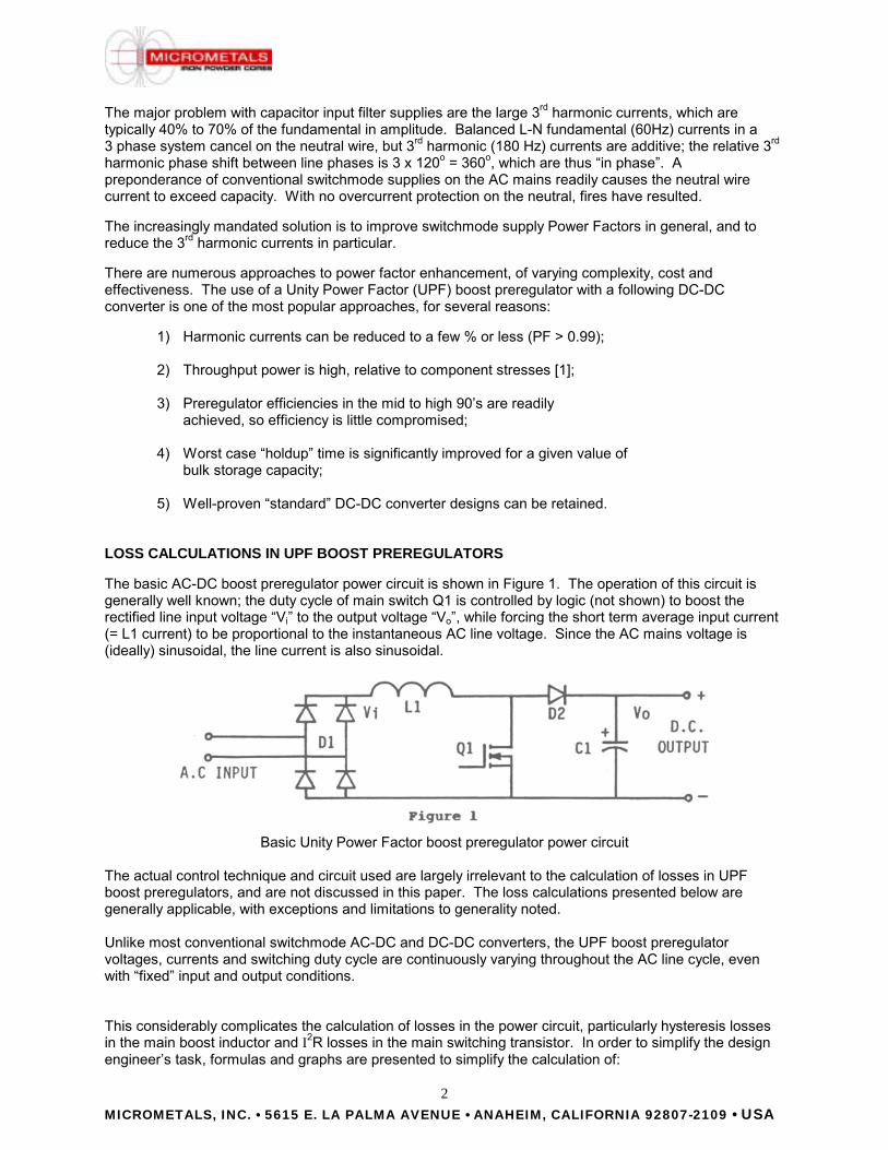
5) Well-proven �standard� DC-DC converter designs can be retained. LOSS CALCULATIONS IN UPF BOOST PREREGULATORS The basic AC-DC boost preregulator power circuit is shown in Figure 1. The operation of this circuit is generally well known; the duty cycle of main switch Q1 is controlled by logic (not shown) to boost the rectified line input voltage �Vi� to the output voltage �Vo�, while forcing the short term average input current (= L1 current) to be proportional to the instantaneous AC line voltage. Since the AC mains voltage is (ideally) sinusoidal, the line current is also sinusoidal.
Basic Unity Power Factor boost preregulator power circuit
The actual control technique and circuit used are largely irrelevant to the calculation of losses in UPF boost preregulators, and are not discussed in this paper. The loss calculations presented below are generally applicable, with exceptions and limitations to generality noted. Unlike most conventional switchmode AC-DC and DC-DC converters, the UPF boost preregulator voltages, currents and switching duty cycle are continuously varying throughout the AC line cycle, even with �fixed� input and output conditions. This considerably complicates the calculation of losses in the power circuit, particularly hysteresis losses in the main boost inductor and I2R losses in the main switching transistor. In order to simplify the design engineer�s task, formulas and graphs are presented to simplify the calculation of:

MICROMETALS, INC. • 5615 E. LA PALMA AVENUE • ANAHEIM, CALIFORNIA 92807-2109 • USA
3
1) Average HF hysteresis loss in the main inductor, for various values of magnetic flux loss exponent and operating conditions;
2) High (switching) frequency RMS currents in the inductor winding (used in calculation of HF skin and proximity effect losses);
3) Low frequency (DC and twice line frequency) RMS and Peak inductor currents
(for calculating LF conductor and hysteresis losses);
4) RMS and Peak currents in the main switching transistor;
5) RMS, peak and average currents in the main boost rectifier;
6) RMS ripple currents in the main boost filter capacitor at both power conversion and twice-line frequencies.
Most currents are normalized to the average DC output current, and plotted as a function of peak AC input/DC output voltage. Main inductor HF conductor and hysteresis losses are normalized to the readily calculated maximum values occurring when the (instantaneous) input voltage equals half the DC output voltage. Formulae are given to convert the normalized currents and losses to actual operating currents and losses. HYSTERESIS LOSSES IN THE MAIN INDUCTOR A sinusoidal input voltage, constant output voltage and constant conversion frequency are assumed for calculating the (relative) AC core and HF winding current losses in the main inductor (L1). The peak HF AC flux in the inductor core can be calculated from the switching voltage waveform. A conventional formula for peak flux � B̂ � in CGS units is:
(2) A N 2
T E 810B̂ ∆=
For convenience we "normalize" by letting:
(3) 2 / 10 AN 8= Then:
(4) T E B̂ ∆= In a boost regulator: (5) T DV T E i=∆ And:
(6) o
i
VV - 1 D =
Where: E = Inductor Voltage
∆T = Time Increments N = Number of Winding Turns A = Core Area Vi = Input Voltage
iV̂ = Peak Input Voltage Vo = DC Output Voltage D = Switch Duty Cycle F = Conversion Frequency T = 1/F
MICROMETALS, INC. • 5615 E. LA PALMA AVENUE • ANAHEIM, CALIFORNIA 92807-2109 • USA
4
Substituting (5) & (6) into (4), and letting F = 1:
(7) o
2ii
V)(V - V B̂ =
Over an AC line cycle:
(8) t)sin( V̂ V ii ω= So:
(9) t)(sin V
)V̂( - t)sin( V̂ B̂ 2
o
2ii ωω=
Or:
(10) t))cos(2 -(1 V 2)V̂( - t)sin( V̂ B̂
o
2ii ωω=
The maximum flux � B̂ max� occurs when: (11) /2V V oi = Substituting (11) into (7):
(12) /4V max B̂ o= And dividing (10) by (12):
(13) 1) - t)(cos(2 VV̂2 t)sin(
VV̂ 4 max B̂/B̂
2
o
i
o
i ωω
+=
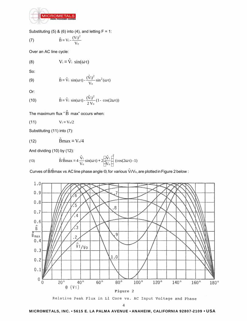
:below 2 Figure in plotted are ,/VV various for , angle phase line AC vs maxB/B of Curves oiˆˆˆ Θ
MICROMETALS, INC. • 5615 E. LA PALMA AVENUE • ANAHEIM, CALIFORNIA 92807-2109 • USA
5
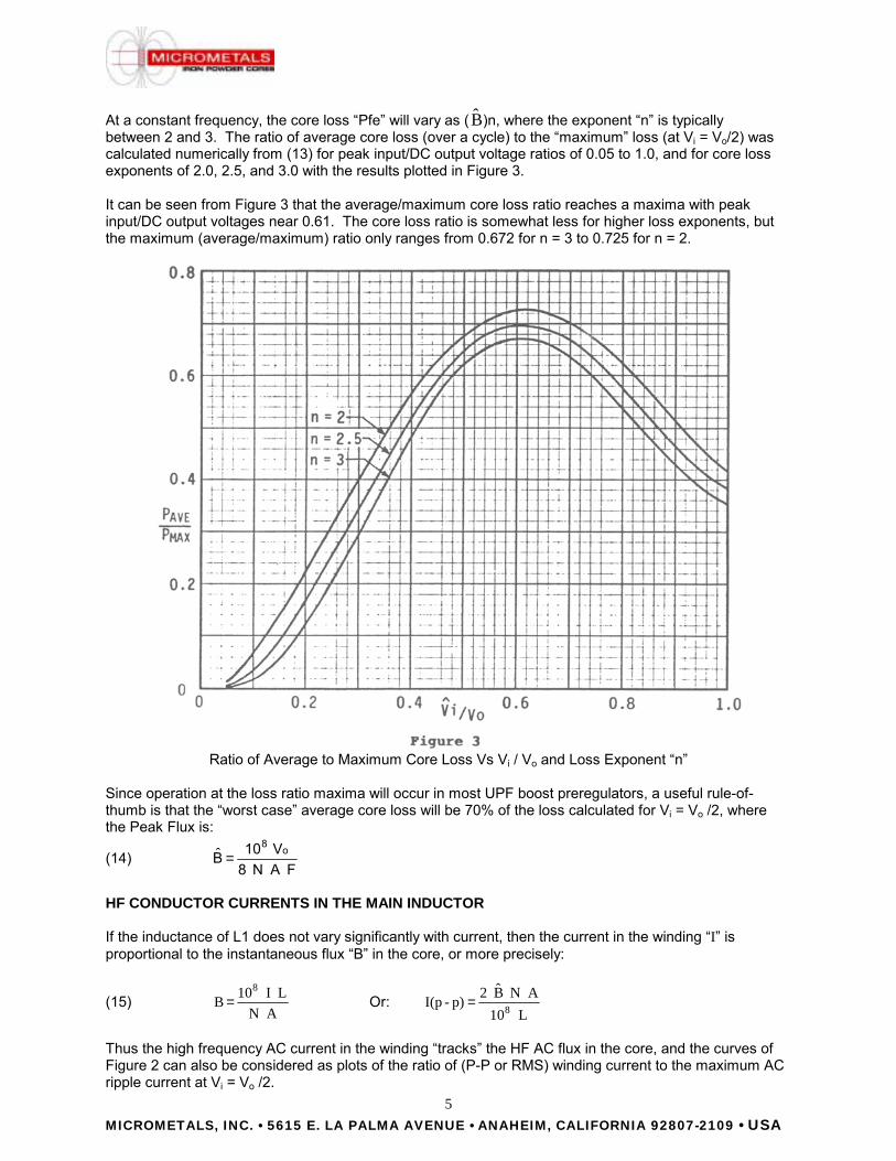
At a constant frequency, the core loss �Pfe� will vary as ( B̂)n, where the exponent �n� is typically between 2 and 3. The ratio of average core loss (over a cycle) to the �maximum� loss (at Vi = Vo/2) was calculated numerically from (13) for peak input/DC output voltage ratios of 0.05 to 1.0, and for core loss exponents of 2.0, 2.5, and 3.0 with the results plotted in Figure 3. It can be seen from Figure 3 that the average/maximum core loss ratio reaches a maxima with peak input/DC output voltages near 0.61. The core loss ratio is somewhat less for higher loss exponents, but the maximum (average/maximum) ratio only ranges from 0.672 for n = 3 to 0.725 for n = 2.
Ratio of Average to Maximum Core Loss Vs Vi / Vo and Loss Exponent �n�
Since operation at the loss ratio maxima will occur in most UPF boost preregulators, a useful rule-of-thumb is that the �worst case� average core loss will be 70% of the loss calculated for Vi = Vo /2, where the Peak Flux is:
(14) F A N 8
V10 B o 8=ˆ
HF CONDUCTOR CURRENTS IN THE MAIN INDUCTOR If the inductance of L1 does not vary significantly with current, then the current in the winding �I� is proportional to the instantaneous flux �B� in the core, or more precisely:
(15) AN LI 10 B
8= Or:
L10AN B̂ 2 p)-I(p 8=
Thus the high frequency AC current in the winding �tracks� the HF AC flux in the core, and the curves of Figure 2 can also be considered as plots of the ratio of (P-P or RMS) winding current to the maximum AC ripple current at Vi = Vo /2.

MICROMETALS, INC. • 5615 E. LA PALMA AVENUE • ANAHEIM, CALIFORNIA 92807-2109 • USA
6
Furthermore, since conductor loss varies as I2, the �n = 2� curve of Figure 3 can be used to find the �average to maximum� HF conductor loss ratio versus Vi / Vo, which (as noted) has a maximum value of 0.725. The triangular wave inductor current has a sufficiently low harmonic content that HF skin and proximity effect losses can be calculated assuming a sinusoidal current of the same RMS value:
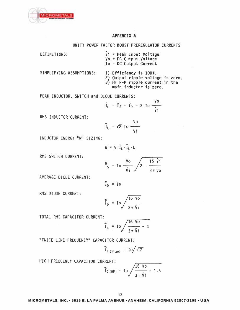
(16) 3p)/2-I(p I(rms) = The actual calculation of the HF winding losses is beyond the scope of this paper; refer to [2] through [6] for assistance. CALCULATING CURRENTS IN THE OTHER POWER COMPONENTS The derivations of peak, average and RMS currents in the other power components are a little too involved for inclusion in this paper. The formulae are tabulated in Appendix A, and plotted in the curves of Figure 4 on the next page.
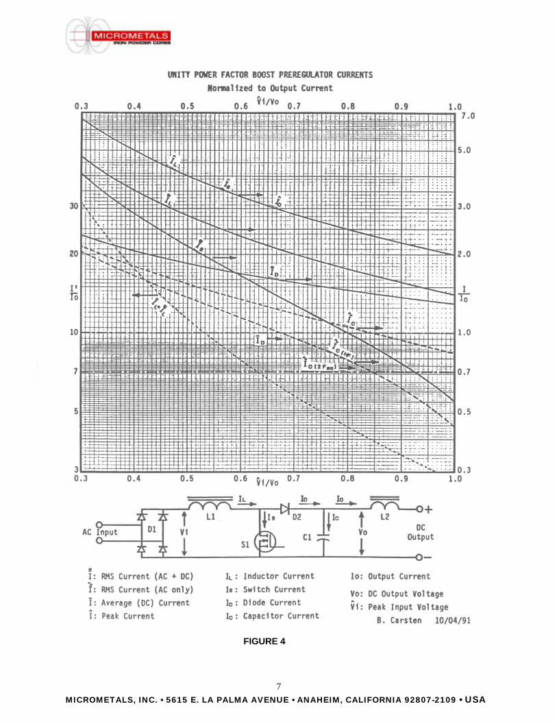
MICROMETALS, INC. • 5615 E. LA PALMA AVENUE • ANAHEIM, CALIFORNIA 92807-2109 • USA
7
FIGURE 4

MICROMETALS, INC. • 5615 E. LA PALMA AVENUE • ANAHEIM, CALIFORNIA 92807-2109 • USA
8
Component currents in Figure 4 are normalized to the DC output current �Io� and plotted as a function of the peak input/DC output voltage ratio �Vi / Vo�. An explanation of these currents and their use in loss calculations is given for the various power components. General: The graphs in Figure 4 and the formulas in Appendix A apply for any conversion frequency. The conversion frequency may vary with input voltage and current, unlike the derivations of main inductor HF winding currents and relative core loss above. The following assumptions were made in the analysis:
1) The AC input voltage is sinusoidal;
2) All components are ideal (no diode drop of switch loss);
3) The output voltage is constant (large filter capacity C1);
4) HF ripple current in the main inductor is small (L1 is large). In practice, the formulas and graphs are reasonably accurate if the P-P output ripple voltage is <10% of Vo, and the main inductor current is at or above critical current most of the time. Most of the HF RMS current in Q1, D2 and C1 is due to the pulse width modulation of the current; relatively little is contributed by the ripple current in L1. This effect is illustrated in Figure 5 below, where the relative RMS current of a pulse is shown for various degrees of �ramping� during the pulse. In Figure 5a the pulse is flat, with a normalized RMS current (during the pulse) of 1.00. At twice critical current (Fig. 5b) the P-P ramp equals the average current, but the RMS current has only increased by 4.1% (8.3% loss increase). Even at critical current (Fig. 5c), where the pulse ramps from zero to twice the average value, the RMS current has still only increased by 15.5% (for a 33.3% increase in I2R loss). In general, the RMS current of a ramp-topped pulse train is:
(17) 3
)(I )(I )(I )(ID I(rms)222121 ++=
Where: I1 = Initial Current I2 = Final Current D = Duty Cycle
FIGURE 5

MICROMETALS, INC. • 5615 E. LA PALMA AVENUE • ANAHEIM, CALIFORNIA 92807-2109 • USA
9
The reason for this insensitivity of the RMS current to pulse ramping is that (initially) the ramping is due more to relative phase shifts between harmonics than changes in amplitude. Even if L1 always operates at critical current (which is sometimes done to overcome reverse recovery effects in the main rectifier D2), the calculated currents will be within 15% of the actual value. In most other circuits the inductor current is well above critical, particularly near full load, so the accuracy is greatest where it is most important. With the curves of Figure 4 (or the formulae), only three additional pieces of information are needed to calculate the actual component currents for various conditions:
1) The RMS AC input voltage, from which peak input voltage is calculated:
(18) (rms)V 2 V̂ ii = 2) The regulated DC output voltage Vo;
3) The average output current Io, which may be calculated from output power Po (= input power to the following DC-DC converter):
(19) ooo /V P I = A vertical line can be drawn on the graph of Figure 4 at the iV̂ / Vo of interest. Note that all currents are greatest at low AC line and maximum output power. The normalized currents are then read off the vertical axis, and multiplied by �Io� to find the actual current. Main Inductor (L1) currents: Curves are given for the Peak and RMS L1 inductor currents, including DC and AC line frequency related currents (but neglecting the independent HF currents). This RMS current is used with the �DC� winding resistance to calculate the low frequency conductor losses, which are added to HF conductor and core losses to arrive at the total power loss in L1. The Peak inductor current is used to check for and avoid saturation of the core. If the HF P-P current is significant, it may be necessary to add half the HF P-P ripple to the value from Figure 4 for a �worst case� peak current. At a given current �I�, the energy stored in an inductor (an hence its �size�) is usually calculated as ½ I2L. When the peak and RMS currents are significantly different, the �size� is determined by (half) the product of Peak and RMS currents (times the inductance). This current product is plotted in Figure 4 to show the dramatic increase in inductor size with operation over a wide input voltage range. Main Switch (S1) Current: Since a FET is usually used in this application, RMS switch current is used with the �on� resistance of the FET to calculate switch condition loss. This current has the largest variation with input operating voltage; note that conduction loss increases by more than 6:1 when operating down to a peak input voltage of 0.3 Vo instead of 0.6 Vo. Additional significant switch losses may be caused by slow switch turn on and turn off, and reverse recovery losses from the main diode D2. These losses are drive and component dependent, and are not dealt with here.
MICROMETALS, INC. • 5615 E. LA PALMA AVENUE • ANAHEIM, CALIFORNIA 92807-2109 • USA
10
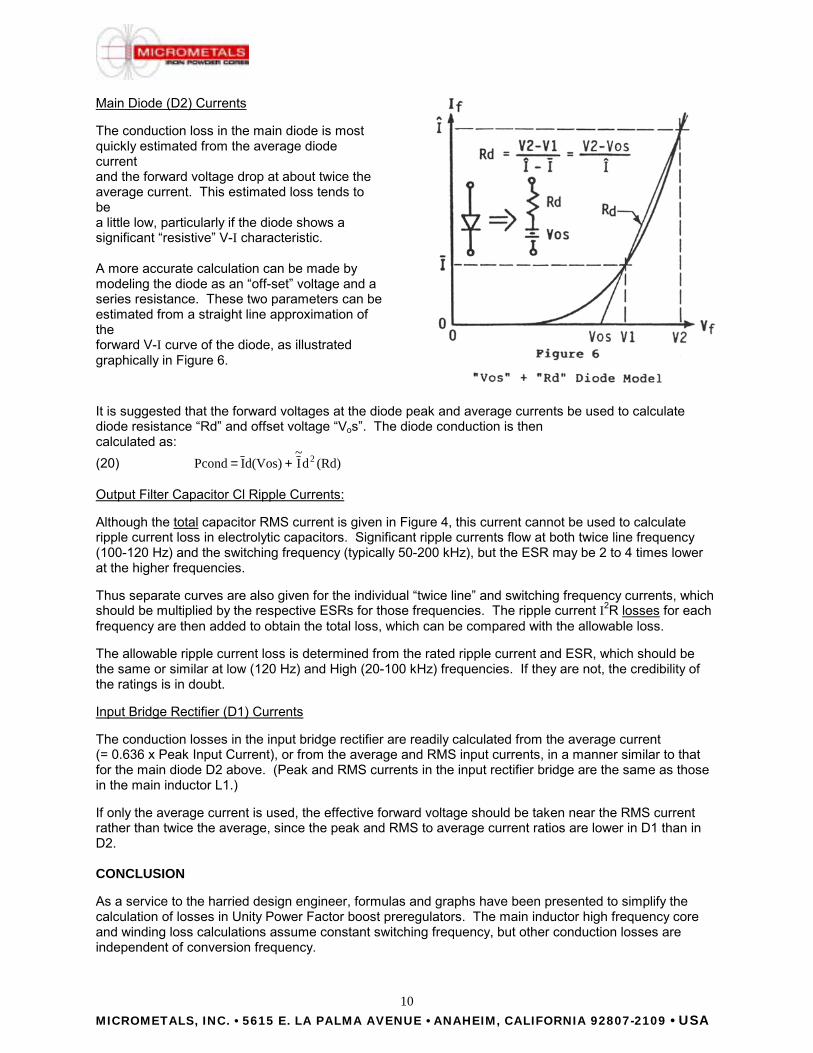
Main Diode (D2) Currents The conduction loss in the main diode is most quickly estimated from the average diode current and the forward voltage drop at about twice the average current. This estimated loss tends to be a little low, particularly if the diode shows a significant �resistive� V-I characteristic. A more accurate calculation can be made by modeling the diode as an �off-set� voltage and a series resistance. These two parameters can be estimated from a straight line approximation of the forward V-I curve of the diode, as illustrated graphically in Figure 6.
It is suggested that the forward voltages at the diode peak and average currents be used to calculate diode resistance �Rd� and offset voltage �Vos�. The diode conduction is then calculated as: (20) (Rd)dI
~ d(Vos)I Pcond 2+=
Output Filter Capacitor Cl Ripple Currents: Although the total capacitor RMS current is given in Figure 4, this current cannot be used to calculate ripple current loss in electrolytic capacitors. Significant ripple currents flow at both twice line frequency (100-120 Hz) and the switching frequency (typically 50-200 kHz), but the ESR may be 2 to 4 times lower at the higher frequencies. Thus separate curves are also given for the individual �twice line� and switching frequency currents, which should be multiplied by the respective ESRs for those frequencies. The ripple current I2R losses for each frequency are then added to obtain the total loss, which can be compared with the allowable loss. The allowable ripple current loss is determined from the rated ripple current and ESR, which should be the same or similar at low (120 Hz) and High (20-100 kHz) frequencies. If they are not, the credibility of the ratings is in doubt. Input Bridge Rectifier (D1) Currents The conduction losses in the input bridge rectifier are readily calculated from the average current (= 0.636 x Peak Input Current), or from the average and RMS input currents, in a manner similar to that for the main diode D2 above. (Peak and RMS currents in the input rectifier bridge are the same as those in the main inductor L1.) If only the average current is used, the effective forward voltage should be taken near the RMS current rather than twice the average, since the peak and RMS to average current ratios are lower in D1 than in D2. CONCLUSION As a service to the harried design engineer, formulas and graphs have been presented to simplify the calculation of losses in Unity Power Factor boost preregulators. The main inductor high frequency core and winding loss calculations assume constant switching frequency, but other conduction losses are independent of conversion frequency.

MICROMETALS, INC. • 5615 E. LA PALMA AVENUE • ANAHEIM, CALIFORNIA 92807-2109 • USA
11
BIBLIOGRAPHY [1] B. Carsten; �CONVERTER COMPONENT LOAD FACTORS; A PERFORMANCE LIMITATION OF VARIOUS TOPOLOGIES�, Proceedings of PCI�88, Munich, West Germany [2] P. L. Dowell: �EFFECTS OF EDDY CURRENTS IN TRANSFORMER WINDINGS�, Proceedings of the IEE, Vol. 113, No. 8, August 1966, pp. 1387-1394 (The paper on which much subsequent work is based.) [3] B. Carsten; �HIGH FREQUENCY CONDUCTOR LOSSES IN SWITCHMODE MAGNETICS� Proceedings of HFPC �86, Virginia Beach, VA Proceedings of PCI �86, Munich, West Germany PCIM Magazine, November 1986 (revised version) [4] J. P. Vandelac & P. Ziogas; �A NOVEL APPROACH FOR MINIMIZING HIGH FREQUENCY TRANSFORMER COPPER LOSSES�; IEE Power Electronics Specialists Conference Record, 87CH2459-6, 1987, pp. 355-367 (A recommended �general approach� paper.) [5] A. M. Urling et al; �CHARACTERIZING HIGH-FREQUENCY EFFECTS IN TRANSFORMER WINDINGS � A GUIDE TO SEVERAL SIGNIFICANT ARTICLES�; Proceedings of IEEE APEC �89 Conference, March 13-17, 1989, Baltimore, MA (A good overview Paper, with additional references.) [6] R. Severns: �A SIMPLE, GENERAL METHOD FOR CALCULATING HF WINDING LOSSES FOR ARBITRARY CURRENT WAVEFORMS�; Proceedings of HFPC �91, June 9-14 1991, Toronto, ON, Canada. (On the use of a computer spread sheet to calculate losses.)
MICROMETALS, INC. • 5615 E. LA PALMA AVENUE • ANAHEIM, CALIFORNIA 92807-2109 • USA
12