Embed Size (px)
Citation preview

SILICON THINKING INDUSTRY SOLUTION EXPERIENCETurn Technical Complexity into Market Profi tability
Advancements in integrated circuit (IC) density and competition for market leadership drive demand for more complex devices from semiconductor manufacturers. To compete successfully, manufacturers must use teams of diverse design specialists and complex project workfl ows to maximize device differentiation and team productivity. As a result, IC projects carry increasing business risk.
Dassault Systèmes Silicon Thinking Industry Solution Experience provides a portfolio of IC design and engineering performance enhancements that help mitigate project risk, shorten time-to-market, and increase product quality and yield. Silicon Thinking provides these benefi ts through:
• Effi cient intellectual property (IP) management and reuse • Graphical analytics to manage design closure• Instant access to the latest design data for all design teams• End-to-end traceability, from requirements to verifi cation and validation • Packaging reliability simulation and testing• Enhanced product variation and defect management
With this solution portfolio, semiconductor manufacturers can more quickly and easily untangle the simultaneous challenges they face from the demands of increasing chip complexity, lower-ing power consumption, and achieving faster time-to-production and higher yields.Semiconductor
Manufacturing Confi guration
Semiconductor Verifi vation & Validation
Semiconductor Collaborative Design
Semiconductor IP Management
Issue, Defect & Change Management
Semiconductor Packaging Simulation
Semiconductor Manufacturing Process Improvement
Requirement, Traceability & Test
Project & Portfolio Management

SEMICONDUCTOR COLLABORATIVE DESIGN PROCESS Enable collaborative design for complex semiconductor projects
Dassault Systèmes Silicon Thinking Semiconductor Collaborative Design process integrates deep design analytics from ENOVIA® Pinpoint® and design data management from ENOVIA Synchronicity® DesignSync® to enhance team productivity for IC design. This process experience is used today by over 120 IC development organizations around the world to boost design team productivity.
ENOVIA Synchronicity DesignSync
ENOVIA Synchronicity DesignSync helps centralize IC design data management for large, distributed projects. Design data is captured directly from electronic design automation (EDA) tools into a hierarchical data structure, which then provides coordi-nated access for distributed design teams. This hierarchical structure directly supports an IP-block assembly approach for rapidly designing customer-specific ICs. It helps simplify and speed integration of design sub-elements into the overall IC design, facilitating design reuse.
ENOVIA Pinpoint
ENOVIA Pinpoint provides managers with dashboards and graphical analytics to assess and accelerate design closure. ENOVIA Pinpoint enables analysis of diverse design, simulation, and testing data with historical timelines to help you see where projects might be diverging from planned milestones. Project managers and designers have a shared view from which to make joint project management decisions.
To help ensure that complex integrated designs succeed, the right foundation for collaborative design and information systems is essential. Dassault Systèmes Silicon Thinking Semiconductor Collaborative Design process:
• Scales across large, distributed teams • Supports IP reuse and variant optimization • Works with multiple application platforms and keeps designers “designing” • Maximizes information access• Accelerates project decision making through automated, advanced analytics, and dashboards
13OF THE TOP
15semicondictor companies
around the world are using Dassault Systèmes
Silicon Thinking Collaborative Design to
boost design productivity

ENOVIA PINPOINTAdvanced analytics and dashboards
for design closure
ENOVIA Pinpoint facilitates on-time delivery by providing communication, tracking, and predictability for your semiconductor design teams. The goal is to make designs feel tangible, at a scale that is manageable, and with views into design data for rapid issue resolution and design closure.
CHALLENGES OF THE IC DESIGN PROCESSEvery day, IC design tape-out schedules are slipping. Managers know they need to assess and resolve issues faster, but closure always seems a few days away with limited visibility into remaining problems.
Underlying these issues are multiple challenges:
1) Design closure becomes geometrically more complicated as IP blocks are added to an IC floor plan.
2) Design closure requires balancing conflicting requirements for functional timing, low power consumption, minimum floor plan, maximum manu-facturability, high performance (speed), and eliminating hotspots.
3) Different tools are used to assure compliance for different specifications. Each generates results in different data formats, few (or none) of which can be comparatively analyzed in one analytic graph or chart without hand editing a spreadsheet.
4) Design closure often requires multiple design/test/evaluate iterations as different solutions are proposed for various engineering problems, which can negatively impact time-to-design-completion.
What causes these issues and pain points?
1) The primary causes of delay and low product quality are the counteract-ing combination of IC project complexity, low efficiency design, testing, and limited results analysis tools.
2) Ineffective communication between engineers and teams impedes time-ly and high-quality design completion. Communication can be inhibited by geographic location, time zones, spoken language, culture, skill set, and process knowledge.
3) Limited budget for design tool licenses needed for collaborative analysis.
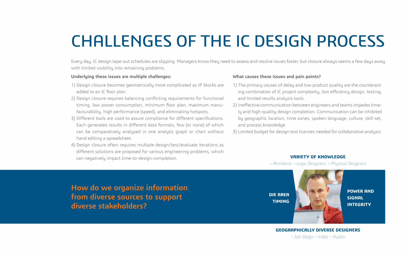
VARIETY OF KNOWLEDGE• Architects • Logic Designers • Physical Designers
GEOGRAPHICALLY DIVERSE DESIGNERS• San Diego • India • Austin
DIE AREATIMING
POWER AND SIGNAL INTEGRITY
How do we organize information from diverse sources to support diverse stakeholders?

DISTILL DATA AND ANALYTICS INTO DESIGN INFORMATIONFinding problems before they become critical
From the start of physical design, ENOVIA Pinpoint enables engineers and managers responsible for design closure to see and analyze the entire progress of the IC design and how metrics are trend-ing toward their goals. ENOVIA Pinpoint takes the vast arrays of multi-dimensional data, analyzes them, and collects them into a simple visual dashboard with historical timelines to help you see where things might be trending off track. This trending view provides context and improves com-munication between engineers and managers.
With ENOVIA Pinpoint, you gain critical troubleshooting information to get your design closed and taped-out sooner. Data can include timing, power consumption, heat, and IR drop. All data resides on a central project server that you can access through links and a browser. Your design teams can communicate and collaborate better because consolidated views show results from different tasks and disciplines, improving shared understanding across design and verifi cation.
ENOVIA PinPoint facilitates IC design team collaboration
and decision making through data visualization from
multiple IC design tools

INTEGRATED ANALYSIS FOR FAST ROOT CAUSE INVESTIGATIONQuickly assess key design interactions
• Interactive plots – Pop-up and drill-down interactivity facilitates rapid root cause answers
• Confi gurable views – Choose and present the data that is most critical to your team’s success, quickly identify and investigate outliers
• Zoom and Pan – Traverse and zoom fl oor plan graphics to see high level issue assess-ment, then zoom in for troubleshooting, from event to cell level
Zoom and Pan
Interactive plots
Confi gurable views

ASSESS MULTIPLE CHIP DESIGN FACTORS COLLECTIVELYReview Timing, Path, Floor Plan design elements
• Identify fl oor plan improvements – Overlay fl oor plans with critical paths, IR drop, or hotspots
• Summary path data – Identify architectural timing bottlenecks
• Timing reports – Identify specifi c path delays to focus redesign work, then click through to see the timing path overlaid on the design fl oor plan
Timing reports
Identify fl oor plan improvements
Summary path data

PROVEN RESULTSENOVIA Pinpoint is built on a stable fifth generation platform with over 75 man-years of development and has been used on IC production designs for many years. Its ability to process and display semiconductor physical design data enables rapid collaborative deci-sion making for semiconductor projects. The tool doesn’t just track metrics—it provides a medium for collaborative project management, with everyone on the same page about project status.
Besides the benefits from better decision making, ENOVIA Pinpoint helps focus attention on priority design issues, reducing distractions and automating status report generation with objective data, not subjective updates. In other words, ENOVIA Pinpoint helps im-prove productivity and the time your engineers spend on their work.
With ENOVIA Business Impact of Collaborative Design Using DesignSync Average % ImprovementProductivity Improvements 43%Design Engineering Time Saved 46%Multi-site Design Projects 74%IP Re-use 44%Product and Manufacturing Schedules 20%Manufacturing Cost Savings 25%Design/Product Quality 32%
MISSED DEADLINES...due to resources not being synchronized or having to correct avoidable problems
EXCESSIVE DESIGN RE-SPINS AND WAIVERS...due to wrong data being handed off for tape-out or late changes being introduced without review
HIGH COST OF DESIGN...due to inability to leverage resources and IP across your design chain
REDUCING
WHAT OUR CUSTOMERS ARE SAYINGThe beauty of ENOVIA Pinpoint is that with a single click, you see a graphical representation of the path, with the green-dot to red-dot path indicating where you need to go [to address the glitch]. It’s as easy to use as Google Maps, as the tool zooms down to a single instance, which allows you to diagnose the particular problem. Then you can zoom all the way back out and map all of the failing paths and compare them to your layout.
— Dwight Galbi, Principle/Manager, Qualcomm
Learn how ENOVIA Pinpoint and Dassault Systèmes Silicon Thinking Industry Solution Experience can fit into your IC design process.
Contact Sales for a custom evaluation and more information about the following:
• Project & Portfolio Management • Requirement, Traceability & Test • Issue, Defect & Change Management
• Semiconductor Collaboration Design • Semiconductor Package Simulation
Our 3DEXPERIENCE platform powers our brand applications, serving 12 industries, and provides a rich portfolio of industry solution experiences.Dassault Systèmes, the 3DEXPERIENCE® Company, provides business and people with virtual universes to imagine sustainable innovations. Its world-leading solutions transform the way products are designed, produced, and supported. Dassault Systèmes’ collaborative solutions foster social innovation, expanding possibilities for the virtual world to improve the real world. The group brings value to over 170,000 customers of all sizes in all industries in more than 140 countries. For more information, visit www.3ds.com.
Europe/Middle East/AfricaDassault Systèmes10, rue Marcel DassaultCS 4050178946 Vélizy-Villacoublay CedexFrance
AmericasDassault Systèmes175 Wyman StreetWaltham, Massachusetts02451-1223USA
Asia-Pacifi cDassault Systèmes K.K.ThinkPark Tower2-1-1 Osaki, Shinagawa-ku,Tokyo 141-6020Japan