Embed Size (px)
Citation preview
www.luxtera.comLuxtera Proprietary
Silicon Photonics Transceivers for Hyper‐Scale Datacenters: Deployment and Roadmap
Peter De DobbelaereLuxtera Inc.
09/19/2016
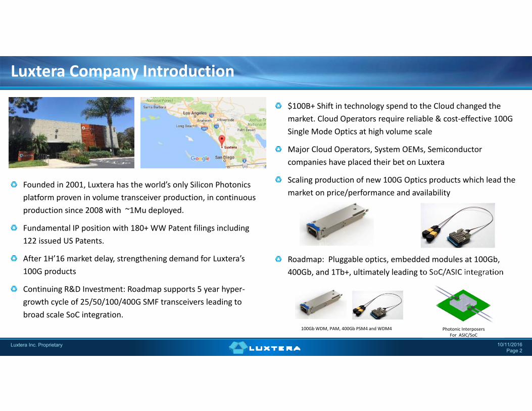
Founded in 2001, Luxtera has the world’s only Silicon Photonics platform proven in volume transceiver production, in continuous production since 2008 with ~1Mu deployed.
Fundamental IP position with 180+ WW Patent filings including 122 issued US Patents.
After 1H’16 market delay, strengthening demand for Luxtera’s100G products
Continuing R&D Investment: Roadmap supports 5 year hyper‐growth cycle of 25/50/100/400G SMF transceivers leading to broad scale SoC integration.
Luxtera Company Introduction
10/11/2016Page 2
$100B+ Shift in technology spend to the Cloud changed the market. Cloud Operators require reliable & cost‐effective 100G Single Mode Optics at high volume scale
Major Cloud Operators, System OEMs, Semiconductor companies have placed their bet on Luxtera
Scaling production of new 100G Optics products which lead the market on price/performance and availability
Roadmap: Pluggable optics, embedded modules at 100Gb, 400Gb, and 1Tb+, ultimately leading to SoC/ASIC integration
Luxtera Inc. Proprietary
Photonic InterposersFor ASIC/SoC
100Gb WDM, PAM, 400Gb PSM4 and WDM4
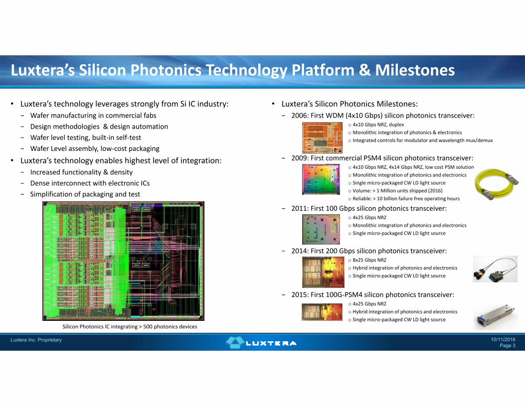
• Luxtera’s technology leverages strongly from Si IC industry:− Wafer manufacturing in commercial fabs− Design methodologies & design automation− Wafer level testing, built‐in self‐test− Wafer Level assembly, low‐cost packaging
• Luxtera’s technology enables highest level of integration:− Increased functionality & density− Dense interconnect with electronic ICs− Simplification of packaging and test
Luxtera’s Silicon Photonics Technology Platform & Milestones
10/11/2016Page 3
• Luxtera’s Silicon Photonics Milestones:− 2006: First WDM (4x10 Gbps) silicon photonics transceiver:
o 4x10 Gbps NRZ, duplexo Monolithic integration of photonics & electronicso Integrated controls for modulator and wavelength mux/demux
− 2009: First commercial PSM4 silicon photonics transceiver:o 4x10 Gbps NRZ, 4x14 Gbps NRZ, low cost PSM solutiono Monolithic integration of photonics and electronicso Single micro‐packaged CW LD light sourceo Volume: > 1 Million units shipped (2016)o Reliable: > 10 billion failure free operating hours
− 2011: First 100 Gbps silicon photonics transceiver:o 4x25 Gbps NRZo Monolithic integration of photonics and electronicso Single micro‐packaged CW LD light source
− 2014: First 200 Gbps silicon photonics transceiver: o 8x25 Gbps NRZo Hybrid integration of photonics and electronicso Single micro‐packaged CW LD light source
− 2015: First 100G‐PSM4 silicon photonics transceiver:o 4x25 Gbps NRZo Hybrid integration of photonics and electronicso Single micro‐packaged CW LD light source
Silicon Photonics IC integrating > 500 photonics devices
Luxtera Inc. Proprietary
Integration Photonics & Electronics
10/11/2016Page 4
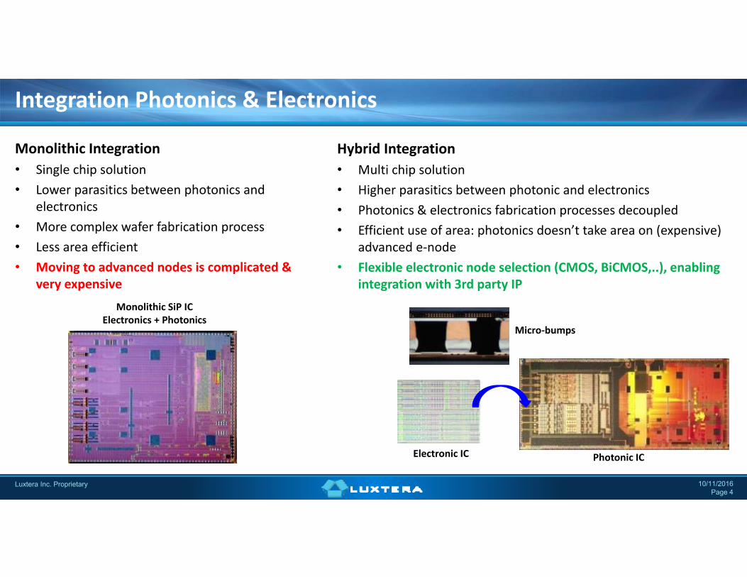
Monolithic Integration• Single chip solution• Lower parasitics between photonics and
electronics• More complex wafer fabrication process • Less area efficient• Moving to advanced nodes is complicated &
very expensive
Hybrid Integration• Multi chip solution• Higher parasitics between photonic and electronics• Photonics & electronics fabrication processes decoupled• Efficient use of area: photonics doesn’t take area on (expensive)
advanced e‐node• Flexible electronic node selection (CMOS, BiCMOS,..), enabling
integration with 3rd party IPMonolithic SiP IC
Electronics + Photonics
Photonic IC
Micro‐bumps
Electronic IC
Luxtera Inc. Proprietary
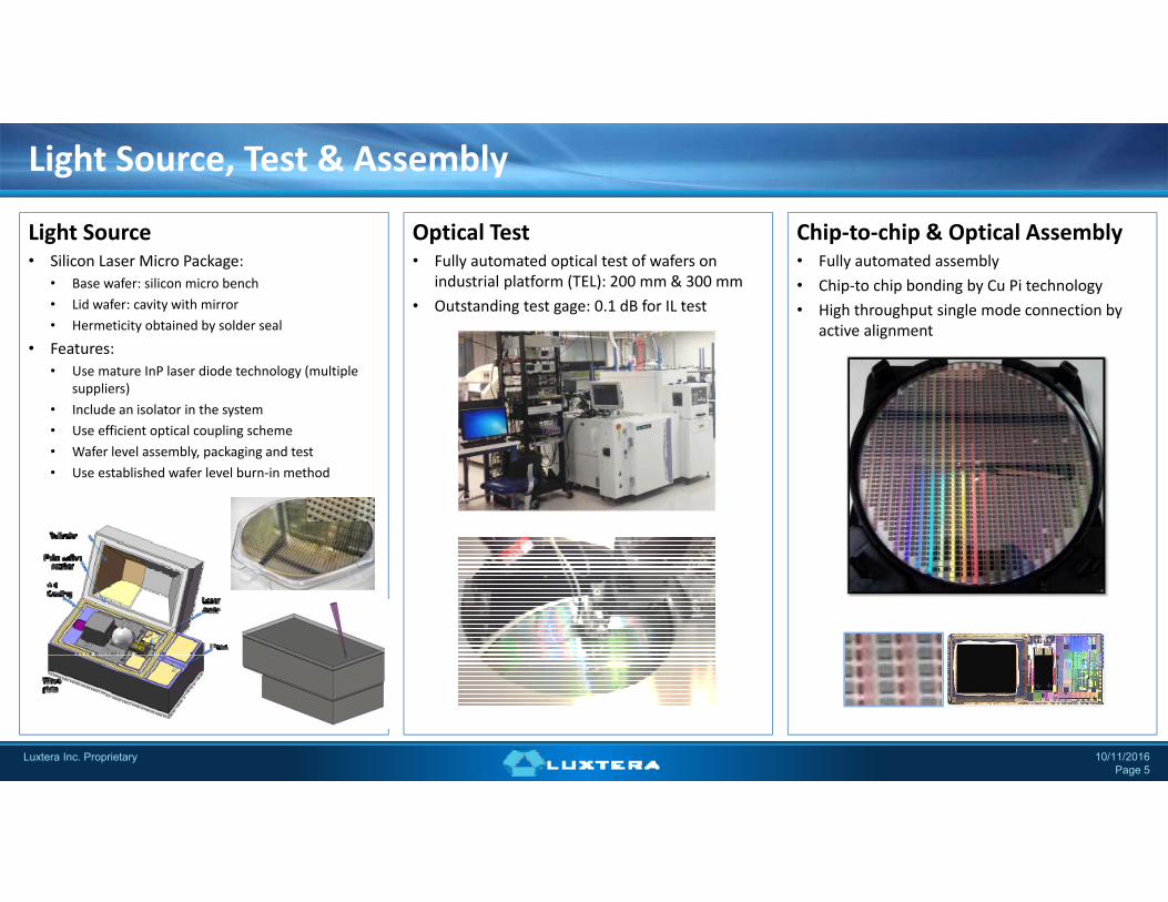
Light Source• Silicon Laser Micro Package:
• Base wafer: silicon micro bench• Lid wafer: cavity with mirror• Hermeticity obtained by solder seal
• Features: • Use mature InP laser diode technology (multiple
suppliers)• Include an isolator in the system• Use efficient optical coupling scheme• Wafer level assembly, packaging and test• Use established wafer level burn‐in method
Light Source, Test & Assembly
10/11/2016Page 5
Optical Test• Fully automated optical test of wafers on
industrial platform (TEL): 200 mm & 300 mm• Outstanding test gage: 0.1 dB for IL test
Chip‐to‐chip & Optical Assembly• Fully automated assembly • Chip‐to chip bonding by Cu Pi technology• High throughput single mode connection by
active alignment
Luxtera Inc. Proprietary
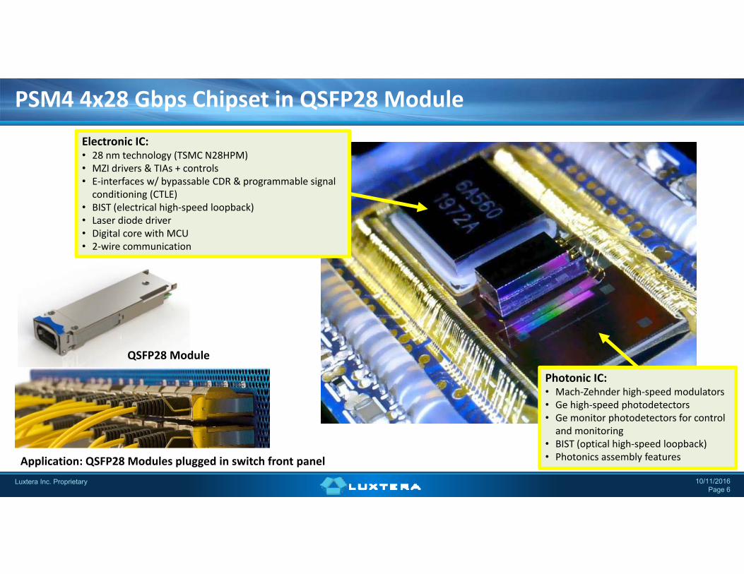
PSM4 4x28 Gbps Chipset in QSFP28 Module
10/11/2016Page 6
Photonic IC:• Mach‐Zehnder high‐speed modulators• Ge high‐speed photodetectors• Ge monitor photodetectors for control and monitoring
• BIST (optical high‐speed loopback)• Photonics assembly features
Electronic IC:• 28 nm technology (TSMC N28HPM)• MZI drivers & TIAs + controls• E‐interfaces w/ bypassable CDR & programmable signal conditioning (CTLE)
• BIST (electrical high‐speed loopback)• Laser diode driver• Digital core with MCU• 2‐wire communication
QSFP28 Module
Application: QSFP28 Modules plugged in switch front panelLuxtera Inc. Proprietary
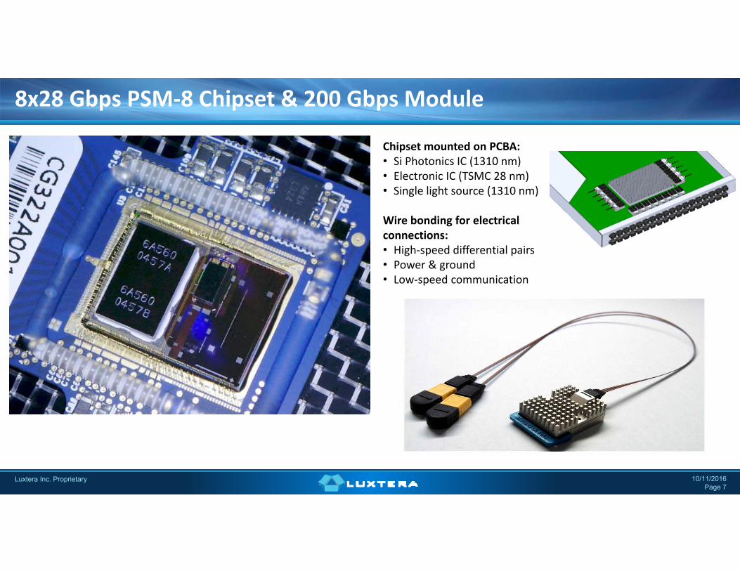
8x28 Gbps PSM‐8 Chipset & 200 Gbps Module
Luxtera Inc. Proprietary 10/11/2016Page 7
Chipset mounted on PCBA:• Si Photonics IC (1310 nm)• Electronic IC (TSMC 28 nm)• Single light source (1310 nm)
Wire bonding for electrical connections:• High‐speed differential pairs• Power & ground• Low‐speed communication
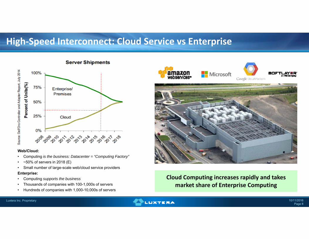
High‐Speed Interconnect: Cloud Service vs Enterprise
Luxtera Inc. Proprietary 10/11/2016Page 8
Cloud Computing increases rapidly and takes market share of Enterprise Computing
Cloud Computing increases rapidly and takes market share of Enterprise Computing
Web/Cloud:• Computing is the business: Datacenter = “Computing Factory”• ~50% of servers in 2018 (E)• Small number of large-scale web/cloud service providersEnterprise:• Computing supports the business• Thousands of companies with 100-1,000s of servers• Hundreds of companies with 1,000-10,000s of servers
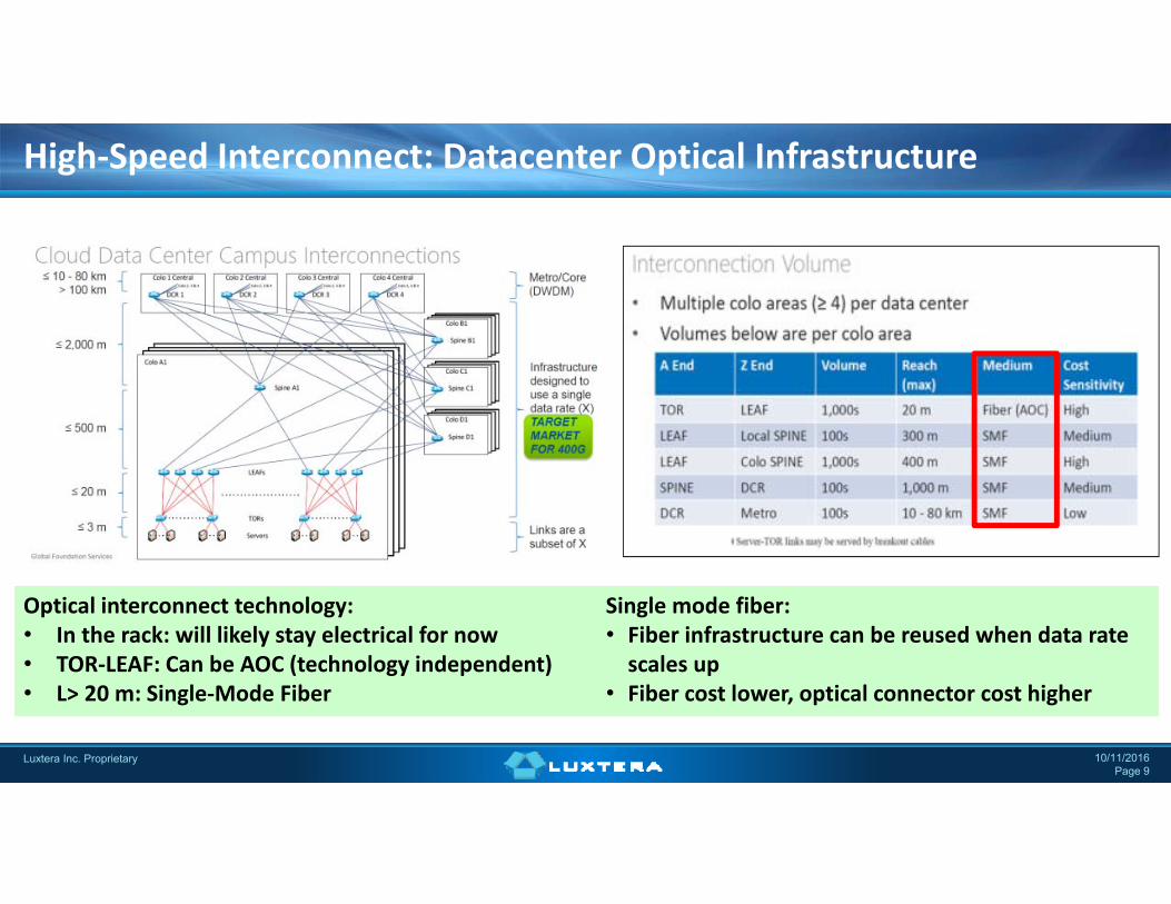
Optical interconnect technology: • In the rack: will likely stay electrical for now• TOR‐LEAF: Can be AOC (technology independent)• L> 20 m: Single‐Mode Fiber
High‐Speed Interconnect: Datacenter Optical Infrastructure
Luxtera Inc. Proprietary 10/11/2016Page 9
Single mode fiber:• Fiber infrastructure can be reused when data rate scales up
• Fiber cost lower, optical connector cost higher
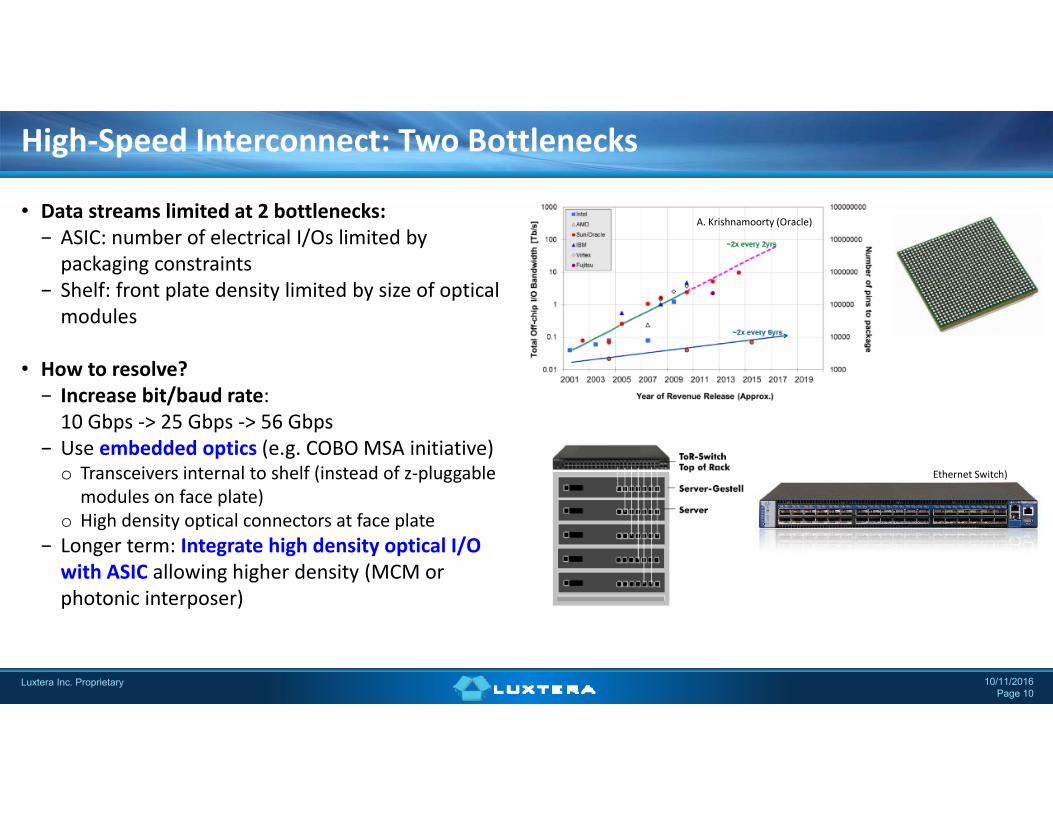
• Data streams limited at 2 bottlenecks:− ASIC: number of electrical I/Os limited by packaging constraints
− Shelf: front plate density limited by size of optical modules
• How to resolve?− Increase bit/baud rate:10 Gbps ‐> 25 Gbps ‐> 56 Gbps
− Use embedded optics (e.g. COBO MSA initiative)o Transceivers internal to shelf (instead of z‐pluggable
modules on face plate)o High density optical connectors at face plate
− Longer term: Integrate high density optical I/O with ASIC allowing higher density (MCM or photonic interposer)
High‐Speed Interconnect: Two Bottlenecks
Luxtera Inc. Proprietary 10/11/2016Page 10
A. Krishnamoorty (Oracle)
Ethernet Switch)
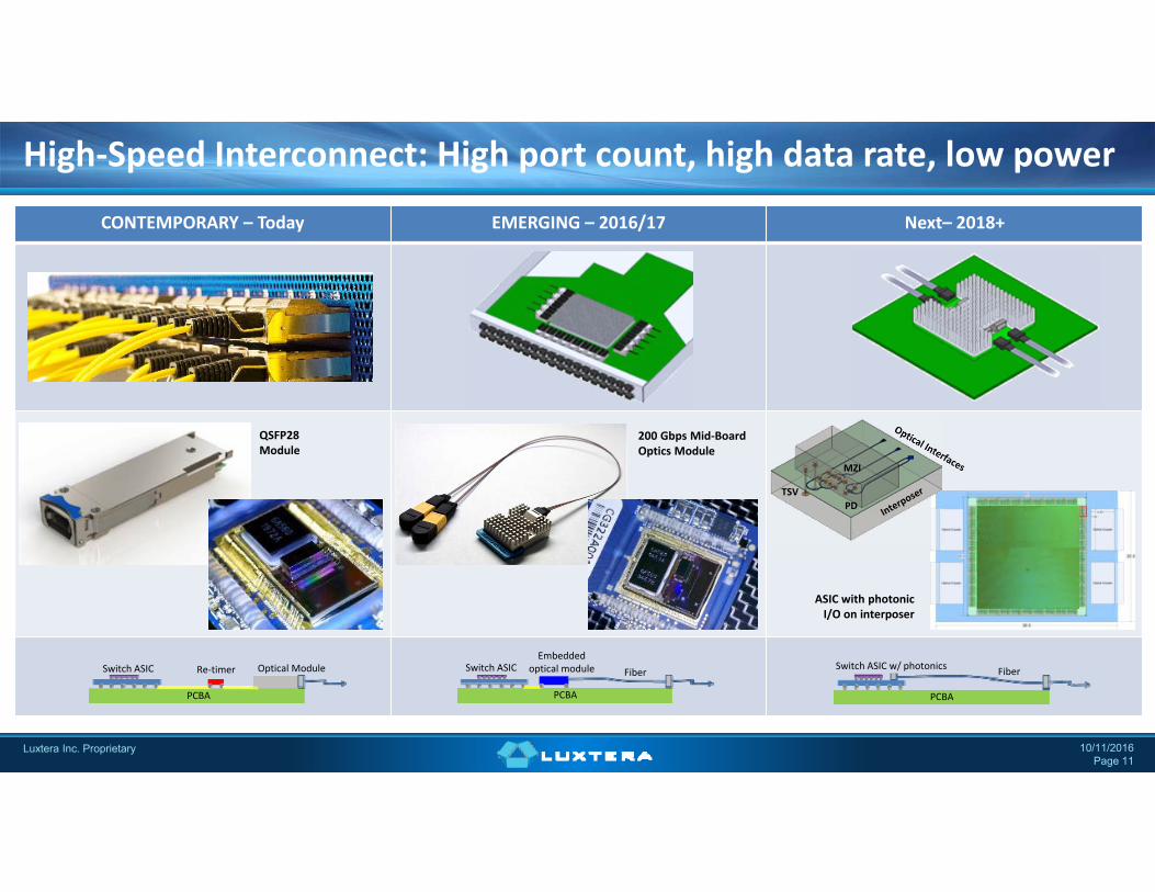
High‐Speed Interconnect: High port count, high data rate, low power
Luxtera Inc. Proprietary 10/11/2016Page 11
CONTEMPORARY – Today EMERGING – 2016/17 Next– 2018+
Embedded optical module FiberSwitch ASIC
PCBA
FiberSwitch ASIC w/ photonics
PCBA
Switch ASIC Re‐timer Optical Module
PCBA
ASIC with photonic I/O on interposer
QSFP28 Module
200 Gbps Mid‐Board Optics Module
TSV
MZI
PD
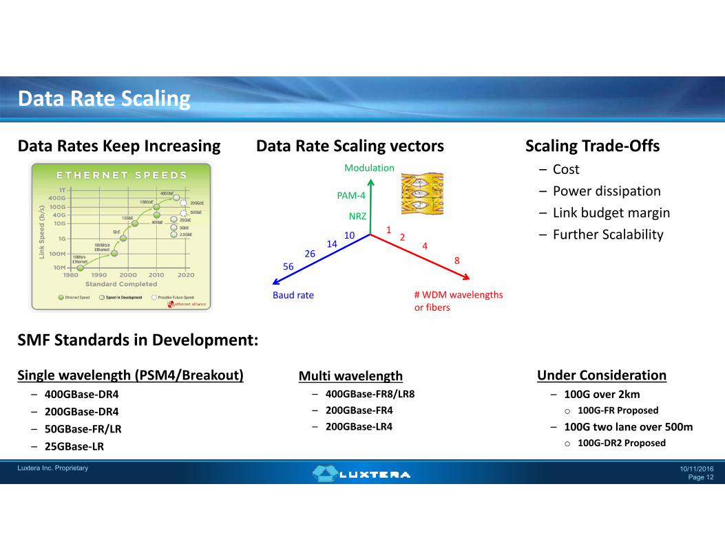
Data Rates Keep Increasing
Data Rate Scaling
10/11/2016Page 12
Luxtera Inc. Proprietary
Data Rate Scaling vectors Scaling Trade‐Offs– Cost– Power dissipation– Link budget margin– Further Scalability10
2614
56
12
48
NRZ
PAM‐4
Modulation
# WDM wavelengthsor fibers
Baud rate
Single wavelength (PSM4/Breakout)– 400GBase‐DR4– 200GBase‐DR4– 50GBase‐FR/LR– 25GBase‐LR
Multi wavelength– 400GBase‐FR8/LR8– 200GBase‐FR4– 200GBase‐LR4
Under Consideration– 100G over 2km
o 100G‐FR Proposed
– 100G two lane over 500mo 100G‐DR2 Proposed
SMF Standards in Development:
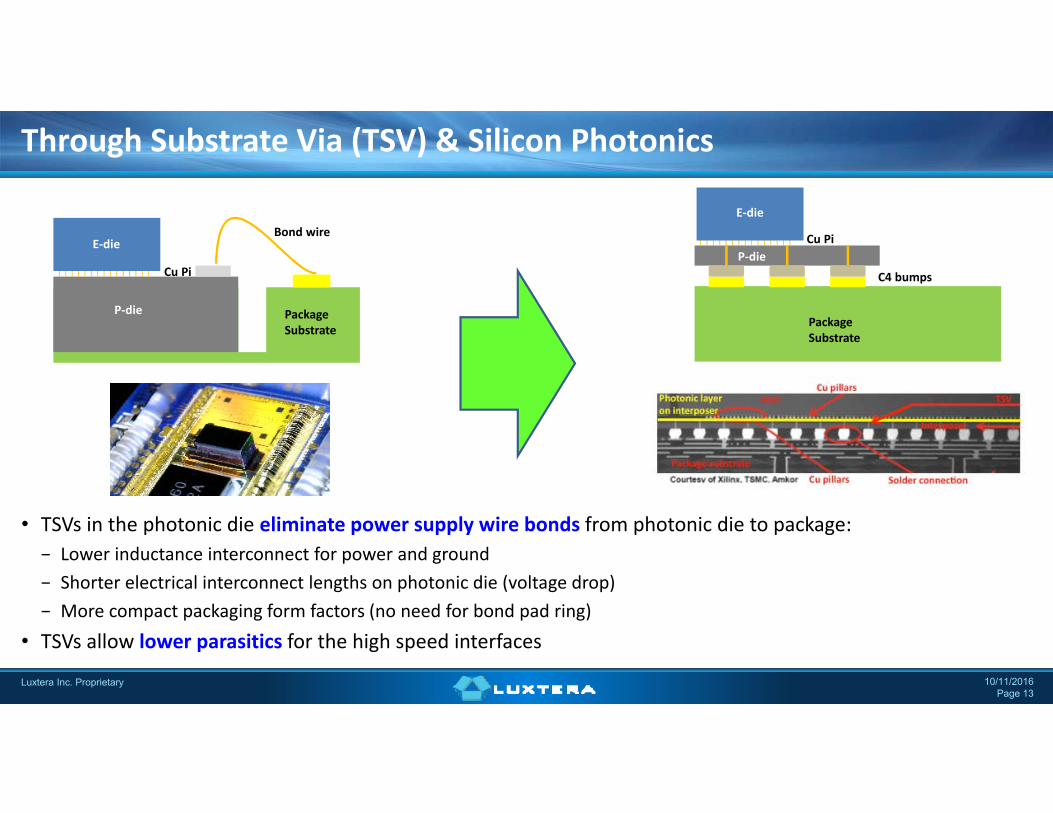
• TSVs in the photonic die eliminate power supply wire bonds from photonic die to package:− Lower inductance interconnect for power and ground− Shorter electrical interconnect lengths on photonic die (voltage drop)− More compact packaging form factors (no need for bond pad ring)
• TSVs allow lower parasitics for the high speed interfaces
Through Substrate Via (TSV) & Silicon Photonics
Luxtera Inc. Proprietary 10/11/2016Page 13
P‐die Package Substrate
E‐dieBond wire
Cu PiP‐die
Package Substrate
C4 bumps
E‐die
Cu Pi
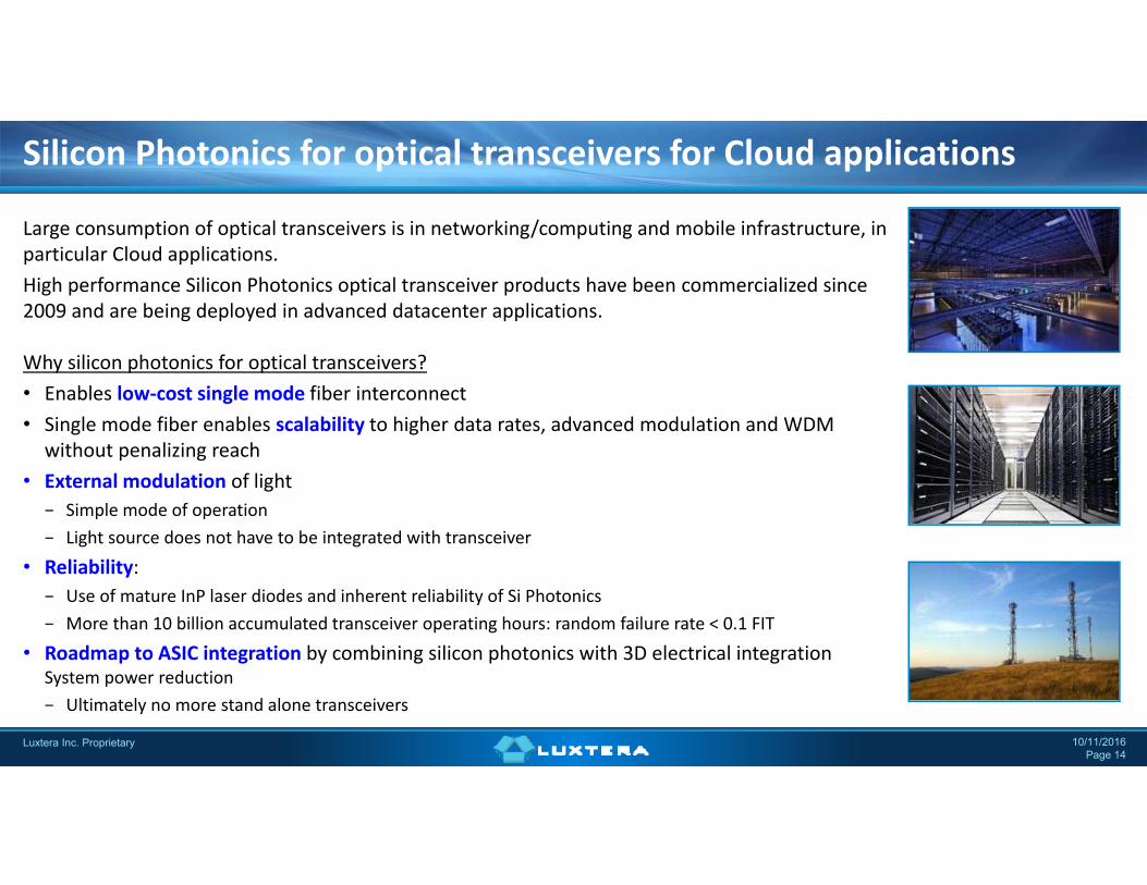
Large consumption of optical transceivers is in networking/computing and mobile infrastructure, in particular Cloud applications.High performance Silicon Photonics optical transceiver products have been commercialized since 2009 and are being deployed in advanced datacenter applications.
Why silicon photonics for optical transceivers?• Enables low‐cost single mode fiber interconnect • Single mode fiber enables scalability to higher data rates, advanced modulation and WDM
without penalizing reach• External modulation of light
− Simple mode of operation− Light source does not have to be integrated with transceiver
• Reliability:− Use of mature InP laser diodes and inherent reliability of Si Photonics− More than 10 billion accumulated transceiver operating hours: random failure rate < 0.1 FIT
• Roadmap to ASIC integration by combining silicon photonics with 3D electrical integration System power reduction− Ultimately no more stand alone transceivers
Silicon Photonics for optical transceivers for Cloud applications
Luxtera Inc. Proprietary 10/11/2016Page 14

www.luxtera.comLuxtera Proprietary
Acknowledgement:This presentation contains work of the entire Luxtera team and its technology partners, their
contributions are greatly acknowledged.
Thank you for your interest.