Embed Size (px)
Citation preview
POST-FABRICATION TRIMMING OF
SILICON-PHOTONIC DEVICES USING A
PHOTO-SENSITIVE UPPER CLADDING
Ran Califa
Faculty of Engineering,
Ph.D Thesis
Submitted to the Senate of Bar-Ilan University
Ramat-Gan, Israel October 2015

This work was carried out under the
supervision of Prof. Avi Zadok from the
Faculty of Engineering at Bar-Ilan University

Acknowledgements
Fulfillment of this work would not have been possible without the help and
contributions of many individuals, and now it is my pleasure to thank all of them for
their support, encouragement and blessing. First and foremost, I would like to express
my gratitude to my advisor, Prof. Avi Zadok. His encouragement and positive attitude
towards student ideas allowed me the academic freedom to pursue new and interesting
directions. His deep understanding and high involvement in research details gave me
the right support through the ups and downs of my research. And finally, his hard
working spirit, devotion to research and to his group members has inspired all of us.
Special thanks are given to Dvir Munk, who accompanied me throughout the
second half of my research. I would like to thank him for his major contribution in all
aspects, and mainly in simulations and in endless hours in the lab. I am also very
grateful to Hadar Genish, a good friend and colleague, for his help and support. His
creativity, high spirit and willingness to help anytime in any topic just amaze me
every time: free space setups, UV bonding and packaging, mechanical stages, and
many more.
I would also like to mention and thank Dr. Yuri Kaganovskii for all his help
related to chalcogenide glasses, from the evaporation of samples through to patiently
sharing his wide knowledge in material science with me and introducing me to the
mass-transfer mechanism, and to Prof. Michael Rosenbluh from the Physics
Department for his supportive ideas and for generously opening his lab for us.
I wish to thank all Avi‟s group members, past and present, for helping with
good advices and for creating a fun working environment: Dr. Arkady Rudnitsky, Dr.

Daniel Grodensky, Daniel Kravitz, David Elooz, Eyal Preter, Yoni Stern, Kun Zhong,
Ofir Klinger, Raphi Cohen, Shahar Levi, Tali Ilovitsh, Assaf Amram, Nadav Arbel,
Yossef London, Assaf Ben Amram, and Yair Antman.
Special thanks go to our former group member Idan Bakish, who accompanied
me during the first half of my research and helped me with his enthusiastic spirit to
develop the in-house Si-photonic process and shared useful tips in the art of drawing.
I would like to thank The Bar-Ilan Institute of Nanotechnology and Advanced
Materials (BINA) for the use of the clean room facilities In this context I want to
mention the contributions of Dr. Yossi Abulafia in sharing with me his wide
knowledge in Nano-fabrication, and of Dr. Yafit Fleger in her help with the focused
ion beam processing.
To the Faculty of Engineering at Bar-Ilan University, and especially to the
Head of Administration Mrs. Dina Yeminy who always finds time to give personal
attention, I would like to express my gratitude.
I acknowledge and appreciate the financial support of the University President
Scholarship throughout my Ph.D. studies, and the support and funding by the 'Tera
Santa' Consortium of the Chief Scientist Office of the Israeli Ministry of Economy. I
enjoyed and benefited from collaborations with colleagues within the consortium,
especially with Dr. Yosef Ben-Ezra (Cello-Wireless) and Menachem Vofsy (Tower-
Jazz).
Last but not least, I would like to express my gratitude to my parents and
family, for their endless love - and much more.
With a little help from my friends…
Oct. 2015
Table of Contents
ABSTRACT .............................................................................................................................. I
INTRODUCTION ................................................................................................................. 1
1.1 INTEGRATED PHOTONICS ON SILICON: WHY AND WHERE .................................................. 1
1.2 PASSIVE OPTICAL DEVICES AND FILTERS IN SILICON ......................................................... 3
1.3 SI-PHOTONICS FABRICATION TOLERANCES ..................................................................... 20
1.4 OVERVIEW OF FOR POST-FABRICATION DEVICE TRIMMING ............................................. 21
1.5 RESEARCH OBJECTIVES .................................................................................................. 26
THE CHALCOGENIDE GLASS ON SILICON PHOTONIC PLATFORM ............... 28
2.1 WHAT ARE CHALCOGENIDE GLASSES? ............................................................................ 28
2.2 PHOTO-INDUCED EFFECTS IN CHALCOGENIDE GLASSES .................................................. 30
2.3 CHALCOGENIDE GLASS AS AN UPPER CLADDING OF SILICON-PHOTONIC DEVICES ........... 33
FABRICATION PROCEDURES ...................................................................................... 34
3.1 S I-PHOTONICS DEVICE FABR ICATION .................................................................... 34
3.2 FABRICATION OF CHALCOGENIDE GLASS UPPER CLADDING ............................. 38
3.3 PACKAGING ................................................................................................................ 41
SETUPS FOR THE TRIMMING AND CHARACTERIZATION OF DEVICES ....... 44
4.1 VERTICAL COUPLING CHARACTERIZATION SETUP ........................................................... 44
4.2 PASSIVE SI-PHOTONIC DEVICES CHARACTERIZATION ...................................................... 49
4.3 MASS-TRANSFER TRIMMING SETUP ................................................................................. 56
PHASE AND GROUP INDEX TRIMMING .................................................................... 59
5.1 MOTIVATION .................................................................................................................. 59
5.2 PHASE TRIMMING PRINCIPLES AND SIMULATIONS ........................................................... 60
5.3 GROUP INDEX TRIMMING THEORY AND SIMULATIONS ..................................................... 67
5.4 EXPERIMENTAL RESULTS ................................................................................................ 70
5.5 DISCUSSION AND SUMMARY ........................................................................................... 76

DIRECTIONAL COUPLER TRIMMING ....................................................................... 78
6.1 MOTIVATION .................................................................................................................. 78
6.2 THEORY AND SIMULATION .............................................................................................. 79
6.3 EXPERIMENTS RESULTS .................................................................................................. 82
6.4 DISCUSSION AND SUMMARY ........................................................................................... 90
TRIMMING OF CASCADED FILTERS ......................................................................... 92
7.1 MOTIVATION .................................................................................................................. 92
7.2 THEORETICAL BACKGROUND .......................................................................................... 92
7.3 EXPERIMENTAL RESULTS ................................................................................................ 96
7.4 DISCUSSION AND SUMMARY ......................................................................................... 104
OPTICAL ORTHOGONAL WAVELET DOMAIN MULTIPLEXING USING
PHOTONIC DEVICES ....................................................................................................... 106
8.1 MOTIVATION ................................................................................................................ 106
8.2 THEORETICAL BACKGROUND ........................................................................................ 108
8.3 REALIZATION IN THE OPTICAL DOMAIN......................................................................... 114
8.4 DISCUSSION AND SUMMARY ......................................................................................... 118
CONCLUSIONS AND PERSPECTIVE ......................................................................... 120
9.1 SUMMARY..................................................................................................................... 120
9.2 LOSS MECHANISMS IN THE CHALCOGENIDE-ON-SOI PLATFORM ................................... 122
9.3 TEMPERATURE SENSITIVITY .......................................................................................... 125
9.4 STABILITY AND DEGRADATION OVER TIME ................................................................... 126
BIBLIOGRAPHY ................................................................................................................ 128
HEBREW ABSTRACT………….…………………………………….……………………א
List of Figures
Figure 1. Applications of integrated photonic filters ........................................ 4
Figure 2. Slab waveguide illustration. .............................................................. 6
Figure 3. Three Si-photonics waveguides cross-sections.. ............................... 9
Figure 4. Directional coupler schematics. ....................................................... 10
Figure 5. Illustration of an integrated-photonic MZI ...................................... 13
Figure 6. Simulated power transfer function of a silicon-photonic MZI ........ 14
Figure 7. Schematic illustration of an integrated-photonic ring resonator ..... 15
Figure 8. Simulated transfer funtion of an intergrated-photonic ring. ............ 16
Figure 9. Luxtera 4x10 Gbit/s full tranciever on single chip, using Si-
photonics technology ....................................................................................... 19
Figure 10. Kotura 100 Gbit/s WDM transmitter and receiver modules, based
on Si-photonics technology.............................................................................. 19
Figure 11. . SEM image of an ultra-compact, sharp photonic filter containing
5 cascaded ring resonators, fabricated by IBM labs. ....................................... 20
Figure 12. Illustration of width and height inaccuracies in the fabrication of
silicon-photonic waveguides ............................................................................ 21
Figure 13. Active post fabrication trimming techniques ................................. 22
Figure 14. Trimming of micro-ring array using the irradiation of an upper
cladding layer of UV-sensitive polymer .......................................................... 23
Figure 15. Triming the effective index of silicon waveguides by introducing
stress to an upper silica cladding layer ............................................................ 24
Figure 16. Trimming the response of a silicon-photonic ring resonator through
illuminating an upper cladding layer of chalcogenide glass ............................ 25
Figure 17.Illustrations of photo-induced trimming of the basic properties of
ChG-on-SOI photonic filters............................................................................ 26
Figure 18. Amorphous chalcogenide glass film structure............................... 29
Figure 19. Illustration of the definition of a waveguide core through a photo-
darkening effect ............................................................................................... 32
Figure 20. Illustration of the photo-induced mass transfer effect ................... 32
Figure 21. Fabrication process flow. ............................................................... 34
Figure 22. Schematic cross-section of the SOI wafers used in this work ....... 35
Figure 23. Thermal evaporation chamber used in the deposition of
chalcogende glasses. ........................................................................................ 40
Figure 24. A Si-photonic MZI with a chalcogenide glass patch on top.......... 40
Figure 25. Design of a perspex fiber holder used in the bonding of input and
output fibers to devices under test. .................................................................. 41
Figure 26. Attaching fibers to a chip using a UV-curable adhesive ............... 42
Figure 27. Image of a packaged SOI device.. ................................................. 43
Figure 28. Illustration of the fiber-to-chip coupling problem. ........................ 44
Figure 29. Illustration of a vertical grating coupler ........................................ 45
Figure 30. Phase index matching condition for an input light beam that is
incident at an angle.. ........................................................................................ 46
Figure 31. Device characterization setup ........................................................ 47
Figure 32. Laboratory setup for device transfer function characterization ..... 48
Figure 33. Top-view SEM image of a Si ridge waveguide and a SEM image
of a FIB-processed cross section ...................................................................... 49
Figure 34. Atomic fornce microscope scanning profiles of a silicon-photonic
waveguide. ....................................................................................................... 50

Figure 35. Measured end-to-end losses of silicon-photonic ridge waveguides
of different lengths ........................................................................................... 50
Figure 36. Measured power transfer function of a silicon-photonic MZI with
optimized 50% directional couplers................................................................. 52
Figure 37. A FIB cross-section of a directional coupler within a silicon-
photonic MZI device. ....................................................................................... 53
Figure 38. Measured power transfer function of a ring resonator with 125 µm
circumference ................................................................................................... 54
Figure 39. Top-view SEM image of silicon-photonic ring resonator ............. 54
Figure 40. Numercial simulations of bending losses in an SOI ridge
waveguide, calculated using FIMMWAVE commercial software .................. 56
Figure 41. Measured absorption spectra of As2S3 and As10Se90 ................. 57
Figure 42. Schematic illustration of the mass-transfer-based trimming setup
and a photo of the setup.. ................................................................................. 58
Figure 43. Photo-induced index change in As2S3 vs. illumination intensity. 61
Figure 44. Change in the effective index of waveguides as a function of the
photo-darkening index change in an upper chalcogenide laye ........................ 63
Figure 45. Calculated changes to the effective index of a fully-etched
waveguide as a function of the thickness of a silica buffer layer... ................. 64
Figure 46. Waveguide effective index change vs. residual thickness of an
upper cladding layer ......................................................................................... 65
Figure 47. Calculated changes to the effective index of a fully-etched
waveguide as a function of the thickness of a silica buffer layer, following the
complete photo-removal of the upper cladding layer. ..................................... 67

Figure 48. Group delay index vs. the refractive index of an upper cladding
layer.................................................................................................................. 69
Figure 49. Group delay index vs. the residual thickness of an upper cladding
layer.................................................................................................................. 70
Figure 50. Top view optical microscope image of the a SOI MZI following
the photo-removal of an upper cladding layer from four patches. ................... 71
Figure 51. Measured power transfer functions of a SOI MZI following the
photo-removal of an upper cladding layer from four patches. ......................... 72
Figure 52. Top-view optical microscope inage of a SOI sample containing six
unbalanced MZIs. ............................................................................................ 73
Figure 53. Top – a MZI with 1 mm path imbalance, following the photo-
removal of the upper cladding layer from a above a 0.5 mm-long segment of
the silicon core in the longer arm ..................................................................... 74
Figure 54. FIB cross section of a chalcogenide-on-SOI waveguide, following
the photo-induced mass transfer of the upper chalcogenide cladding layer from
above the silicon core....................................................................................... 75
Figure 55. Measured power transfer of a chalcogenide-on-SOI MZI, before
and after the photo-removal of the upper As10Se90 layer above the waveguide
core in part of the long arm. ............................................................................. 76
Figure 56. Illustration of the cross-section of a directional coupler comprised
of two silicon-on-insulator partially-etched ridge waveguides. ....................... 80
Figure 57. Calculated power coupling ratios of a 300 m-long directional
couplers for different lengths of sections not covered by chalcogenide upper
cladding ............................................................................................................ 81

Figure 58. Calculated power coupling ratios of a 50 m-long directional
coupler. Different curves correspond to different lengths of sections not
covered by chalcogenide upper cladding ......................................................... 82
Figure 59. Top-view, optical microscope image of a fabricated race-track
resonator in silicon-on-insulator. ..................................................................... 83
Figure 60. SEM image of a FIB cross section of the coupler, following the
photo-removal of the chalcogenide cladding. .................................................. 85
Figure 61 Measured spectral transfer functions of a silicon-on-insulator race-
track resonator for different lengths x of sections within the directional coupler
that are not covered by chalcogenide upper cladding ...................................... 86
Figure 62. Calculated spectral transfer functions of a silicon-on-insulator race-
track resonator for different lengths x of sections within the directional coupler
that are not covered by chalcogenide upper cladding ...................................... 87
Figure 63. Measured spectral transfer functions of a silicon-on-insulator race-
track resonator, following several steps of photo-removal of the upper
cladding layer from above the directional coupler. ......................................... 88
Figure 64. Measured spectral transfer functions of a silicon-on-insulator race-
track resonator, before and after the photo-removal of the upper cladding from
a 35 m-long section of the directional coupler .............................................. 89
Figure 65. The design og a 1x8 de-multiplexer, showing the differential
delays and differentail phases in each stage and an illustration of the
transmitted spectra following each stage ......................................................... 93
Figure 66. Locations of zeros on the compelx Z plain, representing the
transfer functions of the cascaded MZI channel de-multiplexer. .................... 94

Figure 67. Normalized frequency responses of the three individual MZI stages
leading to output port 1, and the multiplied, combined response. ................... 95
Figure 68. Schematic layout of a 1x4, cascaded MZI channel de-multiplexer,
with chalcogenide glass pathces deposited for post-fabrication trimming of
phase delays. .................................................................................................... 97
Figure 69. Simulation of the power transfer functions from the common imput
to the four output ports of in a cascaded 1x4 MZI demultiplxer.. ................... 98
Figure 70. Measured power transfer functions of a cascaded 1x4 MZI
demultiplxer, immediately following fabrication. ........................................... 98
Figure 71. Microscope image of part of one MZI within a 1x4 channel de-
multiplexer, following the trimming of phase delay through photo-induced
mass transfer .................................................................................................... 99
Figure 72. Measured power transfer functions of a cascaded 1x4 MZI
demultiplxer, following the post-fabrication trimming of differential phase
delays.. ........................................................................................................... 100
Figure 73. Schematic layout of a 1x8, cascaded MZI channel de-multiplexer,
with chalcogenide glass pathces .................................................................... 101
Figure 74. Simulation of the power transfer function of a cascaded 1x8 MZI
demultiplxer ................................................................................................... 101
Figure 75. Measured time-domain impulse response between the common
input to a single output of an as-fabricated, 1x8 cascaded MZI channel de-
multiplexer. .................................................................................................... 102
Figure 76. Measured time-domain impulse response between the commong
input and a single output of a 1x8, cascaded MZI channel de-multiplexer,
following the correction of differential group delay errors within MZIs.. .... 103

Figure 77. Measured power transfer function of a 1x8 cascaded MZI de-
multiplxer, before and after the post-fabrication trimming of differential phase
delays ............................................................................................................. 104
Figure 78. Discrete wavelet transform and inverse discrete wavelet transfor
tree structure................................................................................................... 110
Figure 79. Discretge wavelet transform spectrum division. ......................... 110
Figure 80. Wavelet packet decomposition tree structure. ............................. 111
Figure 81. Wavelet packet decomposition spectrum division ...................... 112
Figure 82. Two levels Haar wavelet packet decomposition ......................... 114
Figure 83. Inverse wavelet packet Haar transform ....................................... 114
Figure 84. Optical implementation of Haar wavelet packet decompositon and
its inverse based on a MZI ............................................................................. 115
Figure 85. Schematic illustration of an all-optical Haar wavelet packet
encoder used in an optical transmitter ........................................................... 117
Figure 86. Schematic illustration of an all-optical Haar wavelet packet
decoder used in an optical receiver ................................................................ 117
Figure 87. Schematic illustration of an O-OWDM data channel, based on
encoding and decoding photonic circuitrs at the transmitter and receiver ..... 118
Figure 88. Illustration of possible modal mismatch at the interface between
exposed SOI ridge waveguides and segmetns that are covered with a
chalcogenide glass upper cladding. ................................................................ 123
Figure 89. Numerically calculated bending losses of SOI ridge waveguides
with and without the deposition of an upper chalcogenide glass cladding layer.
........................................................................................................................ 124
List of Tables
Table 1. Summary of E-beam lithography parameters ................................... 37
Table 2. Summary of reactive ion etching recipe parameters ......................... 38
Table 3. Simulations estimates to the maximum attainable changes to the
modal effective index using photo-darkening.................................................. 63
Table 4. Simulations estimates to the changes to the modal effective index
following complete photo-removal of the upper ChG cladding layer. ............ 66
Table 5. Simulations of the group index changes to ridge and fully-etched
waveguides, following photo-darkening and mass-transfer modifications to an
upper layer of chalcogenide glass .................................................................... 68
Table 6. Calculated temperature sensitivty of an SOI waveguide with an upper
cladding layer of ChG or silica. ..................................................................... 125

List of Symbols
C Circumference
[ ]kCA n Corse approximation coefficients
[ ]kCD n Detailed approximation coefficients
C Degrees Celsius
C Continuous wavelet coefficient
c Speed of light
E Electric field
( , )E x y Electric field transverse profile
g[n] Low pass filter impulse response
H Magnetic field
( , )H x y Magnetic field transverse profile
( )H f Frequency response
( )H z Z domain response
( )h t Impulse response
h[n] High pass filter impulse response
0k Wave number
K Degrees Kelvin
l Path length
n Refractive index

evenn Even mode refractive index
effn Effective index
gn Group index
oddn Odd mode refractive index
Q Quality factor
( )r Fraction of power coupled to a device through port
[ ]S n Input signal to wavelet transform
[ ]S n Reconstructed signal following wavelet processing
T Basic unit delay interval
V Mode number
mz Zeros positions in Z-domain
pz Poles positions in Z-domain
( ) Propagation constant
Loss coefficient
Permittivity
a Incidence angle
Coupling coefficient
Coupling coefficient difference
0 Wavelength in vacuum
Wavelength difference

Grating period
Permeability
Phase an electro-magnetic wave
Phase variation
( )t Mother wavelet function
, ( )a b t Daughter wavelet functions

List of Abbreviations
AFM Atomic Force Microscope
AR Auto Regressive
ARMA Auto Regressive Moving Average
BOX Buried Oxide
CCD Coupled Charge Device
ChG Chalcogenide Glass
CWT Continuous Wavelet Transform
DSP Digital Signal Processing
DWT Digital Wavelet Transform
DTFT Discrete Time Fourier Transform
EBL Electron Beam Lithography
EDFA Erbium Doped Fiber Amplifier
EM Electro Magnetic
ER Extinction Ratio
FFT Fast Fourier Transform
FIB Focus Ion Beam
FSR Free Spectral Range
FWHM Full Width at Half Maximum
HPF High Pass Filter
ICP Inductive Coupled Plasma
ICWT Inverse Continuous Wavelet Transform
IDWT Inverse Discrete Wavelet Transform
IIR Infinite Impulse Response

IR Infra-Red
IWPD Inverse Wavelet Packet Decomposition
LPF Low Pass Filter
LTI Linear Time Invariant
MA Moving Average
MMI Multi Mode Interference
MZI Mach Zehnder Interferometer
OFDM Orthogonal Frequency Division Multiplexing
O-OFDM Optical Orthogonal Frequency Division Multiplexing
O-OWDM Optical Orthogonal Wavelet Division Multiplexing
OVA Optical Vector Analyzer
PIC Photonic Integrated Circuit
QMF Quadrature Mirror Filter
RF Radio Frequency
RIE Reactive Ion Etching
RIU Refractive Index Units
RPM Rounds per Minute
SEM Scanning Electron Microscopy
SOI Silicon on Insulator
TE Transverse Electric
Tg Glass Temperature
TM Transverse Magnetic
TPA Two Photon Absorption
UV Ultra Violet
WDM Wavelength Division Multiplexing
WP Wavelet Packet

WPD Wavelet Packet Decomposition

List of Publications
Journal papers:
1. R. Califa, Y. Kaganovskii, D. Munk, H. Genish, I. Bakish, M. Rosenbluh, and
A. Zadok, ”Large one-time photo-induced tuning of directional couplers in
chalcogenide-on-silicon platform,” Opt. Express 23, 28234-28243 (2015).
2. R. Califa, Y. Kaganovskii, D. Munk, H. Genish, I. Bakish, M. Rosenbluh, and
A. Zadok, "Large photo-induced index variations in chalcogenide-on-silicon
waveguides," Opt. Lett. 39, 5905-5908 (2014).
Conference papers:
3. R. Califa, Y. Kaganovskii, D. Munk, H. Genish, I. Bakish, M. Rosenbluh, and
A. Zadok, "Large photo-induced group delay variations in chalcogenide-on-
silicon Mach-Zehnder interferometers," paper STh1M.7 in Conference on
Lasers and Electro-Optics (CLEO) 2014, San-Jose CA, June 2014. OSA
Technical Digest (online) (Optical Society of America, 2014).
4. R. Califa, H. Genish, D. Munk, Y. Kaganoskii, I. Bakish, M. Rosenbluh, and
A. Zadok, "Photo-induced tuning of chalcogenide-on-silicon photonic
integrated circuits," paper STh1G.3 in Conference on Laser and Electro-
Optics (CLEO) 2015, San-Jose CA, May 2015. OSA Technical Digest
(online) (Optical Society of America, 2015).
5. R. Califa, H. Genish, D. Munk, I. Bakish, M. Rosenbluh, and A. Zadok, Bar
Ilan University. “Photo induced trimming of chalcogenide on silicon photonic
integrated circuits”, Proceedings of IEEE, Conference on Optical MEMS and
Nano-Photonics (OMN 2015), Jerusalem, Israel, August 2015 (to appear in
IEEE Xplore).
6. I. Bakish, R. Califa, T. Ilovitsh, V. Artel, G. Winzer, K. Voigt, L.
Zimmermann, E. Shekel, C. Sukenik, and A. Zadok, "Voltage-induced phase
shift in a hybrid LiNbO3-on-silicon Mach-Zehnder interferometer," paper
IW4A.2 in Advanced Photonics 2013, H. Chang, V. Tolstikhin, T. Krauss, and
M. Watts, eds., OSA Technical Digest (online) (Optical Society of America,
2013).
Book chapters:
7. Y. Ben Ezra, B .I. Lembrikov, A. Zadok, R. Califa, and D. Brodeski (2012).
“All-optical signal processing for high spectral efficiency (SE) optical
communication”, Optical Communication, Dr. Narottam Das (Ed.), ISBN:
978-953-51-0784-2, InTech Open, DOI: 10.5772/50675.

I
Abstract
Recent years have witnessed intensive efforts to promote the technology of
photonic integrated circuits (PICs), in attempt to realize complete optical
communication systems on a single silicon on insulator (SOI) chip. PICs can be
incorporated in future high bandwidth optical communication networks, in microwave
photonics, in all-optical signal processing, and in photonic sensors for various
quantities. The maturity of nano-electronic devices on the SOI platform, the potential
of integration alongside electronic integrated circuits, and several favorable optical
properties make SOI the material of choice for the implementation of PICs. The main
drawbacks of SOI from photonics standpoint are the indirect bandgap and absence of
numerous nonlinear optical effects, due to the crystalline symmetry of silicon.
The design of the transfer function of PICs requires control of the optical path
lengths along individual cm-long waveguides, with tens of nanometers precision.
Such accuracy can seldom be reached in open-loop fabrication processes. Instead,
post-fabrication trimming of waveguides lengths is often required. Tuning of the
refractive index of silicon can be done in both active and passive methods. Active
solutions include local heating based on the thermo-optic effect of the silicon, or
carrier injection into p-i-n junctions. These methods are reconfigurable and achieve
accurate phase changes, but require constant, closed-loop feedback and make the
fabrication and operation of otherwise passive devices considerably more
complicated.
Passive methods, on the other hand, can provide one-time, permanent
trimming of device response. Many passive techniques use photo-sensitive materials
as an upper cladding on top of SOI devices, such as polymer layers, however the
II
long-term stability of these layers is often unsatisfactory. Other methods use
cumbersome mechanisms such as accurate etching of cladding layers or electron
beam-induced stresses. In addition, nearly all previous methods are restricted to the
modifications of phase delays along waveguides, and do not address group delay
variations or the power splitting ratios of couplers.
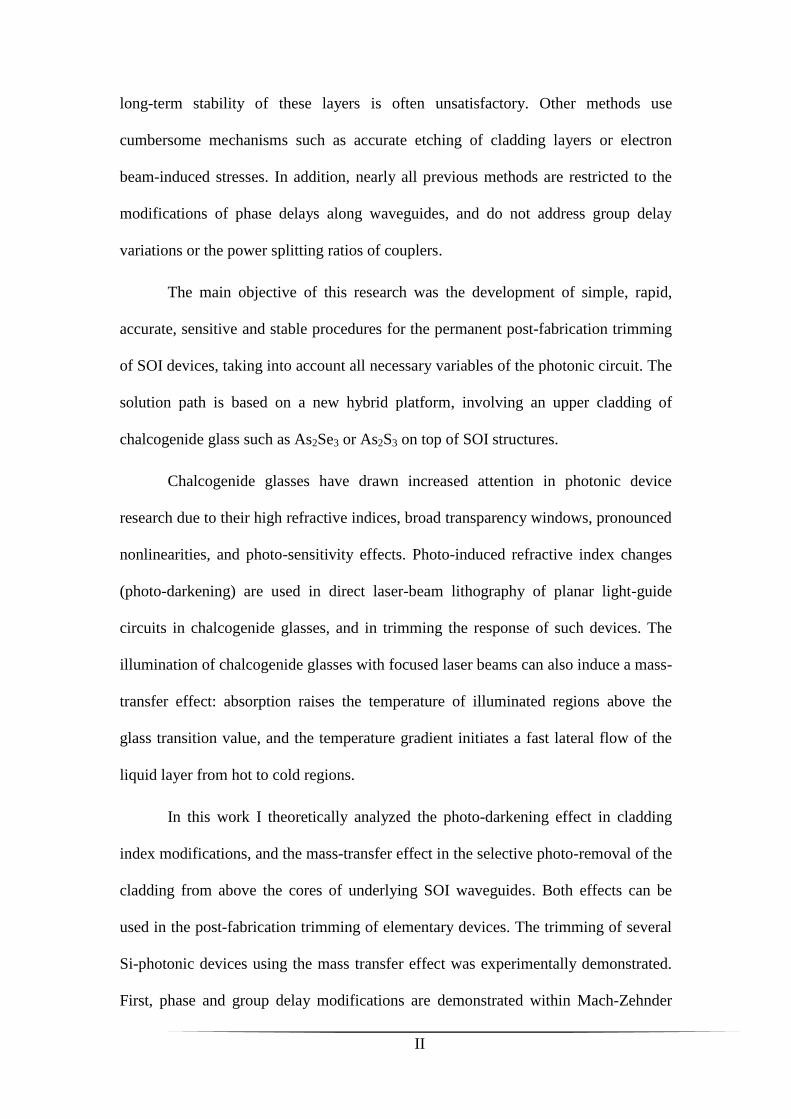
The main objective of this research was the development of simple, rapid,
accurate, sensitive and stable procedures for the permanent post-fabrication trimming
of SOI devices, taking into account all necessary variables of the photonic circuit. The
solution path is based on a new hybrid platform, involving an upper cladding of
chalcogenide glass such as As2Se3 or As2S3 on top of SOI structures.
Chalcogenide glasses have drawn increased attention in photonic device
research due to their high refractive indices, broad transparency windows, pronounced
nonlinearities, and photo-sensitivity effects. Photo-induced refractive index changes
(photo-darkening) are used in direct laser-beam lithography of planar light-guide
circuits in chalcogenide glasses, and in trimming the response of such devices. The
illumination of chalcogenide glasses with focused laser beams can also induce a mass-
transfer effect: absorption raises the temperature of illuminated regions above the
glass transition value, and the temperature gradient initiates a fast lateral flow of the
liquid layer from hot to cold regions.
In this work I theoretically analyzed the photo-darkening effect in cladding
index modifications, and the mass-transfer effect in the selective photo-removal of the
cladding from above the cores of underlying SOI waveguides. Both effects can be
used in the post-fabrication trimming of elementary devices. The trimming of several
Si-photonic devices using the mass transfer effect was experimentally demonstrated.
First, phase and group delay modifications are demonstrated within Mach-Zehnder

III
interferometers (MZIs). Group index modifications by as much as 2% are achieved in
SOI ridge waveguides. Analysis shows that considerably larger variations may be
achieved in fully-etched, rectangular silicon nano-wire waveguides.
Second, the modifications of the power splitting ratios of directional couplers
are demonstrated in tuning the transfer functions of SOI race-track resonators. The
extinction ratios of individual resonances are arbitrarily adjusted between 4- 40 dB.
These variations correspond to changing the coupling coefficient per unit length of the
directional coupler by 10%. Here too, use of fully-etched nano-wires is expected to
enhance the changes in coupling coefficient, up to 45%. Lastly, the tuning platform
was employed in adjusting the response of cascaded MZIs 1x4 and 1x8 channel de-
multiplexers. The response of tuned devices remains stable following three months of
storage.
This dissertation is organized as follows: A general introduction to silicon
photonics, basic components and fabrication limitations is given in Chapter 1.
Relevant literature on currently-available trimming methods is addressed. Background
on chalcogenide glasses and their photo-sensitivity mechanisms is provided in
Chapter 2. Chapters 3 and 4 describe the fabrication processes and the laboratory
setups used throughout this work. Simulation and experimental results for the tuning
of phase delay, group delay, coupling ratios and cascaded devices are described at
length in Chapters 5, 6 and 7. Chapter 8 gives a theoretical analysis of a specific
potential application of precisely-adjusted cascaded MZIs, such as those reported in
this work, in the all-optical realization of the wavelet-packet decomposition.
Concluding discussion and perspectives are provided in Chapter 9.
1
Introduction
1.1 Integrated photonics on silicon: why and where
1.1.1 The need for integrated optics
Since the invention of optical fiber communication in the 70's, optical fibers
has become the world standard for delivering vast amounts of information over long
distances. In those long-haul (80 to 10,000 km) and metro (20 to 80 km) networks, the
bulk of the cost is related to the optical link (fiber deployment and amplifiers), which
is much higher than the cost of the transceivers. Hence, main efforts in these long-
reach networks are focused on increasing performance in terms of higher spectral
efficiency (in bit/s/Hz), and longer reach. In recent years, however, optical links are
starting to replace copper wires in shorter distance communication as well, coming
closer and closer to the home (Fiber to the Home)[1].
In addition, the Smartphone revolution boosted cloud services, such as
Google, Facebook, Waze etc., hosted by huge data centers which become the central
computation platforms used by many millions around the globe. Those data centers
are facing the challenge of communicating massive amounts of data over ultra-short
optical links between racks and server modules. For those short-range networks, the
link becomes inexpensive and transceiver footprint, power consumption and
fabrication simplicity play a major role in decreasing network cost [2]. These provide
the main motivations for bringing down optical communication systems to the chip
level, making them cheaper and more wildly used in personal devices [3].
Another important driving force for integrated photonics is "Moor's law" for
the scaling of micro-electronics processing power. For more than 45 years, Moore's
2
law was a main driving force for the electronics industry. This prediction of Gordon
Moore stated that the number of transistors on a single mainstream chip would double
itself every two years [4]. The number of transistors in a commercial microprocessor
has grown exponentially from 2,300 in the first Intel 4004 (1971) to more than 5.5
billion in the 18-core Xeon Haswell-E5 (2015). While the desired computation
bandwidth inside the processor and the necessary communication bandwidth to the
outside world grow, engineers are struggling to transfer these outstanding amounts of
electronic data over copper wires. Possible solutions rely on parallel processing based
on numerous smaller units, involving optical interconnects within a single chip.
1.1.2 Silicon-on-insulator as a photonic material platform
The motivation for using silicon as the leading material for the implementation
of photonic integrated circuits is driven by the mature semiconductor industry and the
potential for close integration of photonics alongside electronics on the same material
platform [5], [6]. Since the late 1990's the micro-electronics industry had shifted to
the Si-on-Insulator (SOI) substrate as the primary material platform, in place of the
conventional silicon substrate. This shift reduced parasitic devices capacitance, due to
their isolation from bulk silicon, enabling performance improvement [7].
While fully adopted by the electronic industry, the SOI substrate also provides
some important potential advantages for the implementation of photonic integrated
circuits (PICs). On top of mature fabrication using available micro-electronics
industry facilities, and higher integration with electronics, silicon also exhibits useful
optical properties: a broad spectral window of low propagation losses, from 1.1 µm
wavelength up to 7 µm; comparatively tight confinement of the optical mode due to
the high index contrast between Si core and SiO2 cladding; high threshold for optical
3
damage; high thermal conductivity; and high nonlinear index (Kerr effect),which is
100 times larger than that of silica.
Alongside these advantages, the SOI platform also suffers from several
deficiencies from photonics standpoint. One of the major drawbacks is the indirect
bandgap of silicon: the state of maximum energy in the valence band and the state of
minimum energy of the conduction band are associated with very different electron
momentum values. The amplification of light in semiconductor materials involves
stimulated emission processes, which include the transition of an electron from the
valence band to the conduction band, and the generation of an additional photon. The
momentum mismatch in indirect bandgap semiconductors makes these stimulated
transitions highly inefficient. Solutions include hybrid integration of direct-bandgap
III-V layers on top of SOI [8][9], or flip-chip bonding of external laser diodes.
Another significant drawback of silicon is the lack of second order
nonlinearities such as the Pockels effect, which is underlying electro-optic modulation
in LiNbO3, for example [10]. The Pockels effect is practically instantaneous. Instead,
silicon-based modulators rely on the free-carrier dispersion effects, which are
inherently slower. Nevertheless, state-of-the-art silicon modulators reach tens of GHz
rates [11]. The large thermo-optic coefficient of silicon [12], which is useful in
sensors applications, leads to undesired temperature variations of device transfer
functions. The high index contrast between silicon and silica, while providing tight
confinement, also gives rise to losses due to scattering at rough interfaces.
1.2 Passive optical devices and filters in silicon
The SOI platform is being used in the realization of many passive and active
photonic devices, including modulators [13], Si-Ge detectors for optical
communication wavelengths [14], hybrid III-V on SOI light sources, and complex
4
optical filters [15], [16], all of which can be incorporated into communication links as
well as other applications. In this work I focus on our efforts towards silicon-photonic
integrated passive optical filters. These filters are used in the wavelength-division
multiplexing (WDM) and de-multiplexing of communication channels [16], [17],
sensor application [18], [19], radio-frequency (RF) photonics [20], and on-chip signal
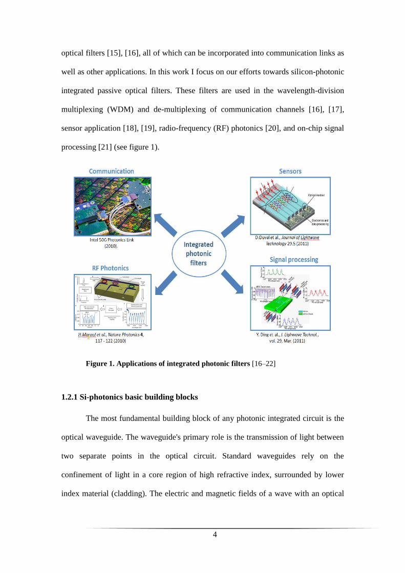
processing [21] (see figure 1).
Figure 1. Applications of integrated photonic filters [16–22]
1.2.1 Si-photonics basic building blocks
The most fundamental building block of any photonic integrated circuit is the
optical waveguide. The waveguide's primary role is the transmission of light between
two separate points in the optical circuit. Standard waveguides rely on the
confinement of light in a core region of high refractive index, surrounded by lower
index material (cladding). The electric and magnetic fields of a wave with an optical

5
frequency , propagating in the positive z direction with a propagation constant ,
can be described by the following equation:
(1) ( , , , ) ( , )exp[ ( ) ]
( , , , ) ( , )exp[ ( ) ]
E x y z t E x y j t j z
H x y z t H x y j t j z
Here and elsewhere overhanging arrows denote vectors, and an overhanging
tilde sign denotes a variable that is changing in time at optical frequencies. ,E H
denote electric and magnetic fields, respectively. One significant property of a mode
propagating in a waveguide is that the z dependence of the field is only in the
accumulation of phase, while the transverse profile ,E x y does not vary with
propagation (more on that later). Both profile and propagation constant are, in
general, wavelength-dependent.
The complete description of the electromagnetic wave propagating along the
structure is given by the solutions of the wave equation, including the boundary
conditions defined by the waveguide structure geometry:
(2) 2 2 2
0 0E n k E ,
Here n denotes the refractive index as a function of position and 0k c .
The wave equation is a representation of Maxwell's equations in dielectric media.
Let us consider first a slab waveguide geometry, which is infinite in both the
propagation direction z as well as in the y direction (figure 2).
6
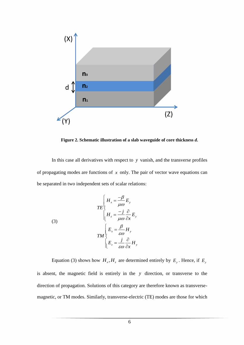
Figure 2. Schematic illustration of a slab waveguide of core thickness d.
In this case all derivatives with respect to y vanish, and the transverse profiles
of propagating modes are functions of x only. The pair of vector wave equations can
be separated in two independent sets of scalar relations:
(3)
x y
z y
x y
z y
H E
TEj
H Ex
E H
TMj
E Hx
Equation (3) shows how ,x zH H are determined entirely by yE . Hence, if
yE
is absent, the magnetic field is entirely in the y direction, or transverse to the
direction of propagation. Solutions of this category are therefore known as transverse-
magnetic, or TM modes. Similarly, transverse-electric (TE) modes are those for which

7
yH vanishes, and consequently the electric field is entirely in the y direction. These
definitions are summarized below:
(4) 0 0,
0 0,
z z
z z
E H TE
H E TM
The transverse profiles of TE modes, for example, may be solved using the
following procedure:
Solving the wave equation for the transverse profile of the scalar field
component yE x . Solutions are either real or imaginary exponential
functions of x .
Since we are interested in propagating mode that are guided within an inner
core layer, the discussion is restricted to those mathematical solutions in which
yE x is oscillating within the core of index 2n , and exponentially decaying
within upper and lower cladding regions of index 1 2n n . This condition
restricts the possible values of the propagation constant: 0 1 0 2k n k n .
The obtained solution is of the form:
(5)
2 2 2 2
2 0 2 0
2 2
1 0
2 2
1 0
sin(( ( ) ) ) cos(( ( ) ) ) ,
( ) exp( ( ( ) ) ),
exp( ( ( ) ) ),
y
A n k x B n k x core
E x C n k x clad
D n k x
,
where , , ,A B C D are constants. These in turn must be determined by the
boundary conditions, which in the TE case require that both yE and zH , (and hence
yE x ), are continuous across the two boundaries between the core and cladding
layers. The obtained set of algebraic equations has a non-trivial solution only for a
8
discrete set of propagation constant values TE
j . Each propagation constant value
completely defines the transverse profile of the field, and hence all properties of an
individual mode. The effective index associated with a mode is defined by:
(6) ,
0
TE
jeff TE
jnk
The number of modes is governed by the following parameter of the
waveguide: 2 2
0 2 1V k d n n , where d is the thickness of the core layer. Most of the
optical waveguides used in communications are single-mode: meaning that they
support only a single TE and a single TM mode. Single-mode operation is
advantageous since the propagation constants of different modes vary considerably
(giving rise to modal dispersion). The condition for a single TE mode in a slab
waveguide is simple: V .
Integrated photonic circuits require a compact and planar waveguide structure.
The high index difference between silicon core (3.48 RIU at 1550 nm) and silica
cladding materials (1.45 RIU) in SOI provides strong confinement of the optical mode
in a sub-micron core region, allows for low loss over tight bending radii, and reduces
footprint. On the other hand, the large index contrast results in higher losses due to
scattering from sidewall roughness, and in stronger chromatic dispersion.
Structures which provide confinement in a single transverse dimension only
are not of much use in integrated devices. Any input beam of finite extent in the y
direction is bound do diffract while propagating in a slab waveguide. Practical devices
employ two-dimensional cross-sections which provide refractive index confinement
in both transverse dimensions.
9
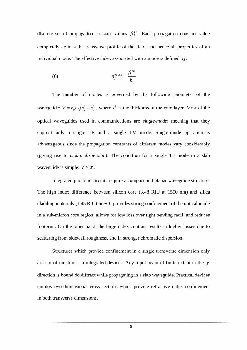
Typical SOI wafers used in photonic devices fabrication have a 220 nm-thick
device layer and a 2 μm-thick buried oxide layer (BOX), attached to a 750 μm-thick
silicon handle layer. There are several widely employed geometrical designs for
waveguide cross sections: the silicon nano-wire, which is a rectangular-shaped silicon
waveguide with typically 500 nm width surrounded by air and a silica lower cladding;
the ridge waveguide, which is generally wider (~700nm width) and only partially
etched and provides lower scattering losses; and the slot waveguide which is a nano-
wire with an etched trench in its center. The transverse modal profile in slot
waveguides in concentrated in the low-index trench between the silicon regions to
both its sides [5]. The three waveguide geometries are shown in figure 3, alongside
numerical COMSOL Multi-Physics calculations of the transverse profiles of their
fundamental modes.
Figure 3. Three Si-photonics waveguides cross-sections: Ridge (left), rectangular
(center) and slot (right).
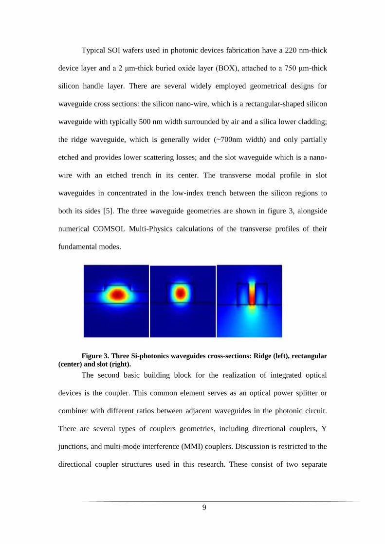
The second basic building block for the realization of integrated optical
devices is the coupler. This common element serves as an optical power splitter or
combiner with different ratios between adjacent waveguides in the photonic circuit.
There are several types of couplers geometries, including directional couplers, Y
junctions, and multi-mode interference (MMI) couplers. Discussion is restricted to the
directional coupler structures used in this research. These consist of two separate
10
waveguide cores in close proximity. The joint cross section supports two fundamental
modes: a symmetric and an anti-symmetric one, as shown in figure 4.
Figure 4. Schematic illustration of a directional coupler (top) with the simulated
transverse profiles of the even (bottom left) and odd (bottom right) optical modes. The
effective indices of both modes are noted as well.
Incident light from each of the cores is split between the symmetric and anti-
symmetric modes of the joint structure, with equal-magnitude projections. The two
hybrid modes are characterized by different propagation constants, leading to length-
dependent interference between the two projections along the coupler, and to a
periodic power transfer between the two cores [23], [24].
The transfer of the optical fields from both inputs to both output ports of a
coupler comprised of two identical waveguides may be described by the transfer
matrix notation of Equation (7):
(7)
1 1
2 2
cos( ) sin( ),
sin( ) cos( )
out in
out in
E Ejz
jE E
.
1
inE
2
inE
k 1
outE
2
outE
2.3953even
effn 2.3849odd
effn
SiO2 SiO2
Air Air
Si Si
11
Here 1,2
inE , 1,2
outE are the input and output fields magnitudes in cores 1 and 2,
and is the coupling coefficient per unit length which may be calculated using a 2D
numerical simulation for the even and odd modes [23]:
(8)
0
even odd
eff effn n
If the separation between waveguide cores is comparatively large, so that the
overlap between the modes of individual waveguides is small (a condition known as
the weak coupling regime), it is possible to obtain an approximation for the coupling
coefficient without solving for the compound structure. The coefficient is given by the
overlap integral between the two modes, weighed over the spatial extent of one of the
cores. For a coupler comprised of two identical waveguides:
(9) * 201 12 2, ( , ) ( , )
4E x y n x y E x y dxdy
Here 2 2 2
12 2 1n n n within a single core, and zero elsewhere.
Using these two elementary building blocks for the guiding and coupling of
light, basic photonic filters may be realized, such Mach-Zehnder interferometers
(MZIs) and ring resonators. Those basic filters, in turn, can be cascaded to achieve
more complex functionalities.
1.2.2 The representation of digital filters in photonic structures
Integrated photonic filters perform a summation of delayed replicas of the
input and /or output signals. In most cases of interest, all delays in the filter are integer
multiples of a basic, unit interval T . In this respect, they are analogous to linear time-
invariant (LTI) digital signal processing (DSP) filters. The transfer functions of such
filters is best described in terms of the Z-transform, which is an extension of the

12
frequency variable f in the discrete time Fourier transform (DTFT) to complex
values z as shown in equation (10):
(10) 2 ( ) 2( ) ( ) ( ) ( )j f nT j f T n
n n
H f h nT e z e H z h nT z
Here h and H denotes the time-domain impulse response and the Z-domain
response of an LTI filter, respectively. The system frequency response is represented
by the values of H on the unit circle in the Z domain. It can be calculated form it's Z
transform by simply placing exp 2z j f .
The output of an LTI digital filter can be expressed as a weighted sum of
delayed inputs ( )x kT and delayed outputs ( )y kT , where k is an integer, through the
difference equation (11):
(11)
0 1
1
( ) ( ) ( 1) ... ( )
( 1) ... ( )
feedforward
M
feedback
N
y nT b x nT b x n T b x n M T
a y n T a y n N T
The corresponding Z-domain transfer function is a ratio of two polynomials,
of the form shown in equation (12):
(12) 0 1
0 1
( )
( )
( )
MMN Mm
mm
m m
N Nn
n p
n n
z z zb z
H z
a z z z
The values mz and
pz in which the numerator and denominator vanish are
known as 'zeros' and 'poles', respectively. The existence of poles represents feedback
paths.
Digital filters can be classified into one of following categories [25]:

13
FIR – finite impulse response filters, also called moving average (MA) filters.
These contain only zeros, and represent sums of weighted replicas of the input signal
without feedback.
IIR – Infinite impulse response filters. These can be split further into two sub-
categories: filters that include only poles are known as auto-regressive (AR) filters,
and those that include both zeros and poles and referred to as auto-regressive moving-
average (ARMA) filters.
Use of the zeros-poles Z-transform representation can reveal some of the basic
properties of filters. The zeros represent the points in the complex Z plane in which
the transmission becomes zero. When the locations of zeros approach the unit circle,
strong suppression of signals at specific frequencies is achieved. The poles are related
to the feedback weights. Therefore, higher poles magnitudes (closer to unity)
represent stronger feedbacks which result in a sharper frequency response. In the
following I present the photonic realization of two fundamental FIR and IIR filters.
1.2.3 Single-stage finite-impulse-response filters
The photonic equivalent of a single-zero MA filter is the MZI. It consists of
two couplers connected by unbalanced waveguides with a differential unit delay , as
shown in figure 5.
Figure 5. Illustration of an integrated-photonic Mach-Zehnder interferometer
1
inE
2
inE
1
outE
2
outE
1k2k
1z
14
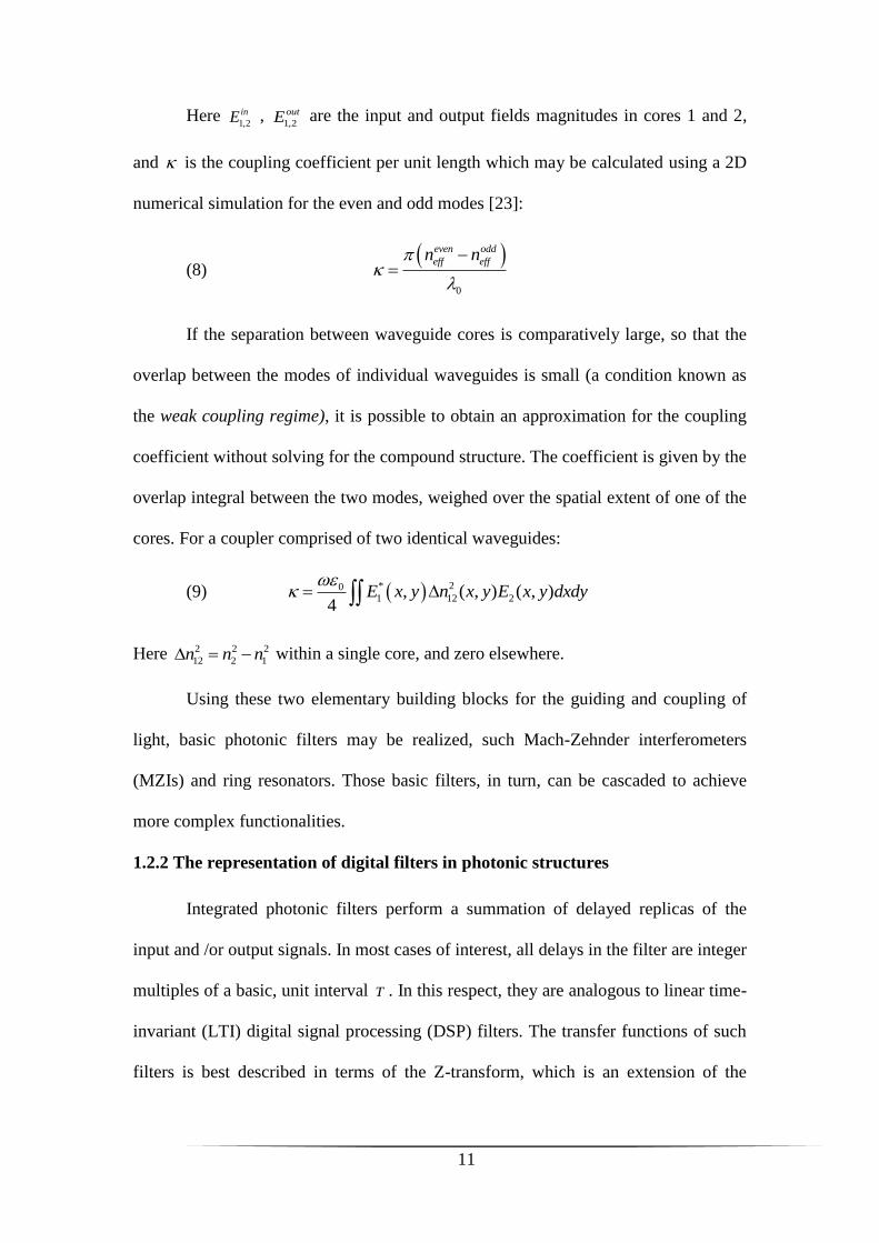
The Z-domain transfer function between the input and output ports of the MZI
can be written by the following matrix equation (13) [25]:
(13)
1 1
1 2 1 2 1 2 1 2
1 1
1 2 1 2 1 2 1 2
( (1 )(1 ) ) , ( 1 1 )
( 1 1 ) , ( (1 )(1 ) )MZI
z j z
j z z
Here 2
1,2 1,2cos are the power splitting ratios of the first and second
couplers, respectively (see equations (7)). Propagation losses along the waveguides
connecting the two couplers were neglected in Eq. (13) (see below). Figure 6 shows a
simulated transmission spectrum of a SOI MZI with a 1 mm-long delay imbalance.
Both couplers within the MZI have power splitting ratios of 50%.
Figure 6. Simulated power transfer function of a silicon-photonic MZI with a
differential path imbalance of 1 mm, and two couplers of 50% power splitting ratios.
The extinction ratio of a device transfer function is defined as the difference in
dB scale between maximum and minimum power transmission. This parameter
quantifies, for example, how well certain wavelengths are blocked in a filter. The
extinction ratio in a simple MZI depends on the amplitudes of the two interfering
waves in the output port. When the incoming waves have equal amplitudes, large
1548 1549 1550 1551 1552-30
-25
-20
-15
-10
-5
0
5FSR=0.6445nm
tra
nsm
issio
n[d
b]
[nm]
15
extinction ratios are obtained as the two waves perfectly cancel out each other at when
interfered destructively. Unequal amplitudes degrade the extinction ratio. The
amplitudes at the output ports depend on both power splitting ratios in the directional
couplers and on losses along the MZI optical paths.
In devices made with a short differential delay, and/or made of low-loss
waveguides, propagation loss does not play a role and optimum extinction ratio is
achieved with 50% couplers. Large propagation losses require that the splitting ratio
of the first coupler is modified to launch more power into the longer, lossy arm of the
MZI. The second, output coupler remains balanced at 50% ratio.
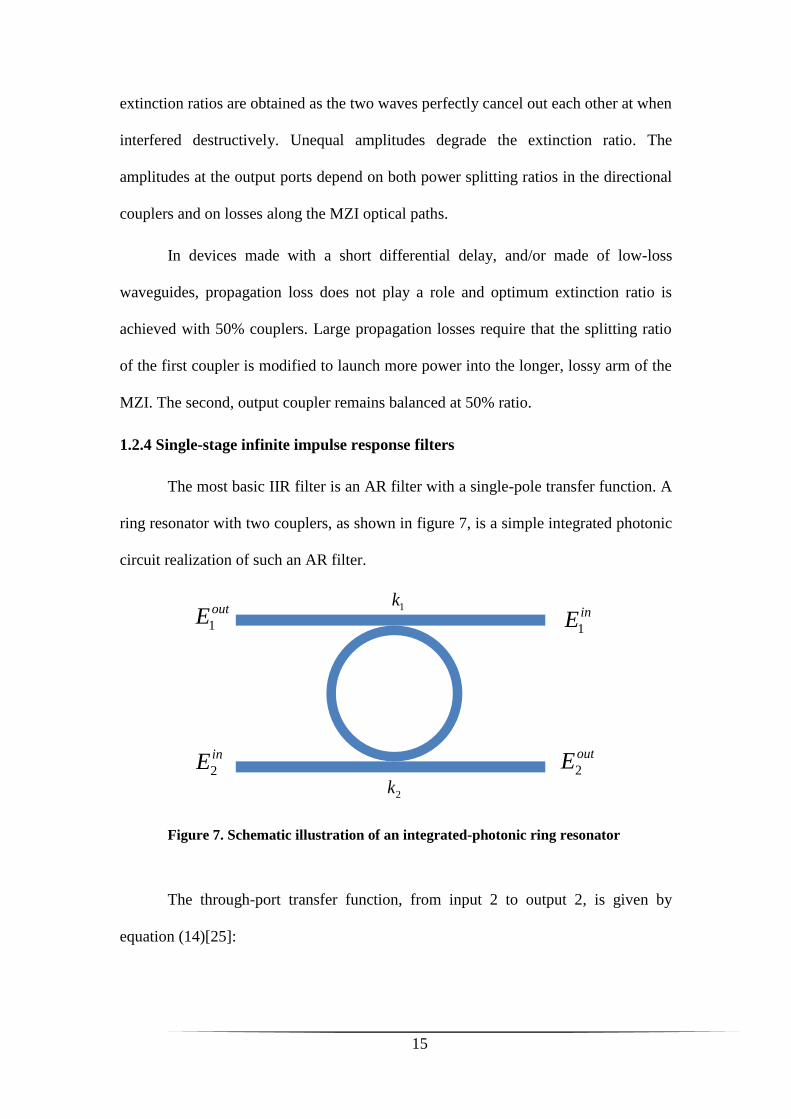
1.2.4 Single-stage infinite impulse response filters
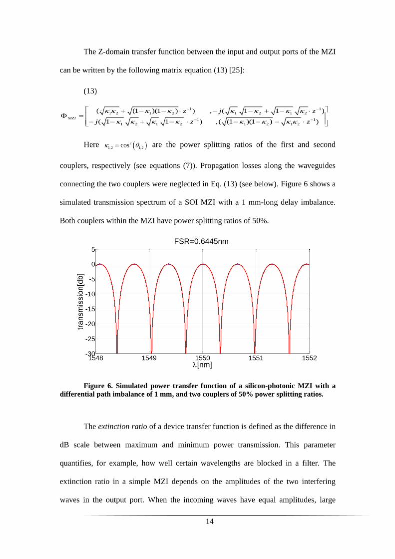
The most basic IIR filter is an AR filter with a single-pole transfer function. A
ring resonator with two couplers, as shown in figure 7, is a simple integrated photonic
circuit realization of such an AR filter.
Figure 7. Schematic illustration of an integrated-photonic ring resonator
The through-port transfer function, from input 2 to output 2, is given by
equation (14)[25]:
1
inE1
outE
2
inE 2
outE
1k
2k
16
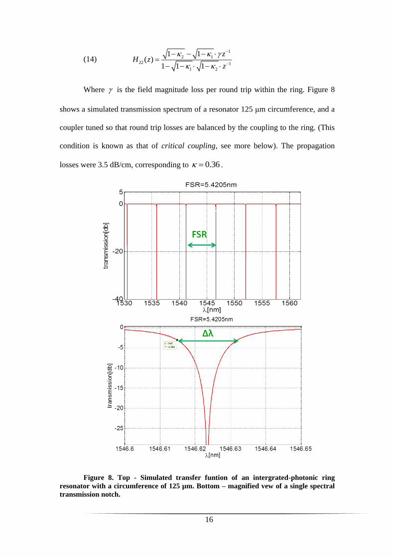
(14) 1
2 1
22 1
1 2
1 1( )
1 1 1
zH z
z
Where is the field magnitude loss per round trip within the ring. Figure 8
shows a simulated transmission spectrum of a resonator 125 μm circumference, and a
coupler tuned so that round trip losses are balanced by the coupling to the ring. (This
condition is known as that of critical coupling, see more below). The propagation
losses were 3.5 dB/cm, corresponding to 0.36 .
Figure 8. Top - Simulated transfer funtion of an intergrated-photonic ring
resonator with a circumference of 125 µm. Bottom – magnified vew of a single spectral
transmission notch.
17
The transfer function of ring resonators is often quantified in terms of the
following parameters:
FSR- Free Spectral Range: the wavelength separation between two adjacent
peaks (or notches) in the transmission spectrum of the resonator. The FSR is
determined by the propagation delay within the ring cavity, and is defined by [25]:
(15) 2
0
2 g
FSRn l
.
Here 0 , ,gn l are the peak transmission wavelength, the group delay index along the
resonator waveguide, and the cavity physical length.
Critical coupling – A specific value of the coupling coefficient into the ring,
for which the transfer of power to the through port at resonance wavelengths is
exactly zero. At critical coupling, the influx of electrical field into the ring through the
input port is cancelled by the overall roundtrip losses. The numerator of Eq. (14)
vanishes at this condition. For resonators with only a single input / output coupler (
1 0 ), critical coupling implies that 21 .
Quality factor- (Q factor) is a dimensionless parameter that describes the
sharpness of spectral transmission (or rejection) bands [25]. A higher Q indicates a
lower rate of energy loss within the cavity. High values of Q are also associated with
narrow transmission notches: low losses suggest that light is allowed to propagate
many times within the resonator, achieving better wavelength discrimination. High-Q
resonators are therefore instrumental in filtering, sensing and signal-processing
applications. The definitions for Q found in literature relates wavelength to
bandwidth[26]:
18
(16) 0Q
,
where is the full width at half maximum (FWHM) of a spectral transmission
feature.
Finesse- this quantity relates the FSR to the FWHM [26]:
(17) 0
FSR FSR QF
The cascading of MZI and ring resonator basic filters gives rise to more
complex transfer functions, containing multiple zeros and poles. Advanced algorithms
for the synthesis of such complex filters in the Z domain appear in the literature [25].
Exact amplitudes and phases of zeros and poles locations determine the transfer
function of complex filters. From the optical standpoint, changes to the optical
properties of basic building blocks, such as phase accumulation along waveguides or
splitting ratios of directional couplers, would modify the functionalities of filters
entirely.
1.2.5 High-end Si photonics filters integration
In recent years, the outcome of research in Si-photonics technology is
beginning to penetrate into industrial applications, while more advanced academic
works continue to realize cascaded passive and active components with ever-
increasing levels of complexity and integration on a single chip. In one example, a
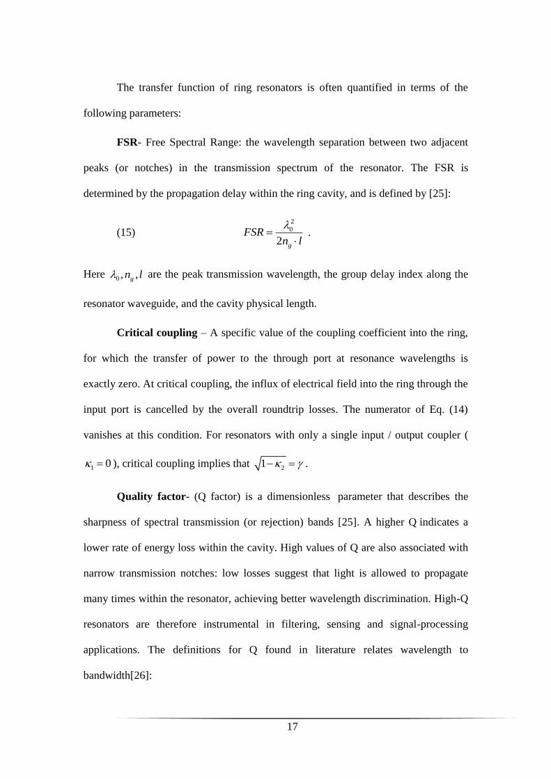
4x10 Gbit/s transceiver was fabricated by Luxtera on a single chip platform, including
flip-chip bonded lasers, Si MZI modulators, silicon WDM filters and Si-Ge
photodetectors (figure 9,[27], [28]).
19
Figure 9. Luxtera 4x10 Gbit/s full tranciever on single chip, using Si-photonics
technology [27], [28].
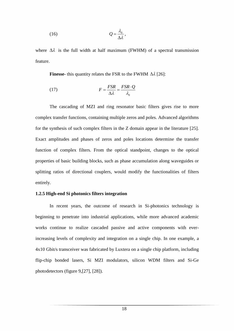
In another example, Kotura demonstrated a VOA based on Si photonics
technology and hardware aiming to a 100 Gbit/s WDM link on a chip, using Si-
photonics technology [29], [30] (figure 10),).
Figure 10. Kotura 100Gbit/s WDM transmitter and receiver modules, based on
Si-photonics technology [29], [30].
20
The advances in fabrication methods of Si-photonics in recent years enable the
realization of complex filter structures. For example, a ultra-compact, high-order
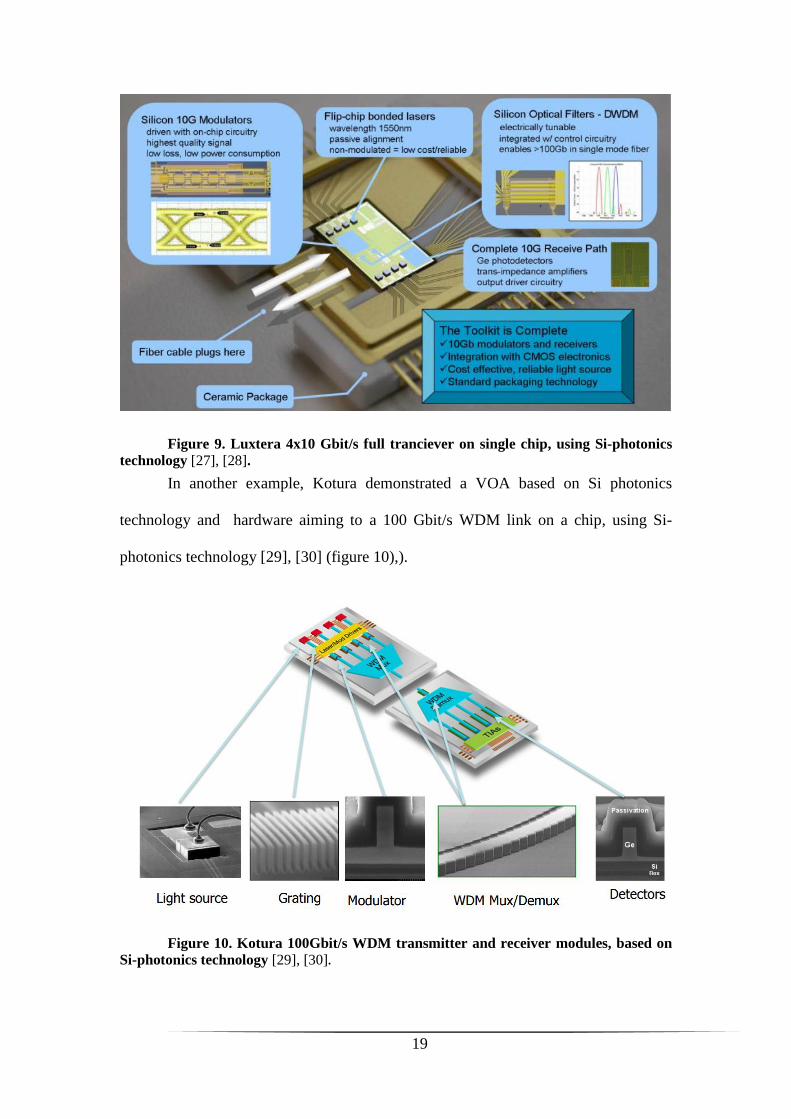
photonic filter on silicon, containing five cascaded ring resonators, was developed by
IBM research labs (figure 11, [31]). The multiple-pole structure provides strong out-
of-band attenuation, a flat pass-band, and sharp spectral transitions. These filters are
applicable to WDM channel multiplexing in all-optical inter-connects.
Figure 11. Left - SEM image of an ultra-compact, sharp photonic filter
containing five cascaded ring resonators, fabricated by IBM labs [31]. Right –
meassured power transfer functions of devices with three and five cascaded rings.
1.3 Si-photonics fabrication tolerances
The transfer functions of all real-world photonic filters are susceptible to
inaccuracies resulting from inevitable fabrication tolerances. Tolerances affect the
waveguide cross section dimensions and the optical paths lengths. Small-scale cross
section geometry inaccuracies, for example, modify the effective index of the
waveguide and introduce random phase delay variations that accumulate over long
waveguides.
21
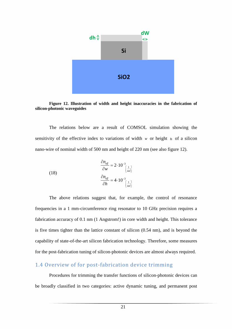
Figure 12. Illustration of width and height inaccuracies in the fabrication of
silicon-photonic waveguides
The relations below are a result of COMSOL simulation showing the
sensitivity of the effective index to variations of width w or height h of a silicon
nano-wire of nominal width of 500 nm and height of 220 nm (see also figure 12).
(18)
3
1
3
1
2 10
4 10
eff
nm
eff
nm
n
w
n
h
The above relations suggest that, for example, the control of resonance
frequencies in a 1 mm-circumference ring resonator to 10 GHz precision requires a
fabrication accuracy of 0.1 nm (1 Angstrom!) in core width and height. This tolerance
is five times tighter than the lattice constant of silicon (0.54 nm), and is beyond the
capability of state-of-the-art silicon fabrication technology. Therefore, some measures
for the post-fabrication tuning of silicon-photonic devices are almost always required.
1.4 Overview of for post-fabrication device trimming
Procedures for trimming the transfer functions of silicon-photonic devices can
be broadly classified in two categories: active dynamic tuning, and permanent post
Si
SiO2
dWdh
22
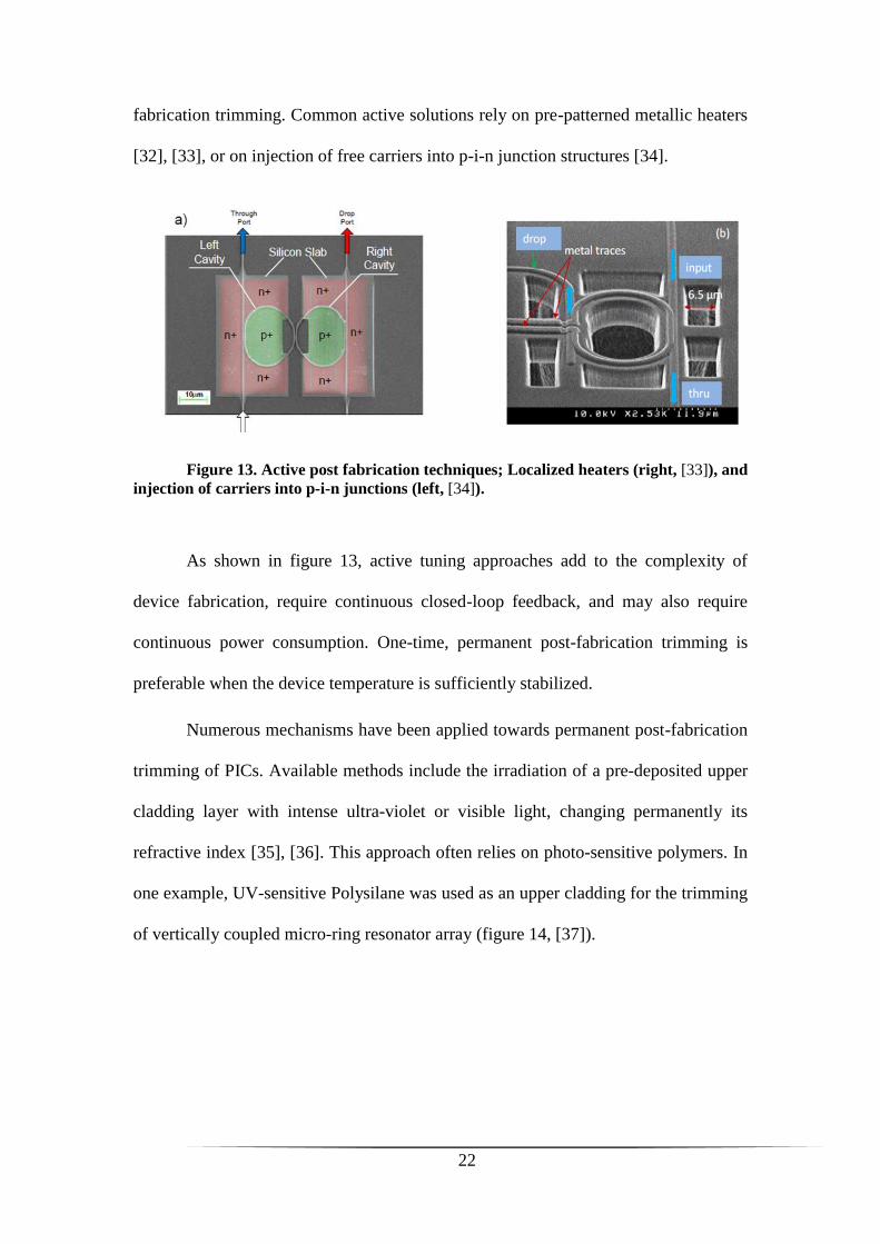
fabrication trimming. Common active solutions rely on pre-patterned metallic heaters
[32], [33], or on injection of free carriers into p-i-n junction structures [34].
Figure 13. Active post fabrication techniques; Localized heaters (right, [33]), and
injection of carriers into p-i-n junctions (left, [34]).
As shown in figure 13, active tuning approaches add to the complexity of
device fabrication, require continuous closed-loop feedback, and may also require
continuous power consumption. One-time, permanent post-fabrication trimming is
preferable when the device temperature is sufficiently stabilized.
Numerous mechanisms have been applied towards permanent post-fabrication
trimming of PICs. Available methods include the irradiation of a pre-deposited upper
cladding layer with intense ultra-violet or visible light, changing permanently its
refractive index [35], [36]. This approach often relies on photo-sensitive polymers. In
one example, UV-sensitive Polysilane was used as an upper cladding for the trimming
of vertically coupled micro-ring resonator array (figure 14, [37]).

23
Figure 14. Trimming of the transfer function of a micro-ring array using the
irradiation of an upper cladding layer of a UV-sensitive polymer [37].
In another example, photo-induced stresses and photo-elasticity were
introduced by electron-beam irradiation of a silica over-layer, to modify the effective
index of an underling Si waveguide (figure 15, [38]). Other methods include use of
liquid crystals [39], patterning of a thin, upper silicon nitride film [40], and local
oxidation of the surface of silicon [41].
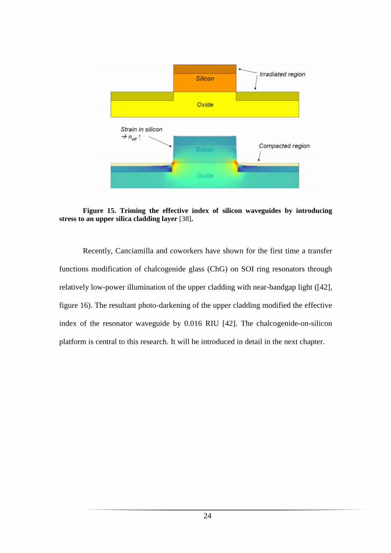
24
Figure 15. Triming the effective index of silicon waveguides by introducing
stress to an upper silica cladding layer [38].
Recently, Canciamilla and coworkers have shown for the first time a transfer
functions modification of chalcogenide glass (ChG) on SOI ring resonators through
relatively low-power illumination of the upper cladding with near-bandgap light ([42],
figure 16). The resultant photo-darkening of the upper cladding modified the effective
index of the resonator waveguide by 0.016 RIU [42]. The chalcogenide-on-silicon
platform is central to this research. It will be introduced in detail in the next chapter.

25
Figure 16. Trimming the response of a silicon-photonic ring resonator through
illuminating an upper layer of chalcogenide glass [42].
Most previously reported methods employ relatively complicated setups or
procedures, require a long process, or involve unstable organic polymer materials that
degrade over time. In addition, most published works only deal with comparatively
small phase delay modifications, whereas trimming of the group delay and directional
couplers are not often addressed.
In this research I try to go beyond what was previously reported using the
ChG-on-SOI material system. By applying a different photo-sensitivity mechanism in
ChG, larger modifications of the effective index can be achieved. The proposed new
method provides a fast, permanent trimming solution for all basic properties of the
integrated-photonic building blocks: phase and group delays along individual
waveguides and the power coupling ratios of directional couplers, all in a single,
simple setup.
26
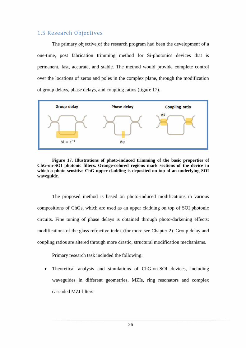
1.5 Research Objectives
The primary objective of the research program had been the development of a
one-time, post fabrication trimming method for Si-photonics devices that is
permanent, fast, accurate, and stable. The method would provide complete control
over the locations of zeros and poles in the complex plane, through the modification
of group delays, phase delays, and coupling ratios (figure 17).
Figure 17. Illustrations of photo-induced trimming of the basic properties of
ChG-on-SOI photonic filters. Orange-colored regions mark sections of the device in
which a photo-sensitive ChG upper cladding is deposited on top of an underlying SOI
waveguide.
The proposed method is based on photo-induced modifications in various
compositions of ChGs, which are used as an upper cladding on top of SOI photonic
circuits. Fine tuning of phase delays is obtained through photo-darkening effects:
modifications of the glass refractive index (for more see Chapter 2). Group delay and
coupling ratios are altered through more drastic, structural modification mechanisms.
Primary research task included the following:
Theoretical analysis and simulations of ChG-on-SOI devices, including
waveguides in different geometries, MZIs, ring resonators and complex
cascaded MZI filters.

27
Evaluation of effective index, group index and coupling ratio variations that
can be achieved using each trimming method.
The establishment of an in-house fabrication procedure within the BIU clean-
room facilities, and joint work with an industrial foundry (TowerJazz) for the
fabrication of complex cascaded Si-photonic devices based on our designs.
Design and assembly of optical trimming and characterization setups
Experimental demonstration of the post-fabrication tuning of MZIs, ring
resonators, and cascaded MZIs.
28
The chalcogenide glass on silicon photonic platform
2.1 What are chalcogenide glasses?
Glasses in general are non-crystalline solids which can be described as a
separate discipline in solid state physics. Glasses can be divided into several different
groups, among them we find the common oxide-based glasses, fluorides, metal-based
glasses and chalcogenides [43]. Chalcogenide glasses (ChGs) contain one or more of
the chalcogen elements from group 6a of the periodic table: sulfur, selenium or
tellurium [44], [45]. The term "chalcogens" was derived from the Greek word
chalcos, meaning "ore formers," since they are found as copper ores. Their
compounds are referred to as "chalcogenides." The semi-conducting properties of the
ChGs were discovered in 1955 by Kolomiets and Golunova from Ioffe Institute in
Leningrad [45]. This discovery led to much research and many applications, such as
in re-writable discs and non-volatile memory devices.
Many of the unique properties of ChGs result from chemical bonds that form
amorphous networks among atomic constituents. Pure ChGs often exhibit ageing
effects [46]. In order to avoid those drawbacks, additional elements are added to the
glass matrix including Ge, Bi, As, etc. Such ChG compositions are characterized by a
higher melting temperature and better stability [46]. Amorphous ChG films often
consist of many single layers one on top of each other, each sheet containing the basic
elements of the glass with the right stoichiometry, connected to each other by a
network of covalent bonds as can be shown in figure 18.

29
Figure 18. Illustration of the amorphous structures of chalcogenide glass films
[47].
In the last decades, the optical properties of ChGs have been extensively
explored. Their compositions include heavy atoms, which lower their vibration
energies and make them transparent in the infrared (IR) range: up to 11 µm
wavelength for sulfur compounds, and up to 15 µm and even 20 µm in certain Se- and
Te-based compounds, respectively. This intrinsic transparency window, which
includes much of the molecular fingerprint region of 2 – 25 µm, makes ChGs
attractive for use in IR spectroscopy, imaging and sensors [48].
In addition, densities of ChGs are higher than those of oxide glasses, and they
exhibit strong polarizabilities and high linear refractive indices (up to 3.5 RIU). This
also implies a large non-linear index, according to Miller's rule [49]. The high non-
linear index is often accompanied by weak two-photon absorption (TPA) at
telecommunication wavelengths, due to the broad transparency window.
Chalcogenide glasses are therefore a favorable platform for nonlinear all-optical
signal processing applications [50].
In recent years waveguides in a thin chalcogenide glass films gain popularity.
A higher intensity (power per unit area) can be achieved in small core waveguides,
better exploiting nonlinear effects. The thin ChG films are produced by thermal
30
evaporation [51], sputtering [52], chemical vapor deposition [53] and pulsed laser
deposition [54]. Several methods had been demonstrated towards the patterning of rib
or ridge waveguide profiles. In direct writing [55–58], for example, the illumination
of As2S3 films at fluencies of around 100 J cm–2
at 514 nm or 532 nm typically results
in an index change of ~0.04 at 1550 nm. This index change is sufficient to inscribe
single-mode waveguides with cores that are a few µm wide, but can be unstable when
heated or exposed to intense irradiation.
Waveguide cores can also be defined based on lithography and etching. These
might be susceptible to sidewall roughness-induced losses following the etching
process, however extremely low losses had been achieved in a series of works by
Madden and coauthors [59]. A third method involves the imprinting of the device
structure into the ChG layer using a mold inside a furnace atmosphere. Low-loss
waveguides and high-Q ring resonators had been reported using this technique [60].
2.2 Photo-induced effects in chalcogenide glasses
One of the most striking properties of ChGs is their photosensitivity: the
changes in chemical bonds following the absorption of band-edge light [61].
Absorption creates electron-hole pairs and produces coordination defect states that are
physically close to each other. The defect states might annihilate, returning to either
the original bonding configuration or to a different one [61]. Such bond switching by
illumination can result in macroscopic changes in the physical properties of the
material, which manifest in a broad range of phenomena.
In general, photo-induced modifications observed in chalcogenide glasses can
be classified into few groups and sub-groups[62]. The primary division distinguishes
between effects that are directly related to light and those that are caused by the
heating that is associated with absorption. Examples of the former include photo-
31
darkening [63], photo-induced anisotropy [64], photo-induced photoconductive
changes [65], photo-induced fluidity and phot-induced structural changes [66], as well
as vectorial effects such as photo-induced birefringence [67]. In processes of the latter
category heat, generated through non-radiative recombination of photo-excited
carriers, triggers structural changes. A widely known and employed example is the
phase change between crystalline and amorphous states of ChG glasses, which is used
in erasable optical memories [68]. In the following, a detailed description of the
photo-darkening and mass-transfer structural changes effects is given, due to their
significance in this research.
2.2.1 Photo-darkening
Among the photo-induced changes in ChG glasses, photo-darkening / photo-
bleaching associated with a red / blue shifts of the fundamental absorption edge when
illuminated with bandgap light is the most familiar phenomenon. In addition to
changes in absorption, modifications to the index of refraction of the glass as a
function of frequency also appear, as expected from the Kramers-Kronig relations
[69–71]. These changes may be reversed partially or completely through a simple
annealing process around the glass transition temperature [48]. The effect is
pronounced in most As/Ge based ChG glasses compositions, to a varying degree [63].
The physical mechanisms responsible for the process are still under study. The photo-
induced index changes are useful for the fabrication of optical structures in bulk
glasses and in thin films [72–74] (see illustration in figure 19).

32
Figure 19. Illustration of the definition of a waveguide core through a photo-
darkening effect
2.2.2 Photo-induced mass transfer
Photo-induced changes to ChGs can go beyond index modification.
Illumination with an intense and focused beam may also lead to structural
modifications, as illustrated in figure 20.
Figure 20. Illustration of the photo-induced mass transfer effect
Mass-transfer effects occur due to viscous flow in the glass: absorption raises
the temperature of illuminated regions above the glass transition temperature. This

33
temperature is related to the magnitude of cohesive forces within the glass network,
which must be overcome to allow atom movements. The spatial gradient in
temperature in the illuminated regions initiates a fast lateral flow of the liquid layer,
from hot to cold regions [75]. This effect has been used in the fabrication of Bragg
gratings using a laser interference pattern [75].
2.3 Chalcogenide glass as an upper cladding of silicon-
photonic devices
Both photosensitivity mechanisms discussed above, photo-darkening and
photo-induced mass transfer, can be applied to the post-fabrication trimming of Si-
photonic integrated circuits. The idea is based on the interaction between the guided
light in the silicon waveguide core and an upper ChG cladding. In most waveguide
designs the majority of light is guided in the core area. However, a finite fraction of
the modal profile penetrates into the cladding. Therefore, photo-induced
modifications to the optical and structural properties of an upper cladding layer would
cause a change in the effective index of the guided mode.
The two effects are complementary. Photo-darkening is applicable to fine-
tuning of the effective index and control of phase delays, whereas mass-transfer and
structural changes are suitable for more drastic variations, affecting group delays and
coupling ratios. A different ChG composition is chosen for the implementation of
each effect. As2S3 was selected for photo-darkening-based tuning, due to its large
photo-induced index modifications of up to 0.1 RIU [76]. Mass-transfer was applied
to As10Se90, since the dilution of As in the Se ChG matrix lowers the glass transition
temperature (380 K as opposed to 460 K in As2Se3 [77], [78]), and results in weaker
covalent bonds.

34
Fabrication procedures
This chapter is dedicated to the fabrication process of our ChG-on-SOI
devices. The main phases of the process are described in figure 21 below.
Figure 21. Process flow of chalcogenide glass-on-SOI devices.
The detailed description of the process will be given in two main parts:
fabrication of the basic SOI devices (section 3.1) and of the top ChG cladding (3.2).
In addition, the packaging technique of our devices will be presented as well (3.3).
3.1 Si-Photonics device fabrication
Most of the Si-photonic devices in this research were fabricated using an in-
house process, that had been developed by our group and collaborators in the BIU
Nano-Technology Institute facilities. In the later stages of the study a collaboration
with the industrial silicon fab Tower-Jazz enabled the design and fabrication of more
complex cascaded photonic circuits. In the following a detailed description of the in-
house fabrication process is given.
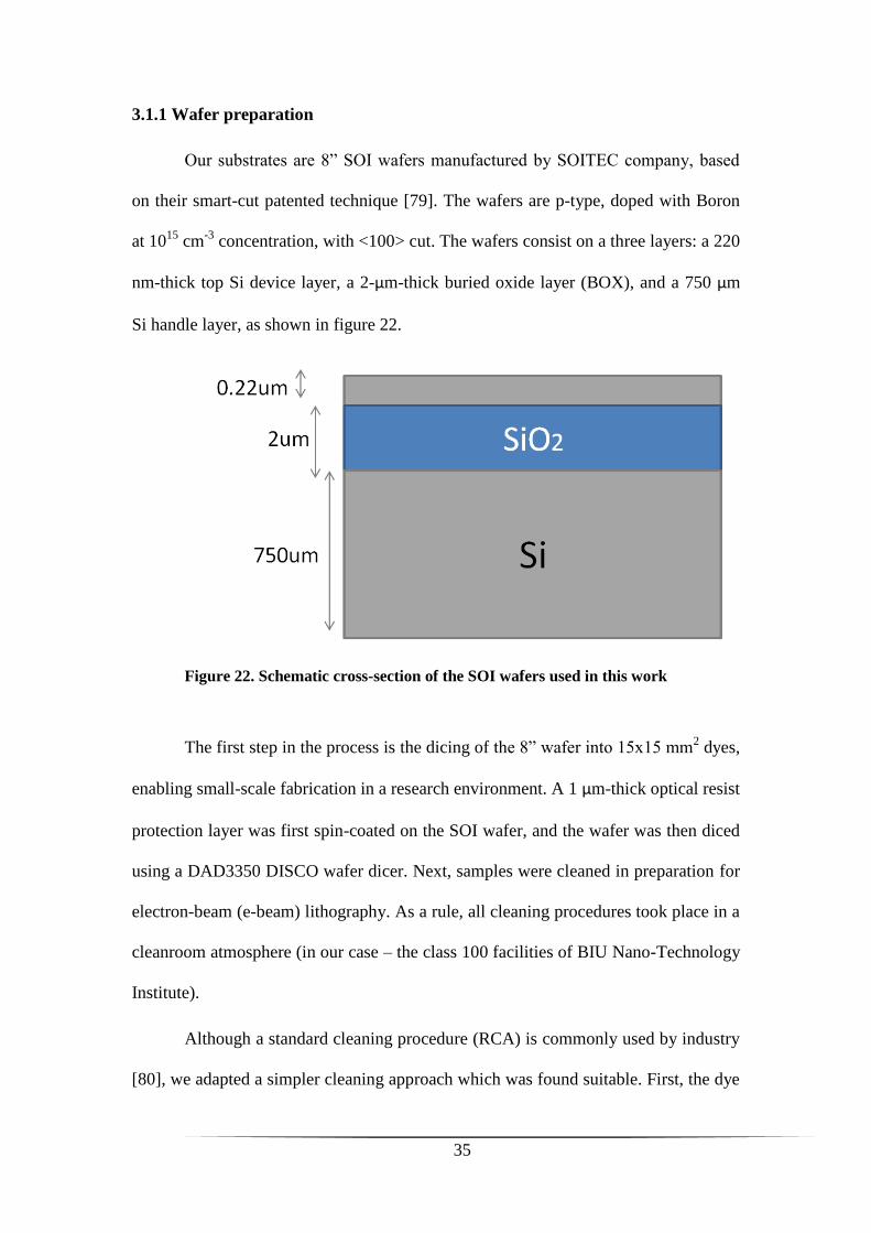
35
3.1.1 Wafer preparation
Our substrates are 8” SOI wafers manufactured by SOITEC company, based
on their smart-cut patented technique [79]. The wafers are p-type, doped with Boron
at 1015
cm-3
concentration, with <100> cut. The wafers consist on a three layers: a 220
nm-thick top Si device layer, a 2-µm-thick buried oxide layer (BOX), and a 750 µm
Si handle layer, as shown in figure 22.
Figure 22. Schematic cross-section of the SOI wafers used in this work
The first step in the process is the dicing of the 8” wafer into 15x15 mm2 dyes,
enabling small-scale fabrication in a research environment. A 1 µm-thick optical resist
protection layer was first spin-coated on the SOI wafer, and the wafer was then diced
using a DAD3350 DISCO wafer dicer. Next, samples were cleaned in preparation for
electron-beam (e-beam) lithography. As a rule, all cleaning procedures took place in a
cleanroom atmosphere (in our case – the class 100 facilities of BIU Nano-Technology
Institute).
Although a standard cleaning procedure (RCA) is commonly used by industry
[80], we adapted a simpler cleaning approach which was found suitable. First, the dye

36
was immersed in acetone and inserted into a sonication chamber for five minutes (30
kHz and 30% power rate). Next, manual surface cleaning by a wipe stick was carried
out to remove any residues from the protective resist. The process was then repeated
with isopropanol as the solvent liquid, eliminating any evaporation residues from the
chip surface.
3.1.2 Electron-beam lithography
The second phase in the process is electron-beam writing. In this stage a high-
resolution, predesigned pattern is imprinted on a special polymer using a scanning
electron beam. First a ZEP-520A e-beam resist from Zion was spin-coated on the SOI
dye, using a Suss MicroTec Delta 6RC Spinner. The ZEP resist is characterized by a
high sensitivity to the writing beam, and shows high resistance to plasma etching with
a selectivity of (1:1) compared to that of Si. The etching of Si to a depth of 220-240
nm requires a 300 nm-thick resist layer. Based on the ZEP-520A datasheet, a spinning
recipe at 4,000 rounds per minute (RPM) for 60 s was chosen, followed by a 3 min of
baking on a hot plate at 180 C.
The next step was the patterning of the waveguide geometry into the electron-
beam resist using a high resolution e-beam lithography writer. In this work patterns
were made using the CRESTEC 9000C EBL system. The writing parameters are
summarized in table 1. The waveguide layouts were drawn by commercial „Adobe
Sketchup‟ drawing program (*.dxf file), and converted into the dedicated CABEL
software of the e-beam system. A minimal field length of 60 µm was chosen, to
reduce discontinuities (stitching) that may occur when the e-beam motorized stage
moves between adjacent fields in the writing process.

37
Parameter Value
Field size 60 µm
Number of dots 20,000 dots per field length
Acceleration voltage 50 kV
Writing current 100 pA
Dose 0.1[
sec
dot
]
ZEP-520A sensitivity 133 µC/cm2
Table 1. Summary of E-beam lithography parameters
Following the writing process, a developer is applied in order to remove the
resist from the irradiated areas. Development was done by immersing the sample in
ZED developer for 35 s, following by 30 s in isopropanol that acts as a stopper, and
drying the sample under nitrogen flow.
3.1.3 Reactive ion etching
In order to transfer the written pattern to the Si device layer, a dry plasma
etching process is undertaken. In this stage a RIE-ICP VERSALINE machine by
PLASMATHERM was used. To accurately etch thin Si layers with vertical sidewall
patterns, a directional ion etching method and a dedicated Si slow-etch recipe were
established and carefully calibrated. The process parameters are summarized in table
2. Following etching, resist leftovers are removed by immersing the dye in NMP
striper for 5 min in a sonication chamber, followed by 1 min of immersion in
deionized water that act as a stopper.
38
Parameter Value
Gas pressure 37.5 µPa
SF6 gas flow 65 ccm
CHF8 gas flow 10 ccm
Chuck temperature 25 C
RIE RF power 100 W
Si Etching rate 3.82 nm/s
Table 2. Summary of reactive ion etching recipe parameters
3.2 Fabrication of chalcogenide glass upper cladding
As mentioned in the previous chapter, two ChG compositions were used as top
cladding layers on top of the Si waveguides: As2S3 for using the photo-darkening
effect and As10Se90 for mass-transfer. The fabrication process of the ChG top cladding
includes three stages, as described in the lower part of figure 17: Photolithography,
ChG deposition and lift-off procedure.
3.2.1 SiO2 buffer layer evaporation
The direct evaporation of both types of ChGs directly on the Si waveguides
resulted in large excess transmission losses. The loss mechanism is not fully
understood at this stage. We suspect that bubbles may be formed at the interface
between glass and waveguide, or that charges remain trapped at the surface. This
issue requires further investigation. Use of a thin SiO2 buffer layer at the interface
between the two materials was found to reduce losses dramatically, depending on its
thickness. On the other hand, a thick buffer layer reduces the modal confinement to
the upper cladding and compromises photo-induced changes to the effective index.
An optimum thickness of 50 nm was chosen. SiO2 was evaporated using an SBT ion-
beam sputtering chamber system, at a vacuum of 9 µPa and a rate of 0.03 nm/s. To
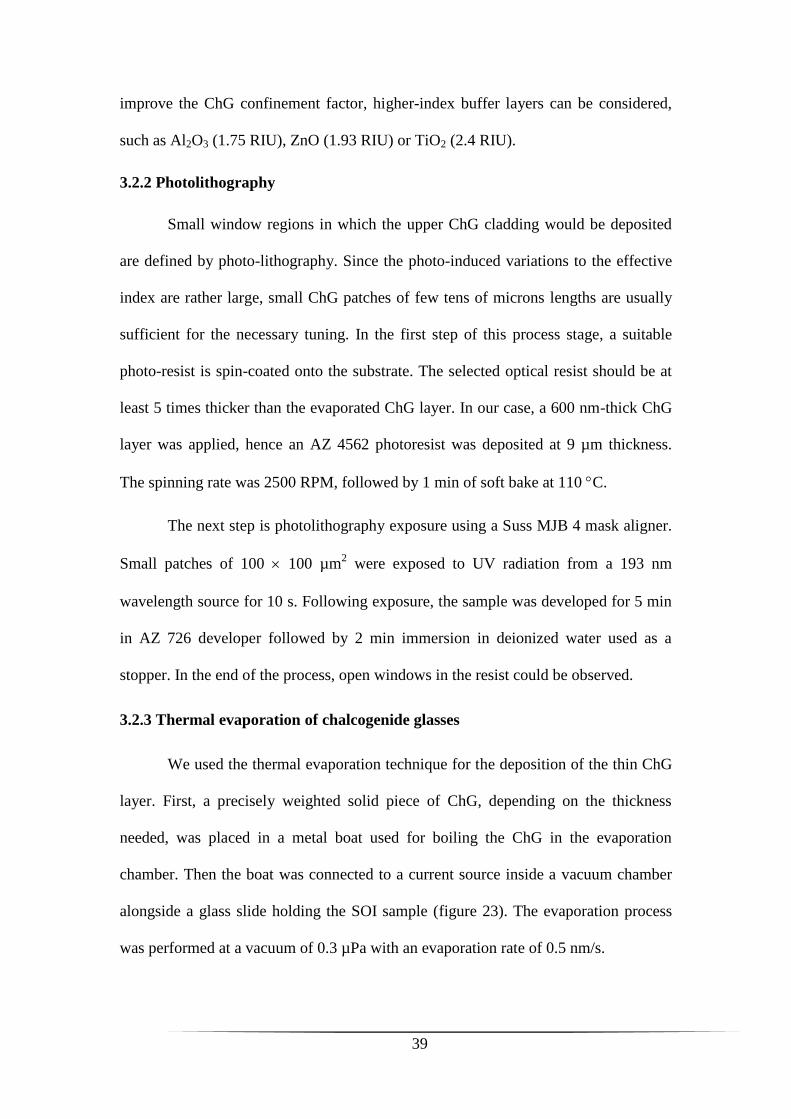
39
improve the ChG confinement factor, higher-index buffer layers can be considered,
such as Al2O3 (1.75 RIU), ZnO (1.93 RIU) or TiO2 (2.4 RIU).
3.2.2 Photolithography
Small window regions in which the upper ChG cladding would be deposited
are defined by photo-lithography. Since the photo-induced variations to the effective
index are rather large, small ChG patches of few tens of microns lengths are usually
sufficient for the necessary tuning. In the first step of this process stage, a suitable
photo-resist is spin-coated onto the substrate. The selected optical resist should be at
least 5 times thicker than the evaporated ChG layer. In our case, a 600 nm-thick ChG
layer was applied, hence an AZ 4562 photoresist was deposited at 9 µm thickness.
The spinning rate was 2500 RPM, followed by 1 min of soft bake at 110 C.
The next step is photolithography exposure using a Suss MJB 4 mask aligner.
Small patches of 100 100 µm2 were exposed to UV radiation from a 193 nm
wavelength source for 10 s. Following exposure, the sample was developed for 5 min
in AZ 726 developer followed by 2 min immersion in deionized water used as a
stopper. In the end of the process, open windows in the resist could be observed.
3.2.3 Thermal evaporation of chalcogenide glasses
We used the thermal evaporation technique for the deposition of the thin ChG
layer. First, a precisely weighted solid piece of ChG, depending on the thickness
needed, was placed in a metal boat used for boiling the ChG in the evaporation
chamber. Then the boat was connected to a current source inside a vacuum chamber
alongside a glass slide holding the SOI sample (figure 23). The evaporation process
was performed at a vacuum of 0.3 µPa with an evaporation rate of 0.5 nm/s.
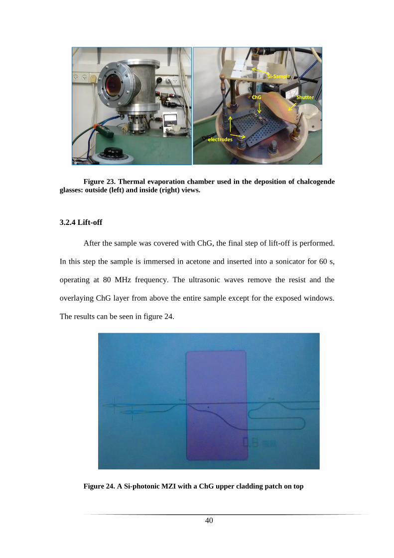
40
Figure 23. Thermal evaporation chamber used in the deposition of chalcogende
glasses: outside (left) and inside (right) views.
3.2.4 Lift-off
After the sample was covered with ChG, the final step of lift-off is performed.
In this step the sample is immersed in acetone and inserted into a sonicator for 60 s,
operating at 80 MHz frequency. The ultrasonic waves remove the resist and the
overlaying ChG layer from above the entire sample except for the exposed windows.
The results can be seen in figure 24.
Figure 24. A Si-photonic MZI with a ChG upper cladding patch on top
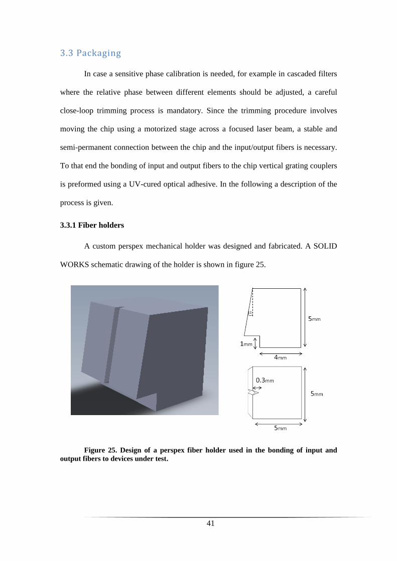
41
3.3 Packaging
In case a sensitive phase calibration is needed, for example in cascaded filters
where the relative phase between different elements should be adjusted, a careful
close-loop trimming process is mandatory. Since the trimming procedure involves
moving the chip using a motorized stage across a focused laser beam, a stable and
semi-permanent connection between the chip and the input/output fibers is necessary.
To that end the bonding of input and output fibers to the chip vertical grating couplers
is preformed using a UV-cured optical adhesive. In the following a description of the
process is given.
3.3.1 Fiber holders
A custom perspex mechanical holder was designed and fabricated. A SOLID
WORKS schematic drawing of the holder is shown in figure 25.
Figure 25. Design of a perspex fiber holder used in the bonding of input and
output fibers to devices under test.
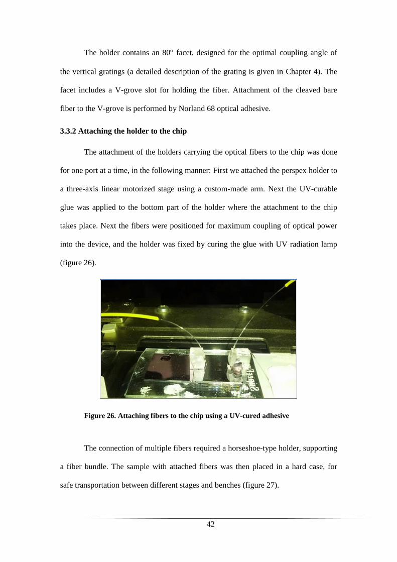
42
The holder contains an 80 facet, designed for the optimal coupling angle of
the vertical gratings (a detailed description of the grating is given in Chapter 4). The
facet includes a V-grove slot for holding the fiber. Attachment of the cleaved bare
fiber to the V-grove is performed by Norland 68 optical adhesive.
3.3.2 Attaching the holder to the chip
The attachment of the holders carrying the optical fibers to the chip was done
for one port at a time, in the following manner: First we attached the perspex holder to
a three-axis linear motorized stage using a custom-made arm. Next the UV-curable
glue was applied to the bottom part of the holder where the attachment to the chip
takes place. Next the fibers were positioned for maximum coupling of optical power
into the device, and the holder was fixed by curing the glue with UV radiation lamp
(figure 26).
Figure 26. Attaching fibers to the chip using a UV-cured adhesive
The connection of multiple fibers required a horseshoe-type holder, supporting
a fiber bundle. The sample with attached fibers was then placed in a hard case, for
safe transportation between different stages and benches (figure 27).
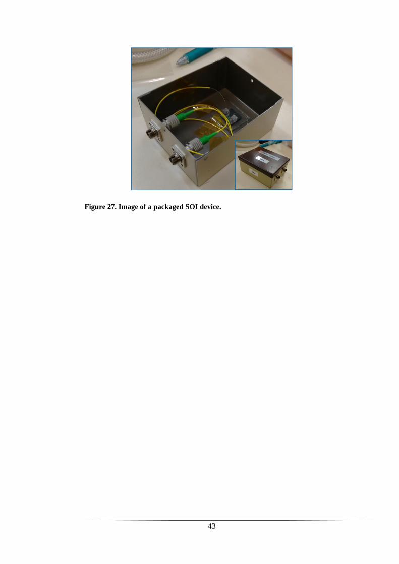
43
Figure 27. Image of a packaged SOI device.
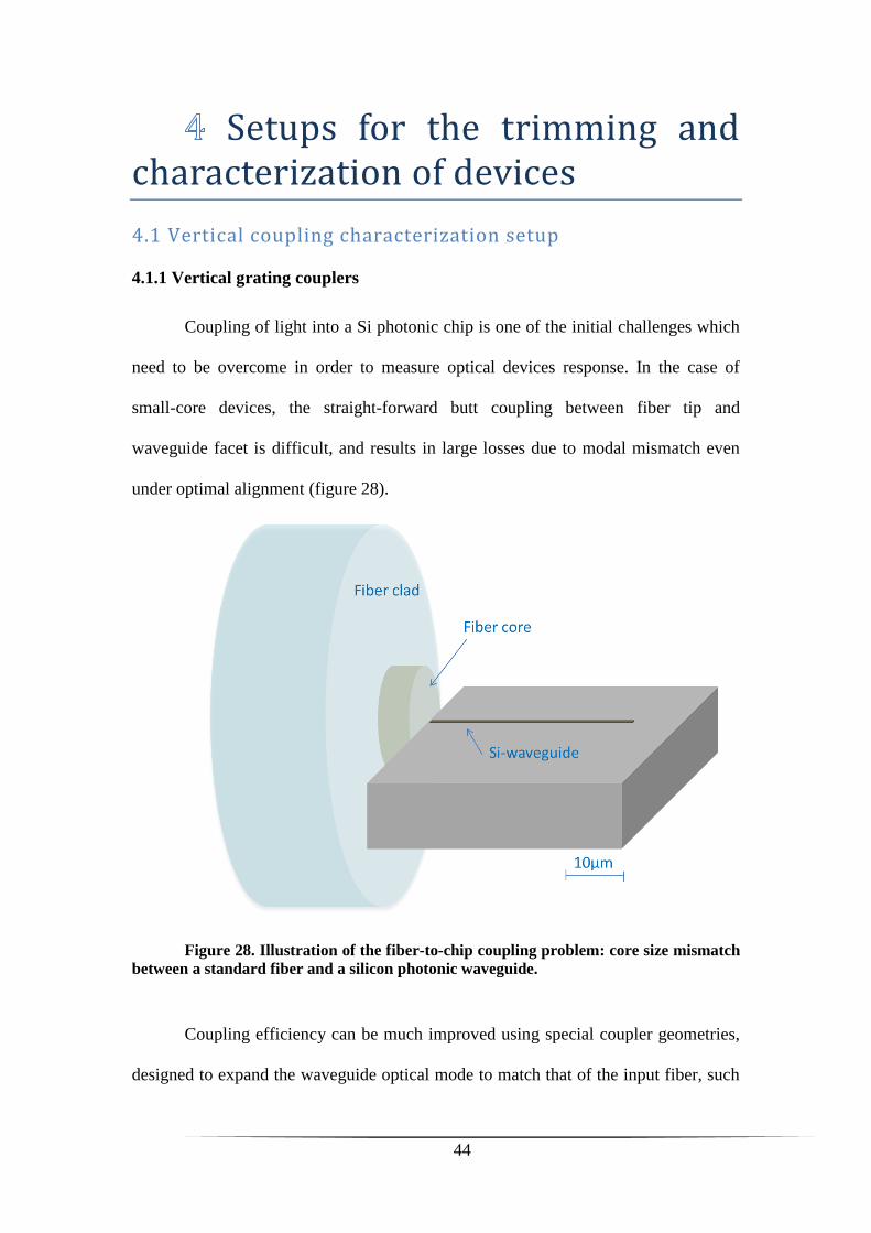
44
Setups for the trimming and characterization of devices
4.1 Vertical coupling characterization setup
4.1.1 Vertical grating couplers
Coupling of light into a Si photonic chip is one of the initial challenges which
need to be overcome in order to measure optical devices response. In the case of
small-core devices, the straight-forward butt coupling between fiber tip and
waveguide facet is difficult, and results in large losses due to modal mismatch even
under optimal alignment (figure 28).
Figure 28. Illustration of the fiber-to-chip coupling problem: core size mismatch
between a standard fiber and a silicon photonic waveguide.
Coupling efficiency can be much improved using special coupler geometries,
designed to expand the waveguide optical mode to match that of the input fiber, such
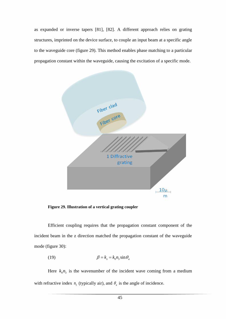
45
as expanded or inverse tapers [81], [82]. A different approach relies on grating
structures, imprinted on the device surface, to couple an input beam at a specific angle
to the waveguide core (figure 29). This method enables phase matching to a particular
propagation constant within the waveguide, causing the excitation of a specific mode.
Figure 29. Illustration of a vertical grating coupler
Efficient coupling requires that the propagation constant component of the
incident beam in the z direction matched the propagation constant of the waveguide
mode (figure 30):
(19) 0 3 sinz ak k n
Here 0 3k n is the wavenumber of the incident wave coming from a medium
with refractive index 3n (typically air), and a is the angle of incidence.
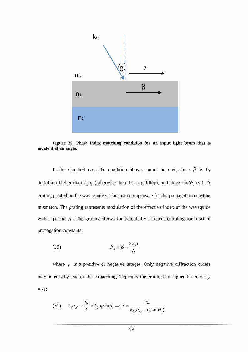
46
Figure 30. Phase index matching condition for an input light beam that is
incident at an angle.
In the standard case the condition above cannot be met, since is by
definition higher than 0 3k n (otherwise there is no guiding), and since sin( ) 1a . A
grating printed on the waveguide surface can compensate for the propagation constant
mismatch. The grating represents modulation of the effective index of the waveguide
with a period . The grating allows for potentially efficient coupling for a set of
propagation constants:
(20) 2
p
p
where p is a positive or negative integer. Only negative diffraction orders
may potentially lead to phase matching. Typically the grating is designed based on p
= -1:
(21) 0 0 3
0 3
2 2sin
( sin )eff a
eff a
k n k nk n n
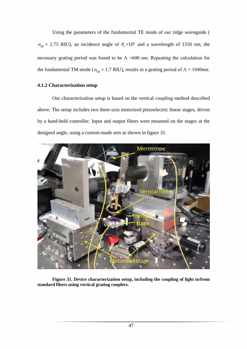
47
Using the parameters of the fundamental TE mode of our ridge waveguide (
effn = 2.75 RIU), an incidence angle of a =10 and a wavelength of 1550 nm, the
necessary grating period was found to be Λ =600 nm. Repeating the calculation for
the fundamental TM mode (effn = 1.7 RIU), results in a grating period of Λ = 1040nm.
4.1.2 Characterization setup
Our characterization setup is based on the vertical coupling method described
above. The setup includes two three-axis motorized piezoelectric linear stages, driven
by a hand-held controller. Input and output fibers were mounted on the stages at the
designed angle, using a custom-made arm as shown in figure 31.
Figure 31. Device characterization setup, including the coupling of light to/from
standard fibers using vertical grating couplers.
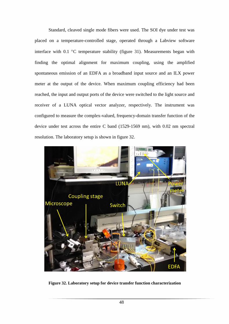
48
Standard, cleaved single mode fibers were used. The SOI dye under test was
placed on a temperature-controlled stage, operated through a Labview software
interface with 0.1 C temperature stability (figure 31). Measurements began with
finding the optimal alignment for maximum coupling, using the amplified
spontaneous emission of an EDFA as a broadband input source and an ILX power
meter at the output of the device. When maximum coupling efficiency had been
reached, the input and output ports of the device were switched to the light source and
receiver of a LUNA optical vector analyzer, respectively. The instrument was
configured to measure the complex-valued, frequency-domain transfer function of the
device under test across the entire C band (1529-1569 nm), with 0.02 nm spectral
resolution. The laboratory setup is shown in figure 32.
Figure 32. Laboratory setup for device transfer function characterization

49
4.2 Passive Si-photonic devices characterization
4.2.1 Si waveguide
As mentioned in the introduction, the photonic waveguide is the most basic
building block of any integrated circuit. Its characteristics directly affect the
performance of the entire integrated circuit, hence special care must be taken in the
design, fabrication and characterization process of the basic waveguide to obtain best
quality. We based our design primarily on ridge waveguides, partially etched to a
depth of 70 nm. Using this design, the guided optical mode is less exposed to
roughness at the sidewalls, resulting in considerably lower propagation losses. On the
other hand, ridge waveguides are more susceptible to bending losses.
Figure 33. Top-view SEM image of Si ridge waveguide (left), and a SEM image
of a FIB-processed cross section (right).
Figure 33 shows a scanning electron microscope (SEM) top-view image of a
BIU-made waveguide, alongside a focused ion beam (FIB)-processed cross section
showing basic structural dimensions. Figure 34 shows an atomic force microscope
(AFM) surface scan analysis for the same waveguide.

50
Figure 34. Atomic fornce microscope scanning profiles of a silicon-photonic
waveguide: Area scan (left) and line scan (right).
The coupling and propagation losses were characterized using a series of
waveguides with various lengths. End-to-end losses for each of the waveguides were
recorded. A graph showing the losses (in dB) vs. waveguide length (in mm) was
plotted (figure 35).
Figure 35. Measured end-to-end losses of silicon-photonic ridge waveguides of
different lengths.
51
A straight-line trend is observed in the results of figure 35, crossing the y axis
at the -16 dB point. This value represents an estimated coupling loss of 8 dB for each
vertical grating. The propagation losses per unit length are estimated based on the
slope of the graph, as -3.1 dB/cm. An alternative method for the evaluation of
waveguide propagation losses, based on the analysis of a ring resonator, is described
in section 4.2.3. While the propagation and coupling losses fall short of those obtained
in state-of-the-art facilities, or using specialized cross-sections [83], [84], they are
nevertheless respectable and sufficient for the proof of the concept of this research.
Sidewall roughness is a main contributor to waveguide losses, hence the smoothing of
the walls, using processes such as oxidation [85], may help improve losses
considerably.
4.2.2 Mach-Zehnder interferometers (MZIs)
The next elements to be tested were Mach-Zehender-Interferometer (MZI),
comprised of two directional couplers with imbalanced delays [5]. The power transfer
function of MZIs follows squared-cosine dependence, with periodic peaks and
notches (see in introduction), due to constructive and destructive interference between
the two paths. The extinction ratio between peaks and notches is determined by the
splitting ratios of the couplers and loss imbalance between paths. When both couplers
are balanced to 50%, and the MZI arms are sufficiently short so that differences
between propagation losses are negligible, the interference extinction ratio at both
outputs is ideally infinite. In the case of long differential delays of few mm or more,
unbalanced couplers might be required to compensate for the loss imbalance.

52
Figure 36. Measured power transfer function of a silicon-photonic MZI with
optimized 50% directional couplers
Finding the exact design for 50% power splitting is not straightforward, due to
fabrication tolerances in waveguides widths, etching depth, gap between cores etc. To
that end, a parameter sweep is often implemented in a series of devices. In our
experiments, using 700 nm-wide ridge waveguides with partial etch depth of 70 nm,
the optimal extinction ratio was obtained with directional couplers that were 14 µm-
long and had a 300 nm-wide gap separating the two cores. The power transfer
function of a device with a path length imbalance of 1 mm is presented in figure 36. A
FIB cross section of the coupler region is shown in figure 37.

53
Figure 37. A FIB cross-section of a directional coupler within a silicon-photonic
MZI device.
The FSR of the MZI was measured as 0.66 nm. The group delay index gn of
the waveguide may be calculated based on the FSR:
(22)
262
0
9 3
1.55 103.64
0.66 10 10g
MZI
nFSR l
RIU
Here l is the path length imbalance. This result agrees well with our
simulations of ridge waveguides (see Chapter 5).
4.2.3 Ring resonators
The third basic building block designed and fabricated at this stage is the ring
resonator. The resonators can be designed in few geometrical layouts, where the most
popular are the circular and the race-track geometries. Attention must be given to the
minimal bending radius within the ring, and to the coupling between the ring and bus
waveguide. The gap between bus and ring resonator varies with position, whereas the
gap between the bus and a race-track layout is fixed. Maximum extinction ratio is
achieved at the condition of critical coupling (see Chapter 1, [5]), in which the
coupling of light into the ring compensates perfectly for the round-trip propagation

54
losses. Here too, calibrations were made using a parameter sweep of the coupler
geometry. Figure 38 shows the measured transfer function of a critically-coupled 125
μm circumference resonator .A SEM image of the fabricated device is shown in figure
39.
Figure 38. Measured power transfer function of a ring resonator with 125 µm
circumference
Figure 39. Top-view SEM image of Si ring resonator
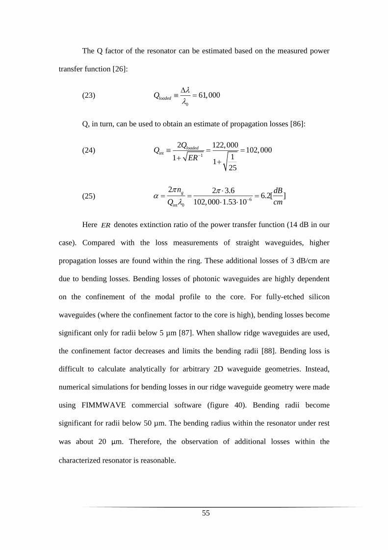
55
The Q factor of the resonator can be estimated based on the measured power
transfer function [26]:
(23) 0
61,000loadedQ
Q, in turn, can be used to obtain an estimate of propagation losses [86]:
(24) int1
2 122,000102,000
111
25
loadedQQ
ER
(25) 6
int 0
2 2 3.66.2[ ]
102,000 1.53 10
gn dB
Q cm
Here ER denotes extinction ratio of the power transfer function (14 dB in our
case). Compared with the loss measurements of straight waveguides, higher
propagation losses are found within the ring. These additional losses of 3 dB/cm are
due to bending losses. Bending losses of photonic waveguides are highly dependent
on the confinement of the modal profile to the core. For fully-etched silicon
waveguides (where the confinement factor to the core is high), bending losses become
significant only for radii below 5 µm [87]. When shallow ridge waveguides are used,
the confinement factor decreases and limits the bending radii [88]. Bending loss is
difficult to calculate analytically for arbitrary 2D waveguide geometries. Instead,
numerical simulations for bending losses in our ridge waveguide geometry were made
using FIMMWAVE commercial software (figure 40). Bending radii become
significant for radii below 50 µm. The bending radius within the resonator under rest
was about 20 µm. Therefore, the observation of additional losses within the
characterized resonator is reasonable.
56
Figure 40. Numercial simulations of bending losses in an SOI ridge waveguide,
calculated using FIMMWAVE commercial software.
4.3 Mass-transfer trimming setup
Response trimming based on selective photo-induced mass transfer of
As10Se90 layers was carried out using a 532 nm laser source. The absorption of
incident light at this wavelength, in this particular composition, was evaluated from
spectroscopy measurements, seen in figure 41 below.
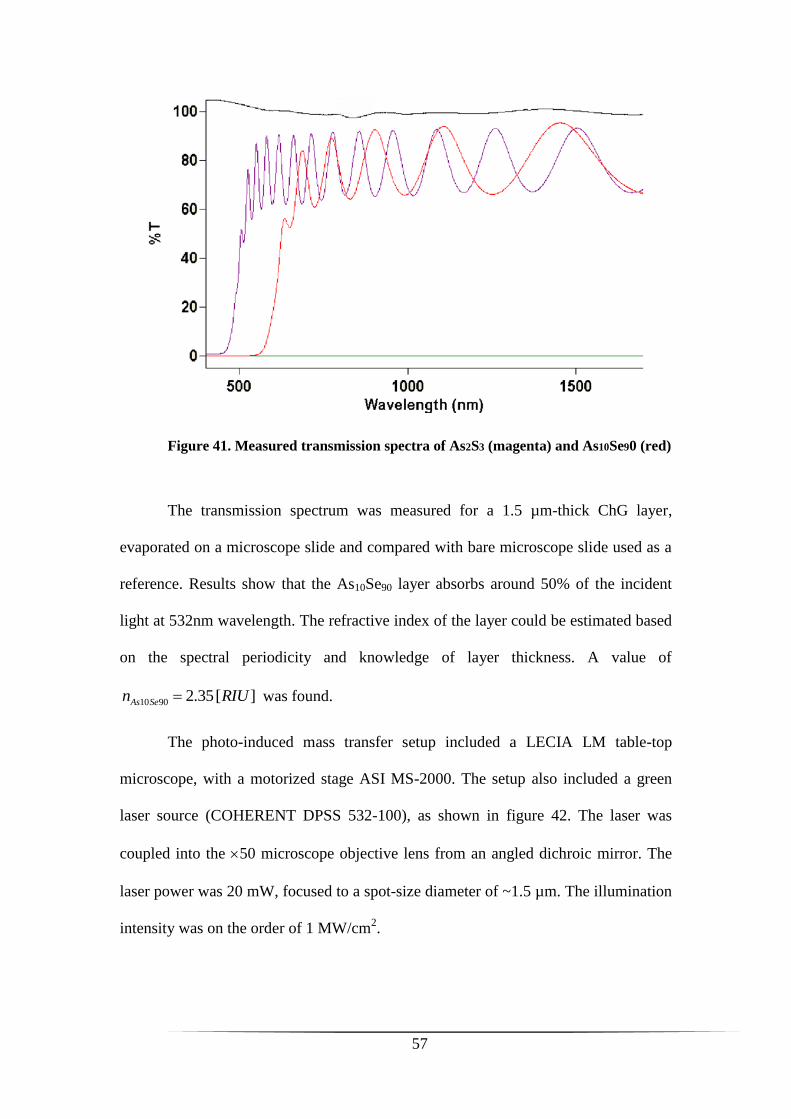
57
Figure 41. Measured transmission spectra of As2S3 (magenta) and As10Se90 (red)
The transmission spectrum was measured for a 1.5 µm-thick ChG layer,
evaporated on a microscope slide and compared with bare microscope slide used as a
reference. Results show that the As10Se90 layer absorbs around 50% of the incident
light at 532nm wavelength. The refractive index of the layer could be estimated based
on the spectral periodicity and knowledge of layer thickness. A value of
10 90 2.35[ ]As Sen RIU was found.
The photo-induced mass transfer setup included a LECIA LM table-top
microscope, with a motorized stage ASI MS-2000. The setup also included a green
laser source (COHERENT DPSS 532-100), as shown in figure 42. The laser was
coupled into the 50 microscope objective lens from an angled dichroic mirror. The
laser power was 20 mW, focused to a spot-size diameter of ~1.5 µm. The illumination
intensity was on the order of 1 MW/cm2.
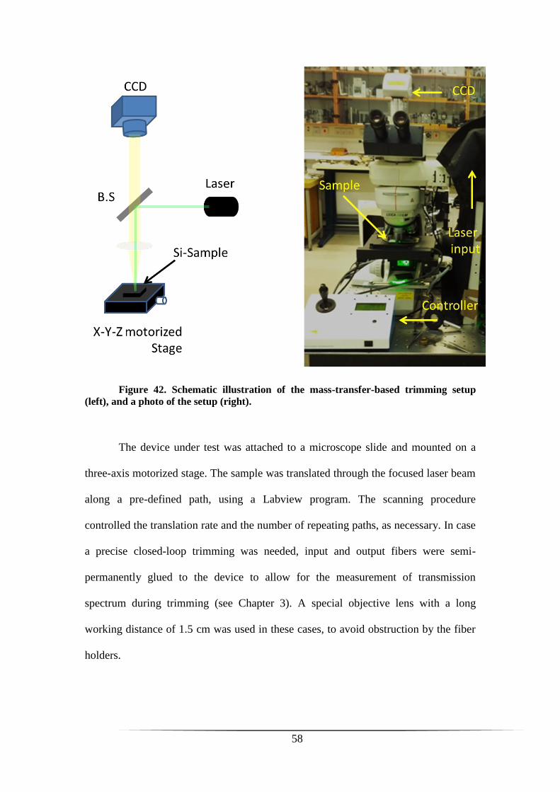
58
Figure 42. Schematic illustration of the mass-transfer-based trimming setup
(left), and a photo of the setup (right).
The device under test was attached to a microscope slide and mounted on a
three-axis motorized stage. The sample was translated through the focused laser beam
along a pre-defined path, using a Labview program. The scanning procedure
controlled the translation rate and the number of repeating paths, as necessary. In case
a precise closed-loop trimming was needed, input and output fibers were semi-
permanently glued to the device to allow for the measurement of transmission
spectrum during trimming (see Chapter 3). A special objective lens with a long
working distance of 1.5 cm was used in these cases, to avoid obstruction by the fiber
holders.
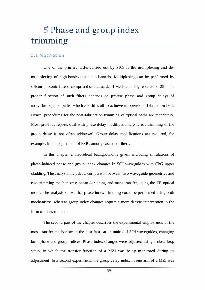
59
Phase and group index trimming
5.1 Motivation
One of the primary tasks carried out by PICs is the multiplexing and de-
multiplexing of high-bandwidth data channels. Multiplexing can be performed by
silicon-photonic filters, comprised of a cascade of MZIs and ring resonators [25]. The
proper function of such filters depends on precise phase and group delays of
individual optical paths, which are difficult to achieve in open-loop fabrication [91].
Hence, procedures for the post-fabrication trimming of optical paths are mandatory.
Most previous reports deal with phase delay modifications, whereas trimming of the
group delay is not often addressed. Group delay modifications are required, for
example, in the adjustment of FSRs among cascaded filters.
In this chapter a theoretical background is given, including simulations of
photo-induced phase and group index changes in SOI waveguides with ChG upper
cladding. The analysis includes a comparison between two waveguide geometries and
two trimming mechanisms: photo-darkening and mass-transfer, using the TE optical
mode. The analysis shows that phase index trimming could be performed using both
mechanisms, whereas group index changes require a more drastic intervention in the
form of mass-transfer.
The second part of the chapter describes the experimental employment of the
mass transfer mechanism in the post-fabrication tuning of SOI waveguides, changing
both phase and group indices. Phase index changes were adjusted using a close-loop
setup, in which the transfer function of a MZI was being monitored during its
adjustment. In a second experiment, the group delay index in one arm of a MZI was

60
modified by 0.07 RIU, through selective photo-removal of the upper cladding. The
FSR of the MZI was modified by 1%. The duration of the trimming process was only
a few seconds.
5.2 Phase trimming principles and simulations
5.2.1 Phase trimming based on the photo-darkening mechanism
Trimming of SOI waveguides can be achieved through local photo-darkening
of an upper ChG cladding layer. The laboratory setup used in the photo-darkening
experiment (Chapter 4) consists on a femtosecond pulse laser with a central
wavelength of 810 nm (E=1.53eV). As2S3 is transparent in that wavelength (bandgap
of 2.4 eV), hence index modifications are induced by a two-photon process. The
written change to the refractive index is permanent, and can be erased only by
annealing: the exposure of the sample to 420 K temperature for few hours [76]. The
extent of refractive index change increases with illumination intensity (figure 43).
Index variations saturate at about 0.08 RIU, for average intensities above 0.25
GW/cm2.
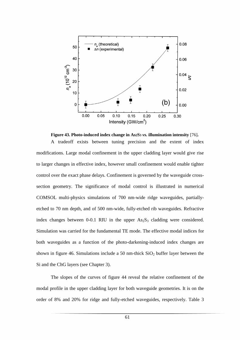
61
Figure 43. Photo-induced index change in As2S3 vs. illumination intensity [76].
A tradeoff exists between tuning precision and the extent of index
modifications. Large modal confinement in the upper cladding layer would give rise
to larger changes in effective index, however small confinement would enable tighter
control over the exact phase delays. Confinement is governed by the waveguide cross-
section geometry. The significance of modal control is illustrated in numerical
COMSOL multi-physics simulations of 700 nm-wide ridge waveguides, partially-
etched to 70 nm depth, and of 500 nm-wide, fully-etched rib waveguides. Refractive
index changes between 0-0.1 RIU in the upper As2S3 cladding were considered.
Simulation was carried for the fundamental TE mode. The effective modal indices for
both waveguides as a function of the photo-darkening-induced index changes are
shown in figure 46. Simulations include a 50 nm-thick SiO2 buffer layer between the
Si and the ChG layers (see Chapter 3).
The slopes of the curves of figure 44 reveal the relative confinement of the
modal profile in the upper cladding layer for both waveguide geometries. It is on the
order of 8% and 20% for ridge and fully-etched waveguides, respectively. Table 3

62
summarized the effective index changes for maximum refractive index change (0.1
RIU) in the upper As2S3 layer, for the two geometries. Larger variations are
anticipated for the fully-etched geometry, due to the larger confinement in the upper
cladding. Simulations are in general agreement with previous results [42], in which an
effective index modification of 0.016 RIU was reported using a 450 nm-wide fully
etched waveguide.
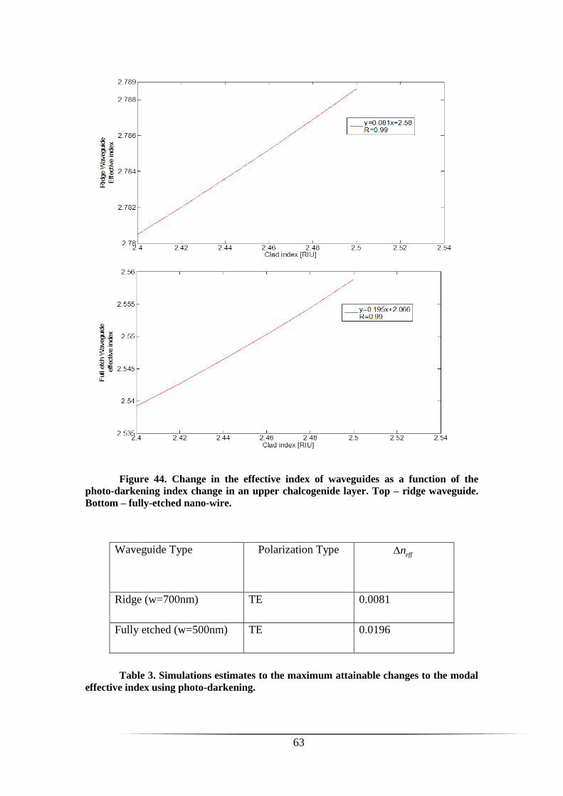
63
Figure 44. Change in the effective index of waveguides as a function of the
photo-darkening index change in an upper chalcogenide layer. Top – ridge waveguide.
Bottom – fully-etched nano-wire.
Waveguide Type Polarization Type effn
Ridge (w=700nm) TE 0.0081
Fully etched (w=500nm) TE 0.0196
Table 3. Simulations estimates to the maximum attainable changes to the modal
effective index using photo-darkening.

64
As discussed in Chapter 3, a buffer layer of silica is used between the silicon
waveguide core and the upper cladding layer. Figure 45 shows the simulated change
in effective index of a fully-etched waveguide as a function of the buffer layer
thickness. Photo-darkening of the upper layer by 0.1 RIU is assumed. The extent of
effective index tuning decreases exponentially with the buffer layer thickness. The
expected index change using a 50 nm-thick layer is about half of that anticipated with
no buffer at all. The buffer layer is required, however, to mitigate losses at the
interface.
Figure 45. Calculated changes to the effective index of a fully-etched waveguide
as a function of the thickness of a silica buffer layer. Photo-induced change to the index
of the upper cladding layer by 0.1 RIU is assumed.
5.2.2 Phase trimming based on mass-transfer mechanism
Mass transfer was employed in the photo-removal of an upper cladding layer
of As10Se90. The lack of As in the glass matrix weakens the atomic bonds and lowers
65
the temperature of glass transition. The absorption of light above bandgap elevates the
local temperature above the Tg value, leading to lateral flow of the glass from hot to
cold regions [92]. The effect is used to selectively remove the upper cladding from
above sections of the silicon waveguide core. This change in the geometry brings
about rather drastic changes to the phase and group indices of the guided mode.
Figure 46 shows numerical simulation results of the modal effective index as a
function of the upper ChG cladding thickness. The simulation was carried for the TE
mode and addresses the two waveguide geometries of the previous section.
Figure 46. Waveguide effective index change vs. residual thickness of an upper
cladding layer: Ridge waveguide (top), and fully etched waveguide (bottom)
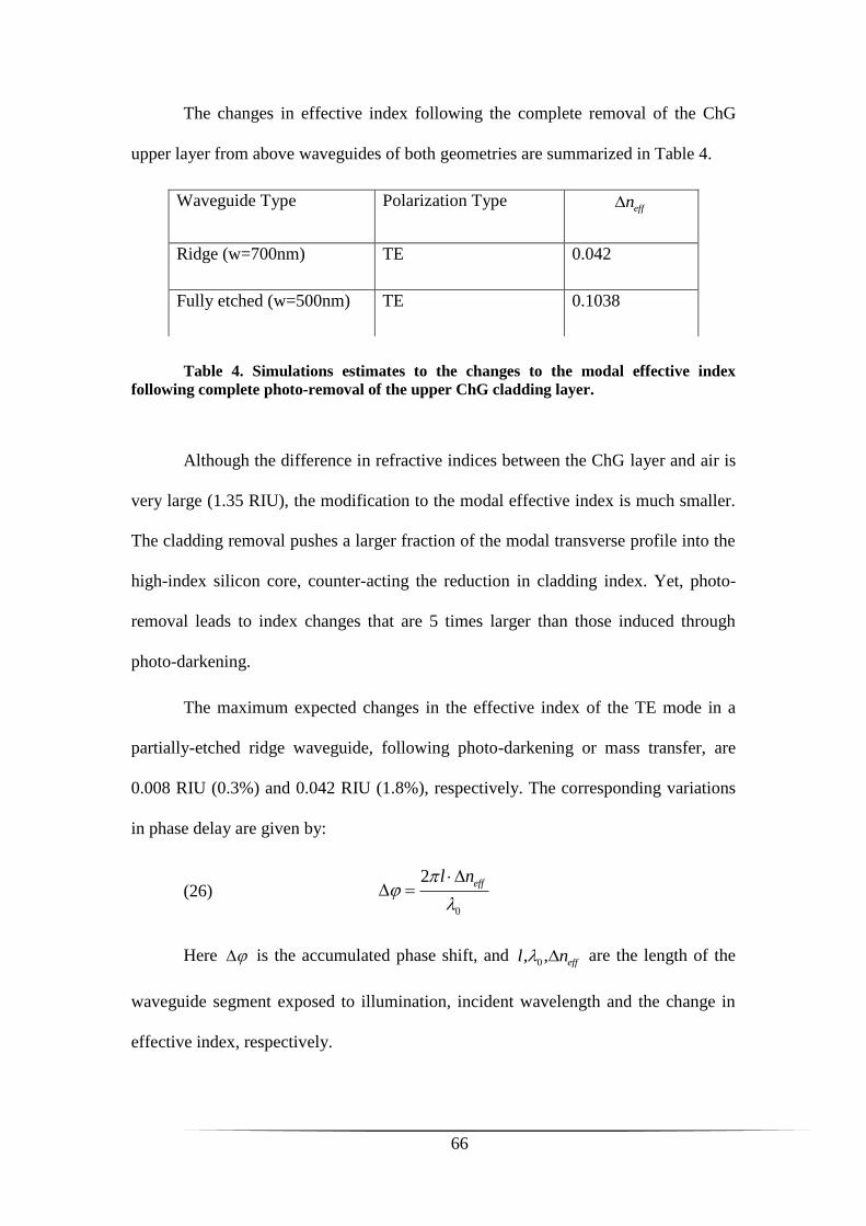
66
The changes in effective index following the complete removal of the ChG
upper layer from above waveguides of both geometries are summarized in Table 4.
Table 4. Simulations estimates to the changes to the modal effective index
following complete photo-removal of the upper ChG cladding layer.
Although the difference in refractive indices between the ChG layer and air is
very large (1.35 RIU), the modification to the modal effective index is much smaller.
The cladding removal pushes a larger fraction of the modal transverse profile into the
high-index silicon core, counter-acting the reduction in cladding index. Yet, photo-
removal leads to index changes that are 5 times larger than those induced through
photo-darkening.
The maximum expected changes in the effective index of the TE mode in a
partially-etched ridge waveguide, following photo-darkening or mass transfer, are
0.008 RIU (0.3%) and 0.042 RIU (1.8%), respectively. The corresponding variations
in phase delay are given by:
(26) 0
2 effl n
Here is the accumulated phase shift, and 0, , effl n are the length of the
waveguide segment exposed to illumination, incident wavelength and the change in
effective index, respectively.
Waveguide Type Polarization Type effn
Ridge (w=700nm) TE 0.042
Fully etched (w=500nm) TE 0.1038

67
The dependence of the index change on the thickness of the silica buffer layer,
following complete removal of the upper cladding, is shown in figure 47. Exponential
decrease in index modification is anticipated in this case as well.
Figure 47. Calculated changes to the effective index of a fully-etched waveguide
as a function of the thickness of a silica buffer layer, following the complete photo-
removal of the upper cladding layer.
5.3 Group index trimming theory and simulations
5.3.1 Theory and simulations
The group delay index of an optical medium is defined by the following
expression [5]:
(27) 0
eff
g eff
nn n
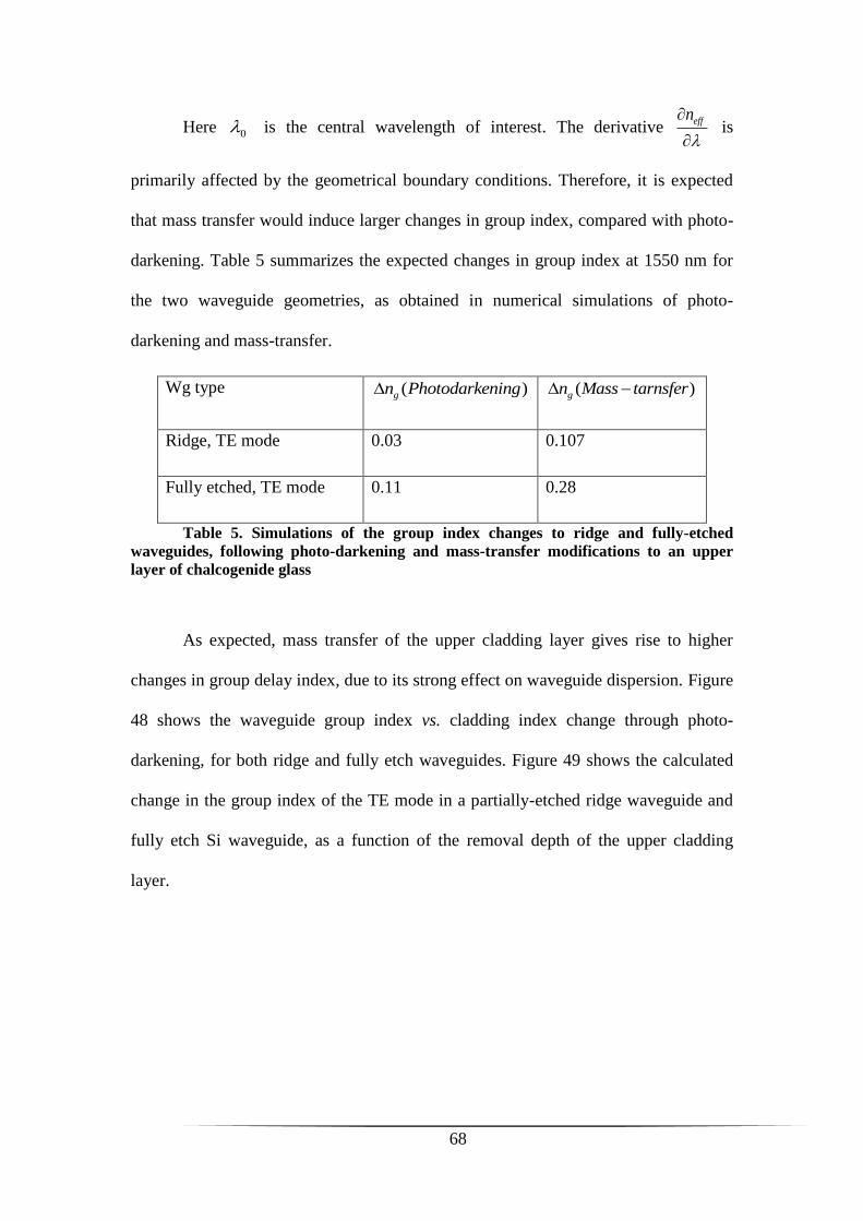
68
Here 0 is the central wavelength of interest. The derivative effn
is
primarily affected by the geometrical boundary conditions. Therefore, it is expected
that mass transfer would induce larger changes in group index, compared with photo-
darkening. Table 5 summarizes the expected changes in group index at 1550 nm for
the two waveguide geometries, as obtained in numerical simulations of photo-
darkening and mass-transfer.
As expected, mass transfer of the upper cladding layer gives rise to higher
changes in group delay index, due to its strong effect on waveguide dispersion. Figure
48 shows the waveguide group index vs. cladding index change through photo-
darkening, for both ridge and fully etch waveguides. Figure 49 shows the calculated
change in the group index of the TE mode in a partially-etched ridge waveguide and
fully etch Si waveguide, as a function of the removal depth of the upper cladding
layer.
Wg type ( )gn Photodarkening ( )gn Mass tarnsfer
Ridge, TE mode 0.03 0.107
Fully etched, TE mode 0.11 0.28
Table 5. Simulations of the group index changes to ridge and fully-etched
waveguides, following photo-darkening and mass-transfer modifications to an upper
layer of chalcogenide glass

69
Figure 48.Group delay index vs. the refractive index of an upper cladding layer,
for a fully-etched waveguide (top) and a ridge waveguide (bottom).

70
Figure 49.Group delay index vs. the residual thickness of an upper cladding
layer, for ridge waveguide (top) and fully etched waveguide (bottom)
5.4 Experimental results
5.4.1 Phase trimming
To demonstrate the phase trimming effect, MZIs with a path imbalance of 1
mm were fabricated in SOI according to the process described in Chapter 3. A 100 x
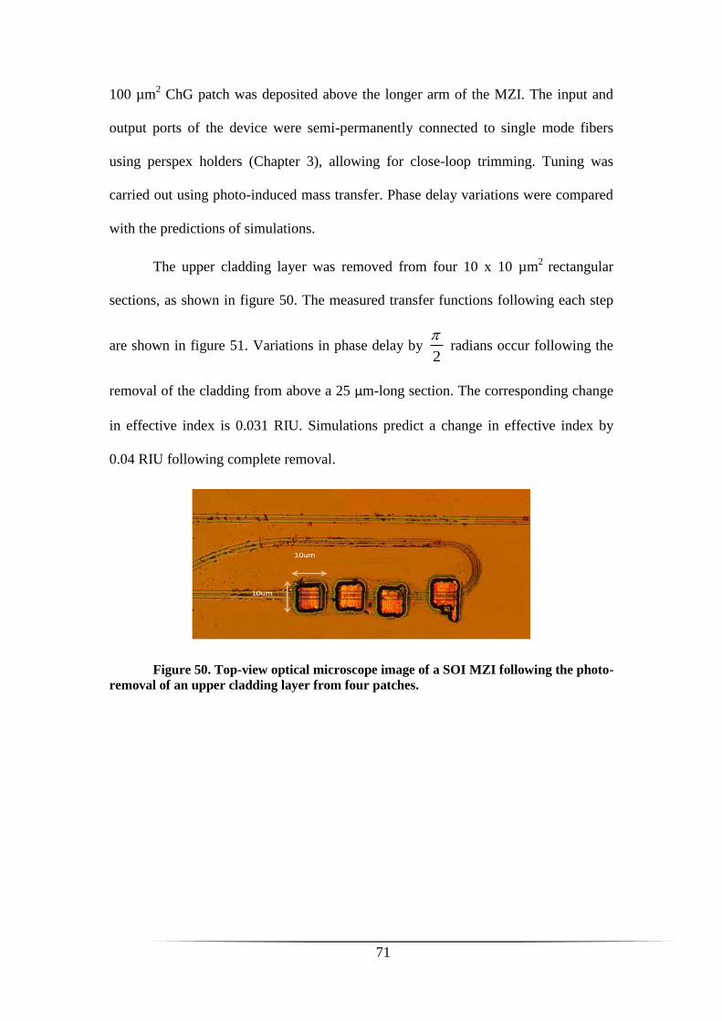
71
100 µm2 ChG patch was deposited above the longer arm of the MZI. The input and
output ports of the device were semi-permanently connected to single mode fibers
using perspex holders (Chapter 3), allowing for close-loop trimming. Tuning was
carried out using photo-induced mass transfer. Phase delay variations were compared
with the predictions of simulations.
The upper cladding layer was removed from four 10 x 10 µm2
rectangular
sections, as shown in figure 50. The measured transfer functions following each step
are shown in figure 51. Variations in phase delay by 2
radians occur following the
removal of the cladding from above a 25 µm-long section. The corresponding change
in effective index is 0.031 RIU. Simulations predict a change in effective index by
0.04 RIU following complete removal.
Figure 50. Top-view optical microscope image of a SOI MZI following the photo-
removal of an upper cladding layer from four patches.
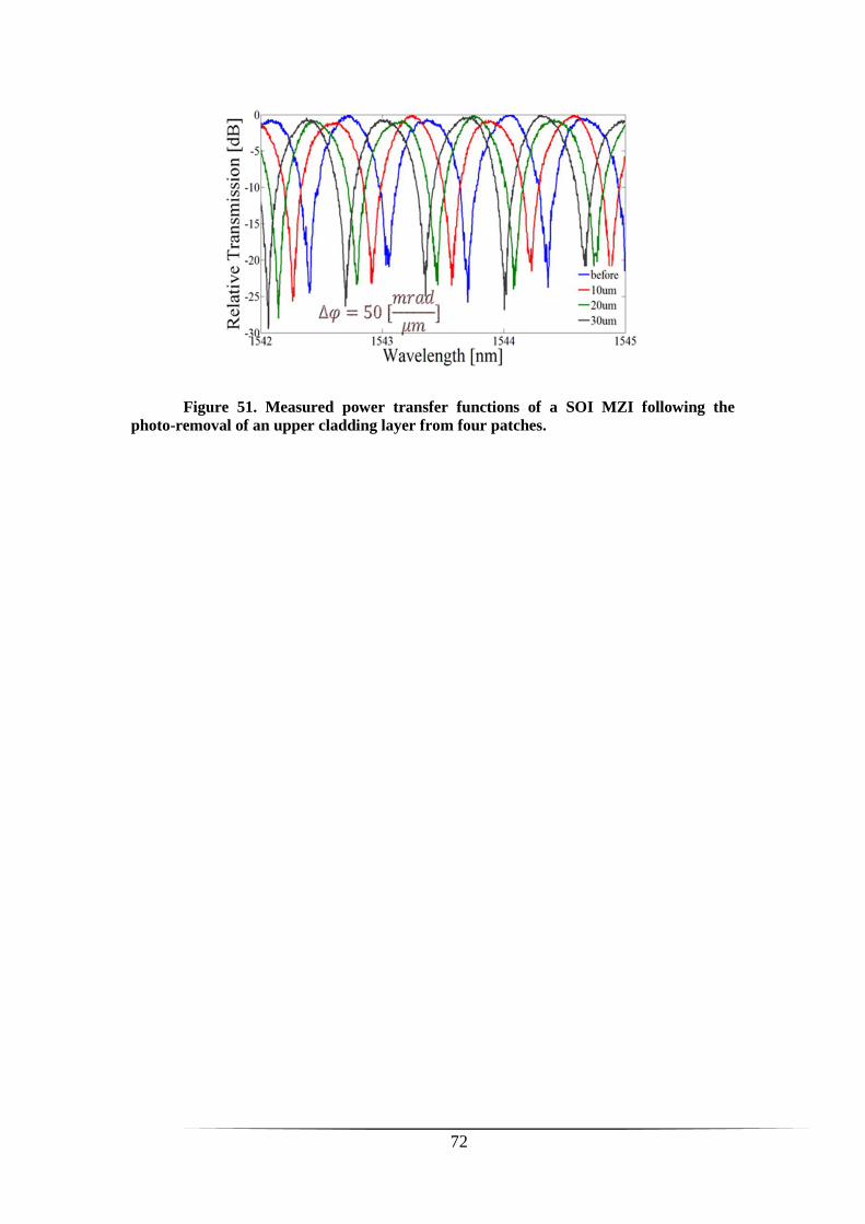
72
Figure 51. Measured power transfer functions of a SOI MZI following the
photo-removal of an upper cladding layer from four patches.
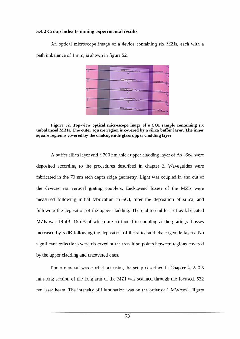
73
5.4.2 Group index trimming experimental results
An optical microscope image of a device containing six MZIs, each with a
path imbalance of 1 mm, is shown in figure 52.
Figure 52. Top-view optical microscope inage of a SOI sample containing six
unbalanced MZIs. The outer square region is covered by a silica buffer layer. The inner
square region is covered by the chalcogenide glass upper cladding layer
A buffer silica layer and a 700 nm-thick upper cladding layer of As10Se90 were
deposited according to the procedures described in chapter 3. Waveguides were
fabricated in the 70 nm etch depth ridge geometry. Light was coupled in and out of
the devices via vertical grating couplers. End-to-end losses of the MZIs were
measured following initial fabrication in SOI, after the deposition of silica, and
following the deposition of the upper cladding. The end-to-end loss of as-fabricated
MZIs was 19 dB, 16 dB of which are attributed to coupling at the gratings. Losses
increased by 5 dB following the deposition of the silica and chalcogenide layers. No
significant reflections were observed at the transition points between regions covered
by the upper cladding and uncovered ones.
Photo-removal was carried out using the setup described in Chapter 4. A 0.5
mm-long section of the long arm of the MZI was scanned through the focused, 532
nm laser beam. The intensity of illumination was on the order of 1 MW/cm2. Figure

74
53 shows a top-view optical microscope image of the MZI following photo-removal,
and an atomic force microscope (AFM) scanning of part of the illuminated region.
Figure 53. Top – Optical microscope top-view image of a MZI with 1 mm path
imbalance, following the photo-removal of the upper cladding layer from a above a 0.5
mm-long segment of the silicon core in the longer arm. Center – AFM scan of part of the
region in which
Figure 54 shows a scanning electron microscope (SEM) image of a cross-
section of the waveguide following photo-removal, formed by a FIB. Only 50 nm of
the original 700 nm-thick upper cladding layer remain above the waveguide core.
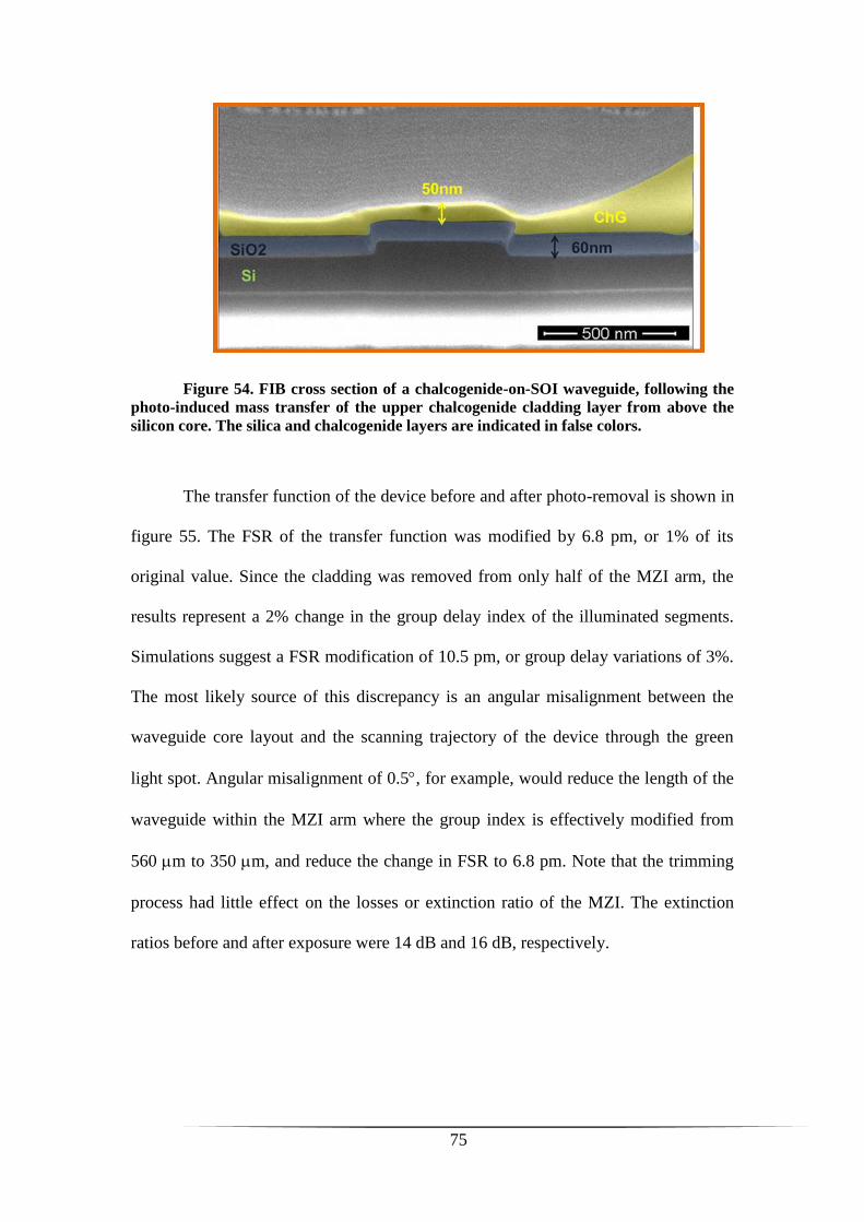
75
Figure 54. FIB cross section of a chalcogenide-on-SOI waveguide, following the
photo-induced mass transfer of the upper chalcogenide cladding layer from above the
silicon core. The silica and chalcogenide layers are indicated in false colors.
The transfer function of the device before and after photo-removal is shown in
figure 55. The FSR of the transfer function was modified by 6.8 pm, or 1% of its
original value. Since the cladding was removed from only half of the MZI arm, the
results represent a 2% change in the group delay index of the illuminated segments.
Simulations suggest a FSR modification of 10.5 pm, or group delay variations of 3%.
The most likely source of this discrepancy is an angular misalignment between the
waveguide core layout and the scanning trajectory of the device through the green
light spot. Angular misalignment of 0.5, for example, would reduce the length of the
waveguide within the MZI arm where the group index is effectively modified from
560 m to 350 m, and reduce the change in FSR to 6.8 pm. Note that the trimming
process had little effect on the losses or extinction ratio of the MZI. The extinction
ratios before and after exposure were 14 dB and 16 dB, respectively.
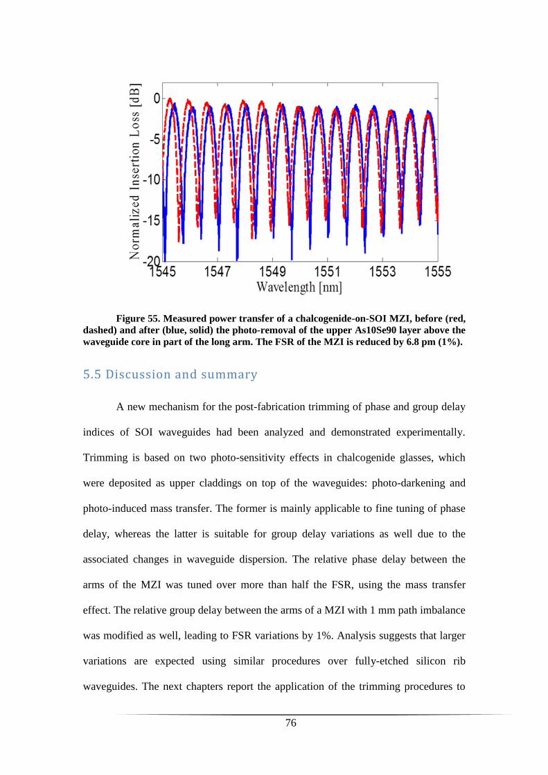
76
Figure 55. Measured power transfer of a chalcogenide-on-SOI MZI, before (red,
dashed) and after (blue, solid) the photo-removal of the upper As10Se90 layer above the
waveguide core in part of the long arm. The FSR of the MZI is reduced by 6.8 pm (1%).
5.5 Discussion and summary
A new mechanism for the post-fabrication trimming of phase and group delay
indices of SOI waveguides had been analyzed and demonstrated experimentally.
Trimming is based on two photo-sensitivity effects in chalcogenide glasses, which
were deposited as upper claddings on top of the waveguides: photo-darkening and
photo-induced mass transfer. The former is mainly applicable to fine tuning of phase
delay, whereas the latter is suitable for group delay variations as well due to the
associated changes in waveguide dispersion. The relative phase delay between the
arms of the MZI was tuned over more than half the FSR, using the mass transfer
effect. The relative group delay between the arms of a MZI with 1 mm path imbalance
was modified as well, leading to FSR variations by 1%. Analysis suggests that larger
variations are expected using similar procedures over fully-etched silicon rib
waveguides. The next chapters report the application of the trimming procedures to

77
the alignment of the transfer functions of cascaded MZI stages, and to adjustments of
the power splitting ratio in directional couplers.
78
Directional coupler trimming
6.1 Motivation
Directional couplers are among the most fundamental building blocks of
integrated photonics filters. They are used to combine or split incoming light between
waveguide paths, cascaded to form MZIs, and linked to provide feedback in ring
resonators [25]. The performance metrics of filters depend critically on precise
coupling ratios which may vary due to inevitable fabrication tolerances [91]. Tunable
couplers can be implemented, for example, by balanced MZIs with adjustable
differential phases [25]. A wavelength-independent, arbitrary coupling ratio can be
obtained, at the expense of increased footprint and complexity [25]. If possible, the
post-fabrication tuning of a single directional coupler, over a broad range of coupling
ratios, would represent a useful alternative.
Active tuning of photonic devices relies on localized heating [33], [93], [94],
injection of free carriers into p-i-n junction structures [34], [95], or use of liquid
crystals [96]. Several of these methods were also employed in the active tuning of
couplers [96], [97]. Active tuning approaches, however, increase the complexity of
passive devices and require constant feedback. While many approaches had been
proposed for the one-time trimming of phase delays [35], [36], [38], [40], [42], [98–
100], comparatively few works addressed the one-time adjustment of directional
couplers. In one notable example, the splitting ratio of polymer waveguide Y-
junctions was modified by photo-bleaching [101].
In this chapter, I show that the coupling ratio of SOI directional couplers may
be modified by the selective photo-removal of the upper cladding layer from above

79
part of their lengths. Numerical analysis suggests that the coupling coefficient per unit
length between the TE modes of two parallel, partially-etched ridge waveguides can
be modified by over 10%. Changes in the coupling coefficient between TE modes of
fully-etched waveguides reach 45%. The power coupling ratio of a 50 μm-long
directional coupler comprised of two such waveguides may be tuned continuously
between 0 and 1, with comparatively weak wavelength dependence. The response and
dimensions of these couplers are compatible with practical device requirements.
The method is demonstrated experimentally in the post-fabrication tuning of
SOI racetrack resonators: the extinction ratios of resonances at specific wavelength
ranges are continuously adjusted between 4 and 40 dB. The measured transfer
functions following several photo-removal steps are in good agreement with the
predictions of simulations. The coupling ratios of tuned devices changed little
following three months of storage.
6.2 Theory and simulation
We consider first a directional coupler between a pair of 700 nm-wide,
partially etched SOI ridge waveguides. The thickness of the silicon device layer is 220
nm, and it is etched to a residual thickness of 150 nm outside core regions. The lateral
gap between the cores is 300 nm-wide. The thickness of the buried oxide layer of the
SOI substrate is 2 μm. The cores are covered by a 50 nm-thick silica buffer layer,
followed by a 700 nm-thick upper cladding layer of As10Se90.
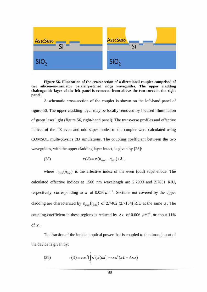
80
Figure 56. Illustration of the cross-section of a directional coupler comprised of
two silicon-on-insulator partially-etched ridge waveguides. The upper cladding
chalcogenide layer of the left panel is removed from above the two cores in the right
panel.
A schematic cross-section of the coupler is shown on the left-hand panel of
figure 56. The upper cladding layer may be locally removed by focused illumination
of green laser light (figure 56, right-hand panel). The transverse profiles and effective
indices of the TE even and odd super-modes of the coupler were calculated using
COMSOL multi-physics 2D simulations. The coupling coefficient between the two
waveguides, with the upper cladding layer intact, is given by [23]:
(28) ( ) ( ) /even oddn n ,
where ( )even oddn n is the effective index of the even (odd) super-mode. The
calculated effective indices at 1560 nm wavelength are 2.7909 and 2.7631 RIU,
respectively, corresponding to of 0.0561m . Sections not covered by the upper
cladding are characterized by ( )even oddn n of 2.7402 (2.7154) RIU at the same . The
coupling coefficient in these regions is reduced by of 0.006 1m , or about 11%
of .
The fraction of the incident optical power that is coupled to the through port of
the device is given by:
(29) 2 ' ' ' 2
0
( ) cos [ ( ) ] cos ( )
L
r x dx L x

81
Here L is the overall length of the coupler, and x is the length of the segment
that is not covered by the upper cladding. The position-dependent coupling coefficient
′in Eq. (26) equals for 0 ' ( )x L x , and for ( ) 'L x x L . Figure
57 shows the calculated ( )r between ridge waveguides of the geometry described
above, over a length of 300 μm and for different values of x . The simulations take
into consideration the chromatic dispersion of evenn and oddn .
Figure 57. Calculated power coupling ratios of a 300 µm-long directional
coupler, formed between two partially-etched, 700 nm-wide silicon-photonic ridge
waveguides. The transverse separation between the waveguides cores is 300 nm.
Different curves correspond to d
The simulation results suggest that ( )r may be tuned over a comparatively
broad range of values, between 0.4 and 1 at 1560 nm, through changing x . The long
coupler is, however, strongly wavelength-dependent. Larger relative changes in
coupling coefficient can be achieved using fully-etched silicon rib waveguides. We
considered typical waveguides of 500 nm width and 220 nm height, separated by a
200 nm-wide transverse gap between their cores and covered by a silica buffer layer
and an upper cladding of As10Se90 as detailed earlier. The calculated value of
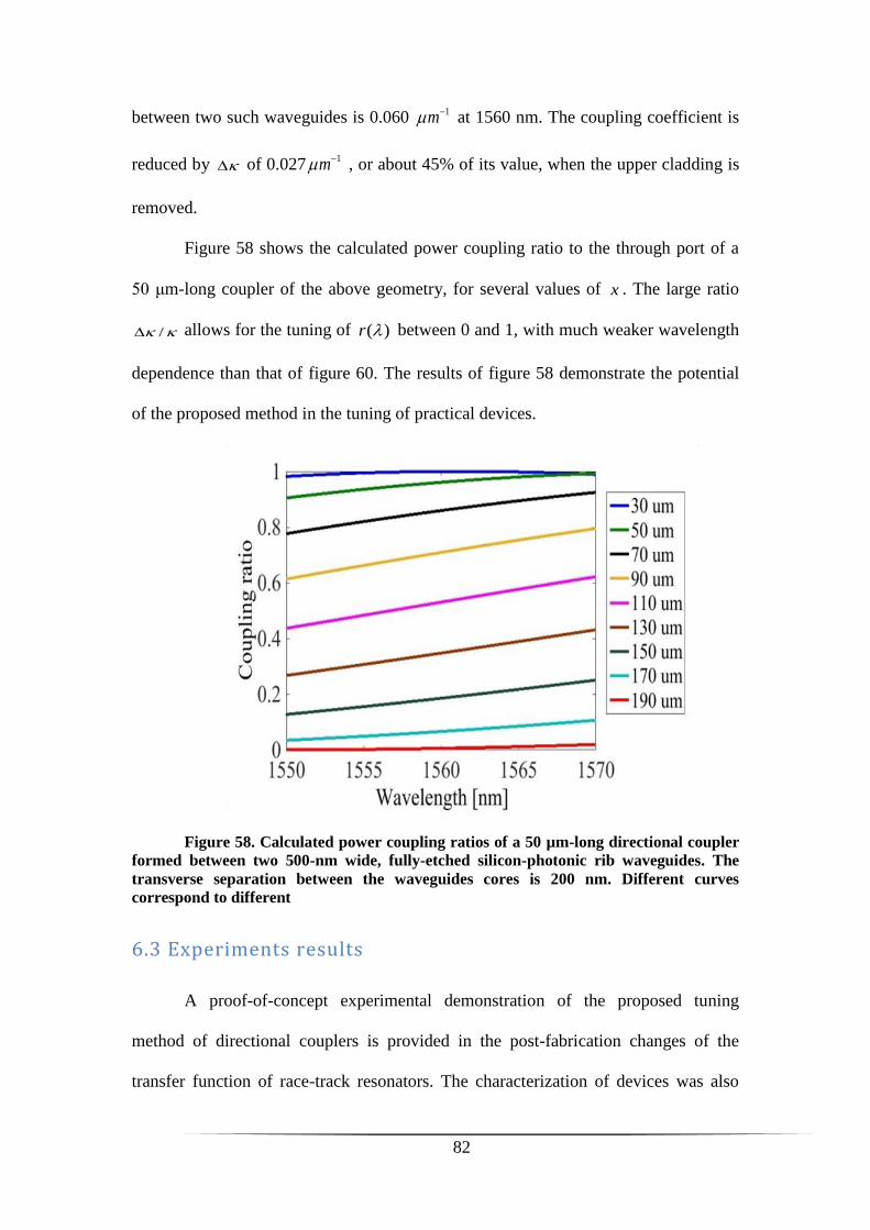
82
between two such waveguides is 0.060 1m at 1560 nm. The coupling coefficient is
reduced by of 0.0271m , or about 45% of its value, when the upper cladding is
removed.
Figure 58 shows the calculated power coupling ratio to the through port of a
50 μm-long coupler of the above geometry, for several values of x . The large ratio
/ allows for the tuning of ( )r between 0 and 1, with much weaker wavelength
dependence than that of figure 60. The results of figure 58 demonstrate the potential
of the proposed method in the tuning of practical devices.
Figure 58. Calculated power coupling ratios of a 50 µm-long directional coupler
formed between two 500-nm wide, fully-etched silicon-photonic rib waveguides. The
transverse separation between the waveguides cores is 200 nm. Different curves
correspond to different
6.3 Experiments results
A proof-of-concept experimental demonstration of the proposed tuning
method of directional couplers is provided in the post-fabrication changes of the
transfer function of race-track resonators. The characterization of devices was also

83
used to validate the predictions of simulations for the photo-induced changes in ,
and to monitor the stability of the modified response over time. Resonators were
fabricated using partially-etched ridge waveguides, with a coupler geometry following
that of the calculations leading to figure 57. Although fully-etched waveguides would
support a larger ratio of / , our current process for the fabrication of these
waveguides results in losses per unit length that are exceedingly high.
Patterns were defined in the silicon device layer using electron beam
lithography and subsequent reactive ion etching. The circumference C of the
resonators was 1.55 mm, and the bending radii within the race-track shape were 20
μm. A 50 nm-thick layer of silica was deposited on the entire sample by ion-beam
evaporation, and a 700 nm-thick upper cladding layer of As10Se90 was locally
deposited on top of specific regions. The deposition regions were defined using
photo-lithography and subsequent lift-off. The specific chalcogenide composition was
chosen for its pronounced mass transfer effect [75], [92]. Details of the fabrication
process are provided in Chapter 3. A top-view, optical microscope image of a device
is shown in figure 59.
Figure 59. Top-view, optical microscope image of a fabricated race-track
resonator in silicon-on-insulator. An upper cladding layer of chalcogenide glass covers
the lighter-colored region. This upper layer was subsequently removed from above a
small section of the
84
Light was coupled in and out of the TE mode of the devices, from / to the
cleaved facets of standard fibers, using vertical grating couplers that were patterned at
both ends of the bus waveguides. Grating coupler losses and propagation losses of
straight waveguides were measured separately as 9 dB per facet and 3.5 dB/cm,
respectively. The end-to-end insertion loss of the resonators was 22 dB, attributed
primarily to input / output coupling losses. The deposition of the silica buffer layer
and the chalcogenide upper cladding layer over short sections introduced negligible
additive end-to-end loss.
Selective photo-removal of the upper cladding was carried out using green
laser light, focused by a desktop microscope with 50× magnification to a spot-size
diameter of 1.5 μm. The intensity of the focused beam was on the order of 1
MW/cm2. The device was translated through the focused laser beam by a motorized
linear stage at 200 μm/s speed. The laser irradiation removed the chalcogenide layer
from parts of the directional coupler length, in 20 μm-long increments. In order to
examine the device after illumination, a cross section was made by FIB processing.
Figure 60 shows a SEM image of this cross-section demonstrating that the
chalcogenide layer is entirely removed from irradiated segments.
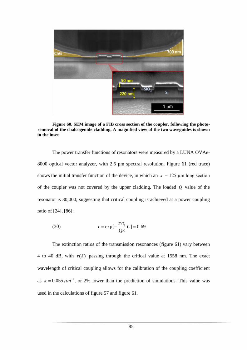
85
Figure 60. SEM image of a FIB cross section of the coupler, following the photo-
removal of the chalcogenide cladding. A magnified view of the two waveguides is shown
in the inset
The power transfer functions of resonators were measured by a LUNA OVAe-
8000 optical vector analyzer, with 2.5 pm spectral resolution. Figure 61 (red trace)
shows the initial transfer function of the device, in which an x = 125 μm long section
of the coupler was not covered by the upper cladding. The loaded Q value of the
resonator is 30,000, suggesting that critical coupling is achieved at a power coupling
ratio of [24], [86]:
(30) exp[ ] 0.69gn
r CQ
The extinction ratios of the transmission resonances (figure 61) vary between
4 to 40 dB, with ( )r passing through the critical value at 1558 nm. The exact
wavelength of critical coupling allows for the calibration of the coupling coefficient
as 10.055 m , or 2% lower than the prediction of simulations. This value was
used in the calculations of figure 57 and figure 61.
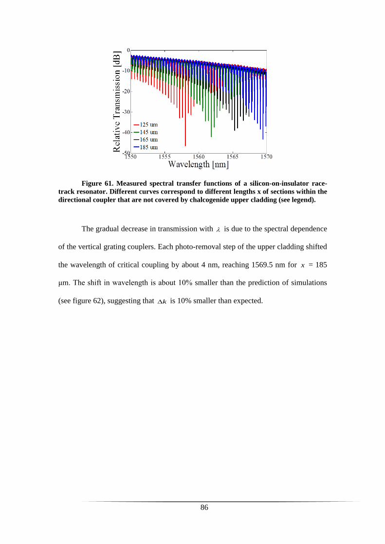
86
Figure 61. Measured spectral transfer functions of a silicon-on-insulator race-
track resonator. Different curves correspond to different lengths x of sections within the
directional coupler that are not covered by chalcogenide upper cladding (see legend).
The gradual decrease in transmission with is due to the spectral dependence
of the vertical grating couplers. Each photo-removal step of the upper cladding shifted
the wavelength of critical coupling by about 4 nm, reaching 1569.5 nm for x = 185
μm. The shift in wavelength is about 10% smaller than the prediction of simulations
(see figure 62), suggesting that k is 10% smaller than expected.
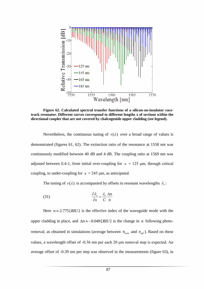
87
Figure 62. Calculated spectral transfer functions of a silicon-on-insulator race-
track resonator. Different curves correspond to different lengths x of sections within the
directional coupler that are not covered by chalcogenide upper cladding (see legend).
Nevertheless, the continuous tuning of ( )r over a broad range of values is
demonstrated (figures 61, 62). The extinction ratio of the resonance at 1558 nm was
continuously modified between 40 dB and 4 dB. The coupling ratio at 1569 nm was
adjusted between 0.4-1, from initial over-coupling for x = 125 μm, through critical
coupling, to under-coupling for x = 245 μm, as anticipated.
The tuning of ( )r is accompanied by offsets in resonant wavelengths r :
(31) r r n
x C n
Here 2.775[ ]n RIU is the effective index of the waveguide mode with the
upper cladding in place, and 0.049[ ]n RIU is the change in n following photo-
removal, as obtained in simulations (average between evenn and oddn ). Based on these
values, a wavelength offset of -0.36 nm per each 20 μm removal step is expected. An
average offset of -0.39 nm per step was observed in the measurements (figure 63), in

88
general agreement with expectations. (Note that the offset in r is close to the FSR of
the device transfer function). Small-scale variations in the offsets following
successive steps could be due to inconsistencies in step size or to angular
misalignments [92]. Specific values of r can be restored by local illumination of
short segments within the resonator loop [42], [92], if necessary (see previous
chapter).
Figure 63. Measured spectral transfer functions of a silicon-on-insulator race-
track resonator, following several steps of photo-removal of the upper cladding layer
from above the directional coupler. The lengths of the directional coupler not covered
by the uppe
The transfer function of a different device was monitored over more than 3
months following the tuning of the directional coupler (figure 64). The coupler was
200 μm long, with a section of 100 μm length initially uncovered by chalcogenide
cladding (red curve). The cladding was then removed from an additional 35 μm long
section (blue curve). The loaded Q of the device was 18,000. The photo-removal
changed the extinction ratios of the resonances near 1565 nm from 10 dB ( r = 0.3) to
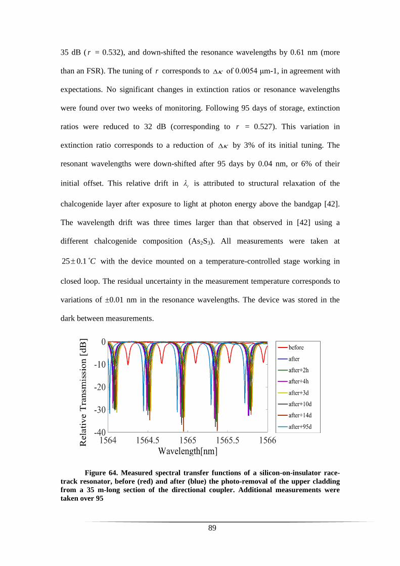
89
35 dB ( r = 0.532), and down-shifted the resonance wavelengths by 0.61 nm (more
than an FSR). The tuning of r corresponds to of 0.0054 μm-1, in agreement with
expectations. No significant changes in extinction ratios or resonance wavelengths
were found over two weeks of monitoring. Following 95 days of storage, extinction
ratios were reduced to 32 dB (corresponding to r = 0.527). This variation in
extinction ratio corresponds to a reduction of by 3% of its initial tuning. The
resonant wavelengths were down-shifted after 95 days by 0.04 nm, or 6% of their
initial offset. This relative drift in r is attributed to structural relaxation of the
chalcogenide layer after exposure to light at photon energy above the bandgap [42].
The wavelength drift was three times larger than that observed in [42] using a
different chalcogenide composition (As2S3). All measurements were taken at
25 0.1 C with the device mounted on a temperature-controlled stage working in
closed loop. The residual uncertainty in the measurement temperature corresponds to
variations of ±0.01 nm in the resonance wavelengths. The device was stored in the
dark between measurements.
Figure 64. Measured spectral transfer functions of a silicon-on-insulator race-
track resonator, before (red) and after (blue) the photo-removal of the upper cladding
from a 35 m-long section of the directional coupler. Additional measurements were
taken over 95
90
6.4 Discussion and summary
In conclusion of this chapter, the one-time, rapid and stable tuning of silicon-
photonic directional couplers over a broad range of coupling ratios, using the selective
photo-removal of a chalcogenide glass upper cladding, has been proposed, analyzed
and demonstrated. Simulations suggest that the coupling coefficient per unit length
between two partially-etched waveguides can be modified by 10%. The calculations
are supported by the experimental characterization of racetrack resonators, following
several steps of tuning. The extinction ratios of specific resonances were continuously
adjusted between 4-40 dB.
While the relatively long couplers used in experiments are strongly
wavelength dependent, this restriction is not fundamental. Analysis shows that the
photo-removal of the upper cladding may modify the coupling coefficient per unit
length between standard, fully etched waveguides by 45%. The power coupling ratio
of such devices may be adjusted between 0 and 100%, with residual wavelength
dependence that is much weaker. The length of a coupler of this type can be 50 μm
only, and may be further reduced if a smaller tuning range is sufficient.
The trimming of smaller, high-Q resonators would require high accuracy in
the removal process. The resolution step of the photo-removal setup is about 1.5 µm,
determined by the illumination spot size. A coupler such as that of figure 59, for
example, may be tuned in about 30 steps of complete removal. Finer tuning resolution
can be achieved with partial removal of the upper layer, to nonzero residual thickness.
Tuning precision is improved further with closed-loop monitoring of the device

91
transfer function during photo-removal. Yet, the applicability of the method to the
trimming of point or ultra-short couplers requires further experimental investigation.

92
Trimming of cascaded filters
7.1 Motivation
Complex cascaded integrated photonic devices are gaining much interest in
recent years due to the ability to realize high-end optical filters on small footprint
using scalable, commercial SOI technology [6]. Such filters, comprising for example
of several MZIs, find applications in the multiplexing and de-multiplexing of WDM
channels [22]. Cascaded lattice structures are also used in RF photonics signal
processing [102].
In this chapter, the trimming of phase delays, group delays and coupling
ratios, described in the previous chapters, are used in the post-fabrication tuning of the
response of cascaded MZI devices. A theoretical background on the filter transfer
function is provided first, followed by experimental demonstration of 1x4 and 1x8
channel de-multiplexers.
7.2 Theoretical background
7.2.1 Multiplexers and de-muliplexers based on cascaded MZIs.
The response of a cascaded MZIs filter can be described as the product of the
frequency-domain transfer functions of individual MZI stages. The specific cascaded
architecture considered in this work consists of MZI stages in a tree topology, with
differential path imbalances that are integer multiples of a basic unit length L . These
multiples are arranged in a geometric series: ,2 ,4L L L . A device with M stages
has 2M output ports. The primary application of these devices is in the separation of
the incoming spectrum into equal spectral channels, each appearing in a different
output port [25]. The same device may be operated in the reverse direction as well:
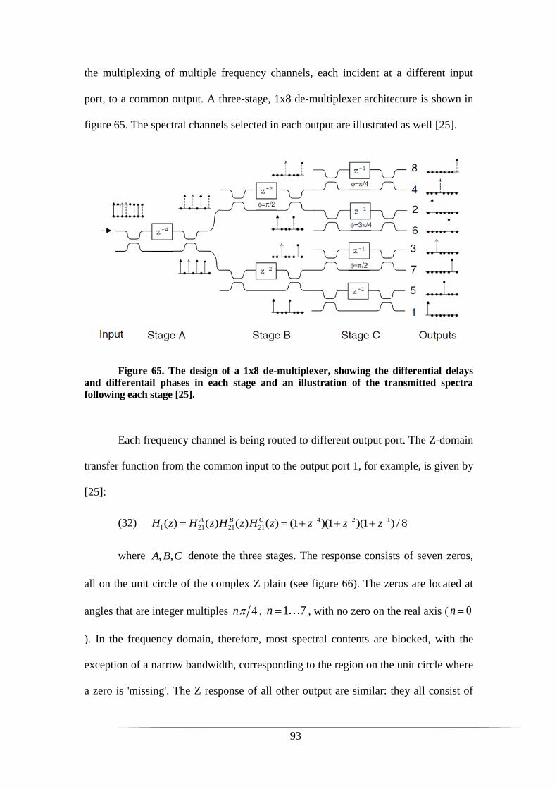
93
the multiplexing of multiple frequency channels, each incident at a different input
port, to a common output. A three-stage, 1x8 de-multiplexer architecture is shown in
figure 65. The spectral channels selected in each output are illustrated as well [25].
Figure 65. The design of a 1x8 de-multiplexer, showing the differential delays
and differentail phases in each stage and an illustration of the transmitted spectra
following each stage [25].
Each frequency channel is being routed to different output port. The Z-domain
transfer function from the common input to the output port 1, for example, is given by
[25]:
(32) 4 2 1
1 21 21 21( ) ( ) ( ) ( ) (1 )(1 )(1 ) / 8A B CH z H z H z H z z z z
where , ,A B C denote the three stages. The response consists of seven zeros,
all on the unit circle of the complex Z plain (see figure 66). The zeros are located at
angles that are integer multiples 4n , 1 7n , with no zero on the real axis ( 0n
). In the frequency domain, therefore, most spectral contents are blocked, with the
exception of a narrow bandwidth, corresponding to the region on the unit circle where
a zero is 'missing'. The Z response of all other output are similar: they all consist of

94
seven zeros on the unit circle, however the location of the 'missing' zero is different in
each port (see illustration for output port 2 in figure 65). Therefore, each output
transmits a different spectral range.
A Z domain plot of the zeros for output port 1 and 2 is given in figure 66 [25] .
Figure 66. Locations of zeros on the complex Z plain, representing the transfer
functions of the cascaded MZI channel de-multiplexer of figure 65, from the common
input to output port 1 (left) and output port 2 (right) [25].
Figure 67 [25] shows the spectral response of each stage independently,
leading to output 1.
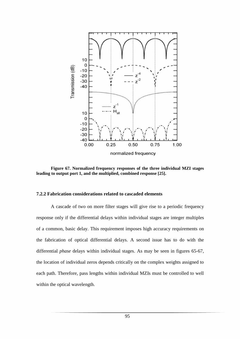
95
Figure 67. Normalized frequency responses of the three individual MZI stages
leading to output port 1, and the multiplied, combined response [25].
7.2.2 Fabrication considerations related to cascaded elements
A cascade of two on more filter stages will give rise to a periodic frequency
response only if the differential delays within individual stages are integer multiples
of a common, basic delay. This requirement imposes high accuracy requirements on
the fabrication of optical differential delays. A second issue has to do with the
differential phase delays within individual stages. As may be seen in figures 65-67,
the location of individual zeros depends critically on the complex weights assigned to
each path. Therefore, pass lengths within individual MZIs must be controlled to well
within the optical wavelength.

96
The third issue is related to the power splitting ratios of the directional
couplers that make up each MZI. The placement of all zeros on the unit circle, with
minimal passband loss, requires that all couplers are exhibit power splitting ratios of
0.5. All parameters above are subject to fabrication tolerances. In the next section we
employ our new ChG photo-trimming technique to compensate for fabrication errors
in 1x4 and 1x8 cascaded MZI Mux devices. The fabrication of these devices will put
into use the entire set of tools developed in the previous chapters.
7.3 Experimental results
7.3.1 Trimming a 1x4 cascaded MZI Mux
A 1x4 cascaded MZI was fabricated in-house on a SOI platform, using the
process described in Chapter 3. The cascaded device consisted of three individual
MZIs. Path imbalances were 1 mm and 2 mm for the two MZI stages. The MZIs were
lithographically defined in a sequential manner, one after the other, to minimize
stitching effects in the e-beam writer. Two ChG patches were deposited on the long
arms of the second-stage MZIs, in preparation for phase trimming procedure as shown
in figure 68.

97
Figure 68. Schematic layout of a 1x4, cascaded MZI channel de-multiplexer,
with ChG pathces deposited for post-fabrication trimming of phase delays.
Differential phases are defined with respect to the first-stage MZI, the one
with the largest differential delay. The path imbalance in the first MZI, at some
reference frequency 0 , equals an integer multiple of wavelengths. We refer to this
condition as 'zero differential phase'. Simulations of the four output ports (figure 69)
show that optimal channel de-multiplexing is achieved when the differential phases
within the second-stage MZIs, for the same 0 , are 1 20 ,2
. Figure 70 shows
the four measured transfer functions of the device, as-fabricated. Significant
deviations from the intended response are evident.
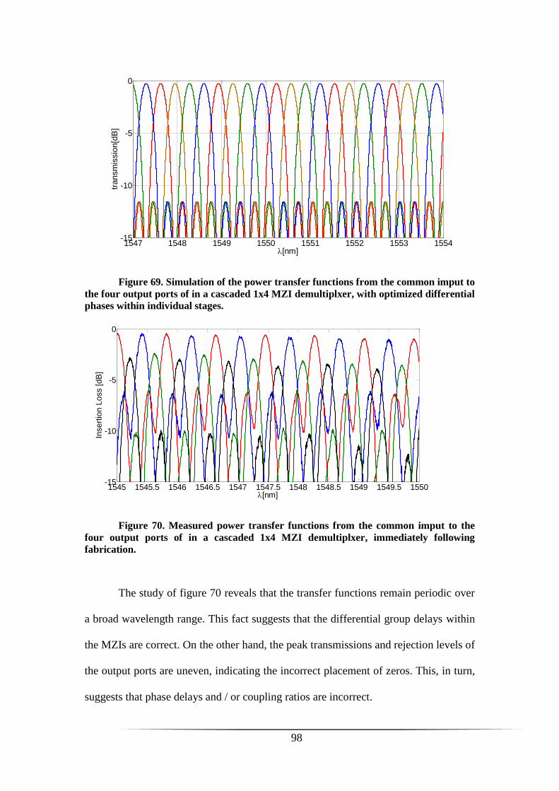
98
Figure 69. Simulation of the power transfer functions from the common imput to
the four output ports of in a cascaded 1x4 MZI demultiplxer, with optimized differential
phases within individual stages.
Figure 70. Measured power transfer functions from the common imput to the
four output ports of in a cascaded 1x4 MZI demultiplxer, immediately following
fabrication.
The study of figure 70 reveals that the transfer functions remain periodic over
a broad wavelength range. This fact suggests that the differential group delays within
the MZIs are correct. On the other hand, the peak transmissions and rejection levels of
the output ports are uneven, indicating the incorrect placement of zeros. This, in turn,
suggests that phase delays and / or coupling ratios are incorrect.
1547 1548 1549 1550 1551 1552 1553 1554-15
-10
-5
0
transm
issio
n[d
B]
[nm]
1545 1545.5 1546 1546.5 1547 1547.5 1548 1548.5 1549 1549.5 1550-15
-10
-5
0
Insert
ion L
oss [dB
]
[nm]
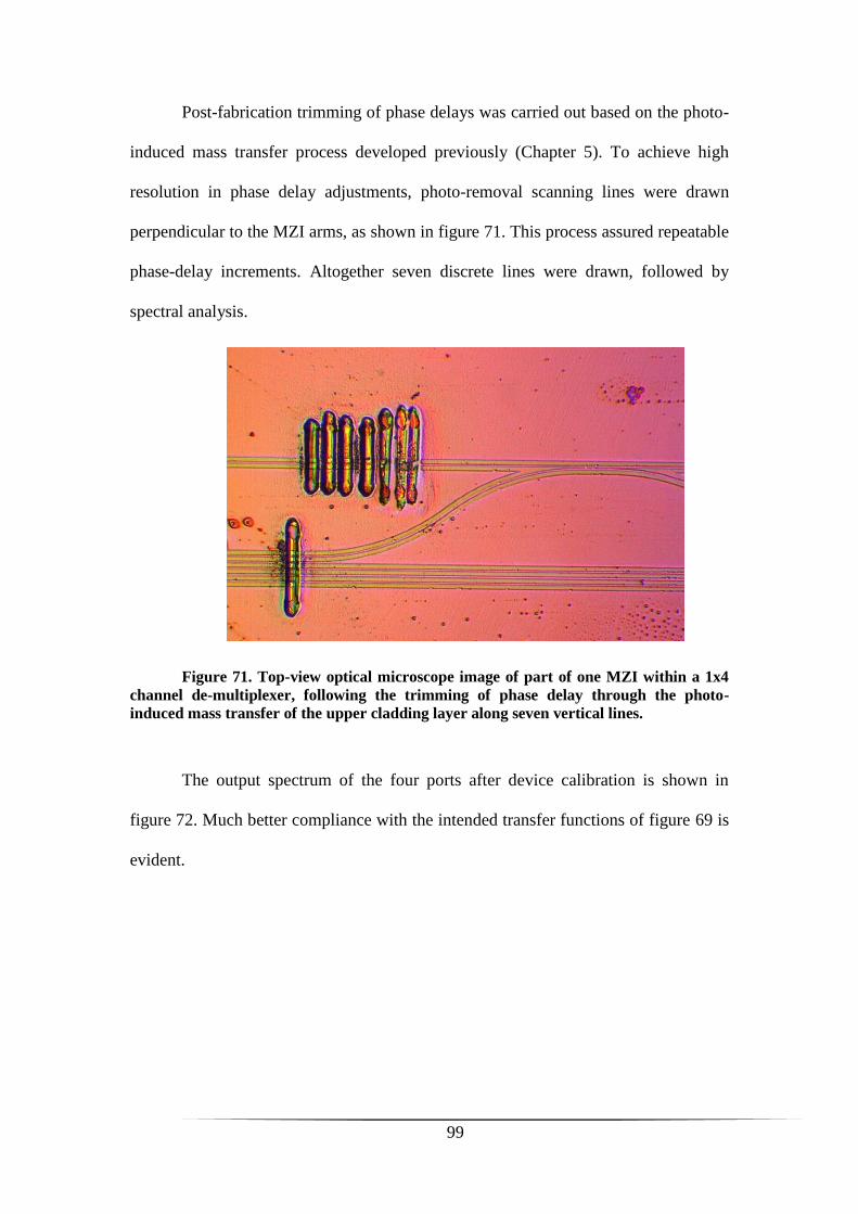
99
Post-fabrication trimming of phase delays was carried out based on the photo-
induced mass transfer process developed previously (Chapter 5). To achieve high
resolution in phase delay adjustments, photo-removal scanning lines were drawn
perpendicular to the MZI arms, as shown in figure 71. This process assured repeatable
phase-delay increments. Altogether seven discrete lines were drawn, followed by
spectral analysis.
Figure 71. Top-view optical microscope image of part of one MZI within a 1x4
channel de-multiplexer, following the trimming of phase delay through the photo-
induced mass transfer of the upper cladding layer along seven vertical lines.
The output spectrum of the four ports after device calibration is shown in
figure 72. Much better compliance with the intended transfer functions of figure 69 is
evident.

100
Figure 72. Measured power transfer functions from the common imput to the
four output ports of a cascaded 1x4 MZI demultiplxer, following the post-fabrication
trimming of differential phase delays.
7.3.2 Trimming a 1x8 cascaded MZI Mux
A 1x8 cascaded MZI channel de-multiplexer was fabricated at TowerJazz
industrial facilities, based on out design. The device requires a large footprint that is
difficult to cover in point-by-point e-beam lithography. The industrial process is based
on stepper photo-lithography with 150 nm resolution. The etching process was
developed and calibrated according to the experience gained in our in-house process.
The layout, comprised of seven MZIs, is shown in figure 73. The differential path
imbalances at the three stages of the device were 0.8 mm, 0.4 mm and 0.2 mm. Target
values of the differential phase delays within individual MZIs are noted in the
drawing as well.
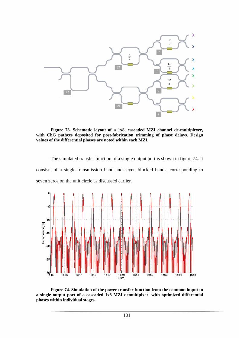
101
Figure 73. Schematic layout of a 1x8, cascaded MZI channel de-multiplexer,
with ChG pathces deposited for post-fabrication trimming of phase delays. Design
values of the differential phases are noted within each MZI.
The simulated transfer function of a single output port is shown in figure 74. It
consists of a single transmission band and seven blocked bands, corresponding to
seven zeros on the unit circle as discussed earlier.
Figure 74. Simulation of the power transfer function from the common imput to
a single output port of a cascaded 1x8 MZI demultiplxer, with optimized differential
phases within individual stages.
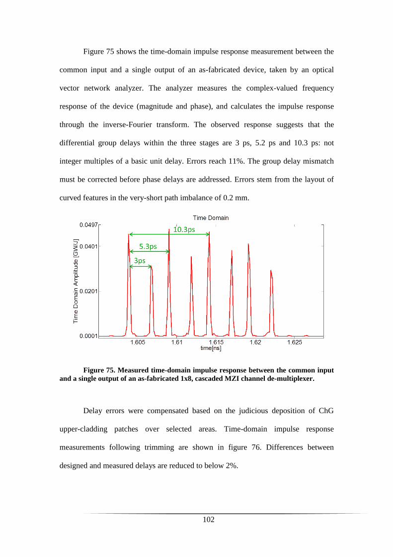
102
Figure 75 shows the time-domain impulse response measurement between the
common input and a single output of an as-fabricated device, taken by an optical
vector network analyzer. The analyzer measures the complex-valued frequency
response of the device (magnitude and phase), and calculates the impulse response
through the inverse-Fourier transform. The observed response suggests that the
differential group delays within the three stages are 3 ps, 5.2 ps and 10.3 ps: not
integer multiples of a basic unit delay. Errors reach 11%. The group delay mismatch
must be corrected before phase delays are addressed. Errors stem from the layout of
curved features in the very-short path imbalance of 0.2 mm.
Figure 75. Measured time-domain impulse response between the common input
and a single output of an as-fabricated 1x8, cascaded MZI channel de-multiplexer.
Delay errors were compensated based on the judicious deposition of ChG
upper-cladding patches over selected areas. Time-domain impulse response
measurements following trimming are shown in figure 76. Differences between
designed and measured delays are reduced to below 2%.

103
Figure 76. Measured time-domain impulse response between the common input
and a single output of a 1x8, cascaded MZI channel de-multiplexer, following the
correction of differential group delay errors within individual MZIs.
The spectral response of a single output is shown in figure 77, before (top) and
after (bottom) the trimming of phase delays within individual MZIs. The adjusted
response agrees well with the design objective. Note, however, that the frequency
response of the tuned device is slowly drifting between adjacent FSRs, due to residual
group delay inaccuracies. The responses of the remaining seven output ports were not
yet aligned.
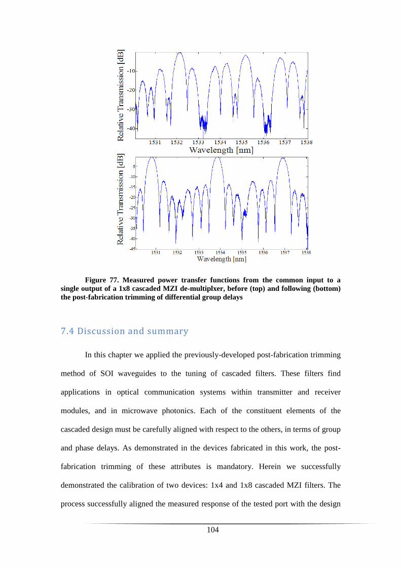
104
Figure 77. Measured power transfer functions from the common input to a
single output of a 1x8 cascaded MZI de-multiplxer, before (top) and following (bottom)
the post-fabrication trimming of differential group delays
7.4 Discussion and summary
In this chapter we applied the previously-developed post-fabrication trimming
method of SOI waveguides to the tuning of cascaded filters. These filters find
applications in optical communication systems within transmitter and receiver
modules, and in microwave photonics. Each of the constituent elements of the
cascaded design must be carefully aligned with respect to the others, in terms of group
and phase delays. As demonstrated in the devices fabricated in this work, the post-
fabrication trimming of these attributes is mandatory. Herein we successfully
demonstrated the calibration of two devices: 1x4 and 1x8 cascaded MZI filters. The
process successfully aligned the measured response of the tested port with the design

105
objective. The complete adjustment of all output ports of the 1x8 device is still under
work.
106
Optical orthogonal wavelet domain multiplexing using photonic devices
8.1 Motivation
8.1.1 Multiplexing schemes in advanced optical networks
Modern optical communication networks aggregate lower-rate data streams
from multiple users, and multiplex them together into a high bit-rate channel.
Traditionally, multiplexing in optical communication networks had been performed in
the time domain. Optical time-domain multiplexing, however, is severely restricted by
the rate of driving electronics and analog-to-digital converters. An additional
dimension is provided by wavelength division multiplexing (WDM), in which
numerous independent optical carriers are being modulated in parallel, and combined
into a single 'super channel' [103], [104]. The proper multiplexing and de-multiplexing
of WDM channels requires the assignment of 'guard bands': spectral regions that are
not used in order to eliminate cross-talk among channels. Guard bands degrade the
spectral efficiency of the network.
In recent years, more sophisticated multiplexing schemes, which are largely
employed in wireless communication, are being adapted into the realm of optical
communication. One such example is optical orthogonal frequency domain
multiplexing, or O-OFDM [105–108]. In this format, individual data streams modulate
sub-carrier tones that are equally separated in frequency. In effect, the resulting time
domain stream represents an inverse-Fourier transform of the incoming data symbols,
which are treated as though they were the Fourier coefficients of individual frequency
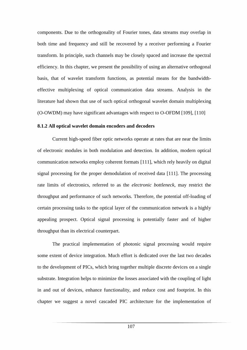
107
components. Due to the orthogonality of Fourier tones, data streams may overlap in
both time and frequency and still be recovered by a receiver performing a Fourier
transform. In principle, such channels may be closely spaced and increase the spectral
efficiency. In this chapter, we present the possibility of using an alternative orthogonal
basis, that of wavelet transform functions, as potential means for the bandwidth-
effective multiplexing of optical communication data streams. Analysis in the
literature had shown that use of such optical orthogonal wavelet domain multiplexing
(O-OWDM) may have significant advantages with respect to O-OFDM [109], [110]
8.1.2 All optical wavelet domain encoders and decoders
Current high-speed fiber optic networks operate at rates that are near the limits
of electronic modules in both modulation and detection. In addition, modern optical
communication networks employ coherent formats [111], which rely heavily on digital
signal processing for the proper demodulation of received data [111]. The processing
rate limits of electronics, referred to as the electronic bottleneck, may restrict the
throughput and performance of such networks. Therefore, the potential off-loading of
certain processing tasks to the optical layer of the communication network is a highly
appealing prospect. Optical signal processing is potentially faster and of higher
throughput than its electrical counterpart.
The practical implementation of photonic signal processing would require
some extent of device integration. Much effort is dedicated over the last two decades
to the development of PICs, which bring together multiple discrete devices on a single
substrate. Integration helps to minimize the losses associated with the coupling of light
in and out of devices, enhance functionality, and reduce cost and footprint. In this
chapter we suggest a novel cascaded PIC architecture for the implementation of

108
wavelet transform-based encoder and decoder functions [112], showing the potential
application of PICs in the all-optical realization of mathematical transforms.
8.2 Theoretical background
8.2.1 The wavelet transform
A wavelet is a waveform of effectively limited duration that has an average
value of zero. Wavelets used in signal processing tend to be irregular and asymmetric
functions. A family of wavelets can be constructed from a single mother wavelet
function . Daughter wavelets are formed by translation (parameter b )
and contraction (parameter a ) of the chosen mother function [113], [114]:
(33) , 1( )a b t bt
aa
In a similar manner to Fourier analysis, a family of wavelet functions can be
used as a basis for the decomposition of signals. Unlike Fourier analysis, however,
wavelet decomposition breaks up the signal in terms of two arguments: delay and
scale. The continuous wavelet transform (CWT) is obtained by projecting a signal
f t on daughter wavelets of continuously varying a and b values [113], [114]:
(34) *1( , ; ( ), ( )) ( )
t bC a b f t t f t dt
aa
The signal is reconstructed through multiplying each coefficient by the
appropriately scaled and shifted daughter wavelet, an operation known as the inverse
continuous wavelet transform (ICWT):
(35)
, 2
2
1 1( ) ( , ; ( ), ( )) ( )
( )
a b
ab
daf t C a b f t t t db
C aa
C d

109
Unlike the Fourier transform, the CWT conveys information on the instance in
which specific spectral components occur. Naturally, different choices of wavelet
function family would lead to an entirely different CWT. The many admissible
wavelets that can be used contribute to the strength of wavelet analysis.
8.2.2 The discrete wavelet transform (DWT)
Many situations, such as the implementation of the wavelet transform over
digital signal processing, call for the discrete version of the operation. Like CWT, the
digital wavelet transform (DWT) provides a time-scale representation of a digital
signal. DWT coefficients are usually sampled from CWT on a dyadic grid (powers of
2). The DWT is realized by a successive application of a digital high-pass filter (HPF)
of impulse response h n and a low-pass filter (LPF) of impulse response g n , with
n an integer variable, whose shapes are drawn from the specific choice of wavelet
family. Following each filtering cycle the signal is down-sampled by a factor of 2,
hence the transform analyzes the signal at different frequency bands with different
resolutions. The HPF output in each filtering stage is referred to as the detailed
information kCD n , with k the number of stage, and the corresponding LPF output
is known as the coarse approximation kCA n . The entire process is illustrated in
figure 78(a) below, and the reconstruction of the original signal s n is illustrated in
panel (b) of the figure. The relations among the normalized pass-band frequencies of
successive detailed information and the coarse approximation are shown in figure 79.
110
Figure 78. DWT (a) and IDWT tree structure. S[n] is the discrete input signal;
g[n] and h[n] are the discrete LPF and HPF used in the DWT; is the reconstructed
signal; g'[n] and h'[n] are the discrete LPF and HPF reconstruction filters used in the
IDWT.
Figure 79. DWT Spectrum division; CD[n] and CA are the n level detail
coefficients and the coarse approximation coefficients, respectively.
The impulse responses of the HPF and LPF in the DWT are strictly related
[113], [114]:
(36) [ 1 ] ( 1) [ ]ng L n h n
h[n]
2
g[n]
2
h[n]
2
g[n]
2
h[n]
2
g[n]
2
S[n]
CD3[n]
CD2[n]
CD1[n]
CA3[n]
h’[n]g'[n]
2 2
2
g'[n] h’[n]
2 2
h'[n]g'[n]
S[n]
CD1[n]
CA3[n] CD3[n]
CD2[n]
(a) (b)
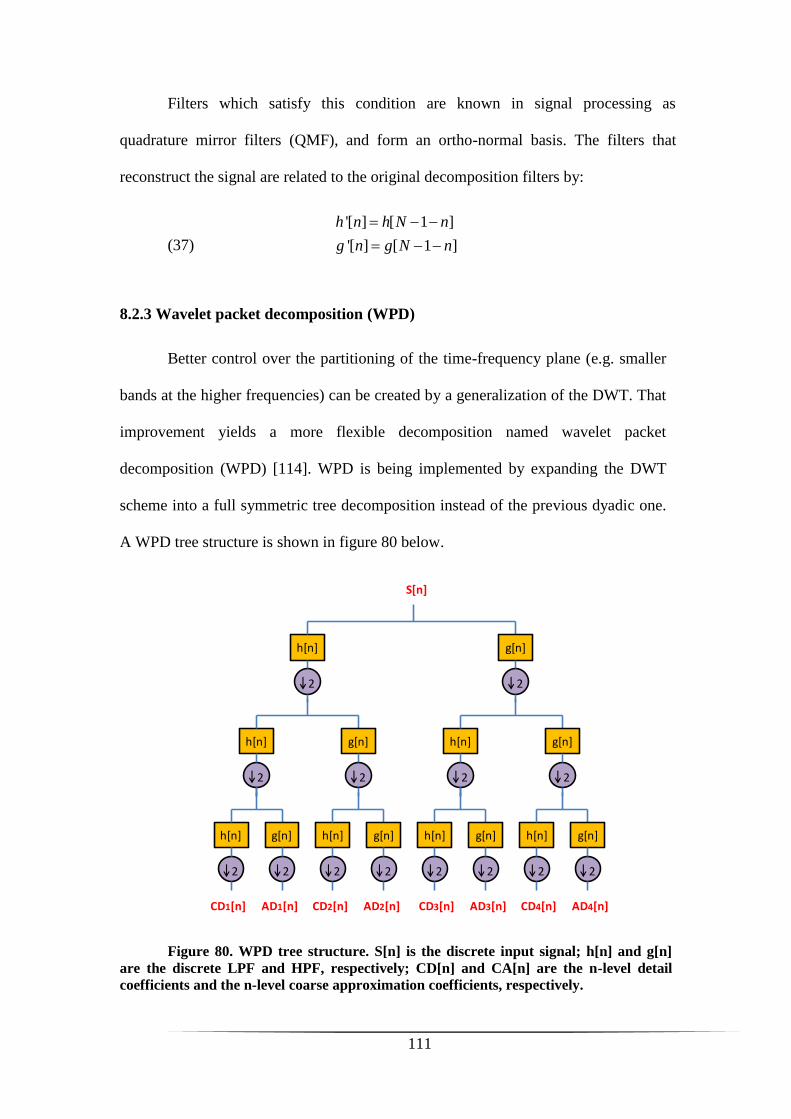
111
Filters which satisfy this condition are known in signal processing as
quadrature mirror filters (QMF), and form an ortho-normal basis. The filters that
reconstruct the signal are related to the original decomposition filters by:
(37)
'[ ] [ 1 ]
'[ ] [ 1 ]
h n h N n
g n g N n
8.2.3 Wavelet packet decomposition (WPD)
Better control over the partitioning of the time-frequency plane (e.g. smaller
bands at the higher frequencies) can be created by a generalization of the DWT. That
improvement yields a more flexible decomposition named wavelet packet
decomposition (WPD) [114]. WPD is being implemented by expanding the DWT
scheme into a full symmetric tree decomposition instead of the previous dyadic one.
A WPD tree structure is shown in figure 80 below.
Figure 80. WPD tree structure. S[n] is the discrete input signal; h[n] and g[n]
are the discrete LPF and HPF, respectively; CD[n] and CA[n] are the n-level detail
coefficients and the n-level coarse approximation coefficients, respectively.
h[n]
2
g[n]
2
S[n]
AD2[n]CD1[n]
h[n]
2
g[n]
2
h[n]
2
g[n]
2
h[n]
2
g[n]
2
h[n]
2
g[n]
2
h[n]
2
g[n]
2
h[n]
2
g[n]
2
CD2[n] CD3[n] CD4[n]AD1[n] AD3[n] AD4[n]

112
In the WPD both the detail and approximation outputs are successively
decomposed. For k levels of decomposition, the WPD produces 2k different
coefficients. Spectrum allocation of the different branches in the tree is shown in
figure 81.
Figure 81. WPD Spectrum division; CD[n] and CA[n] are the n level detail and
approximation coefficients, respectively.
DWT is mainly used for data compression (JPEG2000), image processing and
computer vision, speech recognition and biomedical applications (recognizing
abnormal phenomena) [113], [114]. Over the last few years, WPD had been proposed
as a potential underlying principle for spectrally efficient multiplexing of independent
data streams in high-end optical communication. Compared with O-OFDM, O-
OWDM could allow for a more flexible allocation of resources, due to the inherent
delay-scale freedom of the wavelet daughter functions. The same properties may help
circumvent impairments that are isolated in either time or spectrum. O-OWDM was
found to be more robust against inter-symbol interference (ISI) [109], [110]. In this
chapter we focus on a particular choice of wavelet basis, that of the Haar-wavelet
transform (see next). The concept of O-OWDM had been proposed a number of years
ago [115], and several thorough numerical analyses had been provided [110]. The
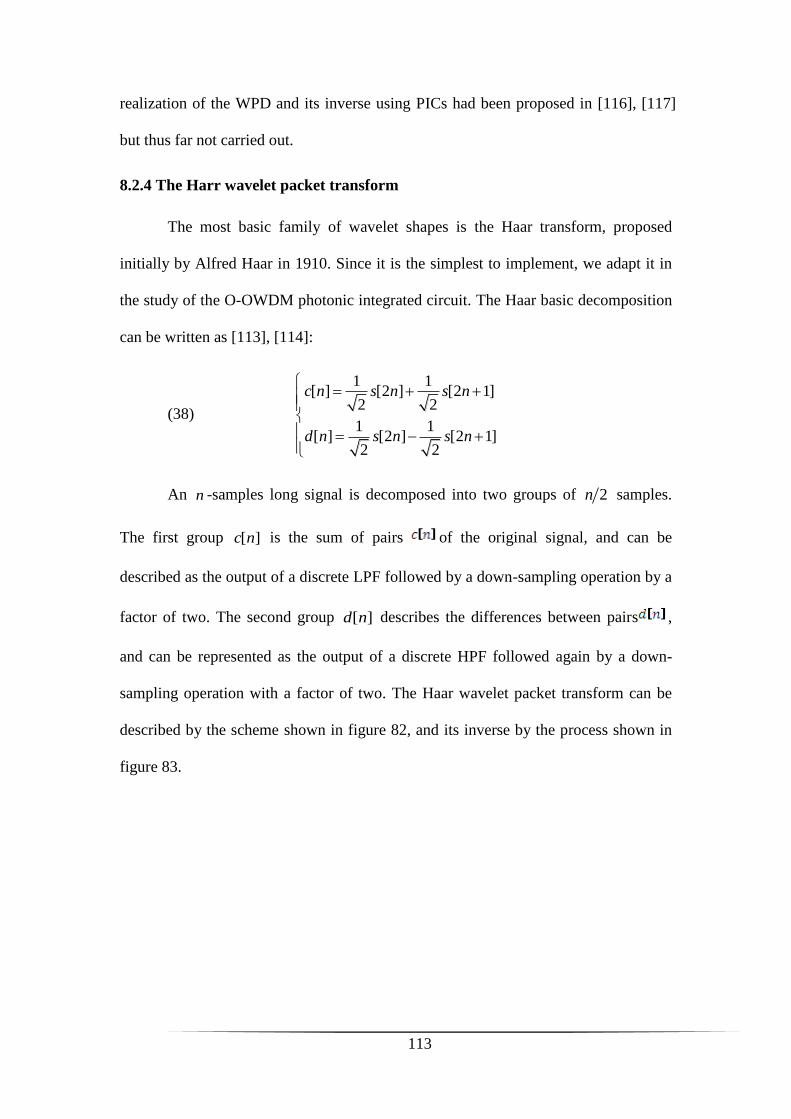
113
realization of the WPD and its inverse using PICs had been proposed in [116], [117]
but thus far not carried out.
8.2.4 The Harr wavelet packet transform
The most basic family of wavelet shapes is the Haar transform, proposed
initially by Alfred Haar in 1910. Since it is the simplest to implement, we adapt it in
the study of the O-OWDM photonic integrated circuit. The Haar basic decomposition
can be written as [113], [114]:
(38)
1 1[ ] [2 ] [2 1]
2 2
1 1[ ] [2 ] [2 1]
2 2
c n s n s n
d n s n s n
An n -samples long signal is decomposed into two groups of 2n samples.
The first group [ ]c n is the sum of pairs of the original signal, and can be
described as the output of a discrete LPF followed by a down-sampling operation by a
factor of two. The second group [ ]d n describes the differences between pairs ,
and can be represented as the output of a discrete HPF followed again by a down-
sampling operation with a factor of two. The Haar wavelet packet transform can be
described by the scheme shown in figure 82, and its inverse by the process shown in
figure 83.
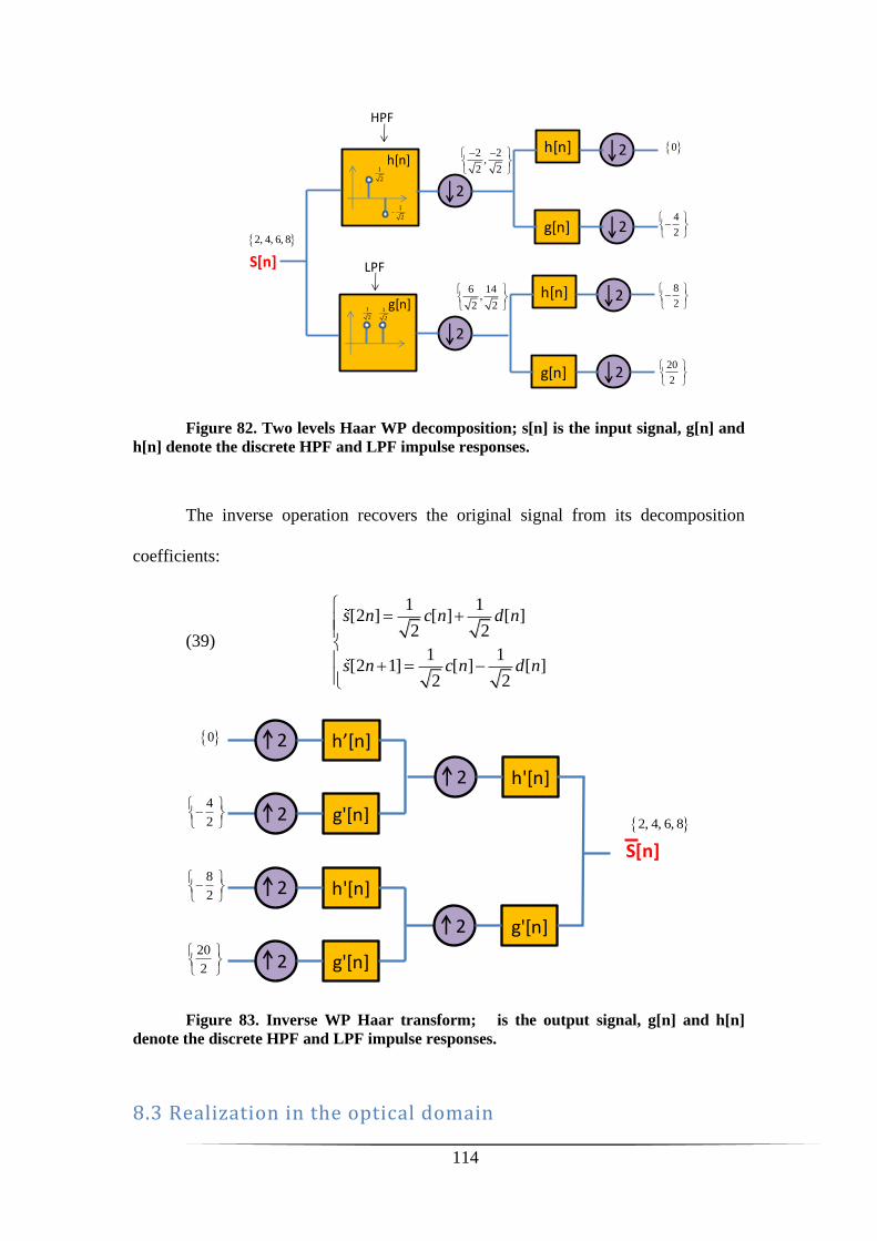
114
Figure 82. Two levels Haar WP decomposition; s[n] is the input signal, g[n] and
h[n] denote the discrete HPF and LPF impulse responses.
The inverse operation recovers the original signal from its decomposition
coefficients:
(39)
1 1[2 ] [ ] [ ]
2 2
1 1[2 1] [ ] [ ]
2 2
s n c n d n
s n c n d n
Figure 83. Inverse WP Haar transform; is the output signal, g[n] and h[n]
denote the discrete HPF and LPF impulse responses.
8.3 Realization in the optical domain
2
h[n]
S[n]
1
2
1
2
h[n]
HPF
1
2
g[n]1
2
g[n]
2
2
2
h[n]
g[n]
2
2
LPF
2, 4, 6, 8
2 2,
2 2
6 14,
2 2
8
2
20
2
0
4
2
g'[n]
2 h’[n]
S[n]
2
g'[n]
2 h'[n]
2
g'[n]
2 h'[n]
2
0
4
2
8
2
20
2
2, 4, 6, 8
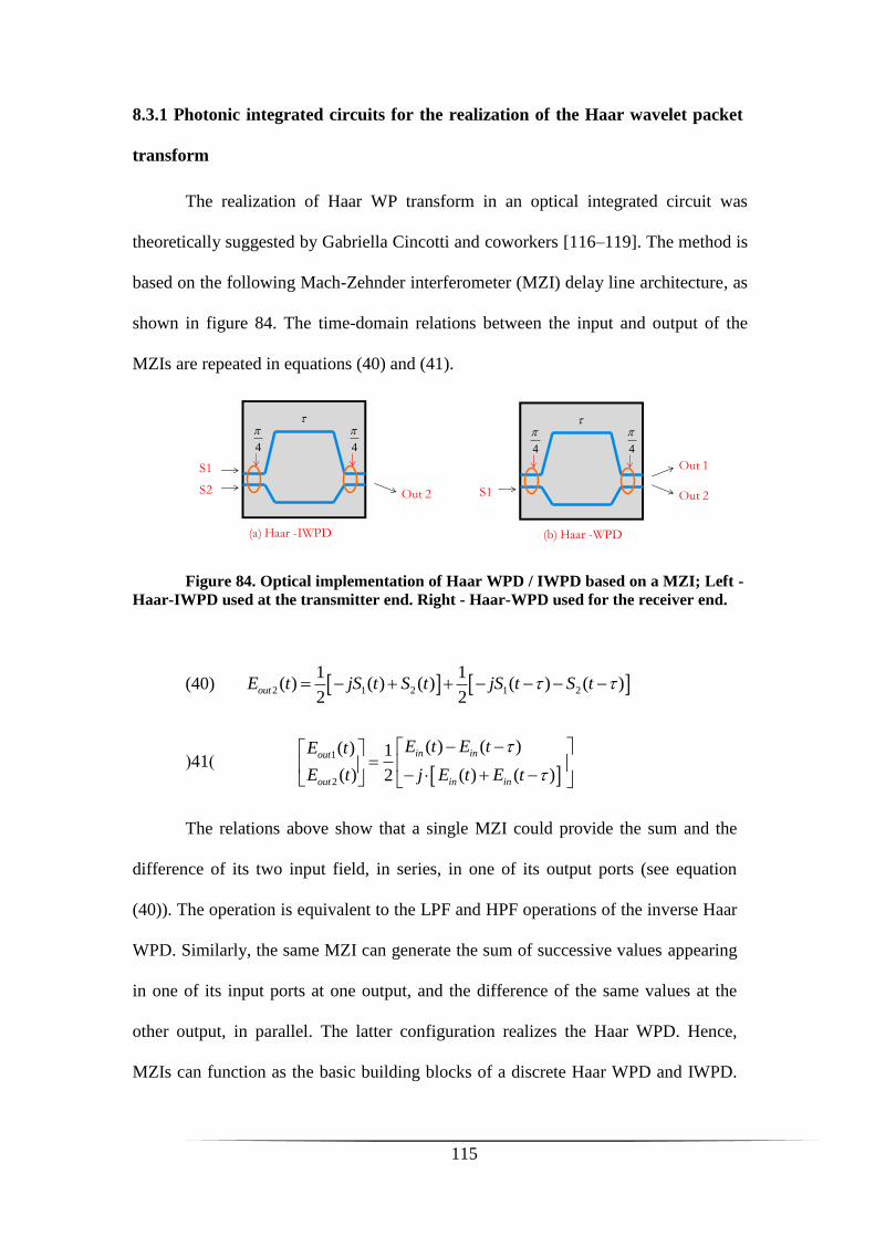
115
8.3.1 Photonic integrated circuits for the realization of the Haar wavelet packet
transform
The realization of Haar WP transform in an optical integrated circuit was
theoretically suggested by Gabriella Cincotti and coworkers [116–119]. The method is
based on the following Mach-Zehnder interferometer (MZI) delay line architecture, as
shown in figure 84. The time-domain relations between the input and output of the
MZIs are repeated in equations (40) and (41).
Figure 84. Optical implementation of Haar WPD / IWPD based on a MZI; Left -
Haar-IWPD used at the transmitter end. Right - Haar-WPD used for the receiver end.
(40) 2 1 2 1 2
1 1( ) ( ) ( ) ( ) ( )
2 2outE t jS t S t jS t S t
(41)
1
2
( ) ( )( ) 1
( ) ( ) ( )2
in inout
out in in
E t E tE t
E t j E t E t
The relations above show that a single MZI could provide the sum and the
difference of its two input field, in series, in one of its output ports (see equation
(40)). The operation is equivalent to the LPF and HPF operations of the inverse Haar
WPD. Similarly, the same MZI can generate the sum of successive values appearing
in one of its input ports at one output, and the difference of the same values at the
other output, in parallel. The latter configuration realizes the Haar WPD. Hence,
MZIs can function as the basic building blocks of a discrete Haar WPD and IWPD.
S2 Out 2
S1
4
4
(a) Haar -IWPD
S1 Out 2
4
4
Out 1
(b) Haar -WPD

116
Different wavelet bases can be implemented by using a longer MZI cascaded chain,
with unbalanced directional couplers[118], [119].
As can be seen in equations (40) and (41), the MZI realization of the WPD
includes an additional relative phase shift of 90 degrees in between the two inputs /
outputs, which is not part of the Haar formalism. This additional phase must be
compensated for. Furthermore, the optical path lengths connecting between cascaded
MZIs cannot be controlled at the fabrication stage to a sub-wavelength precision. The
proper representation of the mathematical operations in the optical domain would
require post-fabrication trimming procedures, such as those described in the previous
chapters.
8.3.2 Architectures for optical encoders and decoders representing the Haar
wavelet packet decomposition
Three-stage MZI-based PICs for the realization of Haar O-OWDM encoding
and decoding are shown in figures 85-86. The encoder calculates the inverse Haar
WPD of eight coefficients, incoming from eight parallel input values. The
reconstructed signal appears in series at the output of the circuit. Note that padding
by seven zeros is necessary between successive bits at each input, so that the
transform coefficients of one input parallel word do not overrun those of the next
word at the output [105], [120], [121]. The zero padding is the optical-domain
equivalent of the up-sampling that is part of a digital inverse WPD. Similarly, a
proper gating is necessary at the each of the eight outputs of the decoder circuit,
since the original data is only reconstructed at specific time slots within the symbol
duration [120]. The remainder of the symbol duration is occupied by noise-like inter-
symbol interference.

117
Figure 85. Schematic illustration of an all-optical Haar WP encoder used in an
optical transmitter; s1-s8 are low rate input data channels, with seven-bits zero padding.
The output is the multiplexed Haar transform signal.
Figure 86. All optical Haar WP decoder used in an optical receiver; The
incoming signal is constructed from eight data channels, which are recovered
individually at the eight outputs. The output channels must be down sampled by factor
of 8.
T/2
S2
T
S1
S3
S4
T
S5
S6
S7
S8
T T
Out
In
(MZI)
S1-S2S1+S2
S3-S4S3+S4
T/2
T/2
T/2
T/4
T/4
T/8
T
T
TT
In
WP- Encoded
8 – data Ch.
8 – Separate
data Ch.
S1
S2
S3
S4
S5
S6
S7
S8
T/8
T/4
T/4
T/2
T/2
T/2
T/2
OUT
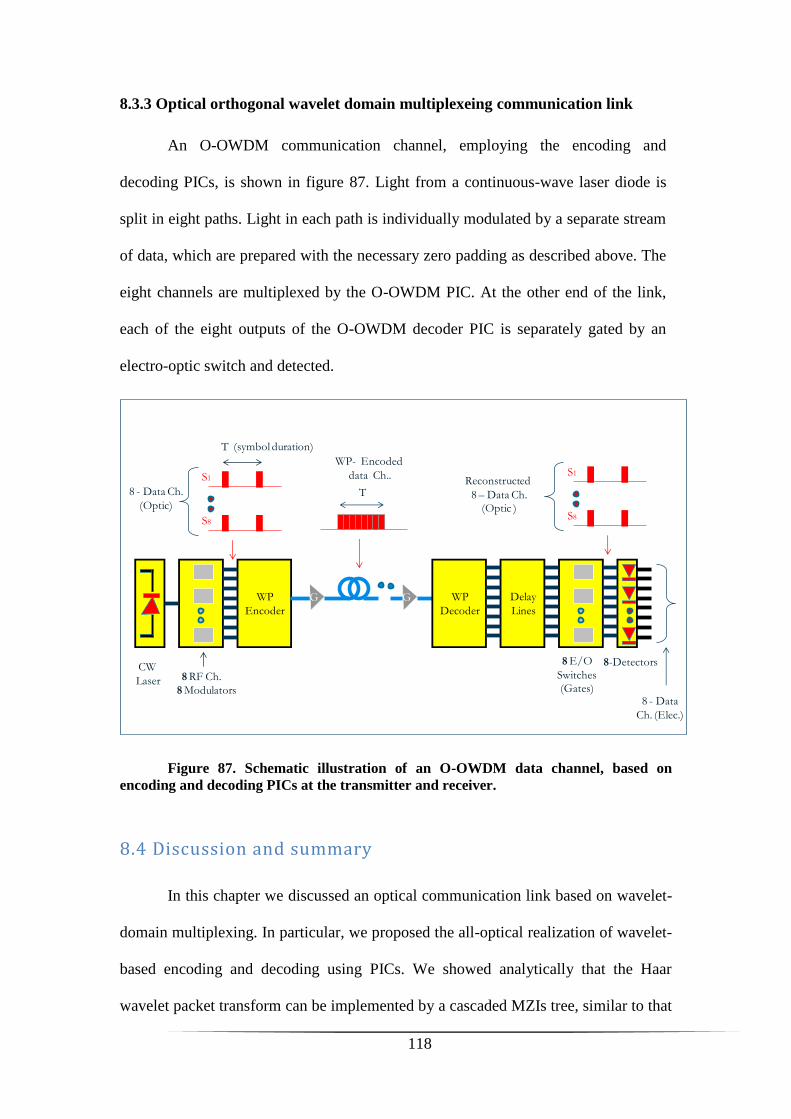
118
8.3.3 Optical orthogonal wavelet domain multiplexeing communication link
An O-OWDM communication channel, employing the encoding and
decoding PICs, is shown in figure 87. Light from a continuous-wave laser diode is
split in eight paths. Light in each path is individually modulated by a separate stream
of data, which are prepared with the necessary zero padding as described above. The
eight channels are multiplexed by the O-OWDM PIC. At the other end of the link,
each of the eight outputs of the O-OWDM decoder PIC is separately gated by an
electro-optic switch and detected.
Figure 87. Schematic illustration of an O-OWDM data channel, based on
encoding and decoding PICs at the transmitter and receiver.
8.4 Discussion and summary
In this chapter we discussed an optical communication link based on wavelet-
domain multiplexing. In particular, we proposed the all-optical realization of wavelet-
based encoding and decoding using PICs. We showed analytically that the Haar
wavelet packet transform can be implemented by a cascaded MZIs tree, similar to that
WP
Encoder
CW
Laser
T (symbol duration)
WP
Decoder
Delay
Lines
8E/O
Switches
(Gates)8Modulators
S8
S1
8 - Data Ch.
(Optic)S8
S1Reconstructed
8 – Data Ch.
(Optic )
8 - Data
Ch. (Elec.)
8RF Ch.
8-Detectors
WP- Encoded
data Ch..
T

119
of chapter 7, with a specific choice of differential phases. The all-optical approach can
potentially off-load certain processing tasks from the electronic layer, partially
relieving the electronic computation bottleneck. The proposed device can be
fabricated and tuned using the trimming methods developed in this research. The
wavelet encoders and decoders represent one example of advance passive PICs,
implementing complex mathematical operations, which could be realized based on
our techniques as part of future work.
120
Conclusions and perspective
9.1 Summary
In this research, a new method for the one-time, permanent post-fabrication
trimming of silicon-photonic devices was proposed and demonstrated experimentally.
The method relies on photo-induced modifications to an upper cladding of ChG, using
two mechanisms: changes to the layer refractive index, or photo-removal via a mass
transfer effect. The proposed method is simple and quick to implement. The upper
glass layer is considerably more stable than the photo-sensitive polymer layers
proposed elsewhere. The trimming method addresses all fundamental parameters of
PIC building blocks: phase delays, group delays and coupling ratios. High-precision
control over phase delays was achieved in a closed-loop tuning setup, with the device
connected to semi-permanent fiber holders. The response of the device could be
monitored continuously while it was being modified.
The fabrication of devices can be divided into two main parts: the silicon-
photonics platform, and the ChG upper cladding. SOI devices were fabricated in Bar-
Ilan University by e-beam lithography followed by plasma etching, or using stepper
photo-lithography and etching at an industrial facility. Next, a thin silica buffer layer
was deposited, and patch regions of ChG were defined in a photo-lithography and lift-
off process.
The method was experimentally demonstrated in the tuning of five different
components, made of partially-etched ridge SOI waveguides. Differential phase
delays within MZIs were modified using the photo-induced mass transfer. The
sensitivity of the process was 50 µrad per 1 µm of photo-removal length. Simulations

121
suggest that 2.5 times larger phase delay variations may be obtained using fully-
etched rectangular silicon waveguides instead of ridge structures.
Group index trimming was demonstrated using the photo-removal of the upper
cladding from above a 500 µm-long section of the longer arm of a MZI, with a path
imbalance of 1 mm. The FSR of the device was modified by 1%, signifying a 2%
change in the group delay index of irradiated segments. Here too, 2.5 times larger
modifications are expected using rectangular, fully-etched waveguides.
Changes to the coupling ratios of directional couplers, using cladding photo-
removal, were theoretically and numerically analyzed. Results suggest that the
coupling coefficient per unit length of couplers made of ridge waveguides and fully-
etched waveguides may be modified by as much as 10% and 45%, respectively.
Tuning was experimentally demonstrated in the trimming of 300 µm-long directional
couplers leading into race-track resonators, comprised of ridge waveguides. Photo-
removal enabled the continuous adjustment of the coupling ratio at specific
wavelengths, from over-coupling through critical coupling to negligible coupling. The
extinction ratios of individual resonances were varied between 4 – 40 dB. The transfer
function modifications remained stable following three months of storage. The
analysis shows that use of fully-etched waveguides would support the tuning of much
shorter couplers between 0-100% power transfer, with wavelength dependence that is
much reduced.
Lastly, photo-induced mass transfer was used to adjust differential phase and
group delays within individual MZIs in 1x4 and 1x8 cascaded channel de-multiplexer
filters. The post-fabrication tuning correctly aligned the transfer functions of the
devices with their intended designs. These last examples demonstrate the applicability
of the proposed technique to the fabrication of practical devices.
122
9.2 Loss mechanisms in the chalcogenide-on-SOI platform
9.2.1 Excess loss following the deposition of chalcogenide glass
The deposition of ChG upper cladding directly on top of silicon waveguide
cores resulted in large excess losses. The exact loss mechanism is not yet understood.
Possible explanations include the trapping of air bubbles in the ChG layer (although
none could be observed), or dangling bonds at the interface between ChG and Si that
form surface absorption traps at sub-bandgap energies. This problem was partially
circumvented with the deposition of a 50 nm-thick silica buffer layer, however the
buffer layer reduces the modal confinement in the upper cladding. Better
understanding of loss mechanisms would be pursued as part of future research.
9.2.2 Loss at the boundaries between covered and uncovered segments
The selective deposition of a ChG upper cladding on top of parts of the SOI
waveguide might lead to additional losses due to mode mismatch between covered
and exposed segments, as illustrated in figure 88.

123
Figure 88. Illustration of possible modal mismatch at the interface between
exposed SOI ridge waveguides and segmetns that are covered with a ChG upper
cladding.
Transmission losses due to modal mismatch may be estimated using the
overlap integral between the transverse profiles of the modes in the two regions [25]:
(42)
2*
1 2
10 2 2
1 2
[ ] 10 logarea
area area
E E dALoss dB
E dA E dA
Here 1,2E are the modal profiles in the two regions, and integration is
performed over the transverse cross-section. The field profiles for waveguides with
and without upper cladding were numerically calculated using COMSOL 2D finite
element simulation, for both ridge and full-etch geometries. Modal mismatch losses
were found to be 1% for the ridge waveguide, and 4% for the fully etched waveguide.
These losses are negligible within MZI devices, but might limit the Q-factor of high-
quality resonators.
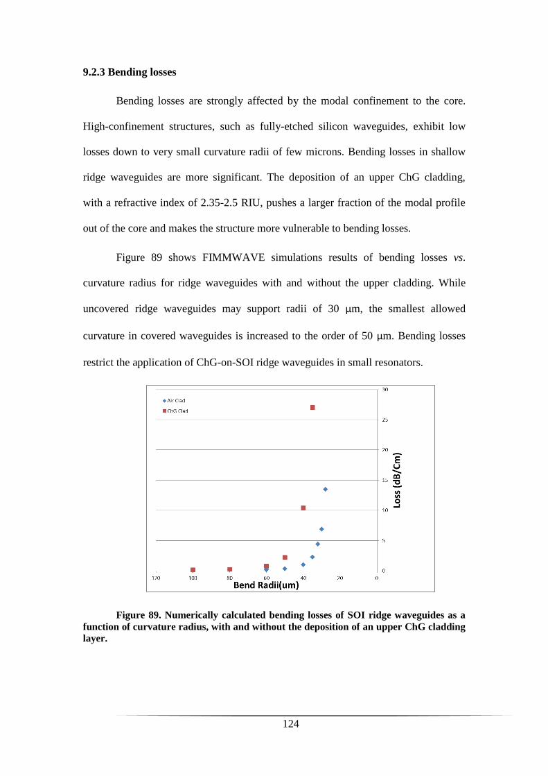
124
9.2.3 Bending losses
Bending losses are strongly affected by the modal confinement to the core.
High-confinement structures, such as fully-etched silicon waveguides, exhibit low
losses down to very small curvature radii of few microns. Bending losses in shallow
ridge waveguides are more significant. The deposition of an upper ChG cladding,
with a refractive index of 2.35-2.5 RIU, pushes a larger fraction of the modal profile
out of the core and makes the structure more vulnerable to bending losses.
Figure 89 shows FIMMWAVE simulations results of bending losses vs.
curvature radius for ridge waveguides with and without the upper cladding. While
uncovered ridge waveguides may support radii of 30 µm, the smallest allowed
curvature in covered waveguides is increased to the order of 50 µm. Bending losses
restrict the application of ChG-on-SOI ridge waveguides in small resonators.
Figure 89. Numerically calculated bending losses of SOI ridge waveguides as a
function of curvature radius, with and without the deposition of an upper ChG cladding
layer.
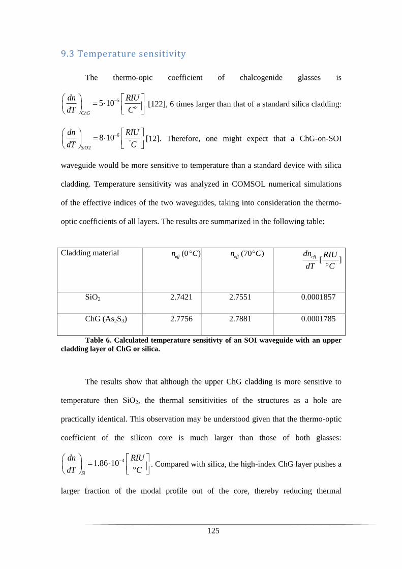
125
9.3 Temperature sensitivity
The thermo-opic coefficient of chalcogenide glasses is
55 10o
ChG
dn RIU
dT C
[122], 6 times larger than that of a standard silica cladding:
6
2
8 10SiO
dn RIU
dT C
[12]. Therefore, one might expect that a ChG-on-SOI
waveguide would be more sensitive to temperature than a standard device with silica
cladding. Temperature sensitivity was analyzed in COMSOL numerical simulations
of the effective indices of the two waveguides, taking into consideration the thermo-
optic coefficients of all layers. The results are summarized in the following table:
Cladding material (0 )effn C
(70 )effn C [ ]
effdn RIU
dT C
SiO2 2.7421 2.7551 0.0001857
ChG (As2S3) 2.7756 2.7881 0.0001785
Table 6. Calculated temperature sensitivty of an SOI waveguide with an upper
cladding layer of ChG or silica.
The results show that although the upper ChG cladding is more sensitive to
temperature then SiO2, the thermal sensitivities of the structures as a hole are
practically identical. This observation may be understood given that the thermo-optic
coefficient of the silicon core is much larger than those of both glasses:
41.86 10Si
dn RIU
dT C
. Compared with silica, the high-index ChG layer pushes a
larger fraction of the modal profile out of the core, thereby reducing thermal

126
sensitivity. This effect counter-acts the larger thermal sensitivity of the ChG layer
itself.
We therefore find that thermal drifts in ChG-on-SOI devices would be no
worse than those of standard SOI devices. Nevertheless, these thermal drifts must be
addressed. One possible solution is the stabilization of the device substrate
temperature using thermo-electric cooling (TEC). However, power consumption of
TEC is large, and cannot be tolerated in many energy-conscious applications. In fact,
the power consumption of many active-tuning methods, which do not require TEC, is
much smaller. A combination of both approaches, in which a rough calibration is
performed first using ChG layers and residual errors are corrected using active
heaters, could help reduce the power consumption of active turning even further.
In case an entirely passive solution is required, athermal designs might be used
instead. Athermal implementations combine between layers with positive and
negative thermo-optic coefficients, which largely cancel out [123], [124]. Post-
fabrication trimming using ChG upper cladding would be applicable to such designs
as well.
9.4 Stability and degradation over time
9.4.1 Sensitivity to light
The photo-sensitivity of ChG layers is employed in this work in the form of
deliberate exposure. However, the intended exposure of the same layers to ambient
light could lead to unintended drifting in the layer index and in the device transfer
function, based on the very same mechanisms. Unintended exposure may accumulate
over time. Possible solutions include the storage of devices in opaque packaging, or
the deposition of a protective layer which absorbs visible light and allows for infrared
127
transmission only. The protective layer would support the tuning of devices through
two-photon processes.
9.4.2 Chalcogenide glasses deterioration
As-deposited thin films of ChGs are different from bulk glasses in that they contain a
large fraction of homo-polar bonds (S-S or Se-Se in As2S3 and As2Se3, respectively),
and even solvents residues in case of spin coating deposition [125]. These homo-polar
bonds modify the refractive index of the layer and make it unstable, and also increase
surface roughness [125].
Annealing processes following layer deposition lead to the removal of solvent
molecules, and to structural transformations towards the “bulk state” [46]. Annealing
processes produce films with very low surface roughness, and raise the refractive
index towards that of the bulk ChG. For example, the annealing of As2Se3 at 170 °C
for 16 hours elevated its refractive index from an initial value of 2.45 RIU to 2.75
RIU at 1550 nm. The corresponding value in bulk glass is 2.83 RIU [125].
Photo-oxidation over time observed in as-deposed As2S3 layers, as a result of
exposure to short-wavelength radiation (below 248 nm), plus humidity [126]. The As-
As bonds in the as-deposited layer react with water vapors which accumulate on the
surface. Subject to the activation energy of photons a corrosion to the upper ChG
layer takes place, resulting in As2O3 arsenolite crystal. Exposure to longer-wavelength
radiation induces annealing, but not corrosion [126]. Oxidation can be avoided by
protecting the thin ChG film by an upper capping layer, such as SiO2, and avoiding
humidity and exposure to UV radiation.

128
Bibliography
[1] P. E. Green Jr, “Fiber to the home: the next big broadband thing,”
Communications Magazine, IEEE, vol. 42, no. 9, pp. 100–106, 2004.
[2] A. F. Benner, M. Ignatowski, J. A. Kash, D. M. Kuchta, and M. B. Ritter,
“Exploitation of optical interconnects in future server architectures,” IBM
Journal of Research and Development, vol. 49, no. 4.5, pp. 755–775, 2005.
[3] R. Nagarajan, D. Lambert, M. Kato, V. Lal, G. Goldfarb, J. Rahn, M. Kuntz, J.
Pleumeekers, A. Dentai, H.-S. Tsai, and others, “10 Channel, 100Gbit/s per
channel, dual polarization, coherent QPSK, monolithic InP receiver photonic
integrated circuit,” in Optical Fiber Communication Conference, 2011, p.
OML7.
[4] G. Moore, “BCramming more components onto integrated
circuits,[Electronics, vol. 38,” Apr, vol. 19, pp. 114–117, 1965.
[5] G. T. Reed and A. P. Knights, Silicon photonics: an introduction. John Wiley
& Sons, 2004.
[6] R. Soref, “The past, present, and future of silicon photonics,” Selected Topics
in Quantum Electronics, IEEE Journal of, vol. 12, no. 6, pp. 1678–1687, 2006.
[7] R. J. Baker, “Special purpose CMOS circuits,” CMOS: Circuit Design, Layout,
and Simulation, Third Edition, pp. 523–550, 2010.
[8] J. Bowers, D. Liang, A. Fang, H. Park, R. Jones, and M. Paniccia, “Hybrid
silicon lasers: The final frontier to integrated computing,” Optics and
Photonics News, vol. 21, no. 5, pp. 28–33, 2010.
[9] H. Park, A. Fang, S. Kodama, and J. Bowers, “Hybrid silicon evanescent laser
fabricated with a silicon waveguide and III-V offset quantum wells,” Optics
Express, vol. 13, no. 23, pp. 9460–9464, 2005.
[10] E. L. Wooten, K. M. Kissa, A. Yi-Yan, E. J. Murphy, D. Lafaw, P. F.
Hallemeier, D. Maack, D. V. Attanasio, D. J. Fritz, G. J. McBrien, and others,
“A review of lithium niobate modulators for fiber-optic communications
systems,” Selected Topics in Quantum Electronics, IEEE Journal of, vol. 6, no.
1, pp. 69–82, 2000.
[11] Q. Xu, B. Schmidt, S. Pradhan, and M. Lipson, “Micrometre-scale silicon
electro-optic modulator,” nature, vol. 435, no. 7040, pp. 325–327, 2005.
[12] G. Cocorullo, F. Della Corte, and I. Rendina, “Temperature dependence of the
thermo-optic coefficient in crystalline silicon between room temperature and
550 K at the wavelength of 1523 nm,” Applied physics letters, vol. 74, no. 22,
pp. 3338–3340, 1999.
[13] S. Manipatruni, Q. Xu, B. Schmidt, J. Shakya, and M. Lipson, “High speed
carrier injection 18 Gb/s silicon micro-ring electro-optic modulator,” Lasers
and Electro-Optics Society, pp. 537–538, 2007.
[14] J. Michel, J. Liu, and L. C. Kimerling, “High-performance Ge-on-Si
photodetectors,” Nature Photonics, vol. 4, no. 8, pp. 527–534, 2010.
[15] B. Charbonnier, S. Menezo, P. O‟Brien, A. Lebreton, J. Fedeli, and B. Ben
Bakir, “Silicon photonics for next generation FDM/FDMA PON,” Journal of
Optical Communications and Networking, vol. 4, no. 9, pp. A29–A37, 2012.
[16] L. Chen, C. R. Doerr, L. Buhl, Y. Baeyens, R. Aroca, and others,
“Monolithically integrated 40-wavelength demultiplexer and photodetector
129
array on silicon,” Photonics Technology Letters, IEEE, vol. 23, no. 13, pp.
869–871, 2011.
[17] A. Alduino, L. Liao, R. Jones, M. Morse, B. Kim, W.-Z. Lo, J. Basak, B.
Koch, H.-F. Liu, H. Rong, and others, “Demonstration of a high speed 4-
channel integrated silicon photonics WDM link with hybrid silicon lasers,” in
Integrated Photonics Research, Silicon and Nanophotonics, 2010, p. PDIWI5.
[18] D. Duval, A. B. González-Guerrero, S. Dante, J. Osmond, R. Monge, L. J.
Fernández, K. E. Zinoviev, C. Dom𝚤nguez, and L. M. Lechuga, “Nanophotonic
lab-on-a-chip platforms including novel bimodal interferometers, microfluidics
and grating couplers,” Lab on a Chip, vol. 12, no. 11, pp. 1987–1994, 2012.
[19] M. R. Lee and P. M. Fauchet, “Two-dimensional silicon photonic crystal based
biosensing platform for protein detection,” Optics express, vol. 15, no. 8, pp.
4530–4535, 2007.
[20] M. H. Khan, H. Shen, Y. Xuan, L. Zhao, S. Xiao, D. E. Leaird, A. M. Weiner,
and M. Qi, “Ultrabroad-bandwidth arbitrary radiofrequency waveform
generation with a silicon photonic chip-based spectral shaper,” Nature
Photonics, vol. 4, no. 2, pp. 117–122, 2010.
[21] Y. Ding, J. Xu, C. Peucheret, M. Pu, L. Liu, J. Seoane, H. Ou, X. Zhang, and
D. Huang, “Multi-channel 40 Gbit/s NRZ-DPSK demodulation using a single
silicon microring resonator,” Journal of Lightwave Technology, vol. 29, no. 5,
pp. 677–684, 2011.
[22] F. Horst, W. M. Green, S. Assefa, S. M. Shank, Y. A. Vlasov, and B. J.
Offrein, “Cascaded Mach-Zehnder wavelength filters in silicon photonics for
low loss and flat pass-band WDM (de-) multiplexing,” Optics express, vol. 21,
no. 10, pp. 11652–11658, 2013.
[23] H. Haus, W.-P. Huang, S. Kawakami, N. Whitaker, and others, “Coupled-
mode theory of optical waveguides,” Lightwave Technology, Journal of, vol. 5,
no. 1, pp. 16–23, 1987.
[24] A. Yariv, “Coupled-mode theory for guided-wave optics,” Quantum
Electronics, IEEE Journal of, vol. 9, no. 9, pp. 919–933, 1973.
[25] C. K. Madsen and J. H. Zhao, Optical filter design and analysis. Wiley-
Interscience, 1999.
[26] W. Bogaerts, P. De Heyn, T. Van Vaerenbergh, K. De Vos, S. Kumar
Selvaraja, T. Claes, P. Dumon, P. Bienstman, D. Van Thourhout, and R. Baets,
“Silicon microring resonators,” Laser & Photonics Reviews, vol. 6, no. 1, pp.
47–73, 2012.
[27] P. De Dobbelaere, B. Analui, E. Balmater, D. Guckenberger, M. Harrison, R.
Koumans, D. Kucharski, Y. Liang, G. Masini, A. Mekis, and others,
“Demonstration of first WDM CMOS photonics transceiver with
monolithically integrated photo-detectors,” in Proc. ECOC, 2008, pp. 21–25.
[28] A. Narasimha, B. Analui, E. Balmater, A. Clark, T. Gal, D. Guckenberger, S.
Gutierrez, M. Harrison, R. Koumans, D. Kucharski, and others, “A 40-Gb/s
QSFP optoelectronic transceiver in a 0.13 μm CMOS Silicon-on-Insulator
Technology,” in Optical Fiber Communication Conference, 2008, p. OMK7.
[29] B. Jalali and S. Fathpour, “Silicon photonics,” Lightwave Technology, Journal
of, vol. 24, no. 12, pp. 4600–4615, 2006.
[30] Kotura Inc. products. [Online]. Available: http://www.kotura.com/. .
[31] F. Xia, M. Rooks, L. Sekaric, and Y. Vlasov, “Ultra-compact high order ring
resonator filters using submicron silicon photonic wires for on-chip optical
interconnects,” Optics express, vol. 15, no. 19, pp. 11934–11941, 2007.
130
[32] J. E. Cunningham, I. Shubin, X. Zheng, T. Pinguet, A. Mekis, Y. Luo, H.
Thacker, G. Li, J. Yao, K. Raj, and others, “Highly-efficient thermally-tuned
resonant optical filters,” Optics Express, vol. 18, no. 18, pp. 19055–19063,
2010.
[33] P. Dong, W. Qian, H. Liang, R. Shafiiha, D. Feng, G. Li, J. E. Cunningham, A.
V. Krishnamoorthy, and M. Asghari, “Thermally tunable silicon racetrack
resonators with ultralow tuning power,” Optics express, vol. 18, no. 19, pp.
20298–20304, 2010.
[34] H. L. Lira, S. Manipatruni, and M. Lipson, “Broadband hitless silicon electro-
optic switch for on-chip optical networks,” Optics Express, vol. 17, no. 25, pp.
22271–22280, 2009.
[35] H. Haeiwa, T. Naganawa, and Y. Kokubun, “Wide range center wavelength
trimming of vertically coupled microring resonator filter by direct UV
irradiation to SiN ring core,” Photonics Technology Letters, IEEE, vol. 16, no.
1, pp. 135–137, 2004.
[36] L. Zhou, K. Okamoto, and S. Yoo, “Athermalizing and trimming of slotted
silicon microring resonators with UV-sensitive PMMA upper-cladding,”
Photonics Technology Letters, IEEE, vol. 21, no. 17, pp. 1175–1177, 2009.
[37] S. Suzuki, Y. Hatakeyama, Y. Kokubun, and S. T. Chu, “Precise control of
wavelength channel spacing of microring resonator add-drop filter array,”
Journal of lightwave technology, vol. 20, no. 4, p. 745, 2002.
[38] J. Schrauwen, D. Van Thourhout, and R. Baets, “Trimming of silicon ring
resonator by electron beam induced compaction and strain,” Optics express,
vol. 16, no. 6, pp. 3738–3743, 2008.
[39] C.-T. Wang, C.-W. Tseng, J.-H. Yu, Y.-C. Li, C.-H. Lee, H.-C. Jau, M.-C.
Lee, Y.-J. Chen, and T.-H. Lin, “Optical bistability in a silicon nitride
microring resonator with azo dye-doped liquid crystal as cladding material,”
Optics express, vol. 21, no. 9, pp. 10989–10994, 2013.
[40] A. H. Atabaki, A. A. Eftekhar, M. Askari, and A. Adibi, “Accurate post-
fabrication trimming of ultra-compact resonators on silicon,” Optics express,
vol. 21, no. 12, pp. 14139–14145, 2013.
[41] Y. Shen, I. B. Divliansky, D. N. Basov, and S. Mookherjea, “Electric-field-
driven nano-oxidation trimming of silicon microrings and interferometers,”
Optics letters, vol. 36, no. 14, pp. 2668–2670, 2011.
[42] A. Canciamilla, F. Morichetti, S. Grillanda, P. Velha, M. Sorel, V. Singh, A.
Agarwal, L. C. Kimerling, and A. Melloni, “Photo-induced trimming of
chalcogenide-assisted silicon waveguides,” Optics express, vol. 20, no. 14, pp.
15807–15817, 2012.
[43] R. W. Douglas and S. Frank, A history of glass making. GT Foulis & co., 1972.
[44] W. B. Jensen, “A note on the term" chalcogen,” Journal of chemical
education, vol. 74, no. 9, p. 1063, 1997.
[45] B. Kolomiets, “Vitreous semiconductors (I),” physica status solidi (b), vol. 7,
no. 2, pp. 359–372, 1964.
[46] B. J. Eggleton, B. Luther-Davies, and K. Richardson, “Chalcogenide
photonics,” Nature photonics, vol. 5, no. 3, pp. 141–148, 2011.
[47] A. Wells, “Structural Inorganic Chemistry (5th edn.) Clarendon.” Oxford,
1984.
[48] X. Zhang, Y. Guimond, and Y. Bellec, “Production of complex chalcogenide
glass optics by molding for thermal imaging,” Journal of Non-Crystalline
Solids, vol. 326, pp. 519–523, 2003.
131
[49] C. C. Wang, “Empirical relation between the linear and the third-order
nonlinear optical susceptibilities,” Physical Review B, vol. 2, no. 6, p. 2045,
1970.
[50] M. D. Pelusi, V. G. Ta‟eed, L. Fu, E. Mägi, M. R. Lamont, S. Madden, D.-Y.
Choi, D. A. Bulla, B. Luther-Davies, and B. J. Eggleton, “Applications of
highly-nonlinear chalcogenide glass devices tailored for high-speed all-optical
signal processing,” Selected Topics in Quantum Electronics, IEEE Journal of,
vol. 14, no. 3, pp. 529–539, 2008.
[51] J. Hu, V. Tarasov, A. Agarwal, L. Kimerling, N. Carlie, L. Petit, and K.
Richardson, “Fabrication and testing of planar chalcogenide waveguide
integrated microfluidic sensor,” Optics Express, vol. 15, no. 5, pp. 2307–2314,
2007.
[52] W. Tan, M. Solmaz, J. Gardner, R. Atkins, and C. Madsen, “Optical
characterization of a-As 2 S 3 thin films prepared by magnetron sputtering,” J.
Appl. Phys, vol. 107, no. 3, p. 033524, 2010.
[53] C. Huang, D. Hewak, and J. Badding, “Deposition and characterization of
germanium sulphide glass planar waveguides,” Optics Express, vol. 12, no. 11,
pp. 2501–2506, 2004.
[54] K. Youden, T. Grevatt, R. Eason, H. Rutt, R. Deol, and G. Wylangowski,
“Pulsed laser deposition of Ga-La-S chalcogenide glass thin film optical
waveguides,” Applied physics letters, vol. 63, no. 12, pp. 1601–1603, 1993.
[55] O. Efimov, L. Glebov, K. Richardson, E. Van Stryland, T. Cardinal, S. Park,
M. Couzi, and J. Bruneel, “Waveguide writing in chalcogenide glasses by a
train of femtosecond laser pulses,” Optical Materials, vol. 17, no. 3, pp. 379–
386, 2001.
[56] X. Gai, T. Han, A. Prasad, S. Madden, D.-Y. Choi, R. Wang, D. Bulla, and B.
Luther-Davies, “Progress in optical waveguides fabricated from chalcogenide
glasses,” Optics express, vol. 18, no. 25, pp. 26635–26646, 2010.
[57] K. Turcotte, J. Laniel, A. Villeneuve, C. Lopez, and K. Richardson,
“Fabrication and characterization of chalcogenide optical waveguides,” in
Integrated Photonics Research, 2000, p. IFH4.
[58] J.-F. Viens, C. Meneghini, A. Villeneuve, T. V. Galstian, E. J. Knystautas, M.
Duguay, K. Richardson, and T. Cardinal, “Fabrication and characterization of
integrated optical waveguides in sulfide chalcogenide glasses,” Journal of
Lightwave Technology, vol. 17, no. 7, p. 1184, 1999.
[59] S. Madden, D.-Y. Choi, D. Bulla, A. V. Rode, B. Luther-Davies, V. G. Ta‟eed,
M. Pelusi, and B. J. Eggleton, “Long, low loss etched As 2 S 3 chalcogenide
waveguides for all-optical signal regeneration,” Optics express, vol. 15, no. 22,
pp. 14414–14421, 2007.
[60] Y. Zou, D. Zhang, H. Lin, L. Li, L. Moreel, J. Zhou, Q. Du, O. Ogbuu, S.
Danto, J. D. Musgraves, and others, “High-Performance, High-Index-Contrast
Chalcogenide Glass Photonics on Silicon and Unconventional Non-planar
Substrates,” Advanced Optical Materials, vol. 2, no. 5, pp. 478–486, 2014.
[61] K. Shimakawa, A. Kolobov, and S. Elliott, “Photoinduced effects and
metastability in amorphous semiconductors and insulators,” Advances in
Physics, vol. 44, no. 6, pp. 475–588, 1995.
[62] K. Tanaka, “Photoinduced processes in chalcogenide glasses,” Current
Opinion in Solid State and Materials Science, vol. 1, no. 4, pp. 567–571, 1996.
132
[63] G. Pfeiffer, M. Paesler, and S. Agarwal, “Reversible photodarkening of
amorphous arsenic chalcogens,” Journal of non-crystalline solids, vol. 130, no.
2, pp. 111–143, 1991.
[64] K. Tanaka, K. Ishida, and N. Yoshida, “Mechanism of photoinduced
anisotropy in chalcogenide glasses,” Physical Review B, vol. 54, no. 13, p.
9190, 1996.
[65] L. Calvez, Z. Yang, and P. Lucas, “Light-induced matrix softening of Ge-As-
Se network glasses,” Physical review letters, vol. 101, no. 17, p. 177402, 2008.
[66] A. Saliminia, T. V. Galstian, and A. Villeneuve, “Optical field-induced mass
transport in As 2 S 3 chalcogenide glasses,” Physical review letters, vol. 85,
no. 19, p. 4112, 2000.
[67] P. Krecmer, A. Moulin, R. Stephenson, T. Rayment, M. Welland, and S.
Elliott, “Reversible nanocontraction and dilatation in a solid induced by
polarized light,” Science, vol. 277, no. 5333, pp. 1799–1802, 1997.
[68] S. R. Ovshinsky, “Reversible electrical switching phenomena in disordered
structures,” Physical Review Letters, vol. 21, no. 20, p. 1450, 1968.
[69] H. A. Kramers, La diffusion de la lumiere par les atomes. 1927.
[70] R. de Kronig, “On the theory of dispersion of x-rays,” JOSA, vol. 12, no. 6, pp.
547–556, 1926.
[71] J. S. Toll, “Causality and the dispersion relation: logical foundations,” Physical
Review, vol. 104, no. 6, p. 1760, 1956.
[72] N. Hô, M. C. Phillips, H. Qiao, P. J. Allen, K. Krishnaswami, B. J. Riley, T. L.
Myers, and N. C. Anheier, “Single-mode low-loss chalcogenide glass
waveguides for the mid-infrared,” Optics letters, vol. 31, no. 12, pp. 1860–
1862, 2006.
[73] S. Levy, V. Lyubin, M. Klebanov, J. Scheuer, and A. Zadok, “Stimulated
Brillouin scattering amplification in centimeter-long directly written
chalcogenide waveguides,” Optics letters, vol. 37, no. 24, pp. 5112–5114,
2012.
[74] A. Saliminia, A. Villeneuve, T. V. Galstyan, S. LaRochelle, and K.
Richardson, “First-and second-order Bragg gratings in single-mode planar
waveguides of chalcogenide glasses,” Journal of lightwave technology, vol.
17, no. 5, p. 837, 1999.
[75] K. Shemesh, Y. Kaganovskii, and M. Rosenbluh, “Fabrication of Channel
Waveguides in Chalcogenide Glass Films by a Focused Laser Beam,” in
Planar Waveguides and other Confined Geometries, Springer, 2015, pp. 111–
128.
[76] A. Zoubir, M. Richardson, C. Rivero, A. Schulte, C. Lopez, K. Richardson, N.
Hô, and R. Vallée, “Direct femtosecond laser writing of waveguides in As 2 S
3 thin films,” Optics letters, vol. 29, no. 7, pp. 748–750, 2004.
[77] A. A. Elabbar, “Glass transition in As 10 Se 90 chalcogenide glass: a kinetic
study,” Physica B: Condensed Matter, vol. 403, no. 23, pp. 4328–4332, 2008.
[78] K. Tanaka and K. Shimakawa, Amorphous chalcogenide semiconductors and
related materials. Springer Science & Business Media, 2011.
[79] M. Bruel, “Process for the production of thin semiconductor material films.”
Google Patents, 1994.
[80] K. Reinhardt and W. Kern, Handbook of silicon wafer cleaning technology.
William Andrew, 2008.
133
[81] M. Pu, L. Liu, H. Ou, K. Yvind, and J. M. Hvam, “Ultra-low-loss inverted
taper coupler for silicon-on-insulator ridge waveguide,” Optics
Communications, vol. 283, no. 19, pp. 3678–3682, 2010.
[82] T. Shoji, T. Tsuchizawa, T. Watanabe, K. Yamada, and H. Morita, “Low loss
mode size converter from 0.3 μm square Si wire waveguides to singlemode
fibres,” Electronics Letters, vol. 38, no. 25, pp. 1669–1670, 2002.
[83] D. Taillaert, P. Bienstman, and R. Baets, “Compact efficient broadband grating
coupler for silicon-on-insulator waveguides,” Optics letters, vol. 29, no. 23,
pp. 2749–2751, 2004.
[84] D. Vermeulen, S. Selvaraja, P. Verheyen, G. Lepage, W. Bogaerts, P. Absil, D.
Van Thourhout, and G. Roelkens, “High-efficiency fiber-to-chip grating
couplers realized using an advanced CMOS-compatible silicon-on-insulator
platform,” Optics express, vol. 18, no. 17, pp. 18278–18283, 2010.
[85] D. K. Sparacin, S. J. Spector, and L. C. Kimerling, “Silicon waveguide
sidewall smoothing by wet chemical oxidation,” Journal of lightwave
technology, vol. 23, no. 8, p. 2455, 2005.
[86] L.-W. Luo, G. S. Wiederhecker, J. Cardenas, C. Poitras, and M. Lipson, “High
quality factor etchless silicon photonic ring resonators,” Optics express, vol.
19, no. 7, pp. 6284–6289, 2011.
[87] P. Dumon, W. Bogaerts, V. Wiaux, J. Wouters, S. Beckx, J. Van Campenhout,
D. Taillaert, B. Luyssaert, P. Bienstman, D. Van Thourhout, and others, “Low-
loss SOI photonic wires and ring resonators fabricated with deep UV
lithography,” IEEE Photonics Technology Letters, vol. 16, no. 5, pp. 1328–
1330, 2004.
[88] P. Dong, W. Qian, S. Liao, H. Liang, C.-C. Kung, N.-N. Feng, R. Shafiiha, J.
Fong, D. Feng, A. V. Krishnamoorthy, and others, “Low loss shallow-ridge
silicon waveguides,” Optics express, vol. 18, no. 14, pp. 14474–14479, 2010.
[89] M. Frumar, A. Firth, and A. Owen, “Reversible photodarkening and structural
changes in As2S3 thin films,” Philosophical Magazine B, vol. 50, no. 4, pp.
463–475, 1984.
[90] S. Levy, M. Klebanov, and A. Zadok, “High-Q ring resonators directly written
in As 2 S 3 chalcogenide glass films,” Photonics Research, vol. 3, no. 3, pp.
63–67, 2015.
[91] W. A. Zortman, D. C. Trotter, and M. R. Watts, “Silicon photonics
manufacturing,” Optics express, vol. 18, no. 23, pp. 23598–23607, 2010.
[92] R. Califa, Y. Kaganovskii, D. Munk, H. Genish, I. Bakish, M. Rosenbluh, and
A. Zadok, “Large photo-induced index variations in chalcogenide-on-silicon
waveguides,” Optics letters, vol. 39, no. 20, pp. 5905–5908, 2014.
[93] E. A. Chandross, A. Hale, V. J. Kuck, E. J. Laskowski, C. K. Madsen, R. E.
Scotti, and J. Shmulovich, “Tunable directional optical waveguide couplers.”
Google Patents, 1999.
[94] F. Gan, T. Barwicz, M. Popovic, M. Dahlem, C. Holzwarth, P. Rakich, H.
Smith, E. Ippen, and F. Kartner, “Maximizing the thermo-optic tuning range of
silicon photonic structures,” in Photonics in Switching, 2007, pp. 67–68.
[95] S. Ibrahim, N. K. Fontaine, S. S. Djordjevic, B. Guan, T. Su, S. Cheung, R. P.
Scott, A. T. Pomerene, L. L. Seaford, C. M. Hill, and others, “Demonstration
of a fast-reconfigurable silicon CMOS optical lattice filter,” Optics express,
vol. 19, no. 14, pp. 13245–13256, 2011.
134
[96] T. Yasuda, Y. Tsuji, and M. Koshiba, “Tunable light propagation in photonic
crystal coupler filled with liquid crystal,” Photonics Technology Letters, IEEE,
vol. 17, no. 1, pp. 55–57, 2005.
[97] L. Zhou and A. W. Poon, “Fano resonance-based electrically reconfigurable
add-drop filters in silicon microring resonator-coupled Mach-Zehnder
interferometers,” Optics letters, vol. 32, no. 7, pp. 781–783, 2007.
[98] S. Lambert, W. De Cort, J. Beeckman, K. Neyts, and R. Baets, “Trimming of
silicon-on-insulator ring resonators with a polymerizable liquid crystal
cladding,” Optics letters, vol. 37, no. 9, pp. 1475–1477, 2012.
[99] G. Maxwell, R. Kashyap, B. Ainslie, D. Williams, and J. Armitage, “UV
written 1.5 μm reflection filters in single mode planar silica guides,”
Electronics Letters, vol. 28, no. 22, pp. 2106–2107, 1992.
[100] Y. Shen, I. B. Divliansky, D. N. Basov, and S. Mookherjea, “Perfect set-and-
forget alignment of silicon photonic resonators and interferometers,” in Optical
Fiber Communication Conference, 2011, p. PDPC3.
[101] A. Chen, V. Chuyanov, F. I. Marti-Carrera, S. Garner, W. H. Steier, S. S. Mao,
Y. Pa, L. R. Dalton, and Y. Shi, “Trimming of polymer waveguide Y-junction
by rapid photobleaching for tuning the power splitting ratio,” Photonics
Technology Letters, IEEE, vol. 9, no. 11, pp. 1499–1501, 1997.
[102] S. S. Djordjevic, L. Luo, S. Ibrahim, N. K. Fontaine, C. Poitras, B. Guan, L.
Zhou, K. Okamoto, Z. Ding, M. Lipson, and others, “Fully reconfigurable
silicon photonic lattice filters with four cascaded unit cells,” Photonics
Technology Letters, IEEE, vol. 23, no. 1, pp. 42–44, 2011.
[103] I. Kaminow, T. Li, and A. E. Willner, Optical fiber telecommunications VB:
systems and networks. Academic press, 2010.
[104] G. Keiser, Optical fiber communications. Wiley Online Library, 2003.
[105] D. Hillerkuss, R. Schmogrow, T. Schellinger, M. Jordan, M. Winter, G. Huber,
T. Vallaitis, R. Bonk, P. Kleinow, F. Frey, and others, “26 Tbit s-1 line-rate
super-channel transmission utilizing all-optical fast Fourier transform
processing,” Nature Photonics, vol. 5, no. 6, pp. 364–371, 2011.
[106] W. Shieh, Q. Yang, and Y. Ma, “107 Gb/s coherent optical OFDM
transmission over 1000-km SSMF fiber using orthogonal band multiplexing,”
Optics express, vol. 16, no. 9, pp. 6378–6386, 2008.
[107] P. Winzer, A. Gnauck, C. Doerr, M. Magarini, and L. Buhl, “Spectrally
efficient long-haul optical networking using 112-Gb/s polarization-multiplexed
16-QAM,” Lightwave Technology, Journal of, vol. 28, no. 4, pp. 547–556,
2010.
[108] X. Yi, N. K. Fontaine, R. P. Scott, and S. Yoo, “Tb/s coherent optical OFDM
systems enabled by optical frequency combs,” Journal of Lightwave
Technology, vol. 28, no. 14, pp. 2054–2061, 2010.
[109] Ö. Bulakci, M. Schuster, C.-A. Bunge, B. Spinnler, and N. Hanik, “Wavelet
transform based optical OFDM,” in Optical Fiber Communication Conference,
2009, p. OTuO6.
[110] A. Li, W. Shieh, and R. S. Tucker, “Wavelet packet transform-based OFDM
for optical communications,” Lightwave Technology, Journal of, vol. 28, no.
24, pp. 3519–3528, 2010.
[111] G. Li, “Recent advances in coherent optical communication,” Advances in
optics and photonics, vol. 1, no. 2, pp. 279–307, 2009.
[112] Y. Ben-Ezra, D. Brodeski, A. Zadok, R. Califa, and B. Lembrikov, “1 Tbps
transmission system based on hierarchical approach to Wavelet Packet

135
Transform OFDM,” in Transparent Optical Networks (ICTON), 2011 13th
International Conference on, 2011, pp. 1–4.
[113] I. Daubechies and others, Ten lectures on wavelets, vol. 61. SIAM, 1992.
[114] S. Mallat, A wavelet tour of signal processing. Academic press, 1999.
[115] T. Olson, D. Healy, and U. Österberg, “Wavelets in optical communications,”
Computing in science & engineering, vol. 1, no. 1, pp. 51–57, 1999.
[116] G. Cincotti, “Full optical encoders/decoders for photonic IP routers,” Journal
of lightwave technology, vol. 22, no. 2, p. 337, 2004.
[117] G. Cincotti, M. S. Moreolo, and A. Neri, “Optical wavelet signals processing
and multiplexing,” EURASIP Journal on Applied Signal Processing, vol. 2005,
pp. 1574–1583, 2005.
[118] M. S. Moreolo and G. Cincotti, “Compact low-loss planar architectures for all-
optical wavelet signal processing,” in Transparent Optical Networks, 2005,
Proceedings of 2005 7th International Conference, 2005, vol. 1, pp. 319–322.
[119] M. S. Moreolo, G. Cincotti, and A. Neri, “Synthesis of optical wavelet filters,”
Photonics Technology Letters, IEEE, vol. 16, no. 7, pp. 1679–1681, 2004.
[120] D. Hillerkuss, T. Schellinger, R. Schmogrow, M. Winter, T. Vallaitis, R. Bonk,
A. Marculescu, J. Li, M. Dreschmann, J. Meyer, and others, “Single Source
Optical OFDM Transmitter and Optical FFT Receiver Demonstrated at Line
Rates of 5.4 and 10.8 Tbit/s,” in National Fiber Optic Engineers Conference,
2010, p. PDPC1.
[121] D. Hillerkuss, M. Winter, M. Teschke, A. Marculescu, J. Li, G. Sigurdsson, K.
Worms, S. Ben Ezra, N. Narkiss, W. Freude, and others, “Simple all-optical
FFT scheme enabling Tbit/s real-time signal processing,” Optics express, vol.
18, no. 9, pp. 9324–9340, 2010.
[122] M. Yaman, H. Kondakci, and M. Bayindir, “Large and dynamical tuning of a
chalcogenide Fabry-Perot cavity mode by temperature modulation,” Optics
express, vol. 18, no. 3, pp. 3168–3173, 2010.
[123] B. Guha, B. B. Kyotoku, and M. Lipson, “CMOS-compatible athermal silicon
microring resonators,” Optics Express, vol. 18, no. 4, pp. 3487–3493, 2010.
[124] J. Teng, P. Dumon, W. Bogaerts, H. Zhang, X. Jian, X. Han, M. Zhao, G.
Morthier, and R. Baets, “Athermal Silicon-on-insulator ring resonators by
overlaying a polymer cladding on narrowed waveguides,” Optics express, vol.
17, no. 17, pp. 14627–14633, 2009.
[125] Y. Zou, H. Lin, O. Ogbuu, L. Li, S. Danto, S. Novak, J. Novak, J. D.
Musgraves, K. Richardson, and J. Hu, “Effect of annealing conditions on the
physio-chemical properties of spin-coated As 2 Se 3 chalcogenide glass films,”
Optical Materials Express, vol. 2, no. 12, pp. 1723–1732, 2012.
[126] P. Allen, B. Johnson, and B. Riley, “Photo-oxidation of thermally evaporated
As2S3 thin films,” J. Optoelec. Adv. Mater, vol. 7, pp. 1759–1764, 2005.

א
תקציר
התקנים נתהקט לש האופטית, תקשורתה בתחום רחבה מגמה קיימת האחרון בעשור
הסיליקוני. השבב ברמת ממוזערותו משולבות למערכות ממדים וגדולות בדידות ומערכות
עתידיות במערכות ,לדוגמא ,משובצים להיות יוכלו שכאלו ממוזערים פוטונים מעגלים
מידע לעיבוד כאמצעי ניידים, התקניםבו מחשבים בשרתי סרט רחבות אופטית לתקשורת
החומרים פלטפורמת אפליקציות. במגוון אופטיים חישה כאמצעי או מהיר בקצב אופטי
זה מצע .(SOI) מבודד גבי-על סיליקון נהיה שכאלו פוטונים רכיבים למימוש כיום המועדפת
אופטיים רכיבים שייצור כך האלקטרוניקה, בתעשיית רב זמן מזה רחב שבשימו נמצא
מתאפיין סיליקון כן כמו .יחסי באופן ונוח נגיש ,זול הינו זו קיימת תשתית על בהתבסס
האופטית התקשורת בתדרי גבוהה( )שקיפות מאוד נמוכים אינהרנטיים בהפסדים
אור הולכת מאפשר אשר (,סיליקה) התחתון המצע כלפי גבוה שבירה מקדמי ובקונטרסט
חסרונות מספר בחובו טומן בסיליקון השימוש מאידך, .יחסית קטן חתך שטח בעלי במבנים
ליניאריים לא אפקטים של עדרםיה בגביש: היחידה תא של הסימטריה מתכונות נובעיםה
תמשמעותי פוגם אשר עקיף אנרגיה פער של וקיומו ,POCKELS אפקט כדוגמת שני מסדר
.מאולצת פליטה תהליכי של ביעילותם
של פטיותוהא בדרכים רב דיוק דורש שבב על אינטגרליים אופטיים רכיבים של תכנון
מצריכות אלו מדויקות אופטיות דרכים ס"מ. מספר של לאורך להגיע עשויים אשר ,הגל מוליכי
בקווי אפילו תאפשרי האינ אשר בודדים, ננומטרים של ברמה הייצור פרמטרי על שליטה
קיזוז צורךל ,ייצורה לאחר כיול מנגנון נחוץ כן על ביותר. המתקדמים המסחריים הייצור
האופטיים. הפרמטרים של שגיאות
פלטפורמת על גל מוליכי של ייםאופט אורכים לקיזוז שיטות מספר כיום קיימות
אקטיביים במנגנונים הנעזרות שיטות עיקריות: קטגוריות לשתי לחלק יתןנ אותן ,סיליקון
השיטות .פעמי חד בכוונון המתאפיינות פאסיביות כיול ושיטות מתמשכת, לשליטה הניתנות
מוליכים םמחימו כתוצאה הסיליקון של שבירה מקדם שינוי על מבוססות ברובן האקטיביות
למוליך חופפים אשר P-I-N לצמתי מטען נושאי הזרקת על או ,הגל מוליך בקרבת מתכתיים
נוספים מורכבים ייצור שלבי מכילות אך גבוהים, בדיוקים כיול משיגות אלו שיטות .הגל

ב
פעמי חד כיול מציעות ,זאת לעומת ,פאסיביות שיטות .סגור בחוג מתמדת בקרה ומחייבות
בהם או המצע לטמפרטורת רגיש אינו הרכיב בהם יםרבמק וזול פשוט פתרון ומהוות
רגישה ציפוי שכבת על ותמתבסס רבות פאסיביות קיזוז שיטות .מבוקרת המצע טמפרטורת
כךבו ,זו שכבה של השבירה מקדם את לשנות ניתן צריבה באמצעות הגל. מוליך מעל לאור
פולימרים םניה כציפוי המשמשים החומרים מרבית הגל. מוליך של האופטית הדרך את לכייל
פתרונות על מתבססות אחרות פאסיביות שיטות זמן. לאורך יציבים שאינם אורגניים
.ישימים אינם אשר ,לקטרוניםא קרן באמצעות לחץ יצירת וא ,פלאזמהב איכול כגון מורכבים
כיול נדרש לעיתים אולם ,בלבד הפאזה השהיית בתיקון עוסקות שהוזכרו השיטות כל ,בנוסף
ההספק חלוקת יחס או הגל מוליך לאורך החבורה השהיית כגון נוספים אופטיים פרמטרים של
הקיימות. השיטות במסגרת נידונו לא אלו פרמטרים .(הצימוד מקדם) כיווני במצמד
,מדויקת ,מהירה פאסיבית קיזוז שיטת פיתוח היתה הנוכחי במחקר העיקרית המטרה
התכונות כלל מענה תספק רשא ,סיליקון מבוססי אופטיים רכיבים עבור ציבהוי זולה
אופטיים. במצמדים חלוקהה יחסו חבורה השהיית פאזה, השהיית הנדרשות: האופטיות
זכוכיות של תרכובות המשלבת חדשה היברידית בפלטפורמה התמקדנו המחקר במסגרת
הסיליקון רכיבי גבי על כמעטה לאור, רגישות (CHALCOGENIDE GLASSES) לקוגניותק
הקיימים.
מבין אחד המכילים אמורפיים למחצה מוליכים של משפחה ןניה תואלקוגניק זכוכיות
הולך אלו זכוכיותב השימוש מעבר. מתכות בצירוף ,ריוםווטל סלניום גופרית, יסודותה
,מולקולארית רוסקופיהלספקט המשמש הארוכים הגל אורכי בתחום שקיפותן משום ומתרחב
תרכובות להארה. גבוהה ורגישות אופטית, ליניאריות-אי מקדמי של גבוהים ערכים
גל באורכי הארהמ כתוצאה שלהם השבירה מקדם את לשנות מסוגלות מסוימות לקוגניותקא
עשויה אחרות תרכובות של גבוהה בעוצמה הארה ,בנוסף שלהן. האנרגיה לפער המתאימים
אופטית קרינה של הבליע ,אלו במקרים הזכוכית. שכבת במבנה גיאומטריים םיישינול להביא
,(GLASS TRANSITION) החומר של הזגוגית המעבר לטמפרטורת מעבר נקודתי לחימום גורמת
.יותר הקרים השוליים אל הקרן מרכז של החם מהאזור החומר של ולהסעה
לכייל מנת על שהוזכרו לאור שותיהרג מנגנוני בשני שימוש נעשה הנוכחי במחקר
שכבת של השבירה מקדם שינוי ידי על ראשית :מסיליקון פוטוניים ברכיבים אופטיות תכונות
הגל. מוליך מעל הזכוכית שכבת של מלאה הסרה באמצעות שניתו הגל, מוליך מעל זכוכיתה

ג
הסרה באמצעות בסיסים אופטיים רכיבים מספר של כיול למעשה הלכה בוצע המחקר במהלך
בסיסי טרימאינרפרו התקן באמצעות הודגמו חבורהוה פאזהה בהשהיית םשינויי .מלאה
(MACH-ZEHNDER INTERFEROMETER - MZI). באינדקס 2% של שינויים הושגו זה בניסוי
.RIDGE WAVEGUIDE מסוג חלקית מאוכל גל במוליך החבורה
תלותב ,סימולציה ובאמצעות תיאורטית נותח אופטי במצמד הצימוד מקדם של שינוי
ליחידת הצימוד במקדם אפשריים שינויים על מצביעות התוצאות הגל. מוליך של הבגיאומטרי
באופן מאוכלים גל מוליכיב 01%-ו ,מלא באופן מאוכלים גל במולכי 54% של בשיעור אורך
שינוי כאשר ,RING RESONATOR מסוג מהוד בהתקן למעשה הלכה הודגם האפקט .חלקי
מוחלטת וחסימה העברה בין ומעבר הקריטית הצימוד מנקודת ויציאה כניסה איפשר המצמד
משורשרים משולבים מעגליםב יושמה הכיול שיטת ,לסיכום .ספציפיים גל באורכי ההתקן של
אלו מורכבים מעגלים של התקינה פעילותם אלמנטים(. 7 )עד MZI אלמנטי מספר המכילים
למצוא יכולים אלו מעגלים בשרשרת. השונים האלמנטים בין קפדני פאזות כיול מחייבת
. אופטית תקשורת במערכות ערוצים של והפרדה בריבוב ,לדוגמא ,שימוש

תכן עניינים
I.................................................................................................באנגלית תקציר
1.................................................................................................................. מבוא1
1...............................?מדוע והיכן 6על סיליקוןממוזערים מעגלים פוטונים 1.1
3..........סיליקון..........................................במסננים והתקנים פאסיביים 1.1
12...סיליקון.......................................בשגיאות ייצור בהתקנים פוטוניים 1.3
11...סקירת שיטות כיול של רכיבים פוטוניים לאחר ייצור.......................... 1.1
12.......מטרת המחקר......................................................................... 1.1
14.............................נית על סיליקוןגלקוקפלטפורמת פוטונית מבוססת זכוכית 1
14.........לקוגניות.......................................................קמה הן זכוכיות 1.1
32...............................................קלקוגניותאפקטיים אופטיים בזכוכיות 1.1
33...על גבי התקנים פוטוניים מסיליקון................... זכוכית קלקוגניתציפוי 1.3
31...................................................................................................תהליך הייצור 3
31צור של התקנים פוטוניים מבוססי סיליקון.............................תהליך היי 3.1
34על גבי רכיבי הסיליקון............זכוכית קלקוגנית תהליך הייצור של ציפוי 3.1
11.............................................................................ת הרכיביםאריז 3.3
11..................................................................................התקנים כיול ואפיון של 1
11...........................באמצעות צימוד אנכי.רכיבים פיון ימעבדתי לא ךמער 1.1
15.....................................פיון של רכיבים פאסיביים בסיליקון..........יא 1.1
12........................קלקוגניתהמתבסס על הסרת זכוכית רכיבים כיול מערך 1.3
59...............................................כיול מקדם שבירה אפקטיבי ואינדקס חבורה 1
59......מוטיבציה...................................................................... 1.1

60..וסימולציות..................... תיאורטיפאזה ניתוח 6לכוונוןמנגנונים 1.1
67.......תיאורטי וסימולציות...............אינדקס חבורה ניתוח 6כיוונון 1.3
70תוצאות ניסיוניות................................................................... 1.1
76........דיון בתוצאות וסיכום....................................................... 1.1
78...........................................................................................כיול מצמד אופטי 2
78..............................................מוטיבציה................................ 2.1
79...ניתוח תיאורטי וסימולציות.................................................... 2.1
83....תוצאות ניסיונית................................................................. 2.3
90....כום..........................................................דיון בתוצאות וסי 2.1
51........................................................שרשרת מסננים אינטרפרומטרייםכיול 3
51.......מוטיבציה....................................................................... 3.1
92......רקע תיאורטי................................................................... 3.1
96.....תוצאות ניסיונית................................................................ 3.3
104.....דיון בתוצאות וסיכום....................................................... 3.1
106...............................בסיס התמרות וייבלט-ערוצים על מרבבלרכיב הצעה 4
106.......מוטיבציה.................................................................... 4.1
108....רקע תיאורטי.................................................................. 4.1
115.....מימוש אופטי של מסנן הוויבלט......................................... 4.3
118................דיון בשיטה המוצעת וסיכום................................... 4.1
120....................................................................................סיכום תוצאות ודיון 5
120...סיכום העבודה................................................................ 5.1
111.....................................................יםניתוח של מנגנוני הפסד 5.1
111..........................................ניתוח רגישות לטמפרטורת סביבה 5.3
112.......יציבות לאורך זמן........................................................ 5.1

114..................................................................................................רשימת מקורות
...א.......................................................................................תקציר בעברית

אבי פרופ' של בהדרכתו נעשתה המחקר תעבוד
אילן-בר אוניברסיטתב להנדסה מהפקולטה צדוק

פוטוניים רכיבים של ייצור לאחר כיול
עליונה זכוכית שכבת באמצעות בסיליקון
לאור רגישה
חיבור לשם קבלת התואר "דוקטור לפילוסופיה"
כליפה רן מאת:
להנדסה הפקולטה
אילן-בר אוניברסיטת של לסנאט הוגש
תשע"ו חשוון גן רמת