Embed Size (px)
Citation preview
Silicon Labs Quality and Operations OverviewM A R C H 2 0 1 8

Corporate Overview
Development Process
Qualification Process
Manufacturing Process
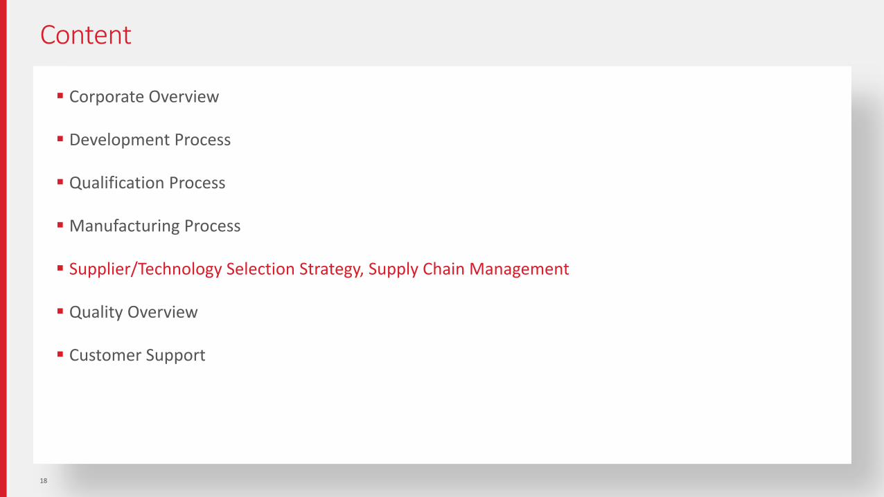
Supplier/Technology Selection Strategy, Supply Chain Management
Quality Overview
Customer Support
Content
2

Corporate Overview
Click here for Silicon Labs’ Corporate Overview homepage
Quality and Environmental Information
Highlights
ISO Certificates
Sony Green Partner Certificate
Quarterly Quality & Reliability Report
Additional information here
Investor Relations, Annual Report and Recent News
Click here for Silicon Labs’ Investor Overview homepage
Corporate Identity
3

Corporate Overview
Development Process
Qualification Process
Manufacturing Process
Supplier and Technology Selection Strategy
Quality Overview
Customer Support
Content
4

Concept & Planning
•Customer
•Sales
•Design & Apps
•Manufacturing
Design
•Analog & Digital
•Software
•Test
Verification
•Applications
•Qualification
•Customer Sampling
•Launch
Production
•Foundry
•Assembly
•Test
•Pack & Ship
New Product Development Major Milestones
5

Product Development & Release to Manufacturing follows a rigorous process with Management Review & Approval at key milestones
Product Development Process Concept, Architecture, Design and PG (Tapeout) – reviews and checklists at each stage
Release to Manufacturing (RTM) Process Pre-Production > Initial Production > Full Production
Formal reviews and checklists at each stage
Ship quantity limits increase with each phase
RTM addresses the following (not inclusive)
Probe – HW and SW
Final Test – HW and SW
Qualification
Validation & Verification
Test Optimization, offshore transfer
Cpk and statistical baselines for maverick lot detection
Product Development & Release to Manufacturing
6
Every design is reviewed to assure robust manufacturability, testability, and cost optimization
Any risks identified are removed or minimized by methods such as:
Design changes
Extra qualification
Improved manufacturing capability or controls
Increased monitoring
Reviews are held at the following milestones at a minimum
Project approval/Architecture
Pre-PG
Initial Production
Design for Cost, Test and Manufacturing
7
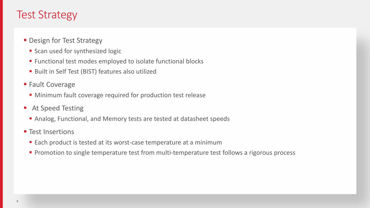
Design for Test Strategy
Scan used for synthesized logic
Functional test modes employed to isolate functional blocks
Built in Self Test (BIST) features also utilized
Fault Coverage
Minimum fault coverage required for production test release
At Speed Testing
Analog, Functional, and Memory tests are tested at datasheet speeds
Test Insertions
Each product is tested at its worst-case temperature at a minimum
Promotion to single temperature test from multi-temperature test follows a rigorous process
Test Strategy
8

Corporate Overview
Development Process
Qualification Process
Manufacturing Process
Supplier and Technology Selection Strategy
Quality Overview
Customer Support
Content
9

Product and Process Qualification & Criteria
Silicon Labs uses industry standard test methods to evaluate products and follows the guidelines of:
EIA/JESD 47 - Stress-Test-Driven Qualification of Integrated Circuits
AEC-Q100 - Stress Qualification For Integrated Circuits
Quality
Reliability
Product Performance
Product
Wafer Process
Packaging and Assembly
Qualification Process
• Assembly & Test Manufacturability
• Qualification Data By Similarity
• Product Testing Qualification
• Reliability Test Qualification
• Product Characterization
10
Customer AssuredNew or Changed

Corporate Overview
Development Process
Qualification Process
Manufacturing Process
Supplier/Technology Selection Strategy, Supply Chain Management
Quality Overview
Customer Support
Content
11

SBLs are used at these process steps
Foundry Wafer Acceptance Test (WAT)
Wafer Probe
Final Electrical Test
Limits are established to identify abnormal (maverick) material lots
Limits are based on overall yields or on specific tests or test groups
The MRP system automatically places on hold lots that fail to meet limits
There are two levels of hold/notification
Level 1 – Engineering: held for product engineer investigation and validation before release
Level 2 – MRB: held for product engineer and quality manager investigation and validation before release
Statistical Bin Limits (SBL)
12

Device packages are marked with a product identification number and a tracecode captured in our ERP system
Tracecode is also marked on the packing labels
Tracecode provides a link to the processing history, from wafer number to shipment
Product Traceability
EXAMPLE: Si4763-A30-AM
• Package Type: 40L-QFN-6x6 • Mark Method: Laser • Logo: None• Tracecode Type: Standard • Pin 1 Mark: Circle = 0.90mm diameter (Bottom-Left-Justified) • Font Size (mm): 0.70mm Right-Justified • Line 1 Mark Format: Device Number 4763A30 • Line 2 Mark Format: TTTTTT = Mfg Code (from the Assembly PO) • Line 3 Mark Format:
• YY = Year of the packaging/assembly start • WW = Work Week of the packaging/assembly start
13
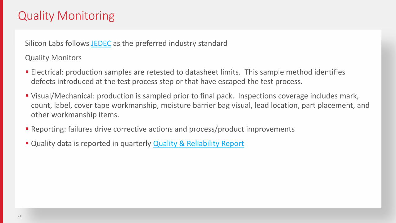
Silicon Labs follows JEDEC as the preferred industry standard
Quality Monitors
Electrical: production samples are retested to datasheet limits. This sample method identifies defects introduced at the test process step or that have escaped the test process.
Visual/Mechanical: production is sampled prior to final pack. Inspections coverage includes mark, count, label, cover tape workmanship, moisture barrier bag visual, lead location, part placement, and other workmanship items.
Reporting: failures drive corrective actions and process/product improvements
Quality data is reported in quarterly Quality & Reliability Report
Quality Monitoring
14
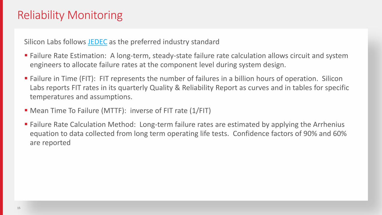
Silicon Labs follows JEDEC as the preferred industry standard
Failure Rate Estimation: A long-term, steady-state failure rate calculation allows circuit and system engineers to allocate failure rates at the component level during system design.
Failure in Time (FIT): FIT represents the number of failures in a billion hours of operation. Silicon Labs reports FIT rates in its quarterly Quality & Reliability Report as curves and in tables for specific temperatures and assumptions.
Mean Time To Failure (MTTF): inverse of FIT rate (1/FIT)
Failure Rate Calculation Method: Long-term failure rates are estimated by applying the Arrhenius equation to data collected from long term operating life tests. Confidence factors of 90% and 60% are reported
Reliability Monitoring
15

Critical to Quality (CTQ) parameters are controlled by Silicon Labs’ assembly partners
Their performance is reported quarterly in CpK reports and reviewed by the Silicon Labs Supplier Managers
Process Control Points
Process CTQ Parameter
Wire BondWire pull strength (g)Ball shear strength (g)
Lead plating Thickness (μ”)
Saw/Singulation Package Dimension (mm)
16
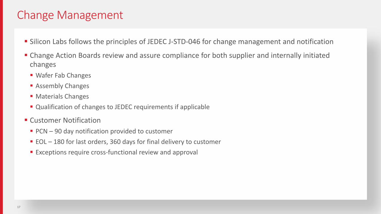
Silicon Labs follows the principles of JEDEC J-STD-046 for change management and notification
Change Action Boards review and assure compliance for both supplier and internally initiated changes
Wafer Fab Changes
Assembly Changes
Materials Changes
Qualification of changes to JEDEC requirements if applicable
Customer Notification
PCN – 90 day notification provided to customer
EOL – 180 for last orders, 360 days for final delivery to customer
Exceptions require cross-functional review and approval
Change Management
17
Corporate Overview
Development Process
Qualification Process
Manufacturing Process
Supplier/Technology Selection Strategy, Supply Chain Management
Quality Overview
Customer Support
Content
18

Partner with world-class suppliers
Manage products from development to customer delivery
Support unexpected surges in demand
Reliable, high volume supply
Quality-centered assembly and test
Dual sourced for capacity assurance
ISO9001/14001, certified company and conforms to ISO/TS 16949
Supply Chain Process Overview
19

Global Supply Chain
• Taiwan
• China
• USA
• Europe
• Singapore
Wafer Fab
• Taiwan
• China
• Malaysia
Bump / Probe • Taiwan
• Korea
• Malaysia
• Thailand
• China
• Singapore
• Philippines
Assembly / Test
• Taiwan
• Korea
• China
• Malaysia
• Thailand
• Singapore
• USA
Drop Ship
• Distributors
• Direct customers
• Hubs
Customers
>20k customers>20 distributors
20

TSMC, SMIC
& others
ASE, SPIL
& others
ASE, KYEC
& others
FAB ASSEMBLY TEST & SHIP
100% outsource >90% outsource
IC Manufacturing Model- Fabless and Outsourced
21

Delta, CDTech, Ryder, USI &
others
Components PCB ASSEMBLY TEST & SHIP
100% outsource
Module Manufacturing Model – Outsourced Assembly
22
Silicon Labs ICs & Third Party
Suppliers
Contract Manufacturers and Silicon Labs
Intl.
>90% outsource>90% outsource

Process technology, package choice and test platforms are carefully chosen based on:
Technology availability and maturity at suppliers
Technology roadmap of suppliers
Technology reliability of suppliers
Past and present execution (quality, cycle time, deliveries, operational efficiencies) from suppliers
Material cost from the supplier and
Cost of doing business with that supplier
Technology choices are made during development phase
Silicon Labs provides a second source when appropriate to ensure continuity of supply
Supplier & Technology Selection
23

Asia-based Assembly and Test Supplier Management Provides Supplier initial Evaluation, Selection, and on-going Assessment
Performs Semiannual Strategic Business Reviews (SBRs) with key suppliers to review overall business, market trends, performance, cost reduction, capacity plans, product roadmaps and specific projects
Austin-based Foundry Engineering manages the above for the wafer fab suppliers
Key Suppliers are audited at least annually
Quality management systems (ISO9001 and TS 16949)
Environmental, Health & Safety (including ISO14001)
Social Accountability (RBA (formerly EICC) Code of Conduct)
Business parameters (delivery, cost, service, capacity)
Technology
Self assessment from a supplier is occasionally deemed adequate
Supplier Management
24

Supplier Quality Assurance Monitoring Process
Outsourcing of Manufacturing Process Quality Assurance
• Defect Density
• FMEA / Control Plan
• In-coming Material Control
• SPC Monitoring
• Cpk Data Analysis
• Wafer Sort Probe Yield Monitoring
• Wafer Reliability Monitoring
Wafer
Fab & SortAssembly Final Test Pack & Ship
• DOE
• FMEA / Control Plan
• In-coming Material Control
• SPC Monitoring
• Cpk Data Analysis
• Critical to Process / Product Monitoring
• Assembly Yield Monitoring
• Reliability Monitoring
• Product Characterization
• FMEA / Control Plan
• Test Program / Revision Control
• SPC Monitoring
• Test Yield Monitoring
• QA Electrical Gate ppm
• Reliability Monitoring
• Outgoing Visual Mechanical Gate ppm
• FMEA / Control
• Shipping Label Information Accuracy
25

Silicon Labs conducts formal, monthly forecast meetings
Distributors/Sales/Representatives required to give 12-month rolling forecast secured from Customers
Forecast provides base line for Silicon Labs supply chain
Drives material starts, such as wafer
Triggers capacity planning activities
Identifies gaps in supply / demand
Provides demand snap-shot for inventory management
Provides supply / demand snap-shot for product / process management (e.g., PCN planning)
Supplier commitments input into the planning system
Commitment is measured to On Time Delivery to First Commit Date in SAP
Real-time B2B process flows with key Suppliers and Distributors
Supply Chain Planning Process Overview
26

Demand
Demand monitoring performed on an on-going, daily basis
Review of backlog against the build plan
Build plan adjustments made in real time to manage changes at the Customer/part level
Supply Chain Metrics
On time delivery to the Customer Requested Dock Date
On time delivery to the First Commit Date
Units committed vs. units produced
Cycle time
Early warning (Planned Finish Date <> Scheduled Commit Date)
Demand/Supply Performance
27

Receive weekly POS reports from Distributor
Includes shipments, backlog and forecast
Monitor inventory at Distributor monthly
Daily/Weekly communication with Distributor on current issues
Provide latest delivery dates to Distributors on demand via reporting portal
Silicon Labs Distribution Support
Customer Support - Distribution
Distributor Customer
Reduced Cycle
Time
Assembly and Test
Mainstream
Digital CMOS
Wafer Fab
28

Supply Chain Process Overview
Customer
Demand Plan Consensus
Supply Disconnects
Operations Plan
Revenue and Shipment Plan (Units, $)
PlanningMonthly
Order Scheduling
Orders
Delivery Commitments
Forecast, Backlog
Execution
Manufacturing Requirements
Supply / Demand Review
Factory Schedules
Probe Assembly Test
Inventory
BacklogCDP
SCPWafer
Customer Allocation
Daily Execution : AR ReleaseMonthly Execution
Trigger Wafer start
Weekly Execution
29

Packing media available: tape & reel, tray and tube
All finished goods are packed in a vacuum sealed Moisture Barrier Bag (MBB), including a Humidity
Indicator Card (HIC) and desiccant
Labels are automatically printed from the ERP System (SAP)
Handling Units (HUs) may not contain more than two Batches
Packing & Labeling
Reel / MBB Inner Box / HU Label Outer Box Shipping Label
Customer or Silicon Labs P/N Supplier Address
Handling Unit # Customer Address
Date Code / Trace Code Customer or Silicon Labs P/N
Seal Date Handling Unit #
Assembly Country Assembly Country
Quantity Quantity
MSL, Reflow Temperature, Bake Time, RoHS, “HF” and “Pb-Free” (if applicable) & Plating Type (e#)
“RoHS”, “HF” and “Pb-Free” symbol (if applicable)
30

Corporate Overview
Development Process
Qualification Process
Manufacturing Process
Supplier/Technology Selection Strategy, Supply Chain Management
Quality Overview
Customer Support
Content
31

Registered to ISO 9001 since Jun’00 (link)
Registered to ISO14001 since Dec’06 (link)
Certified Sony Green Partner since Aug’08 (link)
Quality & Environmental Systems
Quality Policy Silicon Labs is committed to total customer satisfaction by: Providing differentiated products, solutions and services for a more connected world Exceeding customer needs through innovation and simplicity Continually improving our world-class quality management system
Environmental PolicyAt Silicon Labs, we manage environmental matters as an integral part of our business by our commitment to: Designing, marketing, and selling environmentally friendly products, Continually improving our environmental performance and pollution prevention, Complying with applicable legal and other requirements that relate to our environmental aspects, and Minimizing the negative environmental impact of our business activities.
32

Department Head
VP of Quality & Central Engineering
Director of Quality & Corporate Test Engineering
Quality Engineering Director
Quality & Environmental Systems Manager
Supplier & Asia Quality Manager
Device Analysis Lab Manager
Location
Austin
Singapore
Quality Organization
33

Corporate Overview
Development Process
Qualification Process
Manufacturing Process
Supplier/Technology Selection Strategy, Supply Chain Management
Quality Overview
Customer Support
Content
34

Corrective Action & Continual Improvement
Based on the Eight Discipline (8D) methodology
World Class In-House FA lab
Decap, SEM, FIB capabilities
Cooperative with supplier FA capabilities as needed
Standard FA and 8D response times
Initial Failure Analysis: 2 workdays from suspect product receipt
8D Containment: 5 workdays from customer notification or proof of failure (after Initial FA)
Final Failure analysis: 12 workdays after Initial Failure analysis
8D Root Cause and Corrective Action Plan: 14 workdays from customer notification or root cause discovery (after Final FA)
Customer Support – Analysis & Response
35

Facility: 1580 sq.ft.
Imaging Equipment 2 High Power Optical Microscopes (1 with confocal capability) 2 Low Power Stereo Zoom Microscopes Image capturing HW/SW for above Dual Beam FIB; FEI Helios Nanolab 660 Jeol 5600 SEM (70 KX max) Jeol 7600 FE-SEM (750 KX max) with EDAX EDS System GE Micromex X-ray with CT capability OKOS Scanning Acoustic Microscope (C-SAM)
Deprocessing
Reactive Ion Etcher Ion Wave 10 Plasma Etcher 3 Polishing/Cross-section Stations and ASAP backside milling machine Wet Lab with Chemicals, 2 exhausted Chemical Hood, etc.
Customer Support – DA Lab Capabilities
Debug 3 u-Probe Stations with HP Semiconductor
Curve Tracers and miscellaneous bench equipment
QFI Scanning Optical Laser (1064nM & 1340nM)
QFI Photo Emission Si-CCD (500nm –1000nm) Multiprobe AFM Nanoprober Optotherm Thermal Camera
ESD Characterization and Qualification Barth Transmission Line Pulse Tester 2 MK2 ESD and Latchup Testers Orion CDM Tester HPPI VF-TLP Tester
36
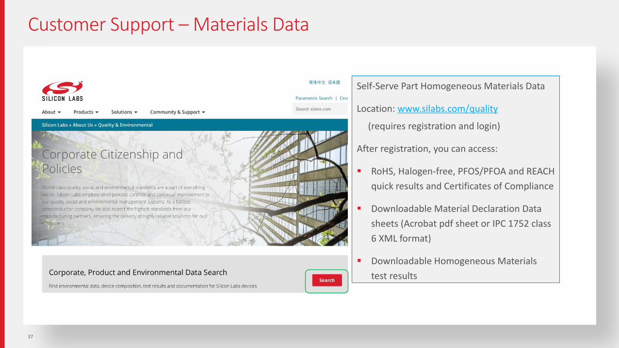
Customer Support – Materials Data
Self-Serve Part Homogeneous Materials Data
Location: www.silabs.com/quality
(requires registration and login)
After registration, you can access:
RoHS, Halogen-free, PFOS/PFOA and REACH
quick results and Certificates of Compliance
Downloadable Material Declaration Data
sheets (Acrobat pdf sheet or IPC 1752 class
6 XML format)
Downloadable Homogeneous Materials
test results
37
Several categories of frequently asked questions and answers can be found at www.silabs.com/qualityincluding:
Corporate (e.g. Governance, Locations, Financials)
Product (e.g. Qualification, Traceability, Reporting)
Environmental (e.g. Substance Database, Awards)
Quality (e.g. Failure Analysis, 8Ds, ISO Registrations)
Operations (e.g. Logistics, Supplier Management, Ordering)
Customer Support – FAQs
38
Thank you!S I L A B S . C O M