Embed Size (px)
Citation preview

JOURNAL OF LIGHTWAVE TECHNOLOGY, VOL. 14, NO. 5, MAY 1996 873
Silicon-Based Polarization Optics for the 1.30 and 1.55 pm Communication Wavelengths
R. M. A. Azzam and M. M. K. Howlader
Abstract-A modular three-reflection prism of Si can be de- signed to function as an in-line (nondeviating) linear polarizer or quarterwave retarder at the 1.30 and 1.55 pm lightwave communication wavelengths. Si-related thin films are employed as optical coatings. In particular, a single-layer antireflection coating of Si3N4 is used at the entrance and exit faces, and a Si02 film controls the polarization and total internal reflection phase shifts at the side surfaces of the prism. The angular and wavelength sensitivity of these proposed Si-based polarization optical elements is also considered.
I. INTRODUCTION ONTROL and measurement of the state of polarization C (SOP) of light is of considerable practical importance
in optics and lightwave technology. A basic set of optical elements that is often used to generate an arbitrary SOP, corresponding to any point on the surface of the Poincare sphere, consists of a linear polarizer P and a quarter-wave retarder (QWR) [l]. These elements are placed in the path of a collimated light beam (from a source L) and are rotated around its axis as a common axis, Fig. l(a). To change the SOP of the emergent beam without changing its power, light from the source L should be unpolarized or partially or totally circularly polarized. If the direction in which light traverses these two elements is reversed and a photodetector D is added to intercept the emergent radiation, Fig. l(b), the same system can function as a complete polarization analyzer or photopolarimeter [2]. The dual arrangements shown in Fig. l(a) and (b) are sometimes referred to as a polarization state generator (PSG) and a polarization state detector (PSD) [3], respectively. In a fiber-optic sensor or communication system, a PSG is used to launch light of known SOP at the input end of the fiber and a PSD is used to detect the received SOP at the output end.
Current polarization optics technology is based on double refraction and transmission in birefringent crystals (mainly cal- cite and quartz), or on reflection at coated or uncoated surfaces [4]. In this paper we describe modular linear polarizers and QWR s that are made of optically isotropic, 1R-transparent, Si for the 1.30 and 1.55 pm communication wavelengths [5]. The same prism design, Fig. 2, is used as an in-line three- reflection polarizer or QWR. Si-related thin films, namely Si02 or Si3N4, are applied to the entrance, exit, and side surfaces of the prism. Therefore, the same processes that are used in
Manuscript received July 11, 1994, revised February 15, 1996. The authors are with the Department of Electrical Engineering, University
Publisher Item Identifier S 0733-8724(96)03864-9. of New Orleans, New Orleans, LA 70148 USA.
L P QWR (a)
D P QWR (b)
Fig. 1. A linear polarizer P and a quarterwave retarder QWR are the essential components of a polarization state generator (a), and a polarization state detector, (b). L is a source of monochromatic collimated light and D is a photodetector.
r-------L 4 Fig. 2. Symmetrical three-reflection prism that can be used as an in-line polarizer or quarterwaver retarder by controlling the prism angle a. The figure is drawn for cy = 56.3' which corresponds to a Si polarizer at 1.55-pm wavelength.
integrated circuit technology may be employed to deposit these films on the prism faces to serve an optical function. The angular and wavelength sensitivity of these polarizing optical devices is considered.
11. GEOMETRICAL CONSIDERATIONS The symmetrical prism in Fig. 2 is specified by the prism
angle cy and axial length L. Ffrom geometry, and for a light beam that travels parallel to the base, the angles of incidence for internal reflection at the three side surfaces of the prism are
41 = a!, 4 2 = 2a -goo, 4 3 =: 41 = a!. (1)
0733-8724/96$05.00 0 1996 IEEE

Fig 3 Si prism mounted in a cylindrical sleeve for rotatlon around the incident light beam as an axis Here the pnsm is drawn for CY = 77.6O to correspond to a quarterwave retarder at the 1 30 and 155 p m wavelengths Note the smaller aspect rabo of the pnsm
The hight h of the beam axis (or center line) above the base of the prism is given by
h = (L/4) tan(180' - 201). (2)
The minimum "waist" w of the prism is determined by
w = h - ( L / 4 ) cot Q = (L/4)[tan(180° - 2a) - cot a]
(3)
and the maximum "aperature" or beam diameter A is
A = ( L / 2 ) cot a. (4)
An aspect ratio AR can be defined as the ratio of aperature to axial length
(5) AR = A / L = 0.5 cot a.
Because of the odd number of reflections that are used to steer the beam, there is a mirrorlike inversion of the beam cross section with respect to the central plane at hight h above the base. Also, if the incident beam is not exactly parallel to the base, the direction of the emergent beam will deviate from that of the incident beam by double the input angular deviation. The prism can be mounted in a rotatable cylindrical sleeve (tube) whose axis is the light beam center line, Fig. 3; the tube, in turn, can be mounted in the hollow shaft of a stepping motor for rotation control, or in a concentric graduated circle for accurate azimuth reading.
111. SILICON POLARIZERS Polarization takes place by Brewster-angle internal reflec-
tion at the base of the Si prism. The first and third internal reflections are total reflections that serve to bring the beam back in line. In the absence of a Si02 film, the essential characteristics of the prism polarizer can be readily calculated and are listed in Table I. This includes the prism angle a, the polarizing angle at the base 42, and the throughput or power transmittance for the unextinguished s polarization E,. The refractive indexes of Si at the 1.30 and 1.55 pm wavelengths are calculated from a dispersion relation given in [6]. For completeness, we also give the internal differential reflection phase shifts A, and A2 at the side surfaces of the prism in Table I.
A2 1 90" is consistent with the fact that the polarizing angle coincides with the principal angle in the limit of zero absorprtion in Si [7].
The light beam radiated out of the base of the prism can be dumped, or it may serve a useful function, such as providing a reference signal.
JOURNAL OF LIGHTWAVE TECHNOLOGY, VOL 14, NO 5, MAY 1996
TABLE I PRISM POLAFSZERS BASED ON BREWSTER-ANGLE INTERNAL REFLECTION AT THE Si-AR INTERFACE*
U r n ) 14i a=@,(") O f ( ? AI(") A , ( " ) % ( a )
1.30 3.5053 52.9613 15.9225 70.3504 90.000 72.16
1.55 3.4777 53.0212 16.0424 70.1765 90.000 71.79
*No Si02 film i s assumed to be present X is the vacuum wavelength of light and nSz is the refractive index of SI calculated from [6] a is the prism angle, and dl and 42 are angles of incidence for internal reflection at the side surfaces of the prism (see Fig 2) A1 and A2 are the associa differenbal internal reflecaon phase shifts at 41 and 42, Rs is the throughput for the transmtted 5 polarization
-90 , I I I I , I I 1 I I , , , , , n r i I / # I / I , I I I I , I # / I n , I I I I I , , I \ , I I ,
m r ? ~ * m o m m r . r . w
x
-90 o ~ o o o m o m o ~ o - - - - - - - - - - -
Fig. 4. Extinction ratio ER (dB) as a function of wavelength X for the two Si polarizer designs listed in Table I Polarization takes place by internal reflection at the Si-air interface at the Brewster angle
Fig. 4 shows the extinction ratio ER in dB, which is defined by
ER = 10 log,o(Rp/R,) (6)
as a function of wavelength X in the 1.30-1.80 pm spectral range for each of the two polarizer designs given in Table I. It is evident that polarization can be efficiently obtained at both the 1.30 and 1.55 pm wavelengths simultaneously using any one of the two prisms. If the, prism angle Q is rounded off to 53", such a prism would function as an excellent polarizer with ER= - 28.89 and -34.95 dB at wavelengths of 1.30 and 1.55 pm, respectively.
Fig. 5 shows the ER as a function of a small angle-of- inzidence error at the entrance face, within +lo of normal incidence. This figure illustrates the limited field of view af the Si polarizer and gives an estimate of the degree of collimation that is required of the incident beam for excellent polarization.
The assumption of a bare Si surface can be realized in practice only by preventing the oxidation of Si. This requires that the space between the side surfaces of the prism and the sleeve in which it is mounted (Fig. 3) be evacuated or filled with an inert gas and sealed. However, this procedure may not be required. This is because a natural Si02 film of -10

AZZAM AND HOWLADER: SILICON-BASED POLARIZATION OPTICS 875
Fig. 5. the entrance face of the Si prism polarizers listed in Table I.
Extinction ratio ER (dB) as a function of the angle of incidence 0 at
-1.41
-1.42
-1.43
-1.44
-1.45 %(a) -1.46
-1.47
-1.48
-1.49
-1.50
d (~1 )
Fig. 7. Throughput R, (dB) for the unextinguished s polarization as a function of the thickness d of an Si02 film at the base of the Si prism polarizers of Table I.
Fig. 6. Extinction ratio ER (dB) as a function of the thickness d of an Si02 x film at the base of the Si prism polarizers of Table I. Fig. 8. Extinction ratio ER (dB) as a function of wa-velength X for the two
polarizer designs of Table I when an absentee layer of Si02 is added at the base. Note that each polarizer is useable only at or in the immediate vicinity of its own design wavelength. nm thickness, which effectively prevents the further oxidation
of Si [8], has a small effect on the ER. This is illustrated in Fig. 6 which shows the ER as a function of the thickness d of the oxide film in the 0-50 nm range. For completeness, Fig. 7 shows the throughput or insertion loss R, also as a function of d. The insertion loss of the device for the transmitted s polarization is low (<1.5 dB).
Another interesting possibility is to coat the base of the prism, where polarization takes place, by a so-called “absentee layer” [9] of Si02 whose thiclcness is equal to one period,
on small deviations of the absentee layer thickness from the exact value given by (7).
Fig. 8 shows the dispersion of the ER aver the 1.30-1.80 pm spectral range. Because of the greater thickness of the absentee layer, a polarizing prism designed for one of the two communication wavelengths cannot be used as a polarizer at the other wavelength. The oxide film thickness on the V- shaped side surfaces is not critical in this application (as it
ci = D# = ( ~ / 2 > ( N ; - N; sin2 +2)-1’2 (7)
where X is the vacuum wavelength of light and No and NI are the refractive indexes of Si and Sios, respectively. From the known dispersion of Si and SiiOz [6], we calculate d = 601.0 and 718.8 nm at X = 1.30 and 1.55 pm, respectively. Figs. 6 and 7 now give the dependence of the ER and R,, respectively,
only affects the total internal reflection phase shifts), and may be equal to that of the film at the prism base.
It is also possible to make the polarizing reflection entirely insensitive to the Si02 film thickness. This i!j done by optically cementing the oxidized Si prism at its base to a thick slab of fused quartz (silica) using an index-matching glue, as shown in Fig. 9. (The second or outer surface of the silica slab may

876
/.......... . . . . . . . . . . . . . . . . . . . . . . . . . . . . . . I . . . . . . . . . . . . . . . . . . . . . . . . . . . . . . . . 1 I .I . . . . . . . .'.Bulk. - . - S i . O ~ - . - . - . ~ . ~ . ~ . ~ . ~ . ~ . . . . . . . . . .
. . . . . . . . . . . . . . . . . . . . . . . . . . . . . . . . . . . . . . . . . . . . . . . . . . . . . . . . . . . . . . . .
Fig. 9. Prism polarizer using Brewster-angle reflection at an embedded Si-SiOZ interface. A fused-quartz (silica) slab is cemented to the oxidized base of the Si prism using an index-matching glue.
be roughened and blackened to absorb the refracted beam and to prevent unwanted multiple reflections from leaking out.) In this device polarization takes place at the Brewster angle of the embedded Si-Si02 interface (prism angle Q = 56.217 and 56.277" and 4 2 = 22.433 and 22.554" at 1.30 and 1.55 pm, respectively) and the device throughput for the transmitted s polarization is decreased to 50% (3 dB insertion loss). Because thin-film interference has been removed, the device becomes more achromatic.
To our knowledge, a prism polarizer of the type described here is new. However, an in-line IR polarizer that uses a Si surface and two A1 mirrors in external reflection is known [lo].
IV. SILICON QUARTERWAVE RETARDERS A prism of the same construction shown in Fig. 2 is used.
However, a larger prism angle 01 is necessary to guarantee total internal reflection at all three side surfaces of the prism and to ensure that the net accumulated differential reflection phase shift A, after three reflections is equal to the desired 90". For simplicity, we assume that the Si02 film thickness d is the same on all three side surfaces of the prism.
Fig. 10 shows A, as a function of 01 in a narrow range of 1" (77.3 to 78.3") for different values of d from 0 to 150 nm in steps of 25 nm, and also for d = 200 and 500 nm, which correspond to the bottom two lines. These results are calculated at a wavelength of 1.55 pm.
The constraint between a and d such that A, = 90° at X = 1.55 pm is represented in Fig. 11 and corresponds to the points of intersection of the A, = 90" straight line with the family of curves in Fig. 10. Also shown in Fig. 11 is the corresponding curve for the 1.30 pm wavelength. The saturation that sets in for d 2 500 nm represents a desirable feature. It indicates that a Si02 film thickness 2500 nm is well above the penetration depth of the evanescent wave field associated with total reflection at the Si-Si02 interface. A choice of film thickness in that range makes A, insensitive to film thickness errors and to any externally adsorbed layers, so that an environmentally stable device is obtained. It also makes the QWR more achromatic.
JOURNAL OF LIGHTWAVE TECHNOLOGY, VOL. 14, NO 5, MAY 1996
84 r ? % m a r . m c n o - ~ n r . h r . h b r . b m m m m r - r . r . r . r . r . r . r . r . r . r .
a
Fig. 10. Net differential reflection phase shift &,at X = 1 55 p,m as a function of the pnsm angle cy for different values of the thickness d of an Si02 film from 0 to 150 nm in steps of 25 nm The bottom two curves are for d = 200 and 500 nm. d is the same for the S i 0 2 film on all three side surfaces of the Si pnsm.
78.3
78.2 178 2
78.1
78.0
77.9
a 77.8
77.7
7 7 6 h,F177.6 77.5 77.5
4 L
77.4 ~ ~ 7 7 . 4 D 0 0 0 0 0 0 0 0 0 0
0 0 0 0 0 0 0 0 0 0 - c 4 m - k l n w r . m c n
d (4 z Fig 11. that A, = 90' (i.e., QWR) at 1.30 and 1.55 p,m wavelengths
Constrant on the pnsm angle cy and S i 0 2 film thickness d such
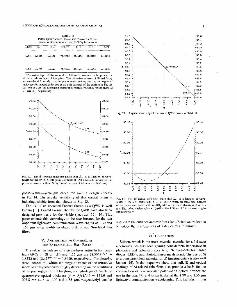
Table I1 summarizes the calculated data for two Si-prism QWR's at 1.30 and 1.55 pm using an optically thick oxide film (d = 500 nm). Because of the relatively small dispersion of the materials, the prisms are almost identichl. As shown in Fig. 12, either prism can be used as a QWR with a very small phase error (<0.2') over the extended 1.30-1.80 pm spectral range. Fig. 13 indicates reasonable angular sensitivity (< 1.6" phase error per 1" incidence angle error), so that acceptable performance is obtained without a stringent limitation on the collimation of the input beam.
It is possible (at least theoretically) to deSign one prism that would produce nearly exact QWR at the 1.30 and 1.55 pm simultaneously. Such a design uses a prism angle Q = 77.5884" and an oxide thickness d = 155 nm. The net
AZZAM AND HOWLADER SILICON-BASED POLARIZATION OPTICS 871
TABLE I1
INTERNAL REFLECTION Air THE Si-Si02 INTERFACE*
h t r m ) nsi kO2 a=01(") AI(") A,(")
PRISM QUARTERWAVE RECARDERS BASED ON TOTAL
1.30 3.5053 1 .4472 77 .5736 65.1472 22 ,5855 44.8290
1 .55 3 .4777 1 .4444 77 .5566 65.1132 22.5874 44.8252
*An oxide layer of thickness d =I 500nm is assumed to be present on all three side surfaces of the prism. The refractive indexes of Si and Si02 are calculated from [6] . cy is the prism angle, and 41 and 4 2 are angles of incidence for internal reflection at the side surfaces of the prism (see Fig. 2). A1 and A2 are the associated differential internal reflection phase shifts at 41 and 4 2 , respectively.
90.12 ,
90.08 F 190.04
89.96
89.92 89.92
89.88 89.88
! \ 1.30
Fig. 12. Net differential reflection phase shift A, as a function of wave- length for the two Si QWR prisms of Table 11. (All three side surfaces of the prism are coated with an Si02 film of the same thickness d = 500 nm.)
phase-versus-wavelength cunre for such a design appears in Fig. 14. The angular sensitivity of this special prism is indistinguishable from that shown in Fig. 13.
The use of an uncoated Fresnel rhomb as a QWR is well known [ 111. Coated Fresnel rhombs for QWR have also been designed previously for the visible spectrum [ 1214 141. This paper extends this technology to the near infrared for the two important lightwave communication wavelengths of 1.30 and 1.55 pm using readily available bulk Si and Si-related thin films.
v. ANTIREFLECITON COATINGS AT THE ENTRANCE AND EXIT FACES
The refractive indexes of a single-layer antireflection coat- ing (ARC) on Si at 1.30 and 1.55 pm are (3.5053)lI' = 1.8722 and (3.4777)l/' = 1.8649, respectively. Fortuitously, these indexes fall within the range of values of the refractive index of nonstoichiometric Si2,N4 depending on the conditions of its preparation [15]. Therefore, a single-layer of Si3N4 of quarterwave optical thickness [d = X/(4N1) = 173.6 and 207.8 nm at X = 1.30 and 1.55 pm, respectively] can be
-91.6
-90.8
-89.6
Fig. 13. Angular sensitivity of the two Si QWR prisms of Table 11.
90.10
90.08
90 06
Aa 90.04
90.02
90.00
89.98
Fig. 14. Net differential reflection phase shift A, as a function of wave- length X for a Si prism with cy = 77.5884O when all three side surfaces of the prism are coated with an Si02 film of the same thickness d = 155 nm. This prism design achieves QWR at the 1.30 and 1.55 pm wavelengths simultaneously.
applied to the entrance and exit faces for efficient antireflection to reduce the insertion loss of a device to ii minimum.
VI. CONCLUSION Silicon, which is the most essential material for solid state
electronics, has also been gaining considerable importance in photonics and optoelectronics (e.g., Si photodetectors, laser diodes, LED's, and photoluminescent devices). The use of Si as a transparent lens material for IR imaging optics is also well known [16]. In this paper we show that bulk Si and optical coatings of Si-related thin films also provide a basis for the construction of new modular polarization optical devices for use in the near IR, and in particular at the 1.30 and 1.55 pm lightwave communication wavelengths. This includes in-line

878 JOURNAL OF LIGHTWAVE TECHNOLOGY, VOL 14, NO 5, MAY 1996
linear polarizers and quarterwave retarders whose angular and wavelength sensitivity is also considered.
REFERENCES , [I] R. M. A. Azzam and N. M. Bashara, Ellipsometry and Polarized Lighf.
Amsterdam: North-Holland, 1987. [2] D. Clarke and J. F. Grainger, Polarized Light and Optical Measurement.
New York: Pergamon, 1971. [3] P. S. Hauge, “Recent developments in insmimentation in ellipsometry,”
Surjace Sci., vol. 96, 1980, pp. 108-140 [4] J. M. Bennett and H. E. Bennett, “Polarization,” Section 10 in Handbook
ofOptics, W. G. Driscoll and W. Vaughan, Eds., New York McGraw- Hill, 1978.
[5] B. E. A. Saleh and M. C. Teich, Fundamentals of Photonics. New York: Wiley, 1991.
[6] M. Herzberger and C. D. Salzberg, “Refractive indices of infrared optical materials and color correction of infrared lenses,” J. Opt. Soc. Am., vol. 52, pp. 420-427, Apr. 1962.
[7] R. M. A. Azzam, “Contours of constant principal angle and constant principal azimuth in the complex E plane,” J. Opt. Soc. Am., vol. 71, pp. 1523-1528, Dec. 1981.
[SI R. J. Archer, “Optical measurement of film growth on silicon and germanium surfaces in! room air,” J. Electrochem. Soc., vol. 104, pp. 619-622, Oct. 1957. ,
[9] Z. Knittl, Optics of Thin Films. [lo] R. T. Baume1 and S.: E. Schnatterl), “Silicon reflection polarizer for the
infrared,” J. Opt. Soc. Am., vol. 61, pp. 832-833, June 1971. [ll] M. Born and E. Wolf, Principles of Optics, 5th Edition, New York
Pergamon, 1975, pp. 47-51. 1121 P. B. Clapham, M. J. Downs, and R. J. King, “Some applications of thin
films to polarization devices,” Appl. Opt., vol. 8, pp. 1965-1974, 1969. [13] J. M. Bennett, “A critical evaluation of rhomb-type quarterwave re-
tarders,” Appl. Opt., vol. 9, pp. 2123-2129, Sept. 1970. [14] R. P. Netterfield, P. J. Martin, W. G. Sainty, R. M. Duffy, and C. G.
Pacey, “Characterization of growing thin films by in-situ ellipsometry, spectral reflectance and transmittance measurements, and ion-scattering spectroscopy,” Rev. Sci. Instrum., vol. 56, pp. 1995-2003, Nov. 1985.
[15] G. Eisenstein and L. W. Stulz, <‘High quality antireflection coatings on’laser facets by sputtered silicon nitride,” Appl. Opt., vol. 23, pp. 161-164, Jan., 1984.
New York: Wiley, 1976.
[16] The InfraredHandbook, W L Wolfe and G J Zissis, Eds , MI Environmental Research Institute, 1978.
Ann Arbor,
R. M. A. Azzam received the B Sc degree froin Calro University, Egypt m 1967, and the Ph D degree from the University of Nebraska-Lincoln in 197 1, both in electncal engineenng
He is currently a Distinguished Professor of electrical engineering at the University of New Orleans He is also the Polarization Optics Topical Edtor for Applied Oprics (Optical Technology Division) and was the Topical E&tor for “Polanzation and Thm Films” €or the Journal of the Optzcal Society of America A from 1985 to 1989 He was also Guest Co-editor of special issues of Surface Science, Optical Engineering, and the Journal of the Optical Society ofAmerica A, and editor of the SPIE Milestone Series volume, Selected Papers on Ellipsometry, published in 1991 Azzam was a Fulbnght senior research scholar in France from 1985 to 1986 He has four patents and is author or co-author of over 200 journal papers and the monograph, Ellipsometry and Polarized Light, which was first published by North-Holland in 1977, translated into Russian by Mir, Moscow, 1981, and appeared in paperback in 1987.
Dr Azzam is a Fellow of the Optical Society of America and The Internahonal Society for Optical Engineering (SPIE) He was recognized as an outstanding American Inventor and placed as a finalist in the cornpention for the Amenca’s 1988 Inventor of the Year Award, sponsored by Intellectual Property Owners, Inc , for h s four-detector photopolarimeter, which lead to the commercial development of the STOKESMETER by Gaertner. He received a Photonics Clrcle of Excellence Award and in 1993 won the R&D 1 0 0 Award for ths invention
M. M. K. Howlader received the B Sc degree in electrical engiueering from Bangladesh University of Engineering and Technology in 1991, and the M Sc in electncal engineenng from the University of New Orleans in 1994 He is currently pursuing the Ph D degree in electrical engineerink at the University of Central Flonda.
He is a student member of the Optical Society of America In 1994 he received a graduate fellowship at the Center foi Research and Education in Optics and Lasers (CREOL)
,
,
![IEEE JOURNAL OF SELECTED TOPICS IN QUANTUM … · electron concentrations higher than 1018 cm−3 at a wavelength of 1.55 μm (see Fig. 1). Experimental data from [7] shows reasonable](https://img.pdfslide.us/doc/110x75/5ea0ae5dbf66fd59d51ce9ff/ieee-journal-of-selected-topics-in-quantum-electron-concentrations-higher-than-1018.jpg)