Embed Size (px)
Citation preview

Applications Note: SY5019 Flyback controller
For adapters or chargers
AN_SY5019 Rev.0.9B Silergy Corp. Confidential- Prepared for Customer Use Only 1
General Description
SY5019 is a PWM/PFM controller with several features
to enhance performance of Flyback converters that
targeting at adapter or charger applications. It drives
Flyback controller in the Quasi-Resonant mode for
higher efficiency and better EMI performance. SY5019
adopt burst mode control for improved efficiency and
the output current is detected by internal primary
detection technology to achieve more reliable Over
Current Protection and Short Circuit Protection. The
output voltage is achieved by secondary side control
technology for good load and line regulation. SY5019
provides a fast internal HV start up circuit without
consuming any standby power to achieve lowest no-load
power consumption.
Ordering Information
Package Code
Temperature Code
Optional Spec Code
()SY5019
Features
• Quasi-Resonant (QR) mode operation: Valley turn-
on of the primary MOSFET to achieve low
switching losses
• Output current is monitored by primary detection for
reliable Over Current Protection and Short Circuit
Protection
• PWM/PFM control for higher average efficiency
• Burst mode control for low no load loss and
efficiency
• HV start up circuit is used to reduce no-load.
• Internal high current MOSFET driver: 120mA
• Auto-Recovery for OVP/OCP/SCP/OTP
• Maximum frequency limitation 125kHz
• Compact package: SO8
Applications
• AC/DC Adapters
• Battery Chargers
• Consumer Electronics
• Auxiliary power supplies
Typical Applications
Fig.1 Schematic Diagram
Ordering Number Package type Note
SY5019FAC SO8 ----
Silerg
y Cor
p. Con
fiden
tial-P
repare
d for
PST

AN_SY5019
AN_SY5019 Rev.0.9B Silergy Corp. Confidential- Prepared for Customer Use Only 2
Pinout (top view)
(SO8)
Top Mark: BAExyz (device code: BAE, x=year code, y=week code, z= lot number code)
Pin Name Description
1 GND Ground pin.
2 DRV Gate driver pin. Connect this pin to the gate of primary MOSFET.
3 NC Not Connect
4 HV Connect an internal HV start up circuit. Connect this pin to Bus or Drain Pin of Primary MOSFET.
5 VIN Power supply pin.
6 VSEN Inductor current zero-crossing detection pin. This pin receives the auxiliary winding voltage by a
resistor divider and detects the inductor current zero crossing point.
7 COMP Feedback input pin. The PWM ducy cycle is determined by voltage level into this pin.It’s connected to a
optocoupler.
8 ISEN Current sense pin. Connect this pin to the source of the primary switch.
Block Diagram
+-
VIN
Bias Supply
VCCLogic
VREF
IREF
VIN_OK
VIN_OVP
VSEN
VOUTDetection
Cable Comp.
VVSEN_OVP
VVSEN_FB
ISEN IPK_SEN
IOUT_SEN
CO
MP
PWMGenerator
COMP
COMP Behavior(Frequency_ set、Ipk_set、
Fast Transient Response )
VSEN
IPK_SET
Flimit_SET
DRIVERPWM DRV
IOUT_SEN
Protection
VIN_OVP
VVSEN_OVP
IPK_SEN
Hiccup
GN
D
VREF OCP
2.5V
IOUTCalculator
20k
HV HV Start up
circuit
Fig.2 Block Diagram
Silerg
y Cor
p. Con
fiden
tial-P
repare
d for
PST

AN_SY5019
AN_SY5019 Rev.0.9B Silergy Corp. Confidential- Prepared for Customer Use Only 3
Absolute Maximum Ratings (Note 1) HV------------------------------------------------------------------------------------------------------------------------------------ 600V
VIN---------------------------------------------------------------------------------------------------------------------------- -0.3V~21V
Supply Current IVIN-----------------------------------------------------------------------------------------------------------------20mA
VSEN ----------------------------------------------------------------------------------------------------------------- -0.3V~VVIN+0.3V
DRV ------------------------------------------------------------------------------------------------------------------------- -0.3V~15V
ISEN, COMP ----------------------------------------------------------------------------------------------------------- -0.3V~3.6V
Power Dissipation, @ TA = 25°C SO8 ----------------------------------------------------------------------------------------- 1.1W
Package Thermal Resistance (Note 2)
SO8,θJA----------------------------------------------------------------------------------------------------------------------125°C/W
SO8, θJC----------------------------------------------------------------------------------------------------------------------60°C/W
Junction Temperature Range ----------------------------------------------------------------------------------------- -45°C to 150°C
Lead Temperature (Soldering, 10 sec.) ---------------------------------------------------------------------------------------- 260°C
Storage Temperature Range ------------------------------------------------------------------------------------------ -65°C to 150°C
Recommended Operating Conditions (Note 3) VIN -------------------------------------------------------------------------------------------------------------------------- 9V~17.5V
Junction Temperature Range ----------------------------------------------------------------------------------------- -40°C to 125°C
Ambient Temperature Range ---------------------------------------------------------------------------------------- -40°C to 105°C
Silerg
y Cor
p. Con
fiden
tial-P
repare
d for
PST

AN_SY5019
AN_SY5019 Rev.0.9B Silergy Corp. Confidential- Prepared for Customer Use Only 4
Electrical Characteristics (VIN = 12V, TA = 25°C unless otherwise specified)
Parameter Symbol Test Conditions Min Typ Max Unit
Power Supply Section
Input voltage range VVIN 9 17.5 V
VIN turn-on threshold VVIN_ON 13.7 14.7 15.7 V
VIN turn-off threshold VVIN_OFF 6.3 7 8.3 V
VIN OVP voltage VVIN_OVP 17.5 18.5 19.5 V
HV start up current IHV_ON 1.5 mA
HV leakage current IHV_OFF VHV=373V 3 µA
Start up current IST VVIN<VVIN_OFF 1.2 4 µA
Operating current IVIN CL=100pF,f=100kHz 1.5 mA
Quiescent current IQ 100 300 600 µA
Shunt current in OVP mode IVIN_OVP VVIN>VVIN_OVP 9 mA
Current Feedback Modulator Section
Internal reference voltage VREFI 0.413 0.42 0.426 V
ISEN Pin Section
Current limit voltage VISEN_LIM VFBV<0.4V 0.7 V
VFBV>0.4V 0.9 1 1.1 V
Latch voltage for ISEN VISEN_EX 2 V
CC feedforward resistor Rk2 225 300 375 Ω
VSEN Pin Section
OVP voltage threshold VVSEN_OVP 1.37 1.45 1.52 V
COMP Section
Internal voltage bias VCVB 2.5 V
Sleep mode voltage ON threshold VCOMP_ON 0.4 V
Sleep mode voltage OFF threshold VCOMP_OFF 0.45 V
Internal pull-up resistor RCOMP 20 kΩ
Gate Driver Section
Gate driver voltage VGATE 12 V
Maximum. source current ISOURCE_MAX 120 mA
Maximum. sink current ISINK_MAX 500 mA
Max ON Time TON_MAX VCOMP=2.5V 24 µs
Min ON Time TON_MIN 100 300 400 ns
Max OFF Time TOFF_MAX 400 500 650 µs
Min OFF Time TOFF_MIN 1.2 µs
Minimum switching period TPERIOD_MIN 7 8 9 µs
Thermal Section
Thermal shutdown temperature TSD 150 °C
Note 1: Stresses beyond the “Absolute Maximum Ratings” may cause permanent damage to the device. These are stress
ratings only. Functional operation of the device at these or any other conditions beyond those indicated in the
operational sections of the specification is not implied. Exposure to absolute maximum rating conditions for extended
periods may affect device reliability.
Note 2: θJA is measured in the natural convection at TA = 25°C on a low effective single layer thermal conductivity test
board of JEDEC 51-3 thermal measurement standard. Test condition: Device mounted on 2” x 2” FR-4 substrate PCB,
2oz copper, with minimum recommended pad on top layer and thermal vias to bottom layer ground plane.
Note 3: Increase VIN pin voltage gradually higher than VVIN_ON voltage then turn down to 12V.
Silerg
y Cor
p. Con
fiden
tial-P
repare
d for
PST

AN_SY5019
AN_SY5019 Rev.0.9B Silergy Corp. Confidential- Prepared for Customer Use Only 5
Operation
SY5019 is a PWM/PFM controller with several features
to enhance performance of Flyback converters.
To achieve higher efficiency and better EMI performance,
SY5019 drives Flyback converters in the Quasi-Resonant
mode; the start up current of the device is rather
small(4µA max) to reduce the standby power loss further
and the maximum switching frequency is limited below
125kHz.
In order to improve the stability, the self-adaption
compensation is applied.
The output current is monitored by primary side detection
technology, and the maximum output current can be
programmed in Over Current Protection and Short Circuit
Protection. In addition to SY5019 provides Over Voltage
Protection (OVP), Over Temperature Protection (OTP),
VSEN pin short protection, etc..
SY5019 can be applied in AC/DC adapters, Battery
Chargers and other consumer electronics.
SY5019 is available with SO8package.
Applications Information
Start up
After AC supply or DC BUS is powered on, the capacitor
CVIN across VIN and GND pin is charged up by BUS
voltage through HV start up circuit. Once VVIN rises up to
VVIN_ON, the internal blocks start to work. VVIN will be
pulled down by internal consumption of IC until the
auxiliary winding of Flyback transformer could supply
enough energy to maintain VVIN above VVIN_OFF.
The whole start up procedure is divided into two sections
shown in Fig.3. tSTC is the CVIN charged up section, and
tSTO is the output voltage built-up section. The start up
time tST composes of tSTC and tSTO, and usually tSTO is
much smaller than tSTC.
Fig.3 Start up The CVIN are designed by rules below:
(a) Select CVIN to obtain an ideal start up time tST, and
ensure the output voltage is built up at one time.
HV_ON ST HV_OFF ST
VIN
VIN_ON
(I I I ) tC =
V
− − × (1)
(b) If the CVIN is not big enough to build up the output
voltage at one time. Increase CVIN until the ideal start up
procedure is obtained.
Shut down
After AC supply or DC BUS is powered off, the energy
stored in the BUS capacitor will be discharged. When
the auxiliary winding of Flyback transformer cannot
supply enough energy to VIN pin, VVIN will drop down.
Once VVIN is below VVIN_OFF, the IC will stop working.
Quasi-Resonant Operation(valley detection)
QR mode operation provides low turn-on switching
losses for Flyback converter.
Fig.4 QR mode operation
The voltage across drain and source of the primary
MOSFET is reflected by the auxiliary winding of the
Silerg
y Cor
p. Con
fiden
tial-P
repare
d for
PST

AN_SY5019
AN_SY5019 Rev.0.9B Silergy Corp. Confidential- Prepared for Customer Use Only 6
Flyback transformer. ZCS pin detects the voltage across
the auxiliary winding by a resistor divider. When the
voltage on VSEN pin across zero, the MOSFET would be
turned on after 400ns delay.
Output Voltage Control(CV control )
SY5019 is compatible with opto-coupler to achieve
output voltage control, which is shown by Fig.5.
COMP
+-
VOUT
2.5V
20k
GND
SY5019
VCVB
RCOMP
IOPT_OUT RFBU
RFBD
ROPTIOPT_IN
Fig.5 Output voltage feedback circuit
The OFF time of MOSFET is up to the valley detection
of VSEN pin, and the ON time of MOSFET is a function
of VCOMP, so the output power can be controlled by
VCOMP.
SY5019 integrates an internal 2.5V voltage bias and
20kΩ resistor to interface the output of opto-coupler.
VCOMP is in relation with the output current of the opto-
coupler IOPT_OUT by
COMP CVB OPT _ OUT COMPV V I R= − × (2)
ROPT is the resistor across the output node and the anode
of the opto-coupler. The selection of ROPT is related with
system loop stability, and higher loop gain of the system
is achieved by smaller ROPT.
At the same time, ROPT is designed by
CVB OPT _ IN _ MAX COMP COMP _ ONV I R V− ×β× < (3)
Where β is the transfer ratio of the opto-coupler;
IOPT_IN_MAX is the maximum input current through the
opto-coupler, which is limited by ROPT.
Output current detection by Primary side(CC control)
The output current is monitored by SY5019 with primary
side detection technology. The maximum output current
IOUT_LIM can be regulated by:
1 2 REF PS
OUT_LIM
S
k k V NI =
R
× × × (4)
Where k1 is the output current weight coefficient; k2 is
the output modification coefficient; VREF is the internal
reference voltage; NPS is the turns ratio of the Flyback
transformer; RS is the current sense resistor.
k1 , k2 and VREF are all internal constant parameters,
IOUT_LIM can be programmed by NPS and RS.
1 2 REF PS
S
OUT_LIM
k k V NR =
I
× × × (5)
When over current operation or short circuit operation
happens. VCOMP will be pulled down, and the output
current will be limited at IOUT_LIM. The V-I curve is
shown as Fig.6.
Fig.6 V-I curve
Line regulation modification
The IC provides line regulation modification function to
improve line regulation performance of the output
current.
Due to the sample delay of ISEN pin and other internal
delay, the output current increases with increasing input
BUS line voltage. A small compensation voltage
∆VISEN_C is added to ISEN pin during ON time to
improve such performance. This ∆VISEN_C is adjusted by
the upper resistor of the divider connected to VSEN pin.
AUX
ISEN_C BUS 3
P VSENU
N 1∆V =V k
N R× × × (6)
Where RVSENU is the upper resistor of the divider; k3 is
an internal constant as the modification coefficient.
Silerg
y Cor
p. Con
fiden
tial-P
repare
d for
PST

AN_SY5019
AN_SY5019 Rev.0.9B Silergy Corp. Confidential- Prepared for Customer Use Only 7
The compensation is mainly related with RVSENU, larger
compensation is achieved with smaller RVSENU. Normally,
RVSENU ranges from 50kΩ~150kΩ.
Short Circuit Protection (SCP)
There are two kinds of situations, one is the valley signal
cannot be detected by VSEN, the other is the valley
signal can be detected by VSEN.
When the output is shorted to ground, the output voltage
is clamped to zero. The voltage of the auxiliary winding
is proportional to the output winding, so valley signal
cannot be detected by VSEN. There are two cases,the
one is without valley detection, MOSFET cannot be
turned on until maximum off time is reached. If
MOSFET is turned on with maximum off-time for 64
times continuously which can not detected valley, IC will
be shut down and enter into hiccup mode. The other is
that IC will be shut down and enter into hiccup mode
when VVIN below VVIN_OFF within 64 times .
When the output voltage is not low enough to disable
valley detection in short condition, SY5019 will operate
in CC mode until VIN is below VIN_OFF.
In order to guarantee SCP function not effected by
voltage spike of auxiliary winding, a filter resistor RAUX
is needed.
Fig. 7 Filter resistor RAUX
Output voltage OVP protection
The secondary maximum voltage is limited by the
SY5019.When the VSEN pin signal exceeds 1.45V,
SY5019 will stop switching and discharge the VIN
voltage. Once VVIN is below VVIN_OFF, the IC will shut
down and be charged again by HV start up.
VSEN pin short protection
The SY5019 has a protection against faults caused by a
shorted VSEN pin or a shorted pull-down resistor. During
start-up, the voltage on the VSEN pin is monitored. In
normal situations, the voltage on the VSEN pin reaches
the sense protection trigger level. When the VSEN
voltage does not reach this level, the VSEN pin is
shorted and the protection is activated. The IC stops
switching and discharge the VIN voltage. Once VVIN is
below VVIN_OFF, the IC will shut down and be charged
again by HV start up. In order to ensure reliable
detection, the pull-down resistor should larger than 2kΩ.
Power Device Design
MOSFET and Diode
When the operation condition is with maximum input
voltage and full load, the voltage stress of MOSFET and
secondary power diode is maximized.
MOS_DS_MAX AC_MAX PS OUT D,F SV = 2V +N (V +V )+∆V× (7)
AC_MAX
D_R_MAX OUT
PS
2VV = +V
N (8)
Where VAC_MAX is maximum input AC RMS voltage;
NPS is the turns ratio of the Flyback transformer; VOUT is
the rated output voltage; VD_F is the forward voltage of
secondary power diode; ∆VS is the overshoot voltage
clamped by RCD snubber during OFF time.
When the operation condition is with minimum input
voltage and full load, the current stress of MOSFET and
power diode is maximized.
MOS_PK_MAX P_PK_MAXI =I (9)
MOS_RMS_MAX P_RMS_MAXI =I (10)
D_PK_MAX PS P_PK_MAXI =N I× (11)
D_AVG OUTI =I (12)
Where IP_PK_MAX and IP_RMS_MAX are maximum primary
peak current and RMS current, which will be introduced
later.
Transformer (NPS and LM)
NPS is limited by the electrical stress of the power
MOSFET:
MOS_(BR)DS AC_MAX S
PS
OUT D_F
V 90%- 2V -∆VN
V +V
×≤ (13)
Silerg
y Cor
p. Con
fiden
tial-P
repare
d for
PST

AN_SY5019
AN_SY5019 Rev.0.9B Silergy Corp. Confidential- Prepared for Customer Use Only 8
Where VMOS_(BR)DS is the breakdown voltage of the power
MOSFET; VAC_MAX is maximum input AC RMS voltage.
In Quasi-Resonant mode, each switching period cycle tS
consists of three parts: current rising time t1, current
falling time t2 and quasi-resonant time t3 shown in Fig.8.
VDS
IPRI
VG
ISEC
IOUT
t2t1tS
IPP
ISP
t3
Fig.8 Switching waveforms
When the operation condition is with minimum input AC
RMS voltage and full load, the switching frequency is
minimum frequency, the maximum peak current through
MOSFET and the transformer happens.
Once the minimum frequency fS_MIN is set, the inductance
of the transformer could be induced. The design flow is
shown as below:
(a)Select NPS;
MOS_(BR)DS AC_MAX S
PS
OUT D_F
V 90%- 2V -∆VN
V +V
×≤ (14)
(b) Preset minimum frequency fS_MIN ;
(c) Compute inductor LM and maximum primary peak
current I_PK_MAX ;
OUT OUTP _ PK _ MAX
DC _ MIN PS OUT D _ F
OUTDrain S_ MIN
2P 2PI
V N (V V )
2PC f
= +η× η× × +
+π × ×η
(15)
OUT
M 2
P _ PK _ MAX S_ MIN
2PL
I f=
η× × (16)
Where CDrain is the parasitic capacitance at drain of
MOSFET; η is the efficiency; POUT is rated full load
power; VDC_MIN is minimum input DC RMS voltage.
(d) Compute current rising time t1 and current falling
time t2;
M P_PK_MAX
1
DC_MIN
L It =
V
× (17)
M P_PK
2
PS OUT D_F
L It =
N (V +V )
××
(18)
S
S_MIN
1t =
f (19)
(e) Compute primary maximum RMS current IP_RMS_MAX
for the transformer fabrication ;
1
P_RMS_MAX P_PK_MAX
S
t3I = I
3 t (20)
(f) Compute secondary maximum peak current IS_PK_MAX
and RMS current IS_RMS_MAX for the transformer
fabrication .
S_PK_MAX PS P_PK_MAXI =N I× (21)
2
S_RMS_MAX PS P_PK_MAX
S
t3I = N I
3 t× × (22)
Transformer design (NP , NS , NAUX)
The design of the transformer is similar with ordinary
Flyback transformer.The parameters below are necessary:
Necessary parameters
Turns ratio NPS
Inductance LM
Primary maximum current IP_PK_MAX
Primary maximum RMS current IP_RMS_MAX
Secondary maximum RMS current IS_RMS_MAX
The design rules are as followed:
(a) Select the magnetic core style, identify the effective
area Ae ;
(b) Preset the maximum magnetic flux ∆B ;
∆B=0.22~0.26T
(c) Compute primary turn NP ;
Silerg
y Cor
p. Con
fiden
tial-P
repare
d for
PST

AN_SY5019
AN_SY5019 Rev.0.9B Silergy Corp. Confidential- Prepared for Customer Use Only 9
M P_PK_MAX
P
e
L IN =
∆B A
××
(23)
(d) Compute secondary turn NS ;
PS
PS
NN =
N (24)
(e) compute auxiliary turn NAUX ;
VIN
AUX S
OUT
VN =N
V× (25)
Where VVIN is the working voltage of VIN pin (11V~15V
is recommended) ;
(f) Select an appropriate wire diameter ;
With IP_RMS_MAX and IS_RMS_MAX, select appropriate wire
to make sure the current density ranges from 4A/mm2
to
10A/mm2
.
(g) If the winding area of the core and bobbin is not
enough, reselect the core style, go to (a) and redesign the
transformer until the ideal transformer is achieved.
Input capacitor CBUS
Generally, the input capacitor CBUS is selected by
BUSC =2~3µF/W
Or more accurately by
DC_MIN
AC_MIN OUTBUS
DC_MIN2 2
IN AC_MIN
AC_MIN
V πarcsin(1- )+
22V P 1C =
Vπ η2f V (1- )
2V
(26)
Where VDC_MIN is the minimum voltage of BUS line and
∆VBUS is the voltage ripple of BUS line; fIN is AC line
frequency ;
RCD snubber for MOSFET
The power loss of the snubber PRCD is evaluated first.
PS OUT D_F S K
RCD OUT
S M
N (V +V )+∆V LP = P
∆V L
×× × (27)
Where NPS is the turns ratio of the Flyback transformer;
VOUT is the output voltage; VD_F is the forward voltage of
the power diode; ∆VS is the overshoot voltage clamped
by RCD snubber; LK is the leakage inductor; LM is the
inductance of the Flyback transformer; POUT is the output
power.
The RRCD is related with the power loss:
2
PS OUT D_F S
RCD
RCD
N (V +V )+∆VR =
P
× (28)
The CRCD is related with the voltage ripple of the snubber
∆VC_RCD :
PS OUT D_F S
RCD
RCD S C_RCD
N (V +V )+∆VC =
R f ∆V
×× ×
(29)
Layout (a) To achieve better EMI performance and reduce line
frequency ripples, the output of the bridge rectifier
should be connected to the BUS line capacitor first, then
to the switching circuit;
(b) The ground of the BUS line capacitor, the ground of
the current sample resistor and the signal ground of the
IC should be connected in a star connection;
(c) The circuit loop of all switching circuit should be
kept small: primary power loop, secondary loop and
auxiliary power loop.
Silerg
y Cor
p. Con
fiden
tial-P
repare
d for
PST

AN_SY5019
AN_SY5019 Rev.0.9B Silergy Corp. Confidential- Prepared for Customer Use Only 10
Design Example
A design example of typical application is shown below step by step.
#1. Identify Design Specification
Design Specification
VAC_MIN 90V VAC_MAX 264V
VOUT 12V IOUT 2A
POUT 24W η 86%
fIN_MIN 60KHz
#2.Transformer Design (NPS and LM)
Refer to Power Device Design
Conditions
VAC_MIN 90V VAC_MAX 264V
POUT 24W fS_MIN 60kHz
Parameters designed
VMOS_(BR)DS 600V ∆VS 75V
CDrain 100pF VD_F 1V
(a)Compute turns ratio NPS first ;
MOS_(BR)DS AC_MAX S
PS
OUT D_F
V 90%- 2V -∆VN
V +V
600V 0.9- 2 264V-75V=
12V+1V
=7.05
×≤
× ×
NPS is set to
PSN =7
(b)fS_MIN is preset ;
S_MINf =60kHz
(c) Compute inductor LM and maximum primary peak current IP_PK_MAX ;
( )OUT OUT OUT
P _ PK _ MAX Drain S_ MIN
PS OUT D _ FAC _ MIN BUS
2P 2P 2PI C f
N (V V )2V - V
2 24W 2 24W 2 24W100pF 60KHz
0.86 7 (12V 1V) 0.860.86 ( 2 90V - 0.3 2 90V)
1.297A
= + + π × ×η× × + ηη× ∆
× × ×= + + π× × ×× × +× × × ×
=
Silerg
y Cor
p. Con
fiden
tial-P
repare
d for
PST

AN_SY5019
AN_SY5019 Rev.0.9B Silergy Corp. Confidential- Prepared for Customer Use Only 11
OUT
M 2
P _ PK _ MAX S _ MIN
2
2PL
I f
2 24W
0.86 (1.297A) 60KHz
0.553mH
=η× ×
×=× ×
=
Set
LM=0.55mH
(d) Compute current rising time t1 and current falling time t2 ;
M P _ PK _ MAX
1
BUS_ MIN
L I 0.55mH 1.297At 5.61 s
V 2 90V
× ×= = = µ×
M P _ PK _ MAX
2
PS OUT D _ F
L I 0.55mH 1.297At 7.84 s
N (V V ) 7 (12V 1V)
× ×= = = µ× + × +
3 M Draint =π L C =π 0.55mH 100pF=0.74 s× × × × µ
S 1 2 3t t t t 5.61 s 7.84 s 0.74 s 14.19 s= + + = µ + µ + µ = µ
(e) Compute primary maximum RMS current IP_RMS_MAX for the transformer fabrication ;
1
P _ RMS_ MAX P _ PK _ MAX
S
t3 3 5.61 sI I 1.261A 0.471A
3 t 3 14.19 s
µ= × = × × =µ
(f) Compute secondary maximum peak current IS_PK_MAX and RMS current IS_RMS_MAX for the transformer fabrication .
S_PK_MAX PS P_PK_MAXI =N I 7 1.297A 9.081A× = × =
2
S_ RMS _ MAX PS P _ PK _ MAX
S
t3 3 7.84 sI N I 7 0.905A 3.898A
3 t 3 14.19 s
µ= × × = × × × =µ
#3. MOSFET and Diode Design
Conditions
VAC_MAX 264V NPS 7
VOUT 12V VD_F 1V
ΔVS 75V η 86%
(a) Compute the voltage and the current stress of MOSFET:
MOS_DS_MAX AC_MAX PS OUT D_F SV = 2V +N (V +V )+∆V
= 2 264V+7 (12V+1V)+75V
=539V
×
× ×
MOS_PK_MAX P_PK_MAXI =I =1.297A
MOS_RMS_MAX P_RMS_MAXI =I =0.471A
Silerg
y Cor
p. Con
fiden
tial-P
repare
d for
PST

AN_SY5019
AN_SY5019 Rev.0.9B Silergy Corp. Confidential- Prepared for Customer Use Only 12
(b) Compute the voltage and the current stress of secondary power diode
AC_MAX
D_R_MAX OUT
PS
2VV = +V
N
2 264V= +12V
7
=65.3V
×
D_PK_MAX PS P_PK_MAXI =N I =7 1.297A=9.081A× ×
D_AVG OUTI =I =2A
#4. Start up design
Refer to Start up
Conditions
VDC_MIN 90V × 1.414 VDC_MAX 264V× 1.414
IST 4µA (max) VVIN_ON 14.7V (typical)
IHV_ON 1.5mA (typical) IHV_OFF 3µA (typical)
Designed by user
tST 1s
(a) Design CVIN
ST ST
VIN
VIN_O
HV_ON HV_OFF
N
( - I ) tC =
V
(1.5mA-3µA-4µA) 1s=
14.7V
=10
I I
1.6µF
− ×
×
Set
VINC =43 Fµ #5. Output voltage control
Fig.8 Output voltage feedback circuit
Silerg
y Cor
p. Con
fiden
tial-P
repare
d for
PST

AN_SY5019
AN_SY5019 Rev.0.9B Silergy Corp. Confidential- Prepared for Customer Use Only 13
Conditions
VCVB 2.5V VCOMP_ON 0.4V
RCOMP 20kΩ VOPT 1.2V
β 1 VREF_TL431 2.5V
IK_MIN 1mA IK_MAX 100mA
IREF_TL431 2~4µA
Where VOPT is the input forward voltage of the opto-coupler ; IK is the cathode current of the TL431 ; IREF_TL431 is the
reference input current of the TL431.
(a) ROPT Design
The maximum input current of the opto-coupler is limited by
CVB COMP_ON
OPT_IN_MAX
COMP
V -V 1I
R
2.5V-0.4V= 1
20K
=0.105mA
> ×β
×Ω
At the same time,
IOPT_IN is limited by the current range of TL431 cathode .
K_MAX OPT_IN K_MINI >I >I
And OUT OPT REF_TL431
OPT_IN
OPT
V -V -VI =
R
Hence,
OUT OPT REF_TL431
OPT
OPT_IN_MAX
V -V -VR
I
12V-1.2V-2.5V=
0.105mA
=79.04K
<
Ω
OUT OPT REF_TL431
OPT
K_MAX
V -V -VR
I
12V-1.2V-2.5V=
100mA
=83
>
Ω
Set
OPTR =510Ω
(b) resistor divider design
To achieve accurate voltage reference, RFBD is limited by
Silerg
y Cor
p. Con
fiden
tial-P
repare
d for
PST

AN_SY5019
AN_SY5019 Rev.0.9B Silergy Corp. Confidential- Prepared for Customer Use Only 14
REF_TL431
FBD
REF_TL431
V 2.5VR = =12.5KΩ
100I 100 2µA≤
×
Set
RFBD=10K
OUT REF_TL431
FBU FBD
REF_TL431
V -V 12V-2.5VR = R = 10K =38KΩ
V 2.5V× × Ω
(c) Feedback Loop Design
Recommended parameters
CFB1 100nF CFB2 22nF
RFB1 1.5KΩ
#6. Output Current Protection design
Refer to Primary-side constant-current control
Conditions
k1 0.5 NPS 7
VREF 0.42V
Parameters designed
IOUT_LIM 2.4A
IOUT_LIM is the maximum output current.
The current sense resistor is
1 REF PS
S
OUT_LIM
k V NR =
I
0.5 0.42V 7=
2.4A
=0.613Ω
× ×
× ×
#7. Input Capacitor CBUS Design
Conditions
VAC_MIN 90V ∆VBUS 30% VBUS_MIN
Silerg
y Cor
p. Con
fiden
tial-P
repare
d for
PST

AN_SY5019
AN_SY5019 Rev.0.9B Silergy Corp. Confidential- Prepared for Customer Use Only 15
BUS
AC _ MIN OUT
BUS2 2BUS
IN AC _ MIN
AC _ MIN
2 2
Varcsin(1 )
22V P 1C
V2f V [1 (1 ) ]
2V
0.3 2 90Varcsin(1 )
24W 122 90V
0.86 0.3 2 90V2 50Hz 90V [1 (1 ) ]
2 90V
50.45 F
∆ π− +
= × ×∆π η − −
× × π− +×= × ×
π × ×× × × − −×
= µ
Set
BUS =44C Fµ
#8. set VSEN pin
To reduced power loss and consider humidity, identify RVSENU.
Conditions
k3 68
Parameters Designed
RVSENU 110kΩ
Then compute RVSEND
Conditions
VVSEN_OVP 1.45V VOUT 12V
Parameters designed
VOVP 16V RVSENU 110kΩ
NS/NAUX 1
VSEN_OVP S
OUT AUX
VSEND VSENU
VSEN_OVP S
OUT AUX
V N
V NR < R
V N1-
V N
1.45V 10
12V 11= 110k1.45V 10
1-12V 11
13.574k
××
×
×× Ω
×
= Ω
Silerg
y Cor
p. Con
fiden
tial-P
repare
d for
PST
AN_SY5019
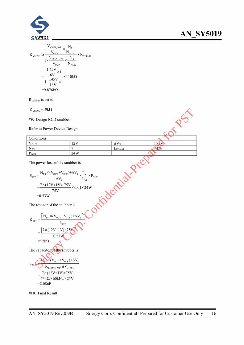
AN_SY5019 Rev.0.9B Silergy Corp. Confidential- Prepared for Customer Use Only 16
VSEN_OVP S
OVP AUX
VSEND VSENU
VSEN_OVP S
OVP AUX
V N
V NR R
V N1-
V N
1.45V1
16V= 110kΩ1.45V
1- 116V
=9.876kΩ
×≥ ×
×
××
×
RVSEND is set to
VSENDR =10kΩ
#9. Design RCD snubber
Refer to Power Device Design
Conditions
VOUT 12V ∆VS 75V
NPS 7 LK/LM 1%
POUT 24W
The power loss of the snubber is
PS OUT D_F S K
RCD OUT
S M
N (V +V )+∆V LP = P
∆V L
7 (12V+1V)+75V= 0.01 24W
75V
=0.53W
×× ×
× × ×
The resistor of the snubber is
[ ]
2
PS OUT D_F S
RCD
RCD
2
N (V +V )+∆VR =
P
7 (12V+1V)+75V=
0.53W
=52kΩ
×
×
The capacitor of the snubber is
PS OUT D_F S
RCD
RCD S_MIN C_RCD
N (V +V )+∆VC =
R f ∆V
7 (12V+1V)+75V=
53kΩ 60kHz 25V
=2.08nF
×
×× ×
#10. Final Result
Silerg
y Cor
p. Con
fiden
tial-P
repare
d for
PST

AN_SY5019
AN_SY5019 Rev.0.9B Silergy Corp. Confidential- Prepared for Customer Use Only 17
Fig.9 Final Result
Silerg
y Cor
p. Con
fiden
tial-P
repare
d for
PST

AN_SY5019
AN_SY5019 Rev.0.9B Silergy Corp. Confidential- Prepared for Customer Use Only 18
SO8 Package Outline & PCB Layout Design
5.4
0
0.60
1.27 TYP 1.5
5
5.4
0
0.60
1.27 TYP 1.5
5
0.30 – 0.50
5.8
0 -
6.1
0
3.8
0 -
4.0
0
0.30 – 0.50
5.8
0 -
6.2
0
3.8
0 -
4.0
0
Recommended Pad Layout
45°
0.2
5 b
ase
0 -8°°°°
0.1
8 -
0.2
5
0.25 - 0.50
0.60 - 0.85
45°
0.2
5 b
ase
0 -8°°°°
0.1
8 -
0.2
5
0.25 - 0.50
0.60 - 0.85 1.27 (TYP)
1.4
0 -
1.6
0
0.0
8 -
0.2
54.80 - 5.00
1.27 (TYP)
1.4
0 -
1.6
0
0.0
8 -
0.2
54.80 - 5.00
Notes: All dimensions are in millimeters.
All dimensions don’t include mold flash & metal burr.
Silerg
y Cor
p. Con
fiden
tial-P
repare
d for
PST


![[MS-PST]: Outlook Personal Folders (.pst) File Format · 2019-03-21 · [MS-PST]: Outlook Personal Folders (.pst) File Format Intellectual Property Rights Notice for Open Specifications](https://img.pdfslide.us/doc/110x75/5eccceeec221095fc21e2a35/ms-pst-outlook-personal-folders-pst-file-format-2019-03-21-ms-pst-outlook.jpg)


![[MS-PST]: Outlook Personal Folders (.pst) File Format · 2016-09-14 · [MS-PST]: Outlook Personal Folders (.pst) File Format Intellectual Property Rights Notice for Open Specifications](https://img.pdfslide.us/doc/110x75/5f6c9e9b4e11ae13a90bf845/ms-pst-outlook-personal-folders-pst-file-format-2016-09-14-ms-pst-outlook.jpg)
![[MS-PST]: Outlook Personal Folders (.pst) File Format · [MS-PST]: Outlook Personal Folders (.pst) File Format Intellectual Property Rights Notice for Open Specifications Documentation](https://img.pdfslide.us/doc/110x75/5e8f5f3d7d0a0a79de358e44/ms-pst-outlook-personal-folders-pst-file-format-ms-pst-outlook-personal.jpg)