Embed Size (px)
Citation preview

8/7/2019 Signal integrity and circuit reliability issues in deep
http://slidepdf.com/reader/full/signal-integrity-and-circuit-reliability-issues-in-deep 1/19
B . Karuna Kumari
EC094106
INTERCONNECT ISSUES(SIGNAL
INTEGRITY AND CIRCUIT
RELIABILITY )

8/7/2019 Signal integrity and circuit reliability issues in deep
http://slidepdf.com/reader/full/signal-integrity-and-circuit-reliability-issues-in-deep 2/19
Introduction
Interconnect parasitic
Capacitance
Resistance
Inductance
Design Techniques
Signal integrity issues
References
Contents

8/7/2019 Signal integrity and circuit reliability issues in deep
http://slidepdf.com/reader/full/signal-integrity-and-circuit-reliability-issues-in-deep 3/19
INTRODUCTION
A dvances in interconnect technologies, Such as
the increase in the number of metal layers,
stacked vias , and the reduced routing pitch,
have played a key role to continuously improveIC density and operating speed.
This inter connect in DSM suddenly controlled
timing power, noise design and reliability of the
circuit.

8/7/2019 Signal integrity and circuit reliability issues in deep
http://slidepdf.com/reader/full/signal-integrity-and-circuit-reliability-issues-in-deep 4/19
The problems that are associated with interconnect
are characterized as mainly two main issues
1. Circuit Reliability 2. Signal integrity
Circuit reliability refers to expected lifespan of
operation of a functioning system under nominal
conditions Here signal integrity includes timing, power ,
noise , design functionality.
Characterization of interconnect effect

8/7/2019 Signal integrity and circuit reliability issues in deep
http://slidepdf.com/reader/full/signal-integrity-and-circuit-reliability-issues-in-deep 5/19
Interconnect introduces three types of parasitic
effects
Capacitive
Resistive
Inductive
The above three parasitic influence the signal
integrity and degrade the performance of the circuit .
Here capacitance introduces the cross talk
Resistance introduces ohmic voltage drop
Inductance introduces L di/dt voltage drop
Interconnect parasitic :

8/7/2019 Signal integrity and circuit reliability issues in deep
http://slidepdf.com/reader/full/signal-integrity-and-circuit-reliability-issues-in-deep 6/19
Capacitance and crosstalk
A n unwanted coupling from a neighboring signal wire
to a n/w node introduces an interference called
crosstalk . This disturbance acts as noise source . In IC·s the
inter signal coupling can be both capacitive and
inductive.
The potential impact of capacitive crosstalk isinfluenced by the impedance of the line under
examination.
Analyzation of low interconnect affects
the circuit operation:

8/7/2019 Signal integrity and circuit reliability issues in deep
http://slidepdf.com/reader/full/signal-integrity-and-circuit-reliability-issues-in-deep 7/19
X
Y V X
C XY
C Y
If the line is floating the disturbance
caused by coupling persists .
Floating lines

8/7/2019 Signal integrity and circuit reliability issues in deep
http://slidepdf.com/reader/full/signal-integrity-and-circuit-reliability-issues-in-deep 8/19
Capacitive crosstalk may result in a data
dependence variation of propagation delay.
Cc
DELAY DEPENDENT
UPON A CTIVITY IN
NEIGHBORING WIRES
Cross Talk and Performance

8/7/2019 Signal integrity and circuit reliability issues in deep
http://slidepdf.com/reader/full/signal-integrity-and-circuit-reliability-issues-in-deep 9/19
Avoid floating nodes . Nodes sensitive to crosstalk
problems such as precharged busses, should be
equipped with keeper devices to reduce the
impedance.
Do not allow capacitance b/n two signal wires to
grow too large parallel wires on the same layer
should be spaced sufficiently.
Design Technique
Dealing with capacitive crosstalk
8/7/2019 Signal integrity and circuit reliability issues in deep
http://slidepdf.com/reader/full/signal-integrity-and-circuit-reliability-issues-in-deep 10/19
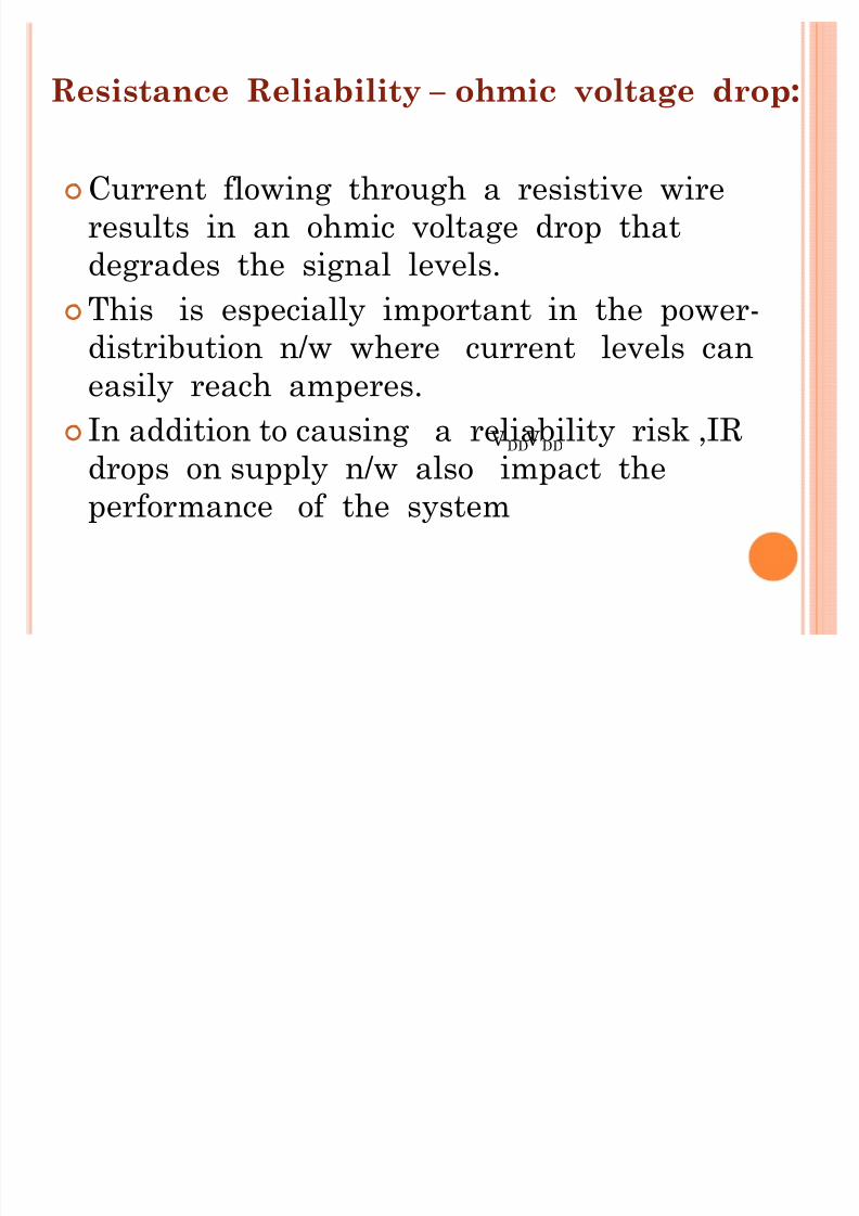
Current flowing through a resistive wire
results in an ohmic voltage drop that
degrades the signal levels.
This is especially important in the power-distribution n/w where current levels can
easily reach amperes.
In addition to causing a reliability risk ,IR
drops on supply n/w also impact the
performance of the system
VDDV
DD
Resistance Reliability ² ohmic voltage drop:

8/7/2019 Signal integrity and circuit reliability issues in deep
http://slidepdf.com/reader/full/signal-integrity-and-circuit-reliability-issues-in-deep 11/19
The delay of a wire grows drastically with its
length, doubling the length of a wire increases
its delay by a factor of 4!
The signal delay of long wires therefore tends
to be dominated by the RC effect.
This leads to the rather strange situation thatit may take multiple clock cycles to get a signal
from one side of a chip to its opposite end
Resistance and performance ² RC Delay
8/7/2019 Signal integrity and circuit reliability issues in deep
http://slidepdf.com/reader/full/signal-integrity-and-circuit-reliability-issues-in-deep 12/19
A first option for reducing RC delays is to use
better interconnect materials when they are
available and appropriate.
The introduction of silicides and Copper have
helped to reduce the resistance of poly silicon and
metal wires, respectively, while the adoption of
dielectric materials with a lower permittivity lowers
the capacitance.
Both Copper and low-permittivity dielectrics have
become common in advanced CMOS technologies
Better Interconnect Materials

8/7/2019 Signal integrity and circuit reliability issues in deep
http://slidepdf.com/reader/full/signal-integrity-and-circuit-reliability-issues-in-deep 13/19
Inductance and Reliability- L di/dt voltage drop:
Both VDD and VSS connections are routed to the external
supplies through bonding wires and package pins and possess
a non ignorable series inductance. Hence, a change in the
transient current creates a voltage difference b/w the
external and internal (V
DD·,G
ND·) supply voltages.
CL
V¶DD
V DD
L i(t)
VoutV in
GND 
L
Impact of inductance on
supply voltages:
�
Change in current inducesa change in voltage
� Longer supply lines have
larger L
8/7/2019 Signal integrity and circuit reliability issues in deep
http://slidepdf.com/reader/full/signal-integrity-and-circuit-reliability-issues-in-deep 14/19
Dealing with L di/dt
Separate power pins for I/O pads and chip core.
Multiple power and ground pins.
Careful selection of the positions of the power and
ground pins on the package.
Increase the rise and fall times of the off-chip signals to
the maximum extent allowable.
Schedule current-consuming transitions.
Use advanced packaging technologies.

8/7/2019 Signal integrity and circuit reliability issues in deep
http://slidepdf.com/reader/full/signal-integrity-and-circuit-reliability-issues-in-deep 15/19
Chip level design challenges dominated by
interconnect Issues are
a) power and
b) clock distribution
Power The conditions contributing to the
complexity of power distribution systems are
primarily due to interconnect and its impact on
chip performance.
8/7/2019 Signal integrity and circuit reliability issues in deep
http://slidepdf.com/reader/full/signal-integrity-and-circuit-reliability-issues-in-deep 16/19
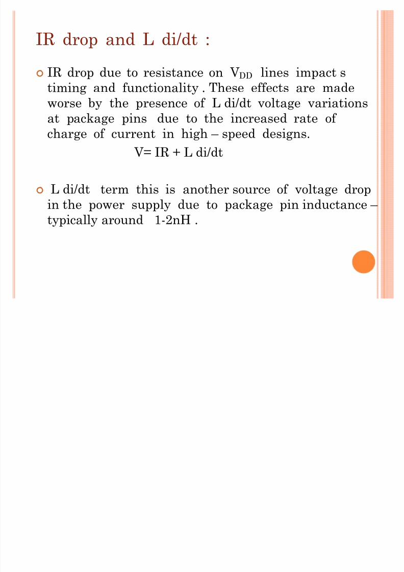
IR drop due to resistance on V lines impact stiming and functionality . These effects are made
worse by the presence of L di/dt voltage variations
at package pins due to the increased rate of
charge of current in high ² speed designs.
V= IR + L di/dt
L di/dt term this is another source of voltage drop
in the power supply due to package pin inductance ²
typically around 1-2nH .
IR drop and L di/dt :
DD

8/7/2019 Signal integrity and circuit reliability issues in deep
http://slidepdf.com/reader/full/signal-integrity-and-circuit-reliability-issues-in-deep 17/19
V OLTAGE DROPS
Voltage drop on the power grid primarily effect
timing
Noise margin of logic gates, due to only the
voltage drops in power grid, but also increase involtage in ground grid.
Once the noise margins drop below the budgeted
amount, typically 10% the design not guaranteed
to operated properly.
8/7/2019 Signal integrity and circuit reliability issues in deep
http://slidepdf.com/reader/full/signal-integrity-and-circuit-reliability-issues-in-deep 18/19
Clock distribution A ll sequential circuitshave one property in common ²a well-definedordered of the switching events must beimposed if the circuit is to operate correctly.
The synchronous system approach ,in which allmemory elements in the system aresimultaneously updated using a globallydistributed periodic synchronization signal(that is, a global clock signal), represents an
effective and popular way to enforce thisordering.
8/7/2019 Signal integrity and circuit reliability issues in deep
http://slidepdf.com/reader/full/signal-integrity-and-circuit-reliability-issues-in-deep 19/19
Challenges & Solutions of Signal Integrity in VDSM
Physical Design Dr. Danny Rittman
([email protected]) May 2004 Digital Integrated Circuits A Design Perspective
by Jan M.Rabaey .
A nalysis and design of Digital Integrated circuits In
deep Submicron Technology by David A Hodges|Horace G Jackson | Resve A saleh
References