Embed Size (px)
Citation preview
www.yc-dz.com
1 04/07/00
DATA SHEET SigmaTel, Inc. Integrating Mixed-Signal Solutions STAC9721/23
Stereo AC'97 Codec With Multi-Codec Option
GENERAL DESCRIPTION:
SigmaTel’s STAC9721/23 is a general-purpose 18-bit stereo, full duplex, audio codec that conforms to the analog component specification of AC'97 (Audio Codec 97 Component Specification Rev. 2.1). The STAC9721/23 incorporates SigmaTel’s proprietary Sigma-Delta technology to achieve a DAC SNR in excess of 95dB. The DACs, ADCs, and mixer are integrated with analog I/Os, which include four analog line-level stereo inputs, two analog line-level mono inputs, two stereo outputs, and one mono output channel. Also included are SigmaTel’s 3D stereo enhancement (SS3D), and an extra true line-level out for headphones or speaker amplifiers. The STAC9721/23 may be used as a secondary codec, with the STAC9700/04/07/44/45 or a 4-channel STAC9708 as the primary, in multiple codec configurations conforming to the AC'97 Rev. 2.1 specification. This configuration can provide up to six-channel output, providing AC-3 playback for DVD applications. The STAC9721/23 communicates via the five-wire AC-Link interface with any AC-Link capable controller or advanced core logic chip-set. Packaged in an AC'97 compliant 48-pin TQFP, the STAC9721/23 can be placed on motherboards, daughter boards, add-on cards or AMR/MDC cards.
FEATURES:
• High performance ΣΣΣΣ∆∆∆∆ technology
• Energy saving power down modes
• 18-bit full duplex stereo ADC, DACs
• AC-Link protocol compliance
• 3.3V Multiple power supply options
• Pin compatible with the STAC9700/44/45
• SigmaTel Surround (SS3D) Stereo Enhancement
• EAPD – External Amplifier Power Down Control
• Multi-Codec option (Intel AC'97 rev 2.1)
• Six analog line-level inputs
• 48-pin TQFP
• LINE-to-LINE SNR 102dB
• The STAC9723 is tested at +3.3V
ORDERING INFORMATION:
PART NUMBER
PACKAGE TEMPERATURE RANGE
SUPPLY RANGE
STAC9721T 48-pin TQFP 7mm x7mm x 1.4mm 0o C to +70o C DVdd = 3.3V or 5V, AVdd = 5V
STAC9723T 48-pin TQFP 7mmx7mm x 1.4mm 0o C to +70o C DVdd = 3.3V, AVdd = 3.3V
SigmaTel reserves the right to change specifications without notice
www.yc-dz.com
SigmaTel, Inc. Datasheet STAC9721/23
2 04/07/00 04/07/00
Table of Contents GENERAL DESCRIPTION:.........................1
TABLE OF CONTENTS................................2
TABLE OF CONTENTS – FIGURES..........3
1. PIN/SIGNAL DESCRIPTIONS .............7
1.1 DIGITAL I/O 7
1.2 ANALOG I/O 8
1.3 FILTER/REFERENCES/GPIO 9
1.4 POWER AND GROUND SIGNALS 9
2. AC-LINK ................................................10
2.1 CLOCKING 10
2.2 RESET 10
3. DIGITAL INTERFACE........................11
3.1 AC-LINK SERIAL INTERFACE 11
3.2 AC-LINK LOW POWER MODE 18
4. STAC9721/23 MIXER...........................19
4.1 MIXER INPUT 20
4.2 MIXER OUTPUT 20
4.3 PC BEEP IMPLEMENTATION 20
4.4 PROGRAMMING REGISTERS: 21
5. LOW POWER MODES........................29
6. MULTIPLE CODEC SUPPORT .........31
6.1 PRIMARY/SECONDARY CODEC 31
6.2 SECONDARY CODEC ACCESS 32
7. TESTABILITY ......................................32
8. EXTENDED FUNCTIONALITY ........33
8.1 ANTI-POP CIRCUITRY 33
9. AC TIMING CHARACTERISTICS .33
9.1 COLD RESET 33
9.2 WARM RESET 34
9.3 CLOCKS 34
9.4 DATA SETUP AND HOLD 35
9.5 SIGNAL RISE AND FALL 35
9.6 AC-LINK LOW POWER MODE 36
9.7 ATE TEST MODE 37
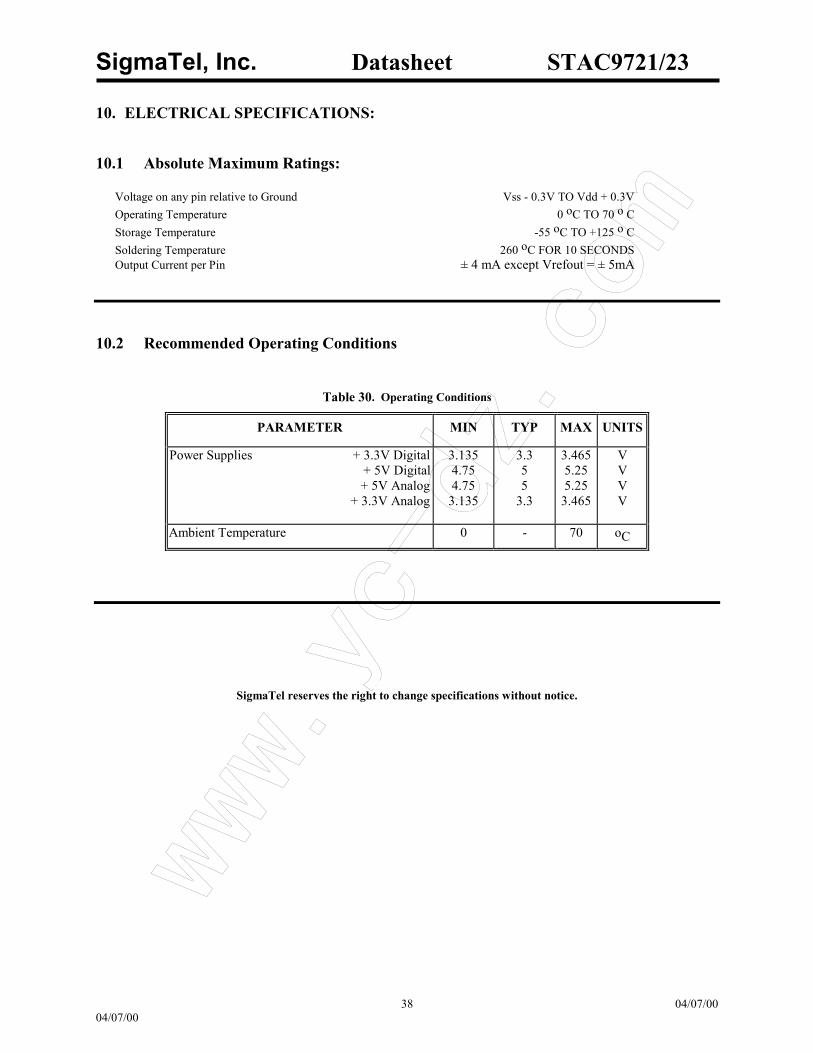
10. ELECTRICAL SPECIFICATIONS: ...38
10.1 MAXIMUM RATINGS: 38
10.2 RECOMMENDED CONDITIONS 38
10.3 POWER CONSUMPTION 39
10.4 AC-LINK STATIC DIGITAL 41
10.5 STAC9721 ANALOG 41
10.6 STAC9723 ANALOG 43
APPENDIX A................................................45
APPENDIX B ................................................46 TABLE of Tables
Table 1. Package Dimensions 4
Table 2. Pin Designation 4
Table 3. Digital Signal List 7
Table 4. Analog Signal List 8
Table 5. Filtering and Voltage References 9
Table 6. Mixer Functional Connections 20
Table 7. Programming Registers 21
Table 8. Play Master Volume Register 22
Table 9. PC_BEEP Register 22
Table 10. Analog Mixer Input Gain Register 23
Table 11. Record Select Control Registers 23
Table 12. Left Record Select Control Registers 23
Table 13. Record Gain Registers 24
Table 14. General Purpose Register 24
Table 15. 3D Control Registers Error! Bookmark
not defined.
Table 16. Powerdown Status Registers 25
Table 17. Extended Audio ID Functions 26
Table 19: Analog Current Adjust 27
Table 16. Multi-Channel Programming 28
Table 18. Low Power Modes 29
Table 19. Codec ID Selection 31
Table 20. Secondary Codec Register Access 32
www.yc-dz.com
SigmaTel, Inc. Datasheet STAC9721/23
3 04/07/00 04/07/00
Table 21. Cold Reset 33
Table 22. Warm Reset 34
Table 23. Clocks 34
Table 24. Data Setup and Hold 35
Table 25. Signal Rise and Fall Times 35
Table 26. AC-Link Low Power Mode Timing 36
Table 27. ATE Test Mode 37
Table 28. Operating Conditions 38
Table 33: Power Consumption 39
Table 34: Power Consumption at 3.3V Analog 39
Table 35: Reduced Analog Power Settings 40
Table 30. AC-Link Static Specifications 41
Table 31. Analog Performance Characteristics 41
Table 32. Analog Performance Characteristics 43 Table of Contents – Figures
Figure 1. Package Outline ..................................... 4
Figure 2. STAC9721/23 Block Diagram............... 5
Figure 3. AC-Link to its companion controller .. 10
Figure 4. Bi-directional Audio Frame ................. 12
Figure 5. AC-Link Audio Output Frame .......... 12
Figure 6. Start of an Audio Output Frame ....... 13
Figure 7. STAC9721/23 Audio Input Frame ..... 16
Figure 8. Start of an Audio Input Frame ........... 16
Figure 9. STAC9721/23 Powerdown Timing ..... 18
Figure 10. STAC9721/23 Mixer ......................... 19
Figure 11. Powerdown/Powerup flow.................. 29
Figure 12. Powerdown/Powerup flow ................. 30
Figure 13. Cold Reset........................................... 33
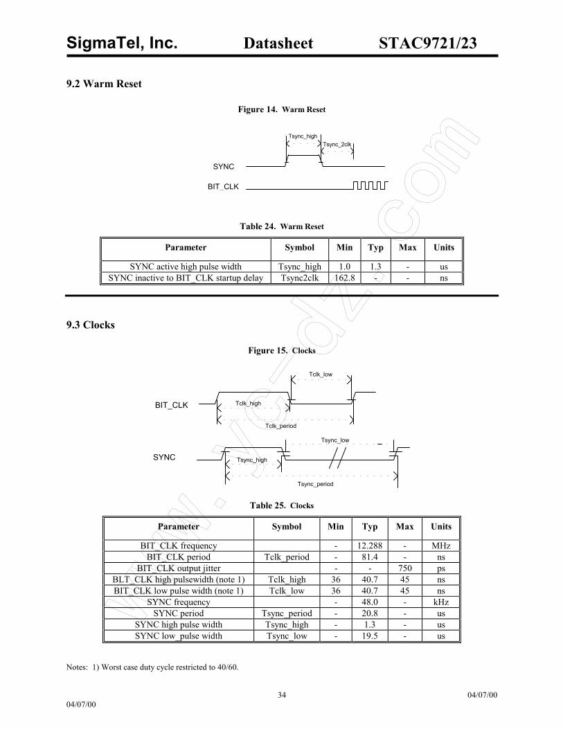
Figure 14. Warm Reset ........................................ 34
Figure 15. Clocks.................................................. 34
Figure 16. Data Setup and Hold.......................... 35
Figure 17. Signal Rise and Fall Times ................ 35
Figure 18. AC-Link Low Power Mode Timing.. 36
Figure 19. ATE Test Mode .................................. 37
www.yc-dz.com
SigmaTel, Inc. Datasheet STAC9721/23
4 04/07/00 04/07/00
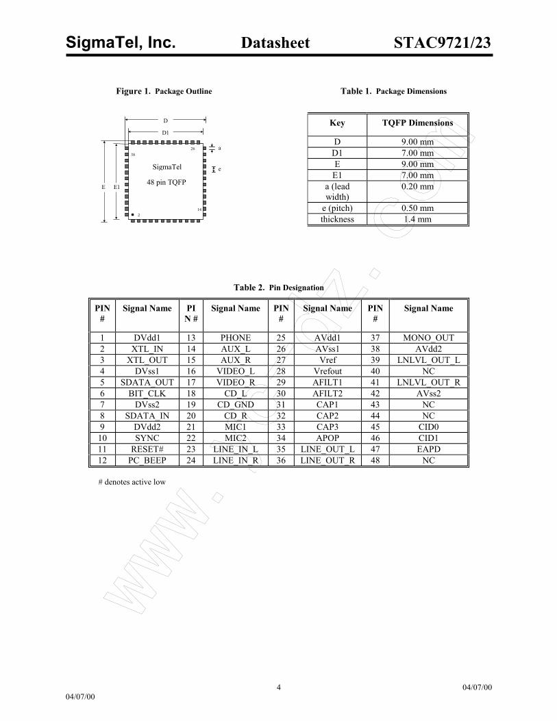
Figure 1. Package Outline
SigmaTel
48 pin TQFP
a
D1
D
e
E1E
3826
142
Table 1. Package Dimensions
Key TQFP Dimensions
D 9.00 mm D1 7.00 mm E 9.00 mm
E1 7.00 mm a (lead width)
0.20 mm
e (pitch) 0.50 mm thickness 1.4 mm
Table 2. Pin Designation
PIN #
Signal Name PIN #
Signal Name PIN #
Signal Name PIN #
Signal Name
1 DVdd1 13 PHONE 25 AVdd1 37 MONO_OUT 2 XTL_IN 14 AUX_L 26 AVss1 38 AVdd2 3 XTL_OUT 15 AUX_R 27 Vref 39 LNLVL_OUT_L 4 DVss1 16 VIDEO_L 28 Vrefout 40 NC 5 SDATA_OUT 17 VIDEO_R 29 AFILT1 41 LNLVL_OUT_R 6 BIT_CLK 18 CD_L 30 AFILT2 42 AVss2 7 DVss2 19 CD_GND 31 CAP1 43 NC 8 SDATA_IN 20 CD_R 32 CAP2 44 NC 9 DVdd2 21 MIC1 33 CAP3 45 CID0
10 SYNC 22 MIC2 34 APOP 46 CID1 11 RESET# 23 LINE_IN_L 35 LINE_OUT_L 47 EAPD 12 PC_BEEP 24 LINE_IN_R 36 LINE_OUT_R 48 NC
# denotes active low
www.yc-dz.com
SigmaTel, Inc. Datasheet STAC9721/23
5 04/07/00 04/07/00
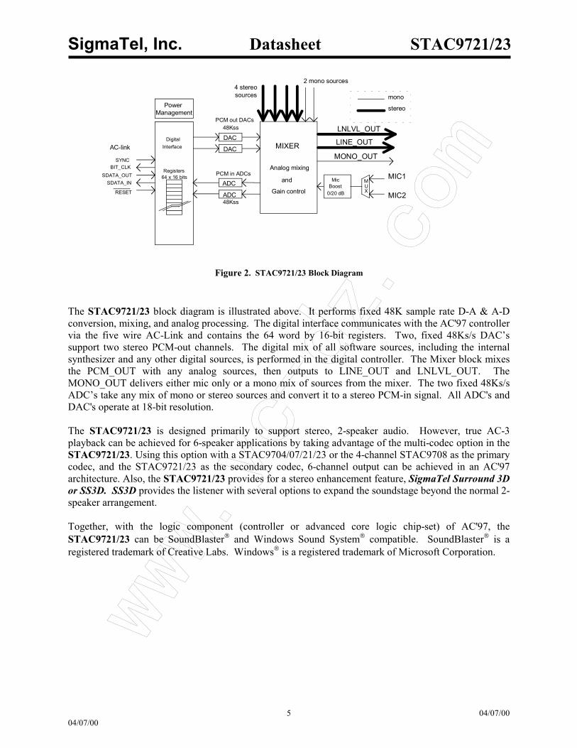
Figure 2. STAC9721/23 Block Diagram
The STAC9721/23 block diagram is illustrated above. It performs fixed 48K sample rate D-A & A-D conversion, mixing, and analog processing. The digital interface communicates with the AC'97 controller via the five wire AC-Link and contains the 64 word by 16-bit registers. Two, fixed 48Ks/s DAC’s support two stereo PCM-out channels. The digital mix of all software sources, including the internal synthesizer and any other digital sources, is performed in the digital controller. The Mixer block mixes the PCM_OUT with any analog sources, then outputs to LINE_OUT and LNLVL_OUT. The MONO_OUT delivers either mic only or a mono mix of sources from the mixer. The two fixed 48Ks/s ADC’s take any mix of mono or stereo sources and convert it to a stereo PCM-in signal. All ADC's and DAC's operate at 18-bit resolution. The STAC9721/23 is designed primarily to support stereo, 2-speaker audio. However, true AC-3 playback can be achieved for 6-speaker applications by taking advantage of the multi-codec option in the STAC9721/23. Using this option with a STAC9704/07/21/23 or the 4-channel STAC9708 as the primary codec, and the STAC9721/23 as the secondary codec, 6-channel output can be achieved in an AC'97 architecture. Also, the STAC9721/23 provides for a stereo enhancement feature, SigmaTel Surround 3D or SS3D. SS3D provides the listener with several options to expand the soundstage beyond the normal 2-speaker arrangement. Together, with the logic component (controller or advanced core logic chip-set) of AC'97, the STAC9721/23 can be SoundBlaster and Windows Sound System compatible. SoundBlaster is a registered trademark of Creative Labs. Windows is a registered trademark of Microsoft Corporation.
LINE_OUT
MONO_OUT
MIC1
MIC2
MUX
MIXER
Analog mixing
and
Gain control
DAC
DAC
ADC
ADC
PowerManagement
DigitalInterface
Registers64 x 16 bits Mic
Boost0/20 dB
PCM out DACs
PCM in ADCs
AC-link
4 stereosources
2 mono sources
mono
stereo
48Kss
48Kss
SYNCBIT_CLK
SDATA_OUTSDATA_IN
RESET
LNLVL_OUT
www.yc-dz.com
SigmaTel, Inc. Datasheet STAC9721/23
6 04/07/00 04/07/00
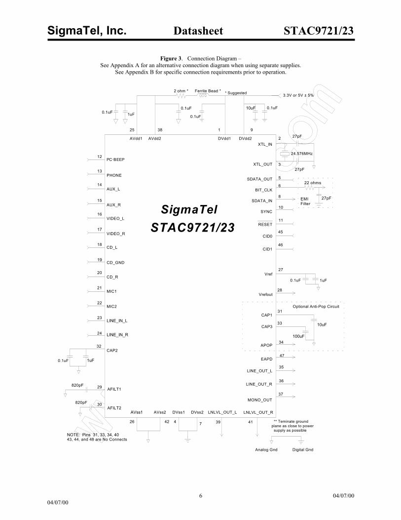
Figure 3. Connection Diagram – See Appendix A for an alternative connection diagram when using separate supplies.
See Appendix B for specific connection requirements prior to operation.
VIDEO_L
VIDEO_R
AUX_L
AFILT1
AFILT2AVss1 AVss2 DVss1 DVss2
AVdd1 AVdd2 DVdd1 DVdd2
Ferrite Bead *2 ohm *
0.1uF 10uF1uF 0.1uF
0.1uF0.1uF
820pF
29
30
14
17
16
25 38 1 9
744226
3
2
CAP2
XTL_OUT
XTL_IN
3.3V or 5V ± 5%
24.576MHz
32
1uF
SigmaTelSTAC9721/23
28Vrefout
Vref27
1uF0.1uF
27pF
27pF
LINE_OUT_L
LINE_OUT_R
MONO_OUT
35
36
37
LINE_IN_R24
LINE_IN_L23
PHONE13
PC_BEEP12
MIC222
AUX_R15
MIC121
6
5
8
11
10
SDATA_OUT
SDATA_IN
RESET
SYNC
BIT_CLK
CD_GND
CD_R20
19
18CD_L
Analog Gnd Digital Gnd
NOTE: Pins 31, 33, 34, 4043, 44, and 48 are No Connects
* Suggested
** Teminate groundplane as close to power
supply as possible
LNLVL_OUT_L LNLVL_OUT_R
39 41
46
45
CID1
CID0
820pF
APOP
EAPD
34
47
CAP131
CAP333
0.1uF
Optional Anti-Pop Circuit
100uF
10uF
27pF
22 ohms
EMIFilter
www.yc-dz.com
SigmaTel, Inc. Datasheet STAC9721/23
7 04/07/00 04/07/00
1. PIN/SIGNAL DESCRIPTIONS
1.1 Digital I/O These signals connect the STAC9721/23 to its AC'97 controller counterpart, an external crystal, multi-codec selection and external audio amplifier.
Table 3. Digital Signal List
Signal Name Type Description
RESET # I AC'97 Master H/W Reset
XTL_IN I 24.576 MHz Crystal
XTL_OUT O 24.576 MHz Crystal
SYNC I 48 kHz fixed rate sample sync
BIT_CLK O 12.288 MHz serial data clock
SDATA_OUT I Serial, time division multiplexed, AC'97 input stream
SDATA__IN O Serial, time division multiplexed, AC'97 output stream
CID0 I Multi-Codec ID select – bit 0
CID1 I Multi-Codec ID select – bit 1
EAPD O External Amplifier Power Down
# denotes active low
www.yc-dz.com
SigmaTel, Inc. Datasheet STAC9721/23
8 04/07/00 04/07/00
1.2 Analog I/O These signals connect the STAC9721/23 to analog sources and sinks, including microphones and speakers.
Table 4. Analog Signal List
Signal Name Type Description
PC-BEEP I PC Speaker beep pass-through
PHONE I From telephony subsystem speakerphone (or DLP - Down Line Phone)
MIC1 I Desktop Microphone Input
MIC2 I Second Microphone Input
LINE-IN-L I Line In Left Channel
LINE-IN-R I Line In Right Channel
CD-L I CD Audio Left Channel
CD-GND I CD Audio analog ground
CD-R I CD Audio Right Channel
VIDEO-L I Video Audio Left Channel
VIDEO-R I Video Audio Right Channel
AUX-L I Aux Left Channel
AUX-R I Aux Right Channel
LINE-OUT-L O Line Out Left Channel
LINE-OUT-R O Line Out Right Channel
MONO-OUT O To telephony subsystem speakerphone (or DLP – Down Line Phone)
LNLVL_OUT_L
O True Line Level Out Left Channel
LNLVL_OUT_R
O True Line Level Out Right Channel
* Note: any unused input pins should be tied together and connected to ground with a capacitor (0.1 uF suggested), except the MIC1 and MIC2 inputs which require their own 0.1 uF capacitors to ground if not used.
www.yc-dz.com
SigmaTel, Inc. Datasheet STAC9721/23
9 04/07/00 04/07/00
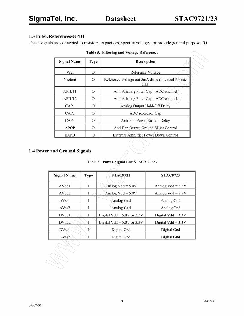
1.3 Filter/References/GPIO These signals are connected to resistors, capacitors, specific voltages, or provide general purpose I/O.
Table 5. Filtering and Voltage References
Signal Name Type Description
Vref O Reference Voltage
Vrefout O Reference Voltage out 5mA drive (intended for mic bias)
AFILT1 O Anti-Aliasing Filter Cap - ADC channel
AFILT2 O Anti-Aliasing Filter Cap - ADC channel
CAP1 O Analog Output Hold-Off Delay
CAP2 O ADC reference Cap
CAP3 O Anti-Pop Power Sustain Delay
APOP O Anti-Pop Output Ground Shunt Control
EAPD O External Amplifier Power Down Control
1.4 Power and Ground Signals
Table 6. Power Signal List STAC9721/23
Signal Name Type STAC9721 STAC9723
AVdd1 I Analog Vdd = 5.0V Analog Vdd = 3.3V
AVdd2 I Analog Vdd = 5.0V Analog Vdd = 3.3V
AVss1 I Analog Gnd Analog Gnd
AVss2 I Analog Gnd Analog Gnd
DVdd1 I Digital Vdd = 5.0V or 3.3V Digital Vdd = 3.3V
DVdd2 I Digital Vdd = 5.0V or 3.3V Digital Vdd = 3.3V
DVss1 I Digital Gnd Digital Gnd
DVss2 I Digital Gnd Digital Gnd
www.yc-dz.com
SigmaTel, Inc. Datasheet STAC9721/23
10 04/07/00 04/07/00
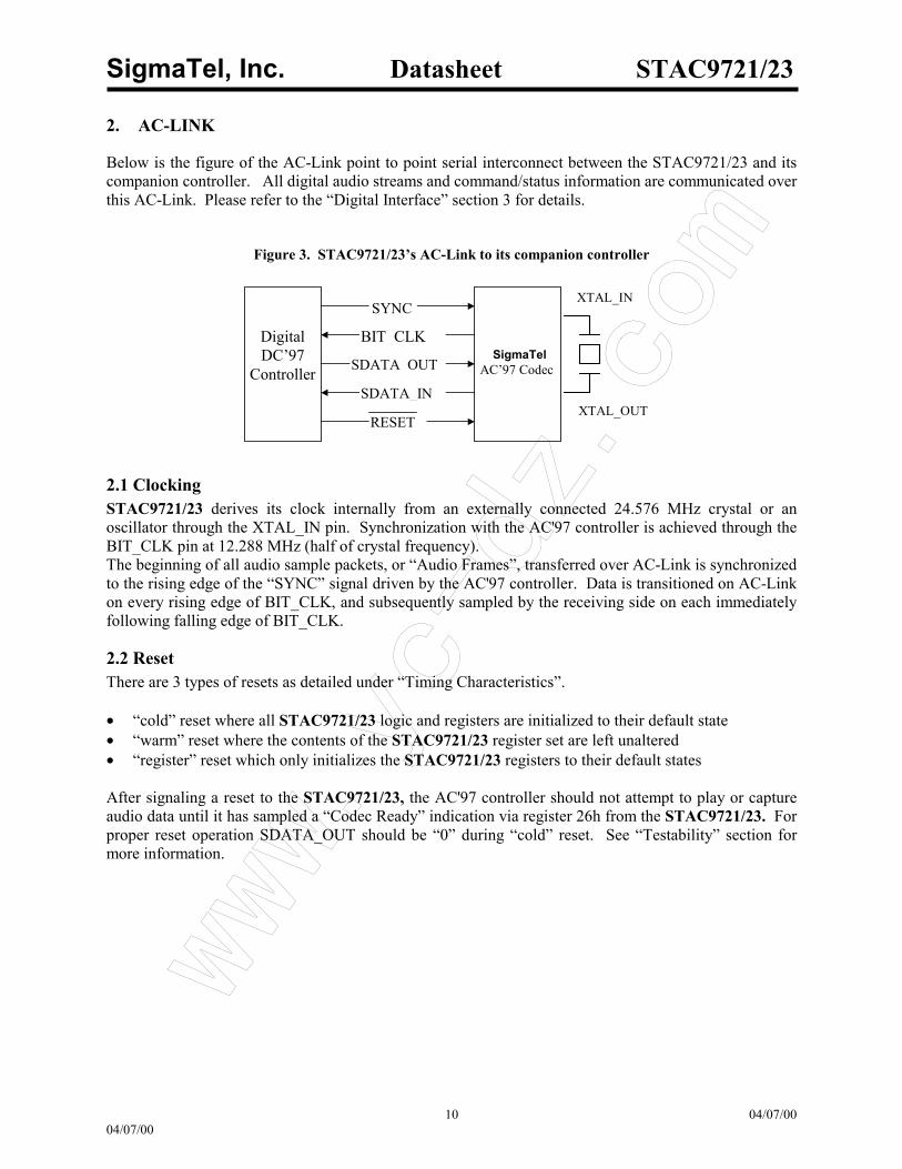
2. AC-LINK
Below is the figure of the AC-Link point to point serial interconnect between the STAC9721/23 and its companion controller. All digital audio streams and command/status information are communicated over this AC-Link. Please refer to the “Digital Interface” section 3 for details.
Figure 3. STAC9721/23’s AC-Link to its companion controller
SYNC
BIT CLK
SDATA_OUT
SDATA_IN
RESET
DigitalDC’97
ControllerSigmaTel
AC’97 Codec
XTAL_IN
XTAL_OUT
2.1 Clocking STAC9721/23 derives its clock internally from an externally connected 24.576 MHz crystal or an oscillator through the XTAL_IN pin. Synchronization with the AC'97 controller is achieved through the BIT_CLK pin at 12.288 MHz (half of crystal frequency). The beginning of all audio sample packets, or “Audio Frames”, transferred over AC-Link is synchronized to the rising edge of the “SYNC” signal driven by the AC'97 controller. Data is transitioned on AC-Link on every rising edge of BIT_CLK, and subsequently sampled by the receiving side on each immediately following falling edge of BIT_CLK.
2.2 Reset
There are 3 types of resets as detailed under “Timing Characteristics”. • “cold” reset where all STAC9721/23 logic and registers are initialized to their default state • “warm” reset where the contents of the STAC9721/23 register set are left unaltered • “register” reset which only initializes the STAC9721/23 registers to their default states After signaling a reset to the STAC9721/23, the AC'97 controller should not attempt to play or capture audio data until it has sampled a “Codec Ready” indication via register 26h from the STAC9721/23. For proper reset operation SDATA_OUT should be “0” during “cold” reset. See “Testability” section for more information.
www.yc-dz.com
SigmaTel, Inc. Datasheet STAC9721/23
11 04/07/00 04/07/00
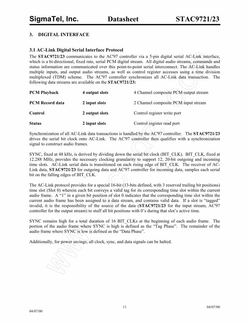
3. DIGITAL INTERFACE
3.1 AC-Link Digital Serial Interface Protocol The STAC9721/23 communicates to the AC'97 controller via a 5-pin digital serial AC-Link interface, which is a bi-directional, fixed rate, serial PCM digital stream. All digital audio streams, commands and status information are communicated over this point-to-point serial interconnect. The AC-Link handles multiple inputs, and output audio streams, as well as control register accesses using a time division multiplexed (TDM) scheme. The AC'97 controller synchronizes all AC-Link data transaction. The following data streams are available on the STAC9721/23: PCM Playback 4 output slots 4 Channel composite PCM output stream PCM Record data 2 input slots 2 Channel composite PCM input stream Control 2 output slots Control register write port Status 2 input slots Control register read port Synchronization of all AC-Link data transactions is handled by the AC'97 controller. The STAC9721/23 drives the serial bit clock onto AC-Link. The AC'97 controller then qualifies with a synchronization signal to construct audio frames. SYNC, fixed at 48 kHz, is derived by dividing down the serial bit clock (BIT_CLK). BIT_CLK, fixed at 12.288 MHz, provides the necessary clocking granularity to support 12, 20-bit outgoing and incoming time slots. AC-Link serial data is transitioned on each rising edge of BIT_CLK. The receiver of AC-Link data, STAC9721/23 for outgoing data and AC'97 controller for incoming data, samples each serial bit on the falling edges of BIT_CLK. The AC-Link protocol provides for a special 16-bit (13-bits defined, with 3 reserved trailing bit positions) time slot (Slot 0) wherein each bit conveys a valid tag for its corresponding time slot within the current audio frame. A “1” in a given bit position of slot 0 indicates that the corresponding time slot within the current audio frame has been assigned to a data stream, and contains valid data. If a slot is “tagged” invalid, it is the responsibility of the source of the data (STAC9721/23 for the input stream, AC'97 controller for the output stream) to stuff all bit positions with 0’s during that slot’s active time. SYNC remains high for a total duration of 16 BIT_CLKs at the beginning of each audio frame. The portion of the audio frame where SYNC is high is defined as the “Tag Phase”. The remainder of the audio frame where SYNC is low is defined as the “Data Phase”. Additionally, for power savings, all clock, sync, and data signals can be halted.
www.yc-dz.com
SigmaTel, Inc. Datasheet STAC9721/23
12 04/07/00 04/07/00
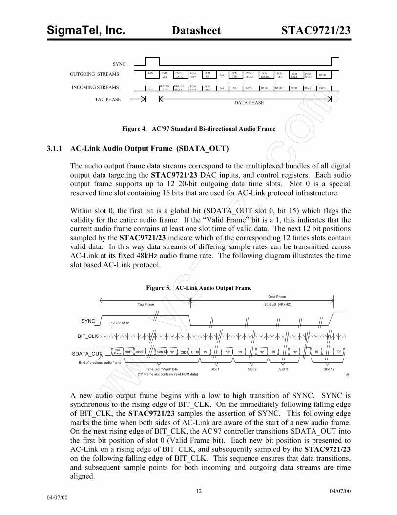
Figure 4. AC'97 Standard Bi-directional Audio Frame
3.1.1 AC-Link Audio Output Frame (SDATA_OUT)
The audio output frame data streams correspond to the multiplexed bundles of all digital output data targeting the STAC9721/23 DAC inputs, and control registers. Each audio output frame supports up to 12 20-bit outgoing data time slots. Slot 0 is a special reserved time slot containing 16 bits that are used for AC-Link protocol infrastructure. Within slot 0, the first bit is a global bit (SDATA_OUT slot 0, bit 15) which flags the validity for the entire audio frame. If the “Valid Frame” bit is a 1, this indicates that the current audio frame contains at least one slot time of valid data. The next 12 bit positions sampled by the STAC9721/23 indicate which of the corresponding 12 times slots contain valid data. In this way data streams of differing sample rates can be transmitted across AC-Link at its fixed 48kHz audio frame rate. The following diagram illustrates the time slot based AC-Link protocol.
Figure 5. AC-Link Audio Output Frame
SYNC
BIT_CLK
SDATA_OUTvalid
Frame slot1 slot2
End of previous audio frame
slot(12) "0" 19 "0" "0""0"19 19 19 "0"
Data Phase
20.8 uS (48 kHZ)Tag Phase
12.288 MHz
Time Slot "Valid" Bits Slot 1 Slot 2 Slot 3 Slot 12("1" = time slot contains valid PCM data)
CID1 CID0
e A new audio output frame begins with a low to high transition of SYNC. SYNC is synchronous to the rising edge of BIT_CLK. On the immediately following falling edge of BIT_CLK, the STAC9721/23 samples the assertion of SYNC. This following edge marks the time when both sides of AC-Link are aware of the start of a new audio frame. On the next rising edge of BIT_CLK, the AC'97 controller transitions SDATA_OUT into the first bit position of slot 0 (Valid Frame bit). Each new bit position is presented to AC-Link on a rising edge of BIT_CLK, and subsequently sampled by the STAC9721/23 on the following falling edge of BIT_CLK. This sequence ensures that data transitions, and subsequent sample points for both incoming and outgoing data streams are time aligned.
OUTGOING STREAMS
INCOMING STREAMS
SYNC
TAG PHASE
TAG CMDADR
CMDDATA
PCMLEFT
PCMRT NA RSVD
RSVDRSVDRSVDRSVDRSVDRSVDNA NAPCMLEFT
PCMRT
STATUSDATA
STATUSADRTAG
DATA PHASE
PCMCTR
PCMLSURR
PCMRSURR
PCMLFE
PCMLALT
PCMRALT
www.yc-dz.com
SigmaTel, Inc. Datasheet STAC9721/23
13 04/07/00 04/07/00
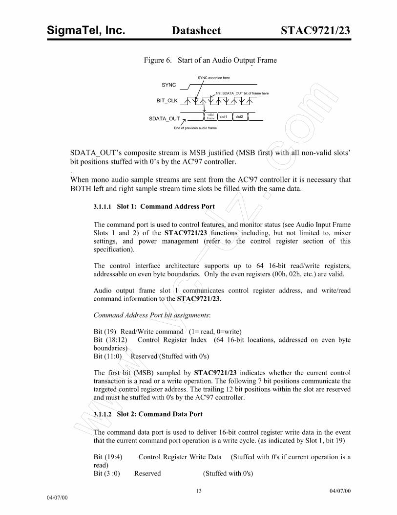
Figure 6. Start of an Audio Output Frame
SYNC
BIT_CLK
SDATA_OUT
first SDATA_OUT bit of frame here
SYNC assertion here
valid Frame slot1 slot2
End of previous audio frame SDATA_OUT’s composite stream is MSB justified (MSB first) with all non-valid slots’ bit positions stuffed with 0’s by the AC'97 controller. . When mono audio sample streams are sent from the AC'97 controller it is necessary that BOTH left and right sample stream time slots be filled with the same data.
3.1.1.1 Slot 1: Command Address Port
The command port is used to control features, and monitor status (see Audio Input Frame Slots 1 and 2) of the STAC9721/23 functions including, but not limited to, mixer settings, and power management (refer to the control register section of this specification). The control interface architecture supports up to 64 16-bit read/write registers, addressable on even byte boundaries. Only the even registers (00h, 02h, etc.) are valid. Audio output frame slot 1 communicates control register address, and write/read command information to the STAC9721/23. Command Address Port bit assignments: Bit (19) Read/Write command (1= read, 0=write) Bit (18:12) Control Register Index (64 16-bit locations, addressed on even byte boundaries) Bit (11:0) Reserved (Stuffed with 0's) The first bit (MSB) sampled by STAC9721/23 indicates whether the current control transaction is a read or a write operation. The following 7 bit positions communicate the targeted control register address. The trailing 12 bit positions within the slot are reserved and must he stuffed with 0's by the AC'97 controller. 3.1.1.2 Slot 2: Command Data Port The command data port is used to deliver 16-bit control register write data in the event that the current command port operation is a write cycle. (as indicated by Slot 1, bit 19) Bit (19:4) Control Register Write Data (Stuffed with 0's if current operation is a read) Bit (3 :0) Reserved (Stuffed with 0's)
www.yc-dz.com
SigmaTel, Inc. Datasheet STAC9721/23
14 04/07/00 04/07/00
If the current command port operation is a read then the entire slot time must be stuffed with 0's by the AC'97 controller. 3.1.1.3 Slot 3: PCM Playback Left Channel Audio output frame slot 3 is the composite digital audio left playback stream. In a typical “Games Compatible" PC this slot is composed of standard PCM (.wav) output samples digitally mixed (by the AC'97 controller or host processor) with music synthesis output samples. If a sample stream of resolution less than 20-bits is transferred, the AC'97 controller must stuff all trailing non-valid bit positions within this time slot with 0's. Please refer to the register programming section for details on the multi-channel programming options. 3.1.1.4 Slot 4: PCM Playback Right Channel Audio output frame slot 4 is the composite digital audio right playback stream. In a typical “Games Compatible" PC this slot is composed of standard PCM (.wav) output samples digitally mixed (by the AC'97 controller or host processor) with music synthesis output samples. If a sample stream of resolution less than 20-bits is transferred, the AC'97 controller must stuff all trailing non-valid bit positions within this time slot with 0's. Please refer to the register programming section for details on the multi-channel programming options. 3.1.1.5 Slot 5: Reserved Audio output frame slot 5 is reserved for modem operation and is not used by the STAC9721/23. 3.1.1.6 Slot 6: PCM Center Channel Audio output frame slot 6 is the composite digital audio center stream used in a multi-channel application where the STAC9721/23 has been programmed to accept the DAC PCM data from slots 6 and 9. Please refer to the register programming section for details on the multi-channel programming options. 3.1.1.7 Slot 7: PCM Left Surround Channel Audio output frame slot 7 is the composite digital audio left surround stream used in a multi-channel application where the STAC9721/23 has been programmed to accept the DAC PCM data from slots 7 and 8. Please refer to the register programming section for details on the multi-channel programming options. 3.1.1.8 Slot 8: PCM Right Surround Channel Audio output frame slot 8 is the composite digital audio right surround stream used in a multi-channel application where the STAC9721/23 has been programmed to accept the DAC PCM data from slots 7 and 8. Please refer to the register programming section for details on the multi-channel programming options.
www.yc-dz.com
SigmaTel, Inc. Datasheet STAC9721/23
15 04/07/00 04/07/00
3.1.1.9 Slot 9: PCM Low Frequency Channel Audio output frame slot 9 is the composite digital audio low frequency stream used in a multi-channel application where the STAC9721/23 has been programmed to accept the DAC DAC PCM data from slots 6 and 9. Please refer to the register programming section for details on the multi-channel programming options. 3.1.1.10 Slot 10: PCM Alternate Left Audio output frame slot 10 is the composite digital audio alternate left stream used in a multi-channel application where the STAC9721/23 has been programmed to accept the DAC PCM data from slots 10 and 11. Please refer to the register programming section for details on the multi channel programming options. 3.1.1.11 Slot 11: PCM Alternate Right Audio output frame slot 11 is the composite digital audio alternate right stream used in a multi-channel application where the STAC9721/23 has been programmed to accept the DAC PCM data from slots 10 and 11. Please refer to the register programming section for details on the multi channel programming options. 3.1.1.12 Slot 12: Reserved Audio output frame slot 12 is reserved for modem operations and is not used by the STAC9721/23.
3.1.2 AC-Link Audio Input Frame (SDATA_IN) The audio input frame data streams correspond to the multiplexed bundles of all digital input data targeting the AC'97 controller. As is the case for audio output frame, each AC-Link audio input frame consists of 12, 20-bit time slots. Slot 0 is a special reserved time slot containing 16 bits that are used for AC-Link protocol infrastructure. Within slot 0 the first bit is a global bit (SDATA_IN slot 0, bit 15) which flags whether the STAC9721/23 is in the "Codec Ready" state or not. If the “Codec Ready” bit is a 0, this indicates that STAC9721/23 is not ready for normal operation. This condition is normal following the de-assertion of power on reset, for example, while STAC9721/23’s voltage references settle. When the AC-Link "Codec Ready" indicator bit is a 1, it indicates that the AC-Link and STAC9721/23 control/status registers are in a fully operational state. The AC'97 controller must further probe the Powerdown Control Status Register index 26h (refer to Mixer Register section) to determine exactly which subsections, if any, are ready. Prior to any attempts at putting STAC9721/23 into operation the AC'97 controller should poll the first bit in the audio input frame (SDATA_IN slot 0, bit 15) for an indication that STAC9721/23 has become "Codec Ready". Once the STAC9721/23 is sampled "Codec Ready", the next 12 bit positions sampled by the AC'97 controller indicate which of the
www.yc-dz.com
SigmaTel, Inc. Datasheet STAC9721/23
16 04/07/00 04/07/00
corresponding 12 time slots are assigned to input data streams, and that they contain valid data. The following diagram illustrates the time slot based AC-Link protocol.
Figure 7. STAC9721/23 Audio Input Frame
SYNC
BIT_CLK
SDATA_INvalid
Frame slot1 slot2
End of previous audio frame
slot(12) "0" "0" "0" 19 "0" "0""0"19 19 19 "0"
Data Phase
20.8 uS (48 kHZ)Tag Phase
12.288 MHz
Time Slot "Valid" Bits Slot 1 Slot 2 Slot 3 Slot 12("1" = time slot contains valid PCM data)
A new audio input frame begins with a low to high transition of SYNC. SYNC is synchronous to the rising edge of BIT_CLK. On the immediately following falling edge of BIT_CLK, STAC9721/23 samples the assertion of SYNC. This falling edge marks the time when both sides of AC-Link are aware of the start of a new audio frame. On the next rising of BIT_CLK, the STAC9721/23 transitions SDATA_IN into the first bit position of slot 0 ("Codec Ready" bit). Each new bit position is presented to AC-Link on a rising edge of BIT_CLK and subsequently sampled by the AC'97 controller on the following falling edge of BIT_CLK. This sequence ensures that data transitions, and subsequent sample points for both incoming and outgoing data streams are time aligned.
Figure 8. Start of an Audio Input Frame
SYNC
BIT_CLK
SDATA_IN
first SDATA_OUT bit of frame here
SYNC assertion here
CodecReady slot1 slot2
End of previous audio frame SDATA_IN's composite stream is MSB justified (MSB first) with all non-valid bit positions (for assigned and/or unassigned time slots) stuffed with 0's by STAC9721/23. SDATA_IN data is sampled on the falling edges of BIT_CLK.
3.1.2.1 Slot 1: Status Address Port
The status port is used to monitor status for STAC9721/23 functions including, but not limited to, mixer settings, and power management.
www.yc-dz.com
SigmaTel, Inc. Datasheet STAC9721/23
17 04/07/00 04/07/00
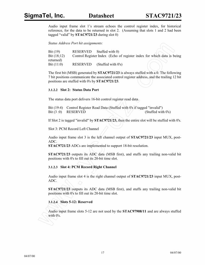
Audio input frame slot 1’s stream echoes the control register index, for historical reference, for the data to be returned in slot 2. (Assuming that slots 1 and 2 had been tagged “valid” by STAC9721/23 during slot 0) Status Address Port hit assignments: Bit (19) RESERVED Stuffed with 0) Bit (18;12) Control Register Index (Echo of register index for which data is being returned) Bit (11:0) RESERVED (Stuffed with 0's) The first bit (MSB) generated by STAC9721/23 is always stuffed with a 0. The following 7 bit positions communicate the associated control register address, and the trailing 12 bit positions are stuffed with 0's by STAC9721/23. 3.1.2.2 Slot 2: Status Data Port The status data port delivers 16-bit control register read data. Bit (19:4) Control Register Read Data (Stuffed with 0's if tagged "invalid") Bit (3 :0) RESERVED (Stuffed with 0's) If Slot 2 is tagged "invalid" by STAC9721/23, then the entire slot will be stuffed with 0's. Slot 3: PCM Record Left Channel Audio input frame slot 3 is the left channel output of STAC9721/23 input MUX, post-ADC. STAC9721/23 ADCs are implemented to support 18-bit resolution. STAC9721/23 outputs its ADC data (MSB first), and stuffs any trailing non-valid bit positions with 0's to fill out its 20-bit time slot. 3.1.2.3 Slot 4: PCM Record Right Channel Audio input frame slot 4 is the right channel output of STAC9721/23 input MUX, post-ADC. STAC9721/23 outputs its ADC data (MSB first), and stuffs any trailing non-valid bit positions with 0's to fill out its 20-bit time slot. 3.1.2.4 Slots 5-12: Reserved Audio input frame slots 5-12 are not used by the STAC97908/11 and are always stuffed with 0's.
www.yc-dz.com
SigmaTel, Inc. Datasheet STAC9721/23
18 04/07/00 04/07/00
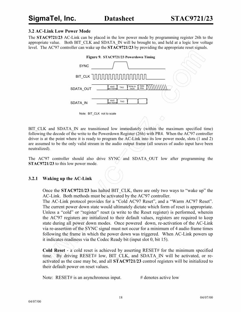
3.2 AC-Link Low Power Mode
The STAC9721/23 AC-Link can be placed in the low power mode by programming register 26h to the appropriate value. Both BIT_CLK and SDATA_IN will be brought to, and held at a logic low voltage level. The AC'97 controller can wake up the STAC9721/23 by providing the appropriate reset signals.
Figure 9. STAC9721/23 Powerdown Timing
SYNC
BIT_CLK
SDATA_OUT per frame
SDATA_IN
slot2 TAG Write to Data
slot2 TAGper frame
0x20 PR4
Note: BIT_CLK not to scale
BIT_CLK and SDATA_IN are transitioned low immediately (within the maximum specified time) following the decode of the write to the Powerdown Register (26h) with PR4. When the AC'97 controller driver is at the point where it is ready to program the AC-Link into its low power mode, slots (1 and 2) are assumed to be the only valid stream in the audio output frame (all sources of audio input have been neutralized). The AC'97 controller should also drive SYNC and SDATA_OUT low after programming the STAC9721/23 to this low power mode.
3.2.1 Waking up the AC-Link Once the STAC9721/23 has halted BIT_CLK, there are only two ways to “wake up” the AC-Link. Both methods must be activated by the AC'97 controller. The AC-Link protocol provides for a “Cold AC'97 Reset”, and a “Warm AC'97 Reset”. The current power down state would ultimately dictate which form of reset is appropriate. Unless a “cold” or “register” reset (a write to the Reset register) is performed, wherein the AC'97 registers are initialized to their default values, registers are required to keep state during all power down modes. Once powered down, re-activation of the AC-Link via re-assertion of the SYNC signal must not occur for a minimum of 4 audio frame times following the frame in which the power down was triggered. When AC-Link powers up it indicates readiness via the Codec Ready bit (input slot 0, bit 15). Cold Reset - a cold reset is achieved by asserting RESET# for the minimum specified time. By driving RESET# low, BIT_CLK, and SDATA_IN will be activated, or re-activated as the case may be, and all STAC9721/23 control registers will be initialized to their default power on reset values. Note: RESET# is an asynchronous input. # denotes active low
www.yc-dz.com
SigmaTel, Inc. Datasheet STAC9721/23
19 04/07/00 04/07/00
Warm Reset - a warm reset will re-activate the AC-Link without altering the current STAC9721/23 register values. A warm reset is signaled by driving SYNC high for a minimum of 1us in the absence of BIT_CLK. Note: Within normal audio frames, SYNC is a synchronous input. However, in the absence of BIT_CLK, SYNC is treated as an asynchronous input used in the generation of a warm reset to the STAC9721/23.
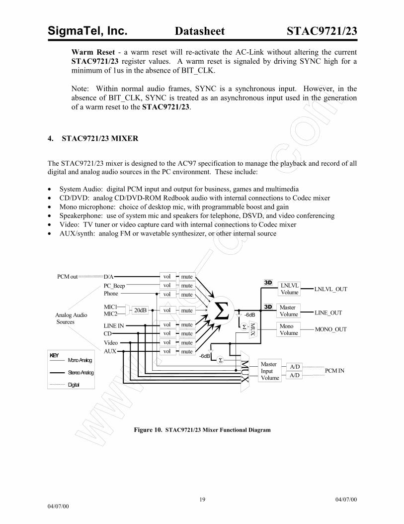
4. STAC9721/23 MIXER
The STAC9721/23 mixer is designed to the AC'97 specification to manage the playback and record of all digital and analog audio sources in the PC environment. These include: • System Audio: digital PCM input and output for business, games and multimedia • CD/DVD: analog CD/DVD-ROM Redbook audio with internal connections to Codec mixer • Mono microphone: choice of desktop mic, with programmable boost and gain • Speakerphone: use of system mic and speakers for telephone, DSVD, and video conferencing • Video: TV tuner or video capture card with internal connections to Codec mixer • AUX/synth: analog FM or wavetable synthesizer, or other internal source
Figure 10. STAC9721/23 Mixer Functional Diagram
vol mutePCM out D/A
Phone
LINE IN
LINE_OUT
CDVideoAUX
Analog Audio Sources
MONO_OUT
PCM IN
20dB MasterVolume
MonoVolume
A/DA/D
MasterInputVolume
Σ
Σ MU
XM
UX
volvol
vol
volvolvolvol
mutemute
mute
mutemutemutemute
KEYMono Analog
Stereo Analog
Digital
LNLVL_OUTLNLVLVolume
3D
3D-6dB
-6dB
PC_Beep
MIC1MIC2
Σ

www.yc-dz.com
SigmaTel, Inc. Datasheet STAC9721/23
20 04/07/00 04/07/00
Table 6. Mixer Functional Connections
Source Function Connection
PC_Beep PC beep pass thru from PC beeper output PHONE speakerphone or DLP in from telephony subsystem MIC1 desktop microphone from MIC jack MIC2 second microphone from second MIC jack
LINE_IN external audio source from line-in jack CD audio from CD-ROM cable from CD-ROM
VIDEO audio from TV tuner or video camera cable from TV or VidCap card AUX upgrade synth or other external source internal connector
PCM out digital audio output from AC'97 Controller AC-Link LINE_OUT stereo mix of all sources To output jack
LNLVL_OUT Additional stereo mix of all sources To output jack MONO_OUT MIC or mix for speakerphone or DLP out to telephony subsystem
PCM in digital audio input to AC'97 Controller AC-Link
4.1 Mixer Input The mixer provides recording and playback of any audio sources or output mix of all sources. The STAC9721/23 supports the following input sources: • any mono or stereo source • mono or stereo mix of all sources • 2-channel input w/mono output reference (mic + stereo mix) * Note: any unused input pins should be tied together and connected to ground with a capacitor (0.1 µF suggested), except the MIC1 and MIC2 inputs which require their own 0.1 µF capacitors to ground if not used.
4.2 Mixer Output The mixer generates two distinct outputs: • stereo mix of all sources for output to the LINE_OUT • stereo mix of all sources for output to the LNLVL_OUT • mono, MIC only or mix of all sources for MONO_OUT * Note: Mono output of stereo mix is attenuated by -6 dB to prevent clipping when left and right channels are combined.
4.3 PC Beep Implementation PC Beep is active on power up and defaults to an un-muted state. The user should mute this input before using any other mixer input because the PC Beep input can contribute noise to the LINE_OUT during normal operation.
www.yc-dz.com
SigmaTel, Inc. Datasheet STAC9721/23
21 04/07/00 04/07/00
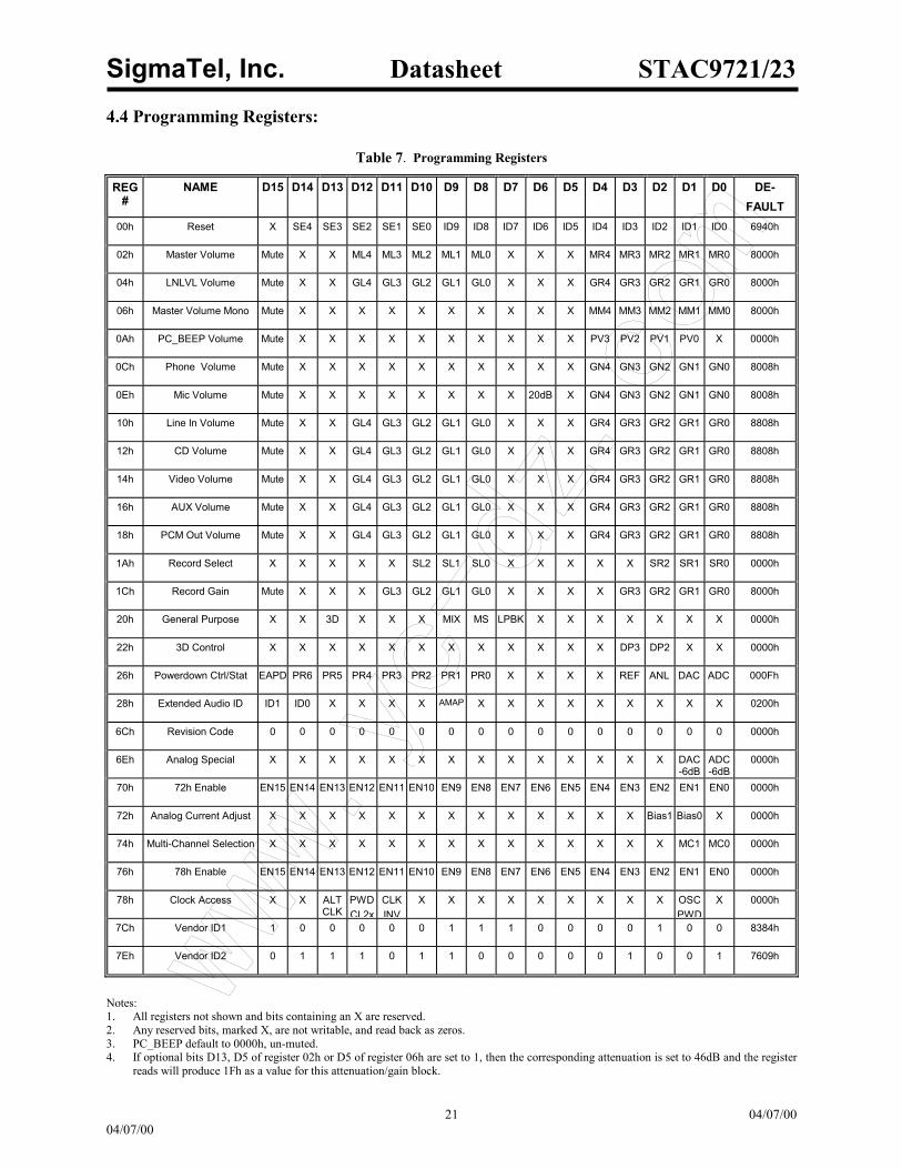
4.4 Programming Registers:
Table 7. Programming Registers
REG #
NAME D15 D14 D13 D12 D11 D10 D9 D8 D7 D6 D5 D4 D3 D2 D1 D0 DE- FAULT
00h Reset X SE4 SE3 SE2 SE1 SE0 ID9 ID8 ID7 ID6 ID5 ID4 ID3 ID2 ID1 ID0 6940h
02h Master Volume Mute X X ML4 ML3 ML2 ML1 ML0 X X X MR4 MR3 MR2 MR1 MR0 8000h
04h LNLVL Volume Mute X X GL4 GL3 GL2 GL1 GL0 X X X GR4 GR3 GR2 GR1 GR0 8000h
06h Master Volume Mono Mute X X X X X X X X X X MM4 MM3 MM2 MM1 MM0 8000h
0Ah PC_BEEP Volume Mute X X X X X X X X X X PV3 PV2 PV1 PV0 X 0000h
0Ch Phone Volume Mute X X X X X X X X X X GN4 GN3 GN2 GN1 GN0 8008h
0Eh Mic Volume Mute X X X X X X X X 20dB X GN4 GN3 GN2 GN1 GN0 8008h
10h Line In Volume Mute X X GL4 GL3 GL2 GL1 GL0 X X X GR4 GR3 GR2 GR1 GR0 8808h
12h CD Volume Mute X X GL4 GL3 GL2 GL1 GL0 X X X GR4 GR3 GR2 GR1 GR0 8808h
14h Video Volume Mute X X GL4 GL3 GL2 GL1 GL0 X X X GR4 GR3 GR2 GR1 GR0 8808h
16h AUX Volume Mute X X GL4 GL3 GL2 GL1 GL0 X X X GR4 GR3 GR2 GR1 GR0 8808h
18h PCM Out Volume Mute X X GL4 GL3 GL2 GL1 GL0 X X X GR4 GR3 GR2 GR1 GR0 8808h
1Ah Record Select X X X X X SL2 SL1 SL0 X X X X X SR2 SR1 SR0 0000h
1Ch Record Gain Mute X X X GL3 GL2 GL1 GL0 X X X X GR3 GR2 GR1 GR0 8000h
20h General Purpose X X 3D X X X MIX MS LPBK X X X X X X X 0000h
22h 3D Control X X X X X X X X X X X X DP3 DP2 X X 0000h
26h Powerdown Ctrl/Stat EAPD PR6 PR5 PR4 PR3 PR2 PR1 PR0 X X X X REF ANL DAC ADC 000Fh
28h Extended Audio ID ID1 ID0 X X X X AMAP X X X X X X X X X 0200h
6Ch Revision Code 0 0 0 0 0 0 0 0 0 0 0 0 0 0 0 0 0000h
6Eh Analog Special X X X X X X X X X X X X X X DAC -6dB
ADC -6dB
0000h
70h 72h Enable EN15 EN14 EN13 EN12 EN11 EN10 EN9 EN8 EN7 EN6 EN5 EN4 EN3 EN2 EN1 EN0 0000h
72h Analog Current Adjust X X X X X X X X X X X X X Bias1 Bias0 X 0000h
74h Multi-Channel Selection X X X X X X X X X X X X X X MC1 MC0 0000h
76h 78h Enable EN15 EN14 EN13 EN12 EN11 EN10 EN9 EN8 EN7 EN6 EN5 EN4 EN3 EN2 EN1 EN0 0000h
78h Clock Access X X ALT CLK
PWD CL2x
CLK INV
X X X X X X X X X OSC PWD
X 0000h
7Ch Vendor ID1 1 0 0 0 0 0 1 1 1 0 0 0 0 1 0 0 8384h
7Eh Vendor ID2 0 1 1 1 0 1 1 0 0 0 0 0 1 0 0 1 7609h
Notes: 1. All registers not shown and bits containing an X are reserved. 2. Any reserved bits, marked X, are not writable, and read back as zeros. 3. PC_BEEP default to 0000h, un-muted. 4. If optional bits D13, D5 of register 02h or D5 of register 06h are set to 1, then the corresponding attenuation is set to 46dB and the register
reads will produce 1Fh as a value for this attenuation/gain block.
www.yc-dz.com
SigmaTel, Inc. Datasheet STAC9721/23
22 04/07/00 04/07/00
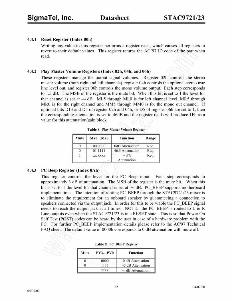
4.4.1 Reset Register (Index 00h) Writing any value to this register performs a register reset, which causes all registers to revert to their default values. This register returns the AC’97 ID code of the part when read.
4.4.2 Play Master Volume Registers (Index 02h, 04h, and 06h) These registers manage the output signal volumes. Register 02h controls the stereo master volume (both right and left channels), register 04h controls the optional stereo true line level out, and register 06h controls the mono volume output. Each step corresponds to 1.5 dB. The MSB of the register is the mute bit. When this bit is set to 1 the level for that channel is set at -∞ dB. ML5 through ML0 is for left channel level, MR5 through MR0 is for the right channel and MM5 through MM0 is for the mono out channel. If optional bits D13 and D5 of register 02h and 04h, or D5 of register 06h are set to 1, then the corresponding attenuation is set to 46dB and the register reads will produce 1Fh as a value for this attenuation/gain block
Table 8. Play Master Volume Register
Mute Mx5…Mx0 Function Range
0 00 0000 0dB Attenuation Req. 0 01 1111 46.5 Attenuation Req. 1 xx xxxx ∞ dB
Attenuation Req.
4.4.3 PC Beep Register (Index 0Ah) This register controls the level for the PC Beep input. Each step corresponds to approximately 3 dB of attenuation. The MSB of the register is the mute bit. When this bit is set to 1 the level for that channel is set at -∞ dB. PC_BEEP supports motherboard implementations. The intention of routing PC_BEEP through the STAC9721/23 mixer is to eliminate the requirement for an onboard speaker by guaranteeing a connection to speakers connected via the output jack. In order for this to be viable the PC_BEEP signal needs to reach the output jack at all times. NOTE: the PC_BEEP is routed to L & R Line outputs even when the STAC9721/23 is in a RESET state. This is so that Power On Self Test (POST) codes can be heard by the user in case of a hardware problem with the PC. For further PC_BEEP implementation details please refer to the AC'97 Technical FAQ sheet. The default value of 0000h corresponds to 0 dB attenuation with mute off.
Table 9. PC_BEEP Register
Mute PV3…PV0 Function
0 0000 0 dB Attenuation 0 1111 45 dB Attenuation 1 xxxx ∞ dB Attenuation
www.yc-dz.com
SigmaTel, Inc. Datasheet STAC9721/23
23 04/07/00 04/07/00
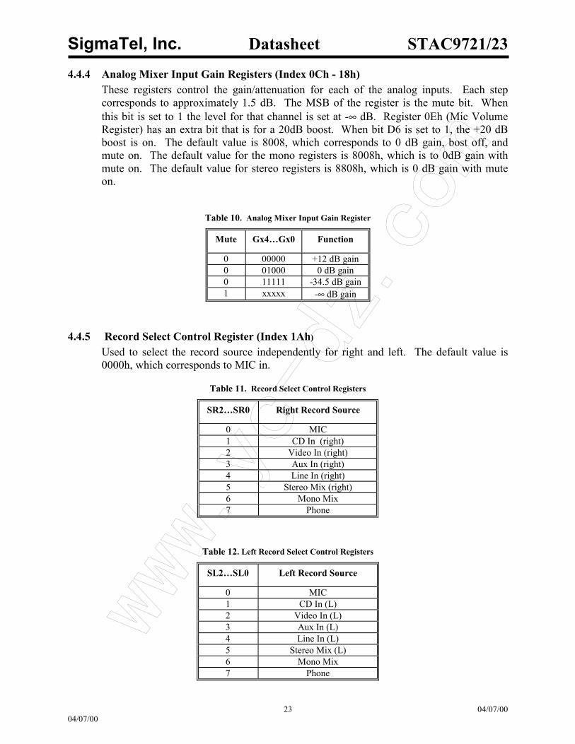
4.4.4 Analog Mixer Input Gain Registers (Index 0Ch - 18h) These registers control the gain/attenuation for each of the analog inputs. Each step corresponds to approximately 1.5 dB. The MSB of the register is the mute bit. When this bit is set to 1 the level for that channel is set at -∞ dB. Register 0Eh (Mic Volume Register) has an extra bit that is for a 20dB boost. When bit D6 is set to 1, the +20 dB boost is on. The default value is 8008, which corresponds to 0 dB gain, bost off, and mute on. The default value for the mono registers is 8008h, which is to 0dB gain with mute on. The default value for stereo registers is 8808h, which is 0 dB gain with mute on.
Table 10. Analog Mixer Input Gain Register
Mute Gx4…Gx0 Function
0 00000 +12 dB gain 0 01000 0 dB gain 0 11111 -34.5 dB gain 1 xxxxx -∞ dB gain
4.4.5 Record Select Control Register (Index 1Ah)
Used to select the record source independently for right and left. The default value is 0000h, which corresponds to MIC in.
Table 11. Record Select Control Registers
SR2…SR0 Right Record Source
0 MIC 1 CD In (right) 2 Video In (right) 3 Aux In (right) 4 Line In (right) 5 Stereo Mix (right) 6 Mono Mix 7 Phone
Table 12. Left Record Select Control Registers
SL2…SL0 Left Record Source
0 MIC 1 CD In (L) 2 Video In (L) 3 Aux In (L) 4 Line In (L) 5 Stereo Mix (L) 6 Mono Mix 7 Phone
www.yc-dz.com
SigmaTel, Inc. Datasheet STAC9721/23
24 04/07/00 04/07/00
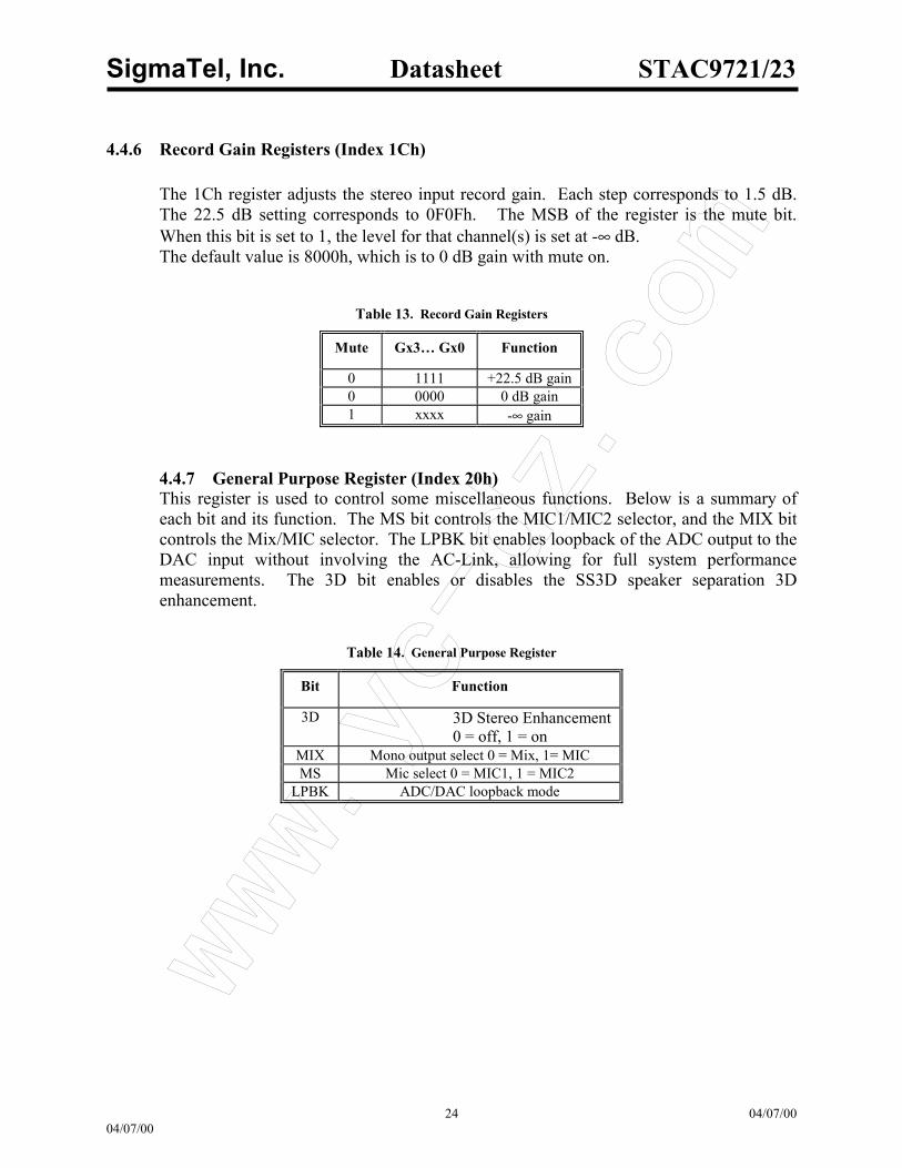
4.4.6 Record Gain Registers (Index 1Ch)
The 1Ch register adjusts the stereo input record gain. Each step corresponds to 1.5 dB. The 22.5 dB setting corresponds to 0F0Fh. The MSB of the register is the mute bit. When this bit is set to 1, the level for that channel(s) is set at -∞ dB. The default value is 8000h, which is to 0 dB gain with mute on.
Table 13. Record Gain Registers
Mute Gx3… Gx0 Function
0 1111 +22.5 dB gain 0 0000 0 dB gain 1 xxxx -∞ gain
4.4.7 General Purpose Register (Index 20h) This register is used to control some miscellaneous functions. Below is a summary of each bit and its function. The MS bit controls the MIC1/MIC2 selector, and the MIX bit controls the Mix/MIC selector. The LPBK bit enables loopback of the ADC output to the DAC input without involving the AC-Link, allowing for full system performance measurements. The 3D bit enables or disables the SS3D speaker separation 3D enhancement.
Table 14. General Purpose Register
Bit Function
3D 3D Stereo Enhancement 0 = off, 1 = on
MIX Mono output select 0 = Mix, 1= MIC MS Mic select 0 = MIC1, 1 = MIC2
LPBK ADC/DAC loopback mode
www.yc-dz.com
SigmaTel, Inc. Datasheet STAC9721/23
25 04/07/00 04/07/00
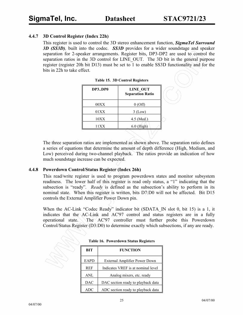
4.4.7 3D Control Register (Index 22h) This register is used to control the 3D stereo enhancement function, SigmaTel Surround 3D (SS3D), built into the codec. SS3D provides for a wider soundstage and speaker separation for 2-speaker arrangements. Register bits, DP3-DP2 are used to control the separation ratios in the 3D control for LINE_OUT. The 3D bit in the general purpose register (register 20h bit D13) must be set to 1 to enable SS3D functionality and for the bits in 22h to take effect.
Table 15. 3D Control Registers
DP3..DP0 LINE_OUT Separation Ratio
00XX 0 (Off)
01XX 3 (Low)
10XX 4.5 (Med.)
11XX 6.0 (High)
The three separation ratios are implemented as shown above. The separation ratio defines a series of equations that determine the amount of depth difference (High, Medium, and Low) perceived during two-channel playback. The ratios provide an indication of how much soundstage increase can be expected.
4.4.8 Powerdown Control/Status Register (Index 26h) This read/write register is used to program powerdown states and monitor subsystem readiness. The lower half of this register is read only status, a “1” indicating that the subsection is “ready”. Ready is defined as the subsection’s ability to perform in its nominal state. When this register is written, bits D7:D0 will not be affected. Bit D15 controls the External Amplifier Power Down pin. When the AC-Link “Codec Ready” indicator bit (SDATA_IN slot 0, bit 15) is a 1, it indicates that the AC-Link and AC'97 control and status registers are in a fully operational state. The AC'97 controller must further probe this Powerdown Control/Status Register (D3:D0) to determine exactly which subsections, if any are ready.
Table 16. Powerdown Status Registers
BIT FUNCTION
EAPD External Amplifier Power Down
REF Indicates VREF is at nominal level
ANL Analog mixers, etc. ready
DAC DAC section ready to playback data
ADC ADC section ready to playback data
www.yc-dz.com
SigmaTel, Inc. Datasheet STAC9721/23
26 04/07/00 04/07/00
4.4.8.1 External Amplifier Power Down Control The EAPD bit D15 of the Powerdown Control/Status Register (Index 26h) directly controls the output of the EAPD output, pin 45, and produces a logical “1” when this bit is set to logic high. This function is used to control an external audio amplifier power down. EAPD = 0 places approximately 0V on the output pin, enabling an external audio amplifier. EAPD = 1 places approximately DVDD on the output pin, disabling the external audio amplifier. Audio amplifiers that operate with reverse polarity will likely require an external inverter to maintain software driver compatibility.Extended Audio ID Register (Index 28)
4.4.9 Extended Audio Register (Index 28h) The Extended Audio ID register is a read only register. ID1 and ID0 echo the configuration of the codec as defined by the programming of pins 45 and 46 externally. “00” returned defines the codec as the primary codec, while any other code identifies the codec as one of three secondary codec possibilities. The AMAP bit, D9, will return a 1 indicating that the codec supports the optional “AC’97 2.1 compliant AC-link slot to audio DAC mappings”. The default condition assumes that 0, 0 are loaded in the MC1 and MC0 bits of the Multi-Channel Programming Register (Index 74h). With 0s in the MCx bits, the codec slot assignments are as per the AC’97 specification recommendations. If the MCx bits do not contain 0s, the slot assignments are as per the table in the section describing the Multi-Channel Programming Register (Index 74h).
Table 17. Extended Audio ID Register Functions
BIT FUNCTION
IDx External CID pin status
AMAP Multi-channel slot support
4.4.10 Revision (Index 6Ch) The device Revision register (index 6Ch) contains a software readable revision-specific code used to identify performance, architectural, or software differences between various device revisions. Bits 7:0 of the Revision register are user readable; bits 15:8 are not used at this time and will return zeros when read. The lower order bits of the Revision Register (bits 7:0) are currently set to 00h, and will likely change if there are any STAC9721/23 metal revisions.
4.4.11 Analog Special Register (Index 6Eh) The Analog Special Register has two read/write bits used to control two functions specific to the STAC9721/23. DAC –6dB is used to program the DAC outputs to a –6dB signal level relative to the value of gain already programmed. Similarly, ADC –6dB attenuates any signal input to the ADC by 6dB.
www.yc-dz.com
SigmaTel, Inc. Datasheet STAC9721/23
27 04/07/00 04/07/00
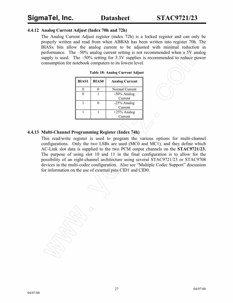
4.4.12 Analog Current Adjust (Index 70h and 72h) The Analog Current Adjust register (index 72h) is a locked register and can only be properly written and read from when ABBAh has been written into register 70h. The BIASx bits allow the analog current to be adjusted with minimal reduction in performance. The –50% analog current setting is not recommended when a 5V analog supply is used. The –50% setting for 3.3V supplies is recommended to reduce power consumption for notebook computers to its lowest level.
Table 18: Analog Current Adjust
BIAS1 BIAS0 Analog Current
0 0 Normal Current 0 1 -50% Analog
Current 1 0 -25% Analog
Current 1 1 +25% Analog
Current
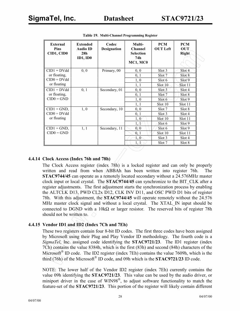
4.4.13 Multi-Channel Programming Register (Index 74h) This read/write register is used to program the various options for multi-channel configurations. Only the two LSBs are used (MC0 and MC1), and they define which AC-Link slot data is supplied to the two PCM output channels on the STAC9721/23. The purpose of using slot 10 and 11 in the final configuration is to allow for the possibility of an eight-channel architecture using several STAC9721/23 or STAC9708 devices in the multi-codec configuration. Also see “Multiple Codec Support” discussion for information on the use of external pins CID1 and CID0.
www.yc-dz.com
SigmaTel, Inc. Datasheet STAC9721/23
28 04/07/00 04/07/00
Table 19. Multi-Channel Programming Register
External Pins
CID1, CID0
Extended Audio ID
28h ID1, ID0
Codec Designation
Multi-Channel Selection
74h MC1, MC0
PCM OUT Left
PCM OUT Right
0, 0 Slot 3 Slot 4 0, 1 Slot 7 Slot 8 1, 0 Slot 6 Slot 9
CID1 = DVdd or floating,
CID0 = DVdd or floating
0, 0 Primary, 00
1, 1 Slot 10 Slot 11 0, 0 Slot 3 Slot 4 0, 1 Slot 7 Slot 8 1, 0 Slot 6 Slot 9
CID1 = DVdd or floating,
CID0 = GND
0, 1 Secondary, 01
1, 1 Slot 10 Slot 11 0, 0 Slot 7 Slot 8 0, 1 Slot 3 Slot 4 1, 0 Slot 10 Slot 11
CID1 = GND, CID0 = DVdd
or floating
1, 0 Secondary, 10
1, 1 Slot 6 Slot 9 0, 0 Slot 6 Slot 9 0, 1 Slot 10 Slot 11 1, 0 Slot 3 Slot 4
CID1 = GND, CID0 = GND
1, 1 Secondary, 11
1, 1 Slot 7 Slot 8
4.4.14 Clock Access (Index 76h and 78h) The Clock Access register (index 78h) is a locked register and can only be properly written and read from when ABBAh has been written into register 76h. The STAC9744/45 can operate as a remotely located secondary without a 24.576MHz master clock input or local crystal. The STAC9744/45 can synchronize to the BIT_CLK after a register adjustments. The first adjustment starts the synchronization process by enabling the ALTCLK D13, PWD CL2x D12, CLK INV D11, and OSC PWD D1 bits of register 78h. With this adjustment, the STAC9744/45 will operate remotely without the 24.576 MHz master clock signal and without a local crystal. The XTAL_IN input should be connected to DGND with a 10kΩ or larger resistor. The reserved bits of register 78h should not be written to.
4.4.15 Vendor ID1 and ID2 (Index 7Ch and 7Eh) These two registers contain four 8-bit ID codes. The first three codes have been assigned by Microsoft using their Plug and Play Vendor ID methodology. The fourth code is a SigmaTel, Inc. assigned code identifying the STAC9721/23. The ID1 register (index 7Ch) contains the value 8384h, which is the first (83h) and second (84h) characters of the Microsoft ID code. The ID2 register (index 7Eh) contains the value 7609h, which is the third (76h) of the Microsoft ID code, and 09h which is the STAC9721/23 ID code. NOTE: The lower half of the Vendor ID2 register (index 7Eh) currently contains the value 09h identifying the STAC9721/23. This value can be used by the audio driver, or miniport driver in the case of WIN98, to adjust software functionality to match the feature-set of the STAC9721/23. This portion of the register will likely contain different
www.yc-dz.com
SigmaTel, Inc. Datasheet STAC9721/23
29 04/07/00 04/07/00
values if the software profile of the STAC9721/23 changes, as in the case of silicon level device modifications. This will allow the software driver to identify any required operational differences between the existing STAC9721/23 and any future versions.
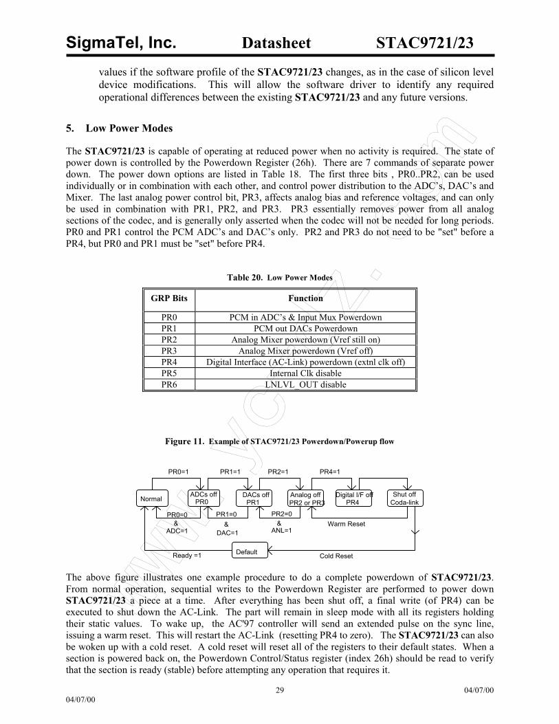
5. Low Power Modes
The STAC9721/23 is capable of operating at reduced power when no activity is required. The state of power down is controlled by the Powerdown Register (26h). There are 7 commands of separate power down. The power down options are listed in Table 18. The first three bits , PR0..PR2, can be used individually or in combination with each other, and control power distribution to the ADC’s, DAC’s and Mixer. The last analog power control bit, PR3, affects analog bias and reference voltages, and can only be used in combination with PR1, PR2, and PR3. PR3 essentially removes power from all analog sections of the codec, and is generally only asserted when the codec will not be needed for long periods. PR0 and PR1 control the PCM ADC’s and DAC’s only. PR2 and PR3 do not need to be "set" before a PR4, but PR0 and PR1 must be "set" before PR4.
Table 20. Low Power Modes
GRP Bits Function
PR0 PCM in ADC’s & Input Mux Powerdown PR1 PCM out DACs Powerdown PR2 Analog Mixer powerdown (Vref still on) PR3 Analog Mixer powerdown (Vref off) PR4 Digital Interface (AC-Link) powerdown (extnl clk off) PR5 Internal Clk disable PR6 LNLVL_OUT disable
Figure 11. Example of STAC9721/23 Powerdown/Powerup flow
PR0=1 PR1=1 PR2=1 PR4=1
Default
Normal ADCs offPR0
DACs offPR1
Analog offPR2 or PR3
Digital I/F offPR4
Shut offCoda-link
PR0=0&
ADC=1
PR1=0&
DAC=1
PR2=0&
ANL=1Warm Reset
Cold ResetReady =1 The above figure illustrates one example procedure to do a complete powerdown of STAC9721/23. From normal operation, sequential writes to the Powerdown Register are performed to power down STAC9721/23 a piece at a time. After everything has been shut off, a final write (of PR4) can be executed to shut down the AC-Link. The part will remain in sleep mode with all its registers holding their static values. To wake up, the AC'97 controller will send an extended pulse on the sync line, issuing a warm reset. This will restart the AC-Link (resetting PR4 to zero). The STAC9721/23 can also be woken up with a cold reset. A cold reset will reset all of the registers to their default states. When a section is powered back on, the Powerdown Control/Status register (index 26h) should be read to verify that the section is ready (stable) before attempting any operation that requires it.
www.yc-dz.com
SigmaTel, Inc. Datasheet STAC9721/23
30 04/07/00 04/07/00
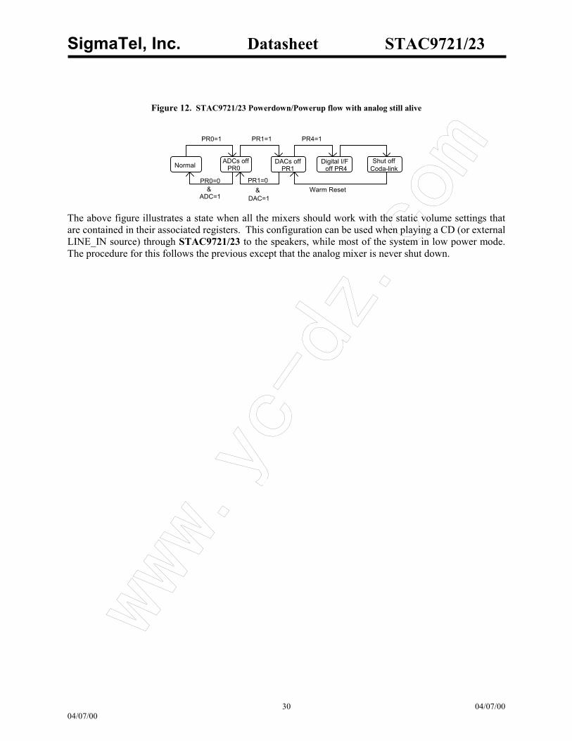
Figure 12. STAC9721/23 Powerdown/Powerup flow with analog still alive
PR0=1 PR1=1 PR4=1
Normal ADCs offPR0
DACs offPR1
Digital I/F off PR4
Shut offCoda-link
PR0=0&
ADC=1
PR1=0&
DAC=1Warm Reset
The above figure illustrates a state when all the mixers should work with the static volume settings that are contained in their associated registers. This configuration can be used when playing a CD (or external LINE_IN source) through STAC9721/23 to the speakers, while most of the system in low power mode. The procedure for this follows the previous except that the analog mixer is never shut down.
www.yc-dz.com
SigmaTel, Inc. Datasheet STAC9721/23
31 04/07/00 04/07/00
6. MULTIPLE CODEC SUPPORT
The STAC9721/23 provides support for the multi-codec option according to the Intel AC'97, rev 2.1 specification. By definition there can be only one Primary Codec (Codec ID 00) and up to three Secondary Codecs (Codec IDs 01,10, and 11). The Codec ID functions as a chip select. Secondary devices therefore have completely orthogonal register sets; each is individually accessible and they do not share registers.
6.1 Primary/Secondary Codec Selection In a multi-codec environment the codec ID is provided by external programming of pins 45 and 46 (CID0 and CID1). The CID pin electrical function is logically inverted from the codec ID designation. The corresponding pin state and its associated codec ID are listed in the "Codec ID Selection" table. Also see slot assignment discussion, “Multi-Channel Programming Register (Index 74)”.
Table 21. Codec ID Selection
CID1 State CID0 State Codec ID Codec Status EXTENDED AUDIO ID, 28h
ID1, ID0
+5V or floating +5V or floating 00 Primary 0, 0 +5V or floating 0V 01 Secondary 0, 1
0V +5V or floating 10 Secondary 1, 0 0V 0V 11 Secondary 1, 1
6.1.1 Primary Codec Operation As a Primary device the STAC9721/23 is completely compatible with existing AC'97 definitions and extensions. Primary Codec registers are accessed exactly as defined in the AC'97 Component Specification and AC'97 Extensions. The STAC9721/23 operates as Primary by default, and the external ID pins (47 and 48) have internal pull-ups so that these pins may be left as no-connects for primary operation. When used as the Primary Codec, the STAC9721/23 generates the master AC-Link BIT_CLK for both the AC'97 Digital Controller and any Secondary Codecs. The STAC9721/23 can support up to 4, 10 KΩ 50 pF loads on the BIT_CLK. This is to insure that up to 4 Codec implementations will not load down the clock output.
6.1.2 Secondary Codec Operation When the STAC9721/23 is configured as a Secondary device the BIT_CLK pin is configured as an input at power up. Using the BIT_CLK provided by the Primary Codec insures that everything on the AC-Link will be synchronous. As a Secondary device it can be defined as Codec ID 01, 10, or 11 in the two-bit field(s) of the Extended Audio and/or Extended Modem ID Register(s).
www.yc-dz.com
SigmaTel, Inc. Datasheet STAC9721/23
32 04/07/00 04/07/00
6.2 Secondary Codec Register Access Definitions The AC'97 Digital Controller can independently access Primary and Secondary Codec registers by using a 2-bit Codec ID field (chip select) which is defined as the LSBs of Output Slot 0. For Secondary Codec access, the AC'97 Digital Controller must invalidate the tag bits for Slot 1 and 2 Command Address and Data (Slot 0, bits 14 and 13) and place a non-zero value (01, 10, or 11) into the Codec ID field (Slot 0, bits 1 and 0). As a Secondary Codec, the STAC9721/23 will disregard the Command Address and Command Data (Slot 0, bits 14 and 13) tag bits when it sees a 2-bit Codec ID value (Slot 0, bits 1 and 0) that matches its configuration. In a sense the Secondary Codec ID field functions as an alternative Valid Command Address (for Secondary reads and writes) and Command Data (for Secondary writes) tag indicator. Secondary Codecs must monitor the Frame Valid bit, and ignore the frame (regardless of the state of the Secondary Codec ID bits) if it is not valid. AC'97 Digital Controllers should set the frame valid bit for a frame with a secondary register access, even if no other bits in the output tag slot except the Secondary Codec ID bits are set. This method is designed to be backward compatible with existing AC'97 controllers and Codecs. There is no change to output Slot 1 or 2 definitions.
Table 22. Secondary Codec Register Access Slot 0 Bit Definitions
Output Tag Slot (16-bits)
Bit Description 15 Frame Valid 14 Slot 1 Valid Command Address bit (†Primary Codec only) 13 Slot 2 Valid Command Data bit (†Primary Codec only)
12-3 Slot 3-12 Valid bits as defined by AC'97 2 Reserved (Set to “0”)
†1-0 2-bit Codec ID field (00 reserved for Primary; 01, 10, 11 indicate Secondary) † New definitions for Secondary Codec Register Access
7. TESTABILITY
The STAC9721/23 has two test modes. One is for ATE in-circuit test and the other is restricted for SigmaTel’s internal use. STAC9721/23 enters the ATE in circuit test mode if SDATA_OUT is sampled high at the trailing edge of RESET#. Once in the ATE test mode, the digital AC-Link outputs (BIT_CLK and SDATA_IN) are driven to a high impedance state. This allows ATE in-circuit testing of the AC'97 controller. This case will never occur during standard operating conditions. Once either of the two test modes have been entered, the STAC9704/7 must be issued another rest with all AC-link signals held low to return to the normal operating mode.
www.yc-dz.com
SigmaTel, Inc. Datasheet STAC9721/23
33 04/07/00 04/07/00
8. EXTENDED CODEC FUNCTIONALITY
8.1 Anti-Pop Circuitry The STAC9721/23 provides an integrated output signal (APOP on pin 34) to aid in low-component-count anti-pop implementations. An audible speaker "pop" can occur when the main power is applied to, or removed from, the codec or audio output amplifier. In ac coupled systems, the speaker sided of the ac coupling capacitor is shunted to ground through a transistor or FET; this prevents audible pops when the system is powering on and off. A 10 µF capacitor on CAP1 provides a delay to hold-off power to the output stages on power up. A 22 µF capacitor provides reserve power to sustain the output shunting action until the power has been fully removed on power down. APOP is active logic high during shunting operations; APOP is at logic low during normal operations.
9. AC TIMING CHARACTERISTICS (Tambient = 25 °C, AVdd = DVdd = 5.0V or 3.3V ± 5%, AVss=DVss+0V; 50pF external load)
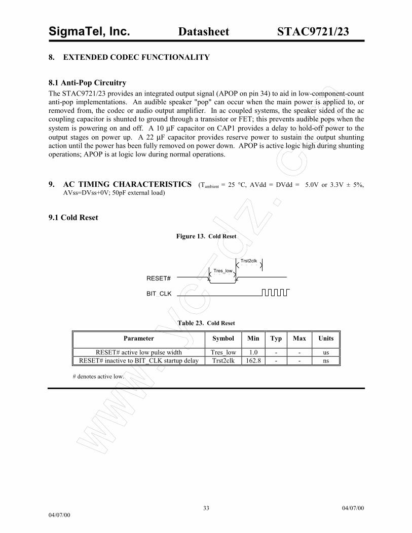
9.1 Cold Reset
Figure 13. Cold Reset
RESET#
BIT_CLK
Tres_low
Trst2clk
Table 23. Cold Reset
Parameter Symbol Min Typ Max Units
RESET# active low pulse width Tres_low 1.0 - - us RESET# inactive to BIT_CLK startup delay Trst2clk 162.8 - - ns
# denotes active low.
www.yc-dz.com
SigmaTel, Inc. Datasheet STAC9721/23
34 04/07/00 04/07/00
9.2 Warm Reset
Figure 14. Warm Reset
SYNC
BIT_CLK
Tsync_2clkTsync_high
Table 24. Warm Reset
Parameter Symbol Min Typ Max Units
SYNC active high pulse width Tsync_high 1.0 1.3 - us SYNC inactive to BIT_CLK startup delay Tsync2clk 162.8 - - ns
9.3 Clocks
Figure 15. Clocks
BIT_CLK
SYNC
Tclk_high
Tclk_low
Tclk_period
Tsync_low
Tsync_high
Tsync_period
Table 25. Clocks
Parameter Symbol Min Typ Max Units
BIT_CLK frequency - 12.288 - MHz BIT_CLK period Tclk_period - 81.4 - ns
BIT_CLK output jitter - - 750 ps BLT_CLK high pulsewidth (note 1) Tclk_high 36 40.7 45 ns BIT_CLK low pulse width (note 1) Tclk_low 36 40.7 45 ns
SYNC frequency - 48.0 - kHz SYNC period Tsync_period - 20.8 - us
SYNC high pulse width Tsync_high - 1.3 - us SYNC low_pulse width Tsync_low - 19.5 - us
Notes: 1) Worst case duty cycle restricted to 40/60.
www.yc-dz.com
SigmaTel, Inc. Datasheet STAC9721/23
35 04/07/00 04/07/00
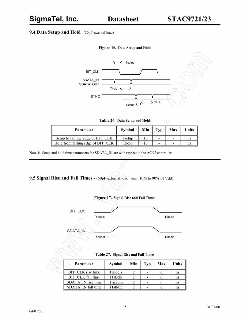
9.4 Data Setup and Hold (50pF external load)
Figure 16. Data Setup and Hold
BIT_CLK
SDATA_INSDATA_OUT
SYNC
Tsetup
Thold
TsetupThold
Table 26. Data Setup and Hold
Parameter Symbol Min Typ Max Units
Setup to falling edge of BIT_CLK Tsetup 10 - - ns Hold from falling edge of BIT_CLK Thold 10 - - ns
Note 1: Setup and hold time parameters for SDATA_IN are with respect to the AC'97 controller.
9.5 Signal Rise and Fall Times - (50pF external load; from 10% to 90% of Vdd)
Figure 17. Signal Rise and Fall Times
BIT_CLK
SDATA_IN
Triseclk Tfallclk
Trisedin Tfalldin
Table 27. Signal Rise and Fall Times
Parameter Symbol Min Typ Max Units
BIT_CLK rise time Triseclk 2 - 6 ns BIT_CLK fall time Tfallclk 2 - 6 ns
SDATA_IN rise time Trisedin 2 - 6 ns SDATA_IN fall time Tfalldin 2 - 6 ns
www.yc-dz.com
SigmaTel, Inc. Datasheet STAC9721/23
36 04/07/00 04/07/00
9.6 AC-Link Low Power Mode Timing
Figure 18. AC-Link Low Power Mode Timing
SYNC
BIT_CLK
SDATA_OUT
SDATA_IN
Don't care
Slot 1 Slot 2
Write to Data0x20 PR4
Note: BIT_CLK not to scale
Ts2_pdown
Table 28. AC-Link Low Power Mode Timing
Parameter Symbol Min Typ Max Units
End of Slot 2 to BIT_CLK, SDATA_IN low Ts2_pdown - - 1.0 us
www.yc-dz.com
SigmaTel, Inc. Datasheet STAC9721/23
37 04/07/00 04/07/00
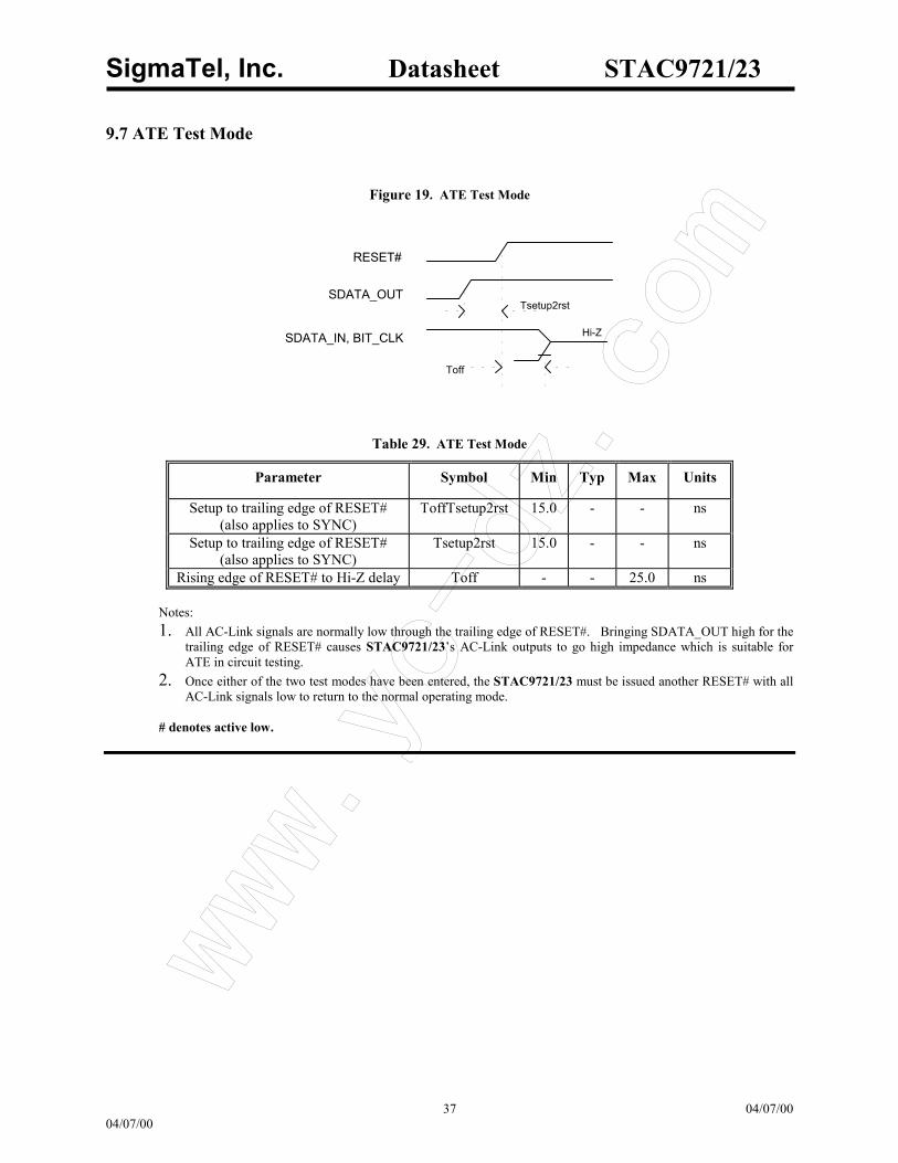
9.7 ATE Test Mode
Figure 19. ATE Test Mode
RESET#
SDATA_OUT
SDATA_IN, BIT_CLK
Toff
Hi-Z
Tsetup2rst
Table 29. ATE Test Mode
Parameter Symbol Min Typ Max Units
Setup to trailing edge of RESET# (also applies to SYNC)
ToffTsetup2rst 15.0 - - ns
Setup to trailing edge of RESET# (also applies to SYNC)
Tsetup2rst 15.0 - - ns
Rising edge of RESET# to Hi-Z delay Toff - - 25.0 ns Notes:
1. All AC-Link signals are normally low through the trailing edge of RESET#. Bringing SDATA_OUT high for the trailing edge of RESET# causes STAC9721/23’s AC-Link outputs to go high impedance which is suitable for ATE in circuit testing.
2. Once either of the two test modes have been entered, the STAC9721/23 must be issued another RESET# with all AC-Link signals low to return to the normal operating mode.
# denotes active low.
www.yc-dz.com
SigmaTel, Inc. Datasheet STAC9721/23
38 04/07/00 04/07/00
10. ELECTRICAL SPECIFICATIONS:
10.1 Absolute Maximum Ratings:
Voltage on any pin relative to Ground Vss - 0.3V TO Vdd + 0.3V Operating Temperature 0 oC
TO 70 o
C
Storage Temperature -55 oC TO +125 o
C
Soldering Temperature 260 oC FOR 10 SECONDS
Output Current per Pin ± 4 mA except Vrefout = ± 5mA
10.2 Recommended Operating Conditions
Table 30. Operating Conditions
PARAMETER MIN TYP MAX UNITS
Power Supplies + 3.3V Digital + 5V Digital + 5V Analog + 3.3V Analog
3.135 4.75 4.75
3.135
3.3 5 5
3.3
3.465 5.25 5.25
3.465
V V V V
Ambient Temperature 0 - 70 oC
SigmaTel reserves the right to change specifications without notice.
www.yc-dz.com
SigmaTel, Inc. Datasheet STAC9721/23
39 04/07/00 04/07/00
10.3 Power Consumption
Table 31: Power Consumption at Default Analog Current
PARAMETER MIN TYP MAX UNITS
Digital Supply Current + 5V Digital: DAC and ADC Active + 3.3V Digital: DAC and ADC Active + 3.3V Digital: DAC and ADC Muted
30 20 7
mA mA mA
Analog Supply Current + 5V Analog: PC_BEEP Muted + 3.3V Analog: PC_BEEP Muted
38 34
mA mA
Power Down Status PR0 +5V Analog Supply Current PR1 +5V Analog Supply Current PR2 +5V Analog Supply Current PR3 +5V Analog Supply Current PR0,1,2,3 +5V Analog Supply Current PR4 +3.3V Digital Supply Current PR4 +5V Digital Supply Current PR5 No Effect
28 37 28 1.1 0.6 0.1 0.1
mA mA mA mA mA mA mA
Table 32: Power Consumption at 3.3V Analog, Low Current Mode*
PARAMETER MIN TYP MAX UNITS
Digital Supply Current + 3.3V Digital with DAC and ADC Active
20
mA
Analog Supply Current + 3.3V Analog with DAC and ADC Muted
19
mA
Power Down Status PR0 +3.3V Analog Supply Current PR1 +3.3V Analog Supply Current PR2 +3.3V Analog Supply Current PR3 +3.3V Analog Supply Current PR0,1,2,3 +3.3V Analog Supply Current PR4 +3.3V Digital Supply Current PR5 No Effect
15 19 15 0.4 0.4 0.1
mA mA mA mA mA mA
* -50% Analog Current Setting (Recommended for 3.3V Analog only): Register 70h=ABBAh, 72h=0002h
www.yc-dz.com
SigmaTel, Inc. Datasheet STAC9721/23
40 04/07/00 04/07/00
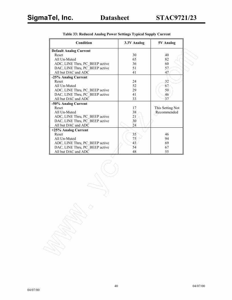
Table 33: Reduced Analog Power Settings Typical Supply Current
Condition 3.3V Analog 5V Analog
Default Analog Current Reset All Un-Muted ADC, LINE Thru, PC_BEEP active DAC, LINE Thru, PC_BEEP active All but DAC and ADC
30 65 36 51 41
40 82 60 57 47
-25% Analog Current Reset All Un-Muted ADC, LINE Thru, PC_BEEP active DAC, LINE Thru, PC_BEEP active All but DAC and ADC
24 52 29 41 33
32 67 50 46 37
-50% Analog Current Reset All Un-Muted ADC, LINE Thru, PC_BEEP active DAC, LINE Thru, PC_BEEP active All but DAC and ADC
17 38 21 30 24
This Setting Not Recommended
+25% Analog Current Reset All Un-Muted ADC, LINE Thru, PC_BEEP active DAC, LINE Thru, PC_BEEP active All but DAC and ADC
35 75 43 54 48
46 94 69 67 55
www.yc-dz.com
SigmaTel, Inc. Datasheet STAC9721/23
41 04/07/00 04/07/00
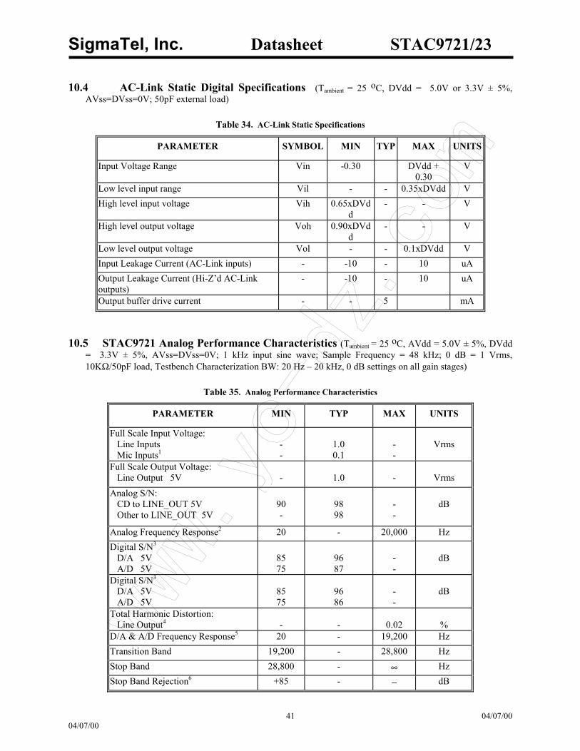
10.4 AC-Link Static Digital Specifications (Tambient = 25 oC, DVdd = 5.0V or 3.3V ± 5%, AVss=DVss=0V; 50pF external load)
Table 34. AC-Link Static Specifications
PARAMETER SYMBOL MIN TYP MAX UNITS
Input Voltage Range Vin -0.30 DVdd + 0.30
V
Low level input range Vil - - 0.35xDVdd V High level input voltage Vih 0.65xDVd
d - - V
High level output voltage Voh 0.90xDVdd
- - V
Low level output voltage Vol - - 0.1xDVdd V Input Leakage Current (AC-Link inputs) - -10 - 10 uA Output Leakage Current (Hi-Z’d AC-Link outputs)
- -10 - 10 uA
Output buffer drive current - - 5 mA
10.5 STAC9721 Analog Performance Characteristics (Tambient = 25 oC, AVdd = 5.0V ± 5%, DVdd = 3.3V ± 5%, AVss=DVss=0V; 1 kHz input sine wave; Sample Frequency = 48 kHz; 0 dB = 1 Vrms, 10KΩ/50pF load, Testbench Characterization BW: 20 Hz – 20 kHz, 0 dB settings on all gain stages)
Table 35. Analog Performance Characteristics
PARAMETER MIN TYP MAX UNITS
Full Scale Input Voltage: Line Inputs Mic Inputs1
- -
1.0 0.1
- -
Vrms
Full Scale Output Voltage: Line Output 5V
-
1.0
-
Vrms
Analog S/N: CD to LINE_OUT 5V Other to LINE_OUT 5V
90 -
98 98
- -
dB
Analog Frequency Response2 20 - 20,000 Hz Digital S/N3 D/A 5V A/D 5V
85 75
96 87
- -
dB
Digital S/N3 D/A 5V A/D 5V
85 75
96 86
- -
dB
Total Harmonic Distortion: Line Output4
-
-
0.02
%
D/A & A/D Frequency Response5 20 - 19,200 Hz Transition Band 19,200 - 28,800 Hz Stop Band 28,800 - ∞ Hz Stop Band Rejection6 +85 - − dB
www.yc-dz.com
SigmaTel, Inc. Datasheet STAC9721/23
42 04/07/00 04/07/00
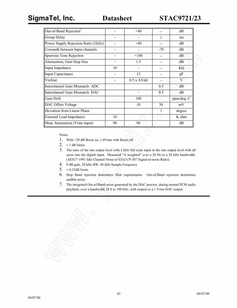
Out-of-Band Rejection7 - +40 − dB Group Delay - - 1 ms Power Supply Rejection Ratio (1kHz) - +40 − dB Crosstalk between Input channels - - -70 dB Spurious Tone Rejection - +100 − dB Attenuation, Gain Step Size - 1.5 − dB Input Impedance 10 - − KΩ Input Capacitance - 15 − pF Vrefout - 0.5 x AVdd − V Interchannel Gain Mismatch ADC 0.5 dB Interchannel Gain Mismatch DAC - 0.5 dB Gain Drift 100 ppm/deg. C DAC Offset Voltage 10 50 mV Deviation from Linear Phase 1 degree External Load Impedance 10 K ohm Mute Attenuation (Vrms input) 90 96 dB
Notes: 1. With +20 dB Boost on, 1.0Vrms with Boost off 2. ± 1 dB limits 3. The ratio of the rms output level with 1 kHz full scale input to the rms output level with all
zeros into the digital input. Measured “A weighted” over a 20 Hz to a 20 kHz bandwidth. (AES17-1991 Idle Channel Noise or EIAJ CP-307 Signal-to-noise Ratio).
4. 0 dB gain, 20 kHz BW, 48 kHz Sample Frequency 5. ± 0.25dB limits 6. Stop Band rejection determines filter requirements. Out-of-Band rejection determines
audible noise. 7. The integrated Out-of-Band noise generated by the DAC process, during normal PCM audio
playback, over a bandwidth 28.8 to 100 kHz, with respect to a 1 Vrms DAC output.
www.yc-dz.com
SigmaTel, Inc. Datasheet STAC9721/23
43 04/07/00 04/07/00
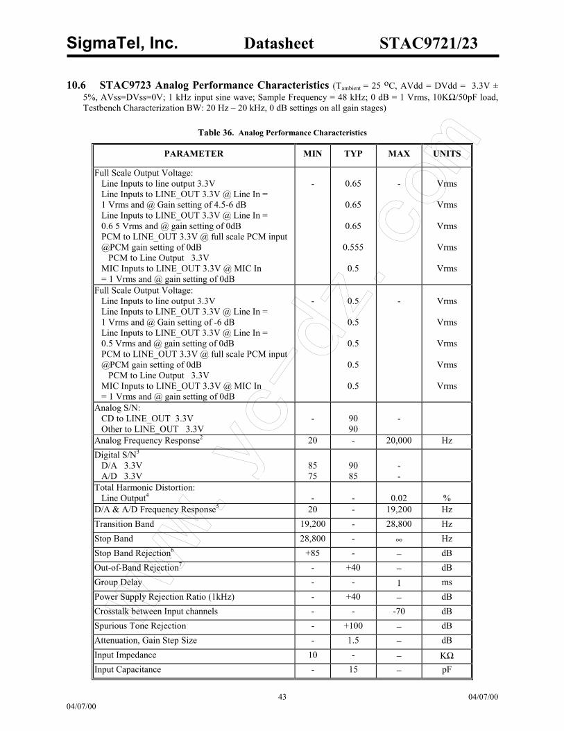
10.6 STAC9723 Analog Performance Characteristics (Tambient = 25 oC, AVdd = DVdd = 3.3V ± 5%, AVss=DVss=0V; 1 kHz input sine wave; Sample Frequency = 48 kHz; 0 dB = 1 Vrms, 10KΩ/50pF load, Testbench Characterization BW: 20 Hz – 20 kHz, 0 dB settings on all gain stages)
Table 36. Analog Performance Characteristics
PARAMETER MIN TYP MAX UNITS
Full Scale Output Voltage: Line Inputs to line output 3.3V Line Inputs to LINE_OUT 3.3V @ Line In = 1 Vrms and @ Gain setting of 4.5-6 dB Line Inputs to LINE_OUT 3.3V @ Line In = 0.6 5 Vrms and @ gain setting of 0dB PCM to LINE_OUT 3.3V @ full scale PCM input @PCM gain setting of 0dB PCM to Line Output 3.3V MIC Inputs to LINE_OUT 3.3V @ MIC In = 1 Vrms and @ gain setting of 0dB
-
0.65
0.65
0.65
0.555
0.5
-
Vrms
Vrms
Vrms
Vrms
Vrms
Full Scale Output Voltage: Line Inputs to line output 3.3V Line Inputs to LINE_OUT 3.3V @ Line In = 1 Vrms and @ Gain setting of -6 dB Line Inputs to LINE_OUT 3.3V @ Line In = 0.5 Vrms and @ gain setting of 0dB PCM to LINE_OUT 3.3V @ full scale PCM input @PCM gain setting of 0dB PCM to Line Output 3.3V MIC Inputs to LINE_OUT 3.3V @ MIC In = 1 Vrms and @ gain setting of 0dB
-
0.5
0.5
0.5
0.5
0.5
-
Vrms
Vrms
Vrms
Vrms
Vrms
Analog S/N: CD to LINE_OUT 3.3V Other to LINE_OUT 3.3V
-
90 90
-
Analog Frequency Response2 20 - 20,000 Hz Digital S/N3 D/A 3.3V A/D 3.3V
85 75
90 85
- -
Total Harmonic Distortion: Line Output4
-
-
0.02
%
D/A & A/D Frequency Response5 20 - 19,200 Hz Transition Band 19,200 - 28,800 Hz Stop Band 28,800 - ∞ Hz Stop Band Rejection6 +85 - − dB Out-of-Band Rejection7 - +40 − dB Group Delay - - 1 ms Power Supply Rejection Ratio (1kHz) - +40 − dB Crosstalk between Input channels - - -70 dB Spurious Tone Rejection - +100 − dB Attenuation, Gain Step Size - 1.5 − dB Input Impedance 10 - − KΩ Input Capacitance - 15 − pF
www.yc-dz.com
SigmaTel, Inc. Datasheet STAC9721/23
44 04/07/00 04/07/00
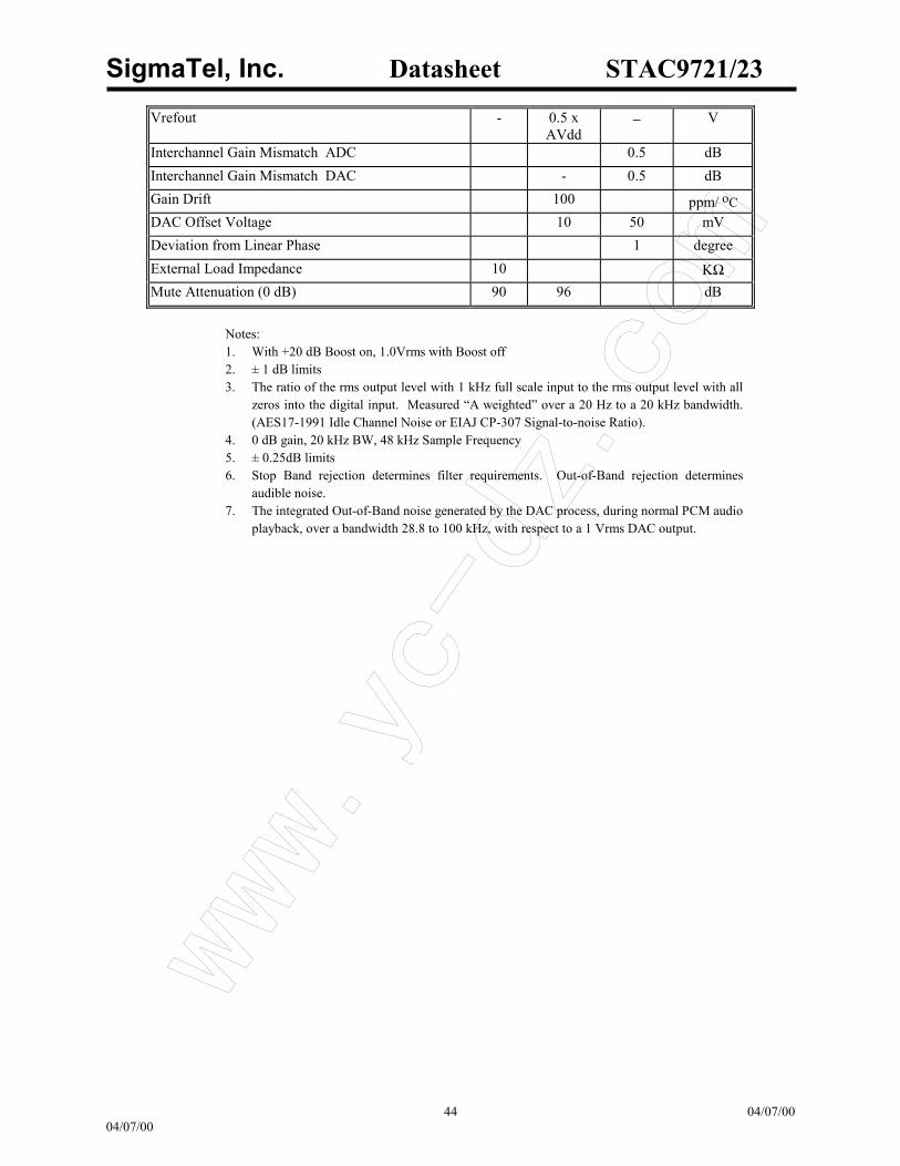
Vrefout - 0.5 x AVdd
− V
Interchannel Gain Mismatch ADC 0.5 dB Interchannel Gain Mismatch DAC - 0.5 dB Gain Drift 100 ppm/ oC DAC Offset Voltage 10 50 mV Deviation from Linear Phase 1 degree External Load Impedance 10 KΩ Mute Attenuation (0 dB) 90 96 dB
Notes: 1. With +20 dB Boost on, 1.0Vrms with Boost off 2. ± 1 dB limits 3. The ratio of the rms output level with 1 kHz full scale input to the rms output level with all
zeros into the digital input. Measured “A weighted” over a 20 Hz to a 20 kHz bandwidth. (AES17-1991 Idle Channel Noise or EIAJ CP-307 Signal-to-noise Ratio).
4. 0 dB gain, 20 kHz BW, 48 kHz Sample Frequency 5. ± 0.25dB limits 6. Stop Band rejection determines filter requirements. Out-of-Band rejection determines
audible noise. 7. The integrated Out-of-Band noise generated by the DAC process, during normal PCM audio
playback, over a bandwidth 28.8 to 100 kHz, with respect to a 1 Vrms DAC output.
www.yc-dz.com
SigmaTel, Inc. Datasheet STAC9721/23
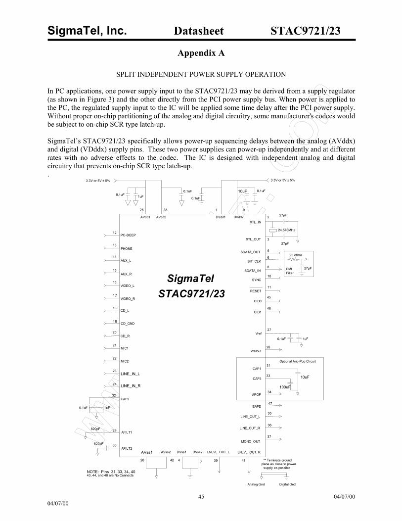
45 04/07/00 04/07/00
Appendix A
SPLIT INDEPENDENT POWER SUPPLY OPERATION In PC applications, one power supply input to the STAC9721/23 may be derived from a supply regulator (as shown in Figure 3) and the other directly from the PCI power supply bus. When power is applied to the PC, the regulated supply input to the IC will be applied some time delay after the PCI power supply. Without proper on-chip partitioning of the analog and digital circuitry, some manufacturer's codecs would be subject to on-chip SCR type latch-up. SigmaTel’s STAC9721/23 specifically allows power-up sequencing delays between the analog (AVddx) and digital (VDddx) supply pins. These two power supplies can power-up independently and at different rates with no adverse effects to the codec. The IC is designed with independent analog and digital circuitry that prevents on-chip SCR type latch-up. .
VIDEO_L
VIDEO_R
AUX_L
AFILT1
AFILT2AVss1 AVss2 DVss1 DVss2
AVdd1 AVdd2 DVdd1 DVdd2
820pF
29
30
14
17
16
744226
3
2
CAP2
XTL_OUT
XTL_IN
24.576MHz
32
1uF
SigmaTelSTAC9721/23
28Vrefout
Vref27
1uF0.1uF
27pF
27pF
LINE_OUT_L
LINE_OUT_R
MONO_OUT
35
36
37
LINE_IN_R24
LINE_IN_L23
PHONE13
PC_BEEP12
MIC222
AUX_R15
MIC121
6
5
8
11
10
SDATA_OUT
SDATA_IN
RESET
SYNC
BIT_CLK
CD_GND
CD_R20
19
18CD_L
Analog Gnd Digital Gnd
NOTE: Pins 31, 33, 34, 4043, 44, and 48 are No Connects
** Teminate groundplane as close to power
supply as possible
LNLVL_OUT_L LNLVL_OUT_R
39 41
46
45
CID1
CID0
820pF
APOP
EAPD
34
47
CAP131
CAP333
0.1uF
Optional Anti-Pop Circuit
100uF
10uF
27pF
22 ohms
EMIFilter
0.1uF 10uF1uF 0.1uF
0.1uF0.1uF
25 38 1 9
3.3V or 5V ± 5%3.3V or 5V ± 5%
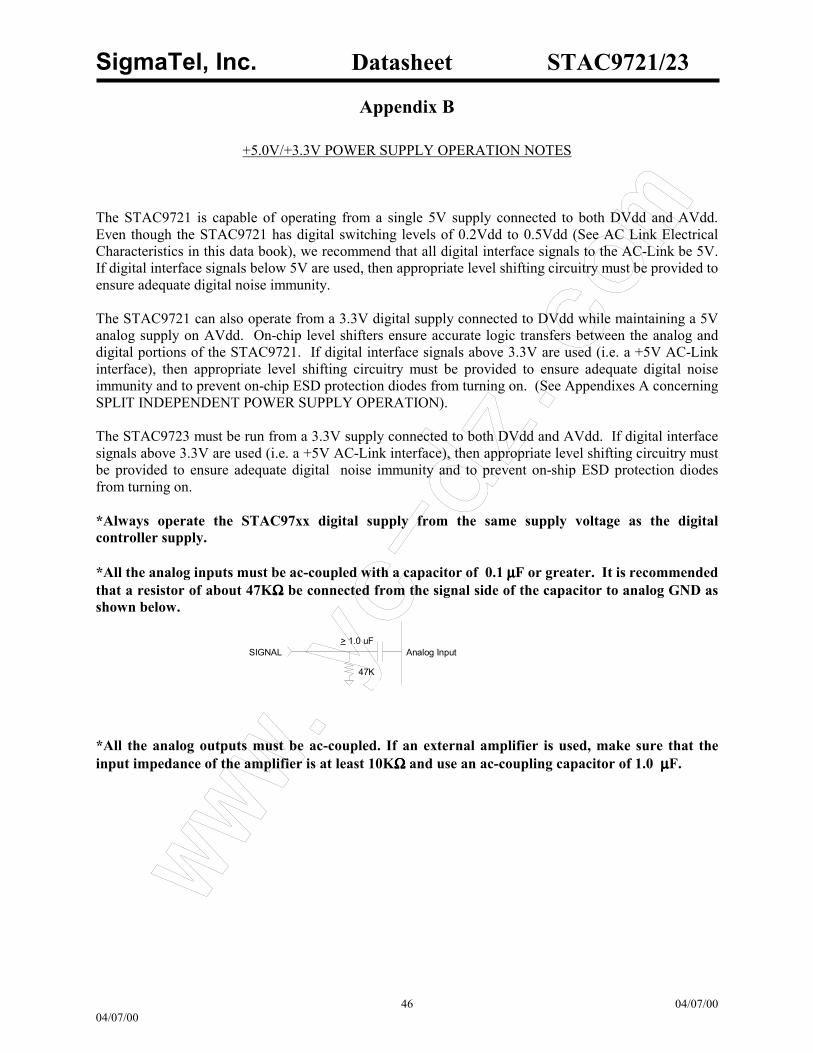
www.yc-dz.com
SigmaTel, Inc. Datasheet STAC9721/23
46 04/07/00 04/07/00
Appendix B
+5.0V/+3.3V POWER SUPPLY OPERATION NOTES The STAC9721 is capable of operating from a single 5V supply connected to both DVdd and AVdd. Even though the STAC9721 has digital switching levels of 0.2Vdd to 0.5Vdd (See AC Link Electrical Characteristics in this data book), we recommend that all digital interface signals to the AC-Link be 5V. If digital interface signals below 5V are used, then appropriate level shifting circuitry must be provided to ensure adequate digital noise immunity. The STAC9721 can also operate from a 3.3V digital supply connected to DVdd while maintaining a 5V analog supply on AVdd. On-chip level shifters ensure accurate logic transfers between the analog and digital portions of the STAC9721. If digital interface signals above 3.3V are used (i.e. a +5V AC-Link interface), then appropriate level shifting circuitry must be provided to ensure adequate digital noise immunity and to prevent on-chip ESD protection diodes from turning on. (See Appendixes A concerning SPLIT INDEPENDENT POWER SUPPLY OPERATION). The STAC9723 must be run from a 3.3V supply connected to both DVdd and AVdd. If digital interface signals above 3.3V are used (i.e. a +5V AC-Link interface), then appropriate level shifting circuitry must be provided to ensure adequate digital noise immunity and to prevent on-ship ESD protection diodes from turning on. *Always operate the STAC97xx digital supply from the same supply voltage as the digital controller supply. *All the analog inputs must be ac-coupled with a capacitor of 0.1 µµµµF or greater. It is recommended that a resistor of about 47KΩΩΩΩ be connected from the signal side of the capacitor to analog GND as shown below.
*All the analog outputs must be ac-coupled. If an external amplifier is used, make sure that the input impedance of the amplifier is at least 10KΩ Ω Ω Ω and use an ac-coupling capacitor of 1.0 µµµµF.
47K
> 1.0 uFSIGNAL Analog Input
www.yc-dz.com
SigmaTel, Inc. Datasheet STAC9721/23
47 04/07/00 04/07/00
- NOTES -
www.yc-dz.com
SigmaTel, Inc. Data Sheet STAC9721
48 04/07/00 04/07/00
For more information, please contact:
SigmaTel, Inc. 6101 W. Courtyard Dr., Bldg. 1, Suite 100
Austin, Texas 78730 Tel (512) 343-6636x29, Fax (512) 343-6199
email: [email protected] http://www.sigmatel.com


![Mixed-Initiative Design of Game Levels: Integrating ... · 2.3 Ludoscope Ludoscope [5, 6, 8] is a mixed-initiative design tool based on the principles of model driven engineering](https://img.pdfslide.us/doc/110x75/5edd5309ad6a402d66685fe0/mixed-initiative-design-of-game-levels-integrating-23-ludoscope-ludoscope.jpg)