Embed Size (px)
Citation preview
Si/Ge Nanowires as High Performance FETs
NE 242 – Electronic Devices
Rajesh Swaminathan#20194189
July 25, 2007
Why semiconducting nanowires?
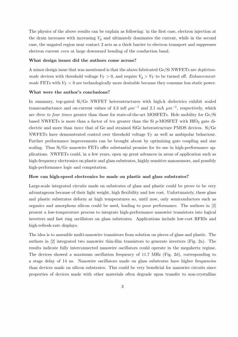
Semiconductor nanowires are potential alternatives to conventional planar (MOSFETs). NanowireFETs (NWFETs) have a unique electronic structure which we can try and exploit. Carriers innanowires have longer mean free paths and are subjected to reduced scattering thanks to one-dimensional quantum confinement effects. Unlike carbon-nanotubes (CNTs), the electronic prop-erties of nanowires are highly reproducible in a large-enough yield required for VLSI systems andapplications. In ref. [1], a nanowire based FET using high-k dielectrics in a top-gate geometry wasreported (Fig. 1a,b,c). This FET displayed enhanced gate coupling, and a scaled transconductance(∂I/∂V ) and “on” current that was three to four times greater than state-of-the-art MOSFETs.Furthermore, the intrinsic switching delay τ substantially exceeded values obtained in planar siliconMOSFETs.
Silicon and germanium nanowires have been studied for a few years but Schottky barriers andscattering from charged dopants have always limited intrinsic mobility and device performance.Lieber et al [1] have demonstrated transparent contacts and low-bias ballistic transport with un-doped Ge/Si core/shell nanowire heterostructures. These heterostructures have a mean free pathas high as 500 nm. Further, enhanced mobility is observed due to reduced scattering and since notone, but several sub-bands may participate in NWFET transport.
What performance benefits were observed?
In reference [1], NWFET high-performance devices using thin HfO2 and ZrO2 high-k gate dielectricswere fabricated (Fig. 1d,e). The family of Id − Vds (Fig. 3a) curves show that the drain current Id
first increases then saturates with increasingly negative drain voltage, similar to a conventional longchannel MOSFET. The authors have demonstrated that the device has a peak transconductance,gm = dId/dVg of 26 µS. The device exhibits a maximum drain current Id(max) of 35 µA at Vg = -2V. The authors note that these values of gm and Id(max) substantially exceed the best performance
1
reported to date in single semiconductor NWFETs. Because the geometric gate capacitance perunit area is only 29% larger than that of conventional Si p-MOSFETs, the large increase in gm andIon cannot be accounted for by an increase in gate capacitance alone. The hole mobility for thisfabricated Ge/Si NWFET is more than ten times better than that of the Si p-MOSFET. The aboveimprovements are attributed to the quasi-1D transport in clean Ge/Si heterostructure nanowires.
Furthermore, no significant short-channel effects were observed for devices down to at least L =190 nm. In general, an FET with a small S is essential for modern logic circuits as it reduces the“off” state current and therefore minimizes static power dissipation.
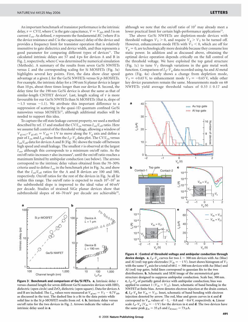
Data obtained for the fabricated NWFET show a clear speed advantage at a given L: the intrinsicdelay τ = CV/I, where C is the gate capacitance and I is the “on” current, for a 190 nm Si planardevice is larger than 10 ps (picoseconds), but this is about three times longer than the intrinsicdelay obtained in the Ge/Si NWFET. This considerable difference is attributed to the suppressionof scattering in the quasi-1D quantum confined Ge/Si nanowires.
The authors have tweaked the design of their NWFET slightly and come up with an asymmetricgate structure (Fig. 5b) to suppress ambipolar conduction which limits the maximum on/off ratiothat can be reached. The new gate design was able to tune the threshold voltage VT through thegate metal work function. Optimal device operation is critically dependent on how well VT canbe controlled, and therefore tunability is easily achievable through a choice of top gate metal withspecific work function in fabrication.
It is well known that Schottky barriers exist at CNT contacts. However, such limitations do notexist for Ge/Si NWFETs which do not have contact barriers, and thus the asymmetrical gatestructure can yield unipolar NWFETs without sacrificing performance.
What challenges were encountered and how were they addressed?
Two major challenges were encountered with the performance of the NWFET. First, a non-idealgate coupling (α < 1) was observed which yielded a larger S value since S ∝ 1/α. This, according tothe authors, was due to a finite trap state density at the nanowire/high-k interface. Optimizing ofthe deposition process of the oxide layer during fabrication should yield improved interface qualityand enable ideal sub-threshold behaviour.
The second challenge encountered was that of ambipolar conduction, i.e. conduction by electroncarriers (as opposed to holes). This type of conduction is detrimental to high-performance appli-cations as it reduces the window of operation and increases the minimum off-state current. Thisissue was addressed with asymmetrical partial gates (Fig. 5b). More importantly, switching thesource and drain electrodes dramatically suppressed the ambipolar current from 300 to 0.8 nA atVds = -1 V.
2
The physics of the above results can be explain as following: in the first case, electron injection atthe drain increases with increasing Vg and ultimately dominates the current, while in the secondcase, the ungated region near contact 2 acts as a thick barrier to electron transport and suppresseselectron current even at large downward bending of the conduction band.
What design issues did the authors come across?
A minor design issue that was mentioned is that the above fabricated Ge/Si NWFETs are depletion-mode devices with threshold voltage VT > 0, and require Vg > VT to be turned off. Enhancement-mode FETs with VT < 0 are technologically more desirable because they consume less static power.
What were the author’s conclusions?
In summary, top-gated Si/Ge NWFET heterostructures with high-k dielectrics exhibit scaledtransconductance and on-current values of 3.3 mS µm−1 and 2.1 mA µm−1, respectively, whichare three to four times greater than those for state-of-the-art MOSFETs. Hole mobility for Ge/Sibased NWFETs is more than a factor of ten greater than the Si p-MOSFET with HfO2 gate di-electric and more than twice that of Ge and strained SiGe heterostructure PMOS devices. Si/GeNWFETs have demonstrated control over threshold voltage VT as well as ambipolar behaviour.Further performance improvements can be brought about by optimizing gate coupling and sizescaling. Thus Si/Ge nanowire FETs offer substantial promise for its use in high-performance ap-plications. NWFETs could, in a few years, open up great advances in areas of application such ashigh-frequency electronics on plastic and glass substrates, highly sensitive nanosensors, and possiblyhigh-performance logic and computation.
How can high-speed electronics be made on plastic and glass substrates?
Large-scale integrated circuits made on substrates of glass and plastic could be prove to be veryadvantageous because of their light weight, high flexibility and low cost. Unfortunately, these glassand plastic substrates deform at high temperatures so, until now, only semiconductors such asorganics and amorphous silicon could be used, leading to poor performance. The authors in [2]present a low-temperature process to integrate high-performance nanowire transistors into logicalinverters and fast ring oscillators on glass substrates. Applications include low-cost RFIDs andhigh-refresh-rate displays.
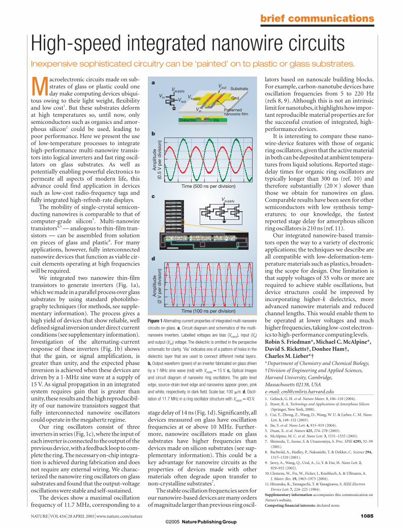
The idea is to assemble multi-nanowire transistors from solution on pieces of glass and plastic. Theauthors in [2] integrated two nanowire thin-film transistors to generate inverters (Fig. 2a). Theresults indicate fully interconnected nanowire oscillators could operate in the megahertz regime.The devices showed a maximum oscillation frequency of 11.7 MHz (Fig. 2d), corresponding toa stage delay of 14 ns. Nanowire oscillators made on glass substrates have higher frequenciesthan devices made on silicon substrates. This could be very beneficial for nanowire circuits sinceproperties of devices made with other materials often degrade upon transfer to non-crystalline
3

substrates.
The techniques described in [2] are all compatible with low-deformation-temperature materials,most importantly plastics. One important limitation is that supply voltages of 35 V or moreare required to achieve stable oscillations. However, the incorporation of high-k dielectrics, moreadvanced nanowire materials and reduced channel lengths could help improve the devices that useglass substrates. Advanced materials integration would enable these devices to be operated at lowervoltages and much higher frequencies.
Can we make high performance logic gates using nanowires?
The authors in [3] suggest a “bottom-up” approach to building electronics from well-defined semi-conductor nanowire building blocks. Crossed nanowire p-n junctions and junction arrays can beassembled to create integrated nanoscale FET arrays which can be configured as OR, AND, andNOR logic-gate structures. These structures exhibit substantial gain and have been used to imple-ment basic computation.
CNTs are unsuited for the task because of our inability to control whether they are semiconductingor metallic. This makes device fabrication an arduous task. Nanowires, on the other hand, can beassembled in a predictable manner because the electronic properties and sizes of the nanowires canbe precisely controlled during fabrication.
The authors in [3] synthesized single-crystal p-Si and n-GaN (gallium nitride) nanowires of diam-eters ranging from 10-30 nm. These nanowires were chosen because the oxide coating on theirsurfaces could be independently varied to enable good control of junction electronic properties.Both nanoscale diodes with low turn-on voltages as well as nanoscale FETs with high turn-onvoltages can be made. In a typical NWFET, where the n-GaN nanowire is used as a nano-gate, wefind a large decrease in conductance with increasing gate voltage. Crossed NWFETs are seen tobe highly sensitive owing to their intrinsically thin gate dielectric between the crossed nanowires.
The bottom-up approach was used to investigate both diode- and FET-based logic gates (Fig. 6).First, a two-input OR gate was created by using a 2(p) by 1(n) cross p-n junction array with thetwo p-Si nanowires as inputs and the n-GaN nanowire as the output. The authors also fabricatedan AND gate from a 1 (p-Si) by 3 (n-GaN) multiple junction array. In this structure, the p-Sinanowire is biased at 5 V; two of the GaN nanowires are used as inputs, and the third is usedas a gate with a constant voltage to create a resistor by depleting a portion of the p-Si nanowire.Finally, a logic NOR gate was assembled by using a 1 (p-Si) by 3 (n-GaN) crossed NW-FET array.The NOR gate was configured with 2.5 V applied to one crossed nanowire FET to create a constantresistance of 100 MΩ, and the p-Si nanowire channel was biased at 5 V.
The two-input NOR gates routinely exhibited gains in excess of five. High gain is a critical char-acteristic of gates because it enables interconnection of arrays of logic gates without signal loss at
4
each stage. The authors also note that a multiple-input NOR gate can function as a NOT gate aswell by eliminating one of the inputs.
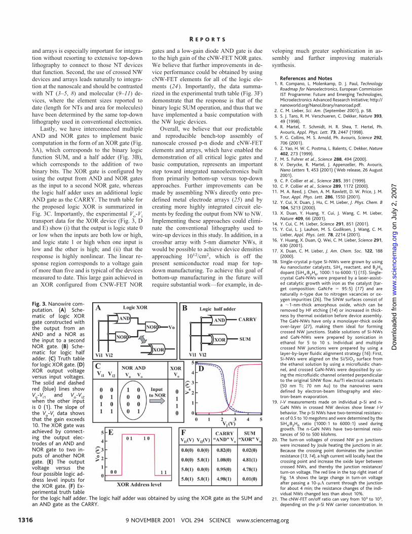
Lastly, the authors interconnected multiple AND and NOR gates to implement basic computationin the form of an XOR gate, which corresponds to the binary logic SUM function. The XOR gateis configured by using the output from AND and NOR gates as the input to a second NOR gate(Fig. 4).
The authors in [3] note that further improvements can be made by assembling nanowires directlyonto predefined metal electrode arrays and by creating more highly integrated circuit elements byfeeding the output from one nanowire to the next.
What is the underlying physics behind nanostructures?
The performance of CMOS is expected to be enhanced by new physical phenomena. This includesquantum effects and ballistic transport in nanoscale devices. Bottom-up-type nanodevices formedby self-assembly are expected to become more prevalent. New types of nanoscale devices such asspin transistors will be integrated. The hope is that new physics that is observed on the nanoscalecan be exploited to enhance the performance of CMOS beyond its scaling limit. Taking advantageof the quantum confinement effect can help us control and improve the performance of CMOS.The carriers within nanoscale narrow- and thin-channel MOSFETs can be confined into a one-dimensional narrow and thin channel respectively. More evidence of quantum effects is observedwhen the channel length is less than 10 nm. Further, the threshold voltage of narrow MOSFETscan be varied and controlled depending on the channel width because the ground energy of carriersis raised by quantum confinement.
Most importantly, the authors of [4] have demonstrated by simulation that the mobility is modifiedin narrow-channel MOSFETs. Larger mobility is observed in [100]-oriented devices: this is dueto the anisotropic effective mass of silicon. Confinement in nanoscale narrow channels is strongerbecause the carriers have only one degree of freedom. The stronger the confinement, the greater themobility. We also find that the thinner the silicon substrate, the lower the mobility due to increasedacoustic phonon scattering. But p-MOSFETs have good mobility even with small thickness becausethe predominant scattering mechanism is scattering induced by silicon-on-insulator (SOI) thicknessfluctuation. However, p-MOSFETs are less sensitive to SOI-thickness-fluctuation-induced scatter-ing due to heavier hole effective mass normal to the channel surface. Thus in nanoscale CMOS,the crystal orientation, channel direction, and device dimension should be carefully determined inorder to maximize device performance.
5
How can we exploit nanostructure physics for applications?
Note to TA: The following section is not an expected deliverable but exists solely for completeness.It is therefore not expected to count towards the 5-page limit.
The authors in [4] have a demonstrated a new function in silicon nanocrystal memories: sili-con nanocrystals embedded in gate oxide act as site for charge storages. Physical separation ofnanocrystals can improve the retention time by limiting lateral flow of charges.
A single-electron transistor is one of the best known nanoscale devices. A single-electron transistor,in the form of a point-contact MOSFET is made from a silicon quantum dot that is self-formed inthe very narrow channel. Unfortunately, single-electron transistors generally operate only at verylow temperatures. The operation temperature may be raised by making the quantum dot smaller.Currently, the dot size is 2 nm. Since the dot is extremely small, the quantum-level spacing inthe dot is not negligible, and negative differential conductance (NDC) due to resonant tunneling isobserved at room temperature. At room temperature, two integrated single-hole transistors exhibitCoulomb blockade oscillations and form a directional current switch. Moreover, each single-holetransistor has silicon nanocrystals embedded in the gate oxide which act as nonvolatile memory.
Further applications of single-electron/hole transistors are in digital circuit applications in the formof an XOR circuit, and an analog circuit application in the form of an analog pattern matchingcircuit since the Coulomb blockade oscillations have bell-shaped I-V characteristics.
6

References
[1] Ge/Si nanowire heterostructures as high-performance field-effect transistors.
Jie Xiang, Wei Lu, Yongjie Hu, Yue Wu, Hao Yan, and Charles M. Lieber. Nature, 25 May2006; 441: 489-493.
[2] High-speed integrated nanowire circuits.
R.S. Friedman, M.C. McAlpine, D.S. Ricketts, D. Ham and C.M. Lieber. Nature, 28 April2005; 434: 1085.
[3] Logic gates and computation from assembled nanowire building blocks.
Yu Huang, Xiangfeng Duan, Yi Cui, Lincoln J. Lauhon, Kyoung-Ha Kim, and Charles M.Lieber. Science, 9 November 2001; 294 (5545): 1313.
[4] Emerging nanoscale silicon devices taking advantage of nanostructure physics. T.Hiramoto, M. Saitoh, G. Tsutsui. IBM journal of R&D, July/September 2006; Volume 50,Number 4/5.
© 2006 Nature Publishing Group
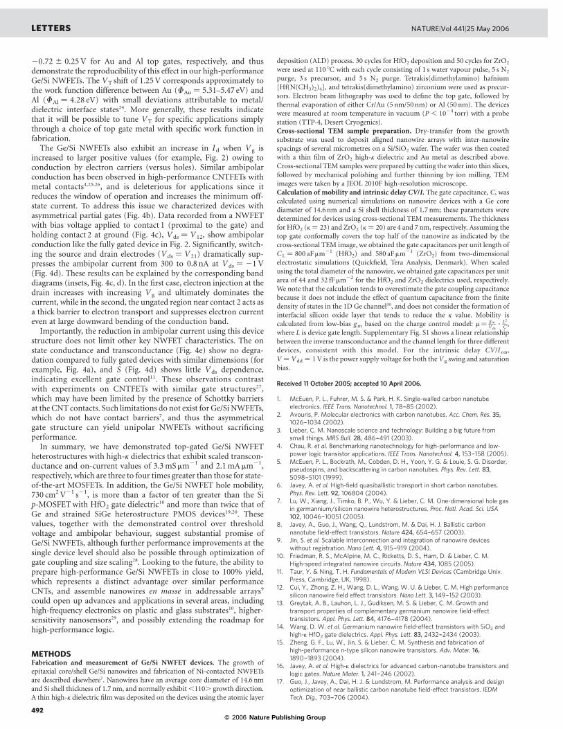
Ge/Si nanowire heterostructures as high-performance field-effect transistorsJie Xiang1*, Wei Lu1*, Yongjie Hu1, Yue Wu1, Hao Yan1 & Charles M. Lieber1,2
Semiconducting carbon nanotubes1,2 and nanowires3 are potentialalternatives to planar metal-oxide-semiconductor field-effecttransistors (MOSFETs)4 owing, for example, to their uniqueelectronic structure and reduced carrier scattering caused byone-dimensional quantum confinement effects1,5. Studies havedemonstrated long carrier mean free paths at room temperaturein both carbon nanotubes1,6 and Ge/Si core/shell nanowires7. Inthe case of carbon nanotube FETs, devices have been fabricatedthat work close to the ballistic limit8. Applications of high-performance carbon nanotube FETs have been hindered, however,by difficulties in producing uniform semiconducting nanotubes, afactor not limiting nanowires, which have been prepared withreproducible electronic properties in high yield as required forlarge-scale integrated systems3,9,10. Yet whether nanowire field-effect transistors (NWFETs) can indeed outperform their planarcounterparts is still unclear4. Here we report studies onGe/Si core/shell nanowire heterostructures configured as FETs using high-kdielectrics in a top-gate geometry. The clean one-dimensionalhole-gas in the Ge/Si nanowire heterostructures7 and enhancedgate coupling with high-k dielectrics give high-performance FETsvalues of the scaled transconductance (3.3mS mm21) and on-current (2.1mA mm21) that are three to four times greater thanstate-of-the-art MOSFETs and are the highest obtained onNWFETs. Furthermore, comparison of the intrinsic switchingdelay, t 5 CV/I, which represents a key metric for device appli-cations4,11, shows that the performance of Ge/Si NWFETs iscomparable to similar length carbon nanotube FETs and substan-tially exceeds the length-dependent scaling of planar siliconMOSFETs.Silicon9,10,12 and germanium13,14 nanowires have been the focus of
recent studies of one-dimensional (1D) FETs. However, metal con-tacts to single-component nanowires generally produce Schottkybarriers that limit device performance15, and moreover, scatteringfrom charged dopants can also reduce the intrinsic mobility of thesenanowire devices15. In contrast, we have recently demonstratedtransparent contacts and low-bias ballistic transport7 in undoped Ge/Si core/shell nanowire heterostructures (Fig. 1a, b), with an estimatedscatteringmean free path of,500 nm. The 1D sub-band spacing in thetypical 15-nm core Ge/Si nanowires determined through both experi-mental measurements and theoretical calculations7 is ,25meV, andthus at room temperature several sub-bands may participate inNWFET transport. While the Ge/Si nanowire devices will not bestrictly 1D, the limited number of conduction channels and cleanmaterial structure can benefit performance through, for example, areduction in scattering. To explore the potential of Ge/Si nanowireheterostructures as high-performance FETs we have fabricated (seeMethods) devices using thinHfO2 or ZrO2 high-k gate dielectrics andmetal top gate electrodes (Fig. 1c, d). Cross-sectional transmissionelectron microscopy (TEM) images (Fig. 1e) show that both the
high-k and metal top gate conform to the approximately circularcross-section of the nanowire, and also verify the Ge/Si core/shellstructure. The conformal top gate structure approaches an idealcylindrical gate geometry, and together with the high-k dielectricsproduces a much more efficient gate response than previous studiesusing lower-k SiO2 dielectric and planar back gates9,12,16.Typical output and transfer characteristics recorded from a Ge/Si
device fabricated in this way with a channel length, L ¼ 1 mm and atotal diameter of 18 nm (device A) are shown in Fig. 2a, b. The familyof Id–Vds curves (Fig. 2a) show that the drain current Id firstincreases then saturates with increasingly negative drain voltage,similar to a conventional long channel MOSFET11. These data alsoshow that Id increases as the gate voltageVg decreases from 1 to22V,and thus that the device is a p-type depletion-mode FET. This p-typeFET behaviour is expected from the band diagram in Fig. 1b, wherethe Fermi level lies below the Ge valence band edge in the absence of agate. The Id–Vg transfer curve recorded for the drain bias voltage
LETTERS
Figure 1 | Ge/Si core/shell NWFET. a, Schematic of a Ge/Si core/shellnanowire. b, Cross-sectional diagram showing the formation of hole-gas inthe Ge quantum well confined by the epitaxial Si shell, where CB is theconduction band and VB is the valence band. The dashed line indicates theFermi level, EF. The valence band offset of ,500meV between Ge and Siserves as a confinement potential to the hole-gas as discussed previously7.c, Schematic of the NWFET device with high-k dielectric layer and Au topgate. d, Top-view SEM image of a typical device. The Au top gate overlapswith the Ni source/drain electrodes to ensure full coverage of the channel.Scale bar, 500 nm. e, Cross-sectional TEM image of a device prepared using7 nm ZrO2 dielectric. Dotted lines are guides to the eye showing boundariesbetween different materials denoted in the image. The nanowire is tilted offthe imaging axis. Scale bar, 10 nm.
1Department of Chemistry and Chemical Biology, 2Division of Engineering and Applied Sciences, Harvard University, Cambridge, Massachusetts 02138, USA.*These authors contributed equally to this work.
Vol 441|25 May 2006|doi:10.1038/nature04796
489

© 2006 Nature Publishing Group
Vds ¼ 21V (Fig. 2b) demonstrates that the NWFET has a peaktransconductance, gm ¼ dId/dVg, of 26 mS. In addition, the deviceexhibits a maximum drain current Id(max) of 35 mA at Vg ¼ 22V.We note these values of gm and Id(max) substantially exceed the
best performance reported to date in single semiconductorNWFETs12,14.The on current Ion for a FET device is usually determined at
Vg ¼ Vds ¼ Vdd, where Vdd is the power supply voltage and equals1 V in our case. Following conventions in planar devices, we define onand off currents as the valuesmeasured atVg(on) ¼ VT 2 0.7Vdd andVg(off) ¼ VT þ 0.3Vdd, so that 30% of the Vg swing above thethreshold voltage VT is applied to turn the device off, while theremaining 70% sets the operation range of the on state (Fig. 2b).Similar methods have been proposed in benchmarking carbonnanotube FET devices4,17. From Fig. 2b, we obtain Ion ¼ 14mA forthis 1-mm-long device. Significantly, the scaled values of gm and Ion,1.4mS mm21 and 0.78mA mm21, using the total nanowire diameteras the device width, already exceeds the values of 0.8mS mm21 and0.71mA mm21 recently reported in much shorter, sub-100-nmsilicon p-MOSFETs employing high-k dielectrics18.In addition, we have prepared and studied a large number of Ge/Si
NWFET devices with L varying from 1 mm to 190 nm; essentially allof these devices exhibited high-performance behaviour and testify tothe reproducibility of both the Ge/Si nanowires and contacts to thismaterial. Representative data obtained from a L ¼ 190 nm device(device B), which should exhibit larger gm and Id values owing toreduced channel resistance, are shown in Fig. 2c. These data yieldgm ¼ 60 mS, Ion ¼ 37 mA (Vdd ¼ 1 V), and Id(max) ¼ 91 mA, andcorrespond to scaled values of gm and Ion of 3.3mS mm21 and2.1mA mm21, respectively. Notably, these values are more thantwice that achieved in the longer channel device and are 3–4 timesgreater than state-of-the-art Si p-MOSFETs18. The geometric gatecapacitance per unit area in our NWFETs, 44 fFmm22 (Methods),is only 29% larger than the 34 fFmm22 in these Si p-MOSFETs18.Therefore the large gain in gm and Ion cannot be accounted for by anincrease in gate capacitance alone. Moreover, the hole mobility forthis Ge/Si NWFET, 730 cm2V21 s21, extracted at the linear region(jVdsj ¼ 10mV) from the peak gm ¼ 3 mS at jVg 2 VTj ¼ 0.13Vusing the charge control model, represents an improvement of morethan a factor of ten over that of the Si p-MOSFET with HfO2 gatedielectric (50–60 cm2V21 s21)18, and also is more than twice thereported low-field mobility of Ge and strained SiGe heterostructurePMOS devices19,20. Improved mobility is observed for NWFETs withchannel lengths from 0.19 to 1mm (Supplementary Fig. S1), with anaverage of 640 cm2V21 s21. These improvements over planar devicestructures thus verify the performance benefit due to the quasi-1Dtransport in clean Ge/Si heterostructure nanowires.The subthreshold region of the Id–Vg data was also analysed and
yields values of the slope, S ¼ 2[d(log10Id)/dVg]21, of 105 and
100mV per decade for the L ¼ 1 mm and 190 nm NWFETs, respect-ively, for Vds ¼ 21V (Fig. 2b, c). Similar values of S were obtainedfrom Id–Vg data recorded on both devices using Vds from 20.01 to21 V, which indicate the absence of significant short-channeleffects11 for devices down to at least L ¼ 190 nm and excellent Vg
control of the channel potential over the competing effect of drain-induced barrier lowering at larger biases11.In general, an FET with a small S is essential for modern logic
circuits as it reduces the off state current and minimizes static powerdissipation. The value of S can be estimated11 by 2.3kBT/ea, where Tis temperature and a is the gate-coupling factor, which yields a roomtemperature minimum (a ¼ 1) of 60mV per decade. The values of Sdetermined for the L ¼ 1 mm and 190 nm Ge/Si NWFETs aresuperior to the best value (140mV per decade) reported previously9
for NWFETs but still larger than the theoretical minimum. The non-ideal gate coupling (a , 1), which yields this larger S value, isprobably due to a finite trap state density at the nanowire/high-kinterface21. Optimization of the high-k deposition process duringfabrication or growth of a cylindrical high-k shell on the Ge/Sinanowire before fabrication should yield improved interface qualityand enable us to approach ideal subthreshold behaviour in the futurein these NWFETs.
Figure 2 | Characteristics of high-performance Ge/Si NWFET. a, Id–Vds
data for device A (L ¼ 1 mm, 4 nm HfO2 dielectric) with Vg ¼ 22 to 2V in0.25V steps from top to bottom. b, Id–Vg for device A with blue, red, andgreen data points corresponding to Vds values of 21, 20.5 and 20.01V,respectively. The leakage current through the gate electrode (Ig) is,10210 A, which excludes Ig as source of increase in Id at Vg . ,0.5 V.Inset, linear scale plot of Id versus Vg measured at Vds ¼ 21V. The blue-shaded area defines the 1V gate voltage window described in the text, whereVT was determined from the intercept of the tangent of maximum slope(linear transconductance) region of the Id–Vg curve
11. c, Id–Vg data fordevice B (L ¼ 190 nm, 4 nm HfO2 dielectric) with blue, red and green datapoints corresponding to Vds values of 21, 20.1 and 20.01V, respectively.Inset, linear scale plot of Id versus Vg measured at Vds ¼ 21V.
LETTERS NATURE|Vol 441|25 May 2006
490
© 2006 Nature Publishing Group
An important benchmark of transistor performance is the intrinsicdelay, t ¼ CV/I, whereC is the gate capacitance,V ¼ Vdd, and I is oncurrent Ion. As defined, t represents the fundamental RC (where R isthe device resistance and C is the capacitance) delay of the device andprovides a frequency limit for transistor operation that is relativelyinsensitive to gate dielectrics and device width, and thus represents agood parameter for comparing different types of devices11. Thecalculated intrinsic delays are 57 and 4 ps for devices A and B inFig. 2, respectively, whereCwas determined by numerical simulation(Methods). A summary of the results from seven Ge/Si NWFETsversus L and the corresponding scaling for Si MOSFETs (Fig. 3a)highlights several key points. First, the data show clear speedadvantage at a given L for the Ge/Si NWFETs versus Si p-MOSFETs.For example, the intrinsic delay for a 190 nm Si planar device is largerthan 10 ps, about three times longer than our device B. Second, thedelay time for the 190 nm Ge/Si device is about the same as that ofsimilar-length CNTFET devices4. Last, length scaling of t is morefavourable for our Ge/Si NWFETs than Si MOSFETs (that is, slope of,1.5 versus ,1.1). We attribute this important difference to asuppression of scattering in the quasi-1D quantum confined Ge/Sinanowires versus MOSFETs22, although additional studies will beneeded to support this idea.To capture the off state leakage current property, we used amethod
described by ref. 17 and studied the CV/Ion versus Ion/Ioff ratio. Herewe assume full control of the threshold voltage, allowing a window ofVg(on)–Vg(off) ¼ Vdd ¼ 1V to move along the Vg axis and define apair of Ion and Ioff value from the Id–Vg data plot. The CV/Ion versusIon/Ioff data for devices A and B (Fig. 3b) shows the trade-off betweenhigh speed and small leakage. The smallest t is observed at the largestIon, although this corresponds to a minimum on/off ratio. As theon/off ratio increases t also increases4, until the on/off ratio reaches amaximum limited by ambipolar conduction (see below). The arrowscorrespond to the intrinsic delay values obtained from the 70–30%criteria used to define Ion in the benchmark plot in Fig. 3a, and showthat the Ion/Ioff ratios for the A and B devices are 100 and 580,respectively. On/off ratios for the rest of the devices in Fig. 3a all liewithin this range. The on/off ratio is expected to reach 104–105 asthe subthreshold slope is improved to the ideal value of 60mVper decade. Studies of strained SiGe planar devices show thatsubthreshold slopes of 66–70mV per decade are achievable20,
although we note that the on/off ratio of 102 may already meet alower practical limit for certain high-performance applications23.The above Ge/Si NWFETs are depletion-mode devices with
threshold voltages VT . 0, and require Vg . VT to be turned off.However, enhancement-mode FETs with VT , 0, which are off forVg ¼ 0, are technologically more desirable because they consume lessstatic power. In addition and as discussed above, obtaining theoptimal device operation depends critically on the full control ofthe threshold voltage. We have exploited the top gated structure(Fig. 1c) to tune VT through variations in the gate metal workfunction. Comparison of Id–Vg data recorded using Au and Al metalgates (Fig. 4a) clearly shows a change from depletion mode,VT ¼ þ0.65 V, to enhancement mode VT ¼ 20.65V, while otherkey device parameters remain the same. Measurements made on 68NWFETs yield average threshold values of 0.53 ^ 0.17 and
Figure 3 | Benchmark and comparison of Ge/Si FETs. a, Intrinsic delay tversus channel length for seven different Ge/Si nanowire devices with HfO2
dielectric (open circle) and ZrO2 dielectric (open square). Data for devices Aand B are included. The Ion values were measured at Vg(on) ¼ VT 2 0.7Vdd,as discussed in the text. The dashed line is a fit to the data points whilesolid line is the Si p-MOSFET results from ref. 4. b, Intrinsic delay versuson/off ratio for the two devices in Fig. 2. Arrows indicate the values ofintrinsic delay used in a.
Figure 4 | Control of threshold voltage and ambipolar conduction throughdevice design. a, Id–Vg curves for two L ¼ 300 nm devices with Au (blue)and Al (red) top gate electrodes (Vds ¼ 21V). Inset shows histogram of VT
with the sameV g axis for a total of 68 L ¼ 300 nmdevices with Au (blue) andAl (red) top gates. Solid lines correspond to gaussian fits to the twodistributions. b, Schematic and SEM image of the asymmetrical gatestructure designed to suppress ambipolar conduction. Scale bar, 300 nm.c, Id–Vg of partially gated device with ambipolar conduction; bias wasapplied to contact 1 (Vds ¼ V12). Inset, schematic of band bending in theNWFETat finite bias. Arrow denotes electron injection at the drain contact.d, Id–Vg for Vds ¼ V21. Inset, schematic of band bending with electroninjection denoted by arrow. The red, blue and green curves in c and dcorrespond to Vds values of 21, 20.8 and 20.6 V, respectively. e, Linearscale Id–Vg (Vds ¼ 21V) for the devices in c and d. The two devices havethe same peak gm ¼ 35 mS and Id(max) ¼ 73 mA.
NATURE|Vol 441|25 May 2006 LETTERS
491
© 2006 Nature Publishing Group
20.72 ^ 0.25 V for Au and Al top gates, respectively, and thusdemonstrate the reproducibility of this effect in our high-performanceGe/Si NWFETs. The VT shift of 1.25V corresponds approximately tothe work function difference between Au (FAu ¼ 5.31–5.47 eV) andAl (FAl ¼ 4.28 eV) with small deviations attributable to metal/dielectric interface states24. More generally, these results indicatethat it will be possible to tune VT for specific applications simplythrough a choice of top gate metal with specific work function infabrication.The Ge/Si NWFETs also exhibit an increase in Id when Vg is
increased to larger positive values (for example, Fig. 2) owing toconduction by electron carriers (versus holes). Similar ambipolarconduction has been observed in high-performance CNTFETs withmetal contacts4,25,26, and is deleterious for applications since itreduces the window of operation and increases the minimum off-state current. To address this issue we characterized devices withasymmetrical partial gates (Fig. 4b). Data recorded from a NWFETwith bias voltage applied to contact 1 (proximal to the gate) andholding contact 2 at ground (Fig. 4c), Vds ¼ V12, show ambipolarconduction like the fully gated device in Fig. 2. Significantly, switch-ing the source and drain electrodes (Vds ¼ V21) dramatically sup-presses the ambipolar current from 300 to 0.8 nA at Vds ¼ 21V(Fig. 4d). These results can be explained by the corresponding banddiagrams (insets, Fig. 4c, d). In the first case, electron injection at thedrain increases with increasing Vg and ultimately dominates thecurrent, while in the second, the ungated region near contact 2 acts asa thick barrier to electron transport and suppresses electron currenteven at large downward bending of the conduction band.Importantly, the reduction in ambipolar current using this device
structure does not limit other key NWFET characteristics. The onstate conductance and transconductance (Fig. 4e) show no degra-dation compared to fully gated devices with similar dimensions (forexample, Fig. 4a), and S (Fig. 4d) shows little Vds dependence,indicating excellent gate control11. These observations contrastwith experiments on CNTFETs with similar gate structures27,which may have been limited by the presence of Schottky barriersat the CNT contacts. Such limitations do not exist for Ge/Si NWFETs,which do not have contact barriers7, and thus the asymmetricalgate structure can yield unipolar NWFETs without sacrificingperformance.In summary, we have demonstrated top-gated Ge/Si NWFET
heterostructures with high-k dielectrics that exhibit scaled transcon-ductance and on-current values of 3.3mS mm21 and 2.1mA mm21,respectively, which are three to four times greater than those for state-of-the-art MOSFETs. In addition, the Ge/Si NWFET hole mobility,730 cm2V21 s21, is more than a factor of ten greater than the Sip-MOSFET with HfO2 gate dielectric
18 and more than twice that ofGe and strained SiGe heterostructure PMOS devices19,20. Thesevalues, together with the demonstrated control over thresholdvoltage and ambipolar behaviour, suggest substantial promise ofGe/Si NWFETs, although further performance improvements at thesingle device level should also be possible through optimization ofgate coupling and size scaling28. Looking to the future, the ability toprepare high-performance Ge/Si NWFETs in close to 100% yield,which represents a distinct advantage over similar performanceCNTs, and assemble nanowires en masse in addressable arrays9
could open up advances and applications in several areas, includinghigh-frequency electronics on plastic and glass substrates10, higher-sensitivity nanosensors29, and possibly extending the roadmap forhigh-performance logic.
METHODSFabrication and measurement of Ge/Si NWFET devices. The growth ofepitaxial core/shell Ge/Si nanowires and fabrication of Ni-contacted NWFETsare described elsewhere7. Nanowires have an average core diameter of 14.6 nmand Si shell thickness of 1.7 nm, and normally exhibit,110. growth direction.A thin high-k dielectric film was deposited on the devices using the atomic layer
deposition (ALD) process. 30 cycles for HfO2 deposition and 50 cycles for ZrO2
were used at 110 8C with each cycle consisting of 1 s water vapour pulse, 5 s N2
purge, 3 s precursor, and 5 s N2 purge. Tetrakis(dimethylamino) hafnium[Hf(N(CH3)2)4], and tetrakis(dimethylamino) zirconium were used as precur-sors. Electron beam lithography was used to define the top gate, followed bythermal evaporation of either Cr/Au (5 nm/50 nm) or Al (50 nm). The deviceswere measured at room temperature in vacuum (P , 1024 torr) with a probestation (TTP-4, Desert Cryogenics).Cross-sectional TEM sample preparation. Dry-transfer from the growthsubstrate was used to deposit aligned nanowire arrays with inter-nanowirespacings of several micrometres on a Si/SiO2 wafer. The wafer was then coatedwith a thin film of ZrO2 high-k dielectric and Au metal as described above.Cross-sectional TEM samples were prepared by cutting the wafer into thin slices,followed by mechanical polishing and further thinning by ion milling. TEMimages were taken by a JEOL 2010F high-resolution microscope.Calculation of mobility and intrinsic delay CV/I. The gate capacitance, C, wascalculated using numerical simulations on nanowire devices with a Ge corediameter of 14.6 nm and a Si shell thickness of 1.7 nm; these parameters weredetermined for devices using cross-sectional TEMmeasurements. The thicknessfor HfO2 (k ¼ 23) and ZrO2 (k ¼ 20) are 4 and 7 nm, respectively. Assuming thetop gate conformally covers the top half of the nanowire as indicated by thecross-sectional TEM image, we obtained the gate capacitances per unit length ofCL ¼ 800 aF mm21 (HfO2) and 580 aF mm21 (ZrO2) from two-dimensionalelectrostatic simulations (Quickfield, Tera Analysis, Denmark). When scaledusing the total diameter of the nanowire, we obtained gate capacitances per unitarea of 44 and 32 fF mm22 for the HfO2 and ZrO2 dielectrics used, respectively.We note that the calculation tends to overestimate the gate coupling capacitancebecause it does not include the effect of quantum capacitance from the finitedensity of states in the 1D Ge channel30, and does not consider the formation ofinterfacial silicon oxide layer that tends to reduce the k value. Mobility iscalculated from low-bias gm based on the charge control model: m¼
gmVds
L2
C ,where L is device gate length. Supplementary Fig. S1 shows a linear relationshipbetween the inverse transconductance and the channel length for three differentdevices, consistent with this model. For the intrinsic delay CV/I on,V ¼ Vdd ¼ 1V is the power supply voltage for both the Vg swing and saturationbias.
Received 11 October 2005; accepted 10 April 2006.
1. McEuen, P. L., Fuhrer, M. S. & Park, H. K. Single-walled carbon nanotubeelectronics. IEEE Trans. Nanotechnol. 1, 78–-85 (2002).
2. Avouris, P. Molecular electronics with carbon nanotubes. Acc. Chem. Res. 35,1026–-1034 (2002).
3. Lieber, C. M. Nanoscale science and technology: Building a big future fromsmall things. MRS Bull. 28, 486–-491 (2003).
4. Chau, R. et al. Benchmarking nanotechnology for high-performance and low-power logic transistor applications. IEEE Trans. Nanotechnol. 4, 153–-158 (2005).
5. McEuen, P. L., Bockrath, M., Cobden, D. H., Yoon, Y. G. & Louie, S. G. Disorder,pseudospins, and backscattering in carbon nanotubes. Phys. Rev. Lett. 83,5098–-5101 (1999).
6. Javey, A. et al. High-field quasiballistic transport in short carbon nanotubes.Phys. Rev. Lett. 92, 106804 (2004).
7. Lu, W., Xiang, J., Timko, B. P., Wu, Y. & Lieber, C. M. One-dimensional hole gasin germannium/silicon nanowire heterostructures. Proc. Natl. Acad. Sci. USA102, 10046–-10051 (2005).
8. Javey, A., Guo, J., Wang, Q., Lundstrom, M. & Dai, H. J. Ballistic carbonnanotube field-effect transistors. Nature 424, 654–-657 (2003).
9. Jin, S. et al. Scalable interconnection and integration of nanowire deviceswithout registration. Nano Lett. 4, 915–-919 (2004).
10. Friedman, R. S., McAlpine, M. C., Ricketts, D. S., Ham, D. & Lieber, C. M.High-speed integrated nanowire circuits. Nature 434, 1085 (2005).
11. Taur, Y. & Ning, T. H. Fundamentals of Modern VLSI Devices (Cambridge Univ.Press, Cambridge, UK, 1998).
12. Cui, Y., Zhong, Z. H., Wang, D. L., Wang, W. U. & Lieber, C. M. High performancesilicon nanowire field effect transistors. Nano Lett. 3, 149–-152 (2003).
13. Greytak, A. B., Lauhon, L. J., Gudiksen, M. S. & Lieber, C. M. Growth andtransport properties of complementary germanium nanowire field-effecttransistors. Appl. Phys. Lett. 84, 4176–-4178 (2004).
14. Wang, D. W. et al. Germanium nanowire field-effect transistors with SiO2 andhigh-k HfO2 gate dielectrics. Appl. Phys. Lett. 83, 2432–-2434 (2003).
15. Zheng, G. F., Lu, W., Jin, S. & Lieber, C. M. Synthesis and fabrication ofhigh-performance n-type silicon nanowire transistors. Adv. Mater. 16,1890–-1893 (2004).
16. Javey, A. et al. High-k dielectrics for advanced carbon-nanotube transistors andlogic gates. Nature Mater. 1, 241–-246 (2002).
17. Guo, J., Javey, A., Dai, H. J. & Lundstrom, M. Performance analysis and designoptimization of near ballistic carbon nanotube field-effect transistors. IEDMTech. Dig., 703–-706 (2004).
LETTERS NATURE|Vol 441|25 May 2006
492
© 2006 Nature Publishing Group
18. Chau, R. et al. High-k/metal-gate stack and its MOSFET characteristics. IEEEElec. Dev. Lett. 25, 408–-410 (2004).
19. Ritenour, A. et al. Epitaxial strained germanium p-MOSFETs with HfO2 gatedielectric and TaN gate electrode. IEDM Tech. Dig., 433–-436 (2003).
20. Aberg, I., Nı Chleirigh, C., Olubuyide, O. O., Duan, X. & Hoyt, J. L. High electronand hole mobility enhancements in thin-body strained Si/strained SiGe/strained Si heterostructures on insulator. IEDM Tech. Dig., 173–-176 (2004).
21. Wallace, R. M. & Wilk, G. High-k gate dielectric materials. MRS Bull. 27,192–-197 (2002).
22. Wang, J., Polizzi, E., Ghosh, A., Datta, S. & Lundstrom, M. A theoreticalinvestigation of surface roughness scattering in silicon nanowire transistors.Appl. Phys. Lett. 87, 043101 (2005).
23. Wang, J. & Lundstrom, M. Does source-to-drain tunneling limit the ultimatescaling of MOSFETs? IEDM Tech. Dig., 707–-710 (2002).
24. Yeo, Y. C., King, T. J. & Hu, C. M. Metal-dielectric band alignment and itsimplications for metal gate complementary metal-oxide-semiconductortechnology. J. Appl. Phys. 92, 7266–-7271 (2002).
25. Martel, R. et al. Ambipolar electrical transport in semiconducting single-wallcarbon nanotubes. Phys. Rev. Lett. 87, 256805 (2001).
26. Javey, A. et al. Carbon nanotube field-effect transistors with integrated ohmiccontacts and high-k gate dielectrics. Nano Lett. 4, 447–-450 (2004).
27. Lin, Y. M., Appenzeller, J. & Avouris, P. Ambipolar-to-unipolar conversion ofcarbon nanotube transistors by gate structure engineering. Nano Lett. 4,947–-950 (2004).
28. Guo, J., Wang, J., Polizzi, E., Datta, S. & Lundstrom, M. Electrostatics ofnanowire transistors. IEEE Trans. Nanotechnol. 2, 329–-334 (2003).
29. Patolsky, F. & Lieber, C. M. Nanowire nanosensors. Mater. Today 8, 20–-28(2005).
30. Guo, J., Lundstrom, M. & Datta, S. Performance projections for ballisticcarbon nanotube field-effect transistors. Appl. Phys. Lett. 80, 3192–-3194(2002).
Supplementary Information is linked to the online version of the paper atwww.nature.com/nature.
Acknowledgements We thank C. Y. Wen for help with cross-sectional TEMstudy and M. Radosavljevic for discussions. C.M.L. acknowledges support of thiswork by the Defense Advanced Projects Research Agency and Intel.
Author Contributions J.X., W.L., Y.H., Y.W. and H.Y. performed theexperiments. J.X. and W.L. performed data analyses. J.X., W.L. and C.M.L.designed the experiments, discussed the interpretation of results and co-wrotethe paper.
Author Information Reprints and permissions information is available atnpg.nature.com/reprintsandpermissions. The authors declare no competingfinancial interests. Correspondence and requests for materials should beaddressed to C.M.L. ([email protected]).
NATURE|Vol 441|25 May 2006 LETTERS
493
Macroelectronic circuits made on sub-strates of glass or plastic could oneday make computing devices ubiqui-
tous owing to their light weight, flexibilityand low cost1. But these substrates deformat high temperatures so, until now, onlysemiconductors such as organics and amor-phous silicon2 could be used, leading topoor performance. Here we present the useof low-temperature processes to integratehigh-performance multi-nanowire transis-tors into logical inverters and fast ring oscil-lators on glass substrates. As well aspotentially enabling powerful electronics topermeate all aspects of modern life, thisadvance could find application in devicessuch as low-cost radio-frequency tags andfully integrated high-refresh-rate displays.
The mobility of single-crystal semicon-ducting nanowires is comparable to that ofcomputer-grade silicon3. Multi-nanowiretransistors4,5 — analogous to thin-film tran-sistors — can be assembled from solution on pieces of glass and plastic6. For manyapplications, however, fully interconnectednanowire devices that function as viable cir-cuit elements operating at high frequencieswill be required.
We integrated two nanowire thin-filmtransistors to generate inverters (Fig. 1a),which we made in a parallel process over glasssubstrates by using standard photolitho-graphy techniques (for methods, see supple-mentary information). The process gives ahigh yield of devices that show reliable, welldefined signal inversion under direct currentconditions (see supplementary information).Investigation of the alternating-currentresponse of these inverters (Fig. 1b) showsthat the gain, or signal amplification, isgreater than unity, and the expected phaseinversion is achieved when these devices aredriven by a 1-MHz sine wave at a supply of15 V. As signal propagation in an integratedsystem requires gain that is greater thanunity,these results and the high reproducibil-ity of our nanowire transistors suggest thatfully interconnected nanowire oscillatorscould operate in the megahertz regime.
Our ring oscillators consist of threeinverters in series (Fig.1c),where the input ofeach inverter is connected to the output of theprevious device,with a feedback loop to com-plete the ring.The necessary on-chip integra-tion is achieved during fabrication and doesnot require any external wiring. We charac-terized the nanowire ring oscillators on glasssubstrates and found that the output-voltageoscillations were stable and self-sustained.
The devices show a maximal oscillationfrequency of 11.7 MHz, corresponding to a
stage delay of 14 ns (Fig.1d).Significantly,alldevices measured on glass have oscillationfrequencies at or above 10 MHz. Further-more, nanowire oscillators made on glasssubstrates have higher frequencies thandevices made on silicon substrates (see sup-plementary information). This could be akey advantage for nanowire circuits as theproperties of devices made with othermaterials often degrade upon transfer tonon-crystalline substrates7.
The stable oscillation frequencies seen forour nanowire-based devices are many ordersof magnitude larger than previous ring oscil-
brief communications
NATURE | VOL 434 | 28 APRIL 2005 | www.nature.com/nature 1085
lators based on nanoscale building blocks.For example, carbon-nanotube devices haveoscillation frequencies from 5 to 220 Hz(refs 8, 9). Although this is not an intrinsiclimit for nanotubes,it highlights how impor-tant reproducible material properties are forthe successful creation of integrated, high-performance devices.
It is interesting to compare these nano-wire-device features with those of organicring oscillators, given that the active materialin both can be deposited at ambient tempera-tures from liquid solutions. Reported stage-delay times for organic ring oscillators aretypically longer than 300 ns (ref. 10) andtherefore substantially (20) slower thanthose we obtain for nanowires on glass.Comparable results have been seen for othersemiconductors with low synthesis temp-eratures; to our knowledge, the fastestreported stage delay for amorphous siliconring oscillators is 210 ns (ref.11).
Our integrated nanowire-based transis-tors open the way to a variety of electronicapplications; the techniques we describe areall compatible with low-deformation-tem-perature materials such as plastics, broaden-ing the scope for design. One limitation isthat supply voltages of 35 volts or more arerequired to achieve stable oscillations, butdevice structures could be improved byincorporating higher-k dielectrics, moreadvanced nanowire materials and reducedchannel lengths. This would enable them tobe operated at lower voltages and muchhigher frequencies, taking low-cost electron-ics to high-performance computing levels.Robin S. Friedman*, Michael C. McAlpine*,David S. Ricketts†, Donhee Ham†,Charles M. Lieber*†*Department of Chemistry and Chemical Biology,†Division of Engineering and Applied Sciences,Harvard University, Cambridge,Massachusetts 02138, USA e-mail: [email protected]. Gelinck, G. H. et al. Nature Mater. 3, 106–110 (2004).2. Street, R. A. Technology and Applications of Amorphous Silicon
(Springer, New York, 2000).3. Cui, Y., Zhong, Z., Wang, D., Wang, W. U. & Lieber, C. M. Nano
Lett. 3, 149–152 (2003).4. Jin, S. et al. Nano Lett. 4, 915–919 (2004).5. Duan, X. et al. Nature 425, 274–278 (2003).6. McAlpine, M. C. et al. Nano Lett. 3, 1531–1535 (2003).7. Shimoda, T., Inoue, S. & Utsunomiya, S. Proc. SPIE 4295, 52–59
(2001).8. Bachtold, A., Hadley, P., Nakanishi, T. & Dekker, C. Science 294,
1317–1320 (2001).9. Javey, A., Wang, Q., Ural, A., Li, Y. & Dai, H. Nano Lett. 2,
929–932 (2002).10.Clemens, W., Fix, W., Ficker, J., Knobloch, A. & Ullmann, A.
J. Mater. Res. 19, 1963–1973 (2004).11.Hiranaka, K., Yamaguchi, T. & Yanagisawa, S. IEEE Electron
Device Lett. 7, 224–225 (1984).Supplementary information accompanies this communication onNature’s website.Competing financial interests: declared none.
High-speed integrated nanowire circuitsInexpensive sophisticated circuitry can be ‘painted’ on to plastic or glass substrates.
Figure 1 Alternating-current properties of integrated multi-nanowire
circuits on glass. a, Circuit diagram and schematics of the multi-
nanowire inverters. Labelled voltages are bias (Vsupply), input (Vin)
and output (Vout) voltage. The dielectric is omitted in the perspective
schematic for clarity. ‘Via’ indicates one of a pattern of holes in the
dielectric layer that are used to connect different metal layers.
b, Output waveform (green) of an inverter fabricated on glass driven
by a 1-MHz sine wave (red) with Vsupply15 V. c, Optical images
and circuit diagram of nanowire ring oscillators. The gate level
edge, source-drain level edge and nanowires appear green, pink
and white, respectively, in dark field. Scale bar, 100 m. d, Oscil-
lation of 11.7 MHz in a ring oscillator structure with Vsupply43 V.
Vout
Vin
a
Gnd
Patternednanowire film
SubstrateVsupply
Dielectric Via
b
Am
plit
ude
(0.5
V p
er d
ivis
ion)
Time (500 ns per division)
d
Am
plit
ude
(2 V
per
div
isio
n)
Time (100 ns per division)
cVsupply
Vsupply
Vout
Vin
28.4 brief comms MH 21/4/05 5:02 pm Page 1085
Nature Publishing Group© 2005
© 2005 Nature Publishing Group
DOI: 10.1126/science.1066192 , 1313 (2001); 294Science
et al.Yu Huang,Nanowire Building BlocksLogic Gates and Computation from Assembled
www.sciencemag.org (this information is current as of July 2, 2007 ):The following resources related to this article are available online at
http://www.sciencemag.org/cgi/content/full/294/5545/1313version of this article at:
including high-resolution figures, can be found in the onlineUpdated information and services,
found at: can berelated to this articleA list of selected additional articles on the Science Web sites
http://www.sciencemag.org/cgi/content/full/294/5545/1313#related-content
http://www.sciencemag.org/cgi/content/full/294/5545/1313#otherarticles, 5 of which can be accessed for free: cites 12 articlesThis article
549 article(s) on the ISI Web of Science. cited byThis article has been
http://www.sciencemag.org/cgi/content/full/294/5545/1313#otherarticles 17 articles hosted by HighWire Press; see: cited byThis article has been
http://www.sciencemag.org/cgi/collection/mat_sciMaterials Science
: subject collectionsThis article appears in the following
http://www.sciencemag.org/about/permissions.dtl in whole or in part can be found at: this article
permission to reproduce of this article or about obtaining reprintsInformation about obtaining
registered trademark of AAAS. c 2001 by the American Association for the Advancement of Science; all rights reserved. The title SCIENCE is a
CopyrightAmerican Association for the Advancement of Science, 1200 New York Avenue NW, Washington, DC 20005. Science (print ISSN 0036-8075; online ISSN 1095-9203) is published weekly, except the last week in December, by the
on
July
2, 2
007
ww
w.s
cien
cem
ag.o
rgD
ownl
oade
d fr
om
in untreated cells. For degradation assays, cells wereincubated at 25°C for 1 hour, and receptor number(total specific 125I-CYP binding sites) was determinedafter 24 hours of isoproterenol treatment and ex-pressed as the percentage of receptor number as-sessed in nonstimulated cells. Where necessary,MG132 (20 mM) or lactacystin (20 mM) mixed inserum-free media was added to cells 1 hour beforestimulation.
16. P. van Kerkhof, R. Govers, C. M. Alves dos Santos, G. J.Strous, J. Biol. Chem. 275, 1575 (2000).
17. Flag epitope–tagged WT-b2AR and b2AR22, alongwith b-arrestin2, were transiently transfected inCOS-7 cells with Lipofectamine. After agonist treat-ment, receptors were immmunoprecipitated withFlag affinity beads, and the immunoprecipitates wereresolved on SDS-PAGE and probed with antibodiesUb P4D1 and b2AR H-20.
18. W. P. Hausdorff et al., Proc. Natl. Acad. Sci. U.S.A.88, 2979 (1991).
19. Confluent cells on 150-mm dishes were treated ornot for 15 min with isoproterenol, after which cellswere lysed in LB. Endogenous b2AR was immunopre-cipitated with the antibody b2AR M-20. In the case ofoverexpressed b2AR, cells seeded at 400,000 per100-mm dish were transfected with pcDNA3-Flag-b2AR plasmid using Lipofectamine, and receptor wasimmunoprecipitated using FLAG affinity beads (Sig-ma). Ubiquitinated species were detected with anti-body Ub P4D1.
20. C. T. Chien, P. L. Bartel, R. Sternglanz, S. Fields, Proc.Natl. Acad. Sci. U.S.A. 88, 9578 (1991).
21. S. Fang, J. P. Jensen, R. L. Ludwig, K. H. Vousden, A. M.Weissman, J. Biol. Chem. 275, 8945 (2000).
22. R. Honda, H. Tanaka, H. Yasuda, FEBS Lett. 420, 25(1997).
23. For coimmunoprecipitation of endogenous proteinsfrom whole-brain extract, brain tissue was solubilizedin LB (10). b-Arrestin was immunoprecipitated fromextracts by incubation for 4 hours at 4°C with anti-body specific for b-arrestin, covalently cross-linkedto Reactigel beads (Pierce). Immunoprecipitated pro-teins were analyzed by SDS-PAGE and detected by
immunoblot analysis. For cellular experiments,COS-7 cells were transfected with COOH-terminalFlag-tagged b-arrestin and untagged Mdm2 plasmids.Flag–b-arrestins were immunoprecipitated with M2Flag affinity beads (Sigma); the immunoprecipitateswere separated by SDS-PAGE, and the presence ofMdm2 was demonstrated by immunoblotting withmonoclonal antibodies (mAbs) 2A10 or AB1.
24. Supplementary Web material is available on ScienceOnline at www.sciencemag.org/cgi/content/full/1063866/DC1.
25. T. Buschmann, S. Y. Fuchs, C.-G. Lee, Z-Q. Pan, Z.Ronai, Cell 101, 753 (2000).
26. Recombinant b2AR reconstituted in vesicles was usedas the substrate in a ubiquitination reaction contain-ing 20 mM Hepes (pH 7.5), 5 mM MgCl2, 2 mMdithiothreitol (DTT), 2 mM adenosine 59-triphos-phate (ATP), 5 mg of ubiquitin, 20 mM MG132, andcrude rabbit reticulocyte lysate (RRL, Promega), asource for the ubiquitination machinery (36) (5 ml/reaction). The reactions were supplemented with ei-ther His–b-arrestin2 (7 mg) or GST–b-arrestin2 (5mg), GRK2, (1 mg), or Mdm2 [either GST-Mdm21-491(8 mg) or COS-7 lysate with overexpressed Mdm2]where necessary. Reaction mixtures were incubatedfor 1 hour at 30°C. Ubiquitinated receptor (vesicles)was isolated by repeated washes with LB and centri-fugation at 250,000g, 45 min. After addition of SDS–sample buffer, protein samples were incubated at37°C for 2 hours before electrophoresis.
27. A cDNA construct of b-arrestin2 was cloned intopET-29a and was used to isolate recombinant SzTAG-b-arrestin2His6 purified on S-protein agarose beads(Novagen), which was then used as the substrate inthe b-arrestin2 in vitro ubiquitination reaction con-taining 20 mM Hepes (pH 7.5), 5 mM MgCl2, 2 mMDTT, 2 mM ATP, 5 mg of ubiquitin, 20 mM MG132,and crude RRL, either supplemented or not with 100mg of COS cell extract (clarified by centrifugation at21,000g for 15 min) with or without overexpressedMdm2.
28. K. Nakamura, M. F. Lazari, S. Li, C. Korgaonkar, M.Ascoli, Mol. Endocrinol. 13, 1295 (1999).
29. P. Tsao, T. Cao, M. von Zastrow, Trends Pharmacol.Sci. 22, 91 (2001)
30. Mdm2 truncation mutants were prepared by stan-dard polymerase chain reaction protocols and sub-cloned into pcDNA3. All sequences were confirmedwith an automated ABI DNA sequencer (HowardHughes Nucleic Acid Facility, Duke University).
31. J. Chen, V. Marechal, A. J. Levine, Mol. Cell. Biol. 13,4107 (1993).
32. A. L. Parola, S. Lin, B. K. Kobilka, Anal. Biochem. 254,88 (1997).
33. Flag epitope–tagged b2ARs expressed in HEK293 cellsin six-well dishes were treated with or without iso-proterenol for 30 min in serum-free medium at 37°C.Cell surface receptors were labeled with Flag mAbM1, and fluorescein isothiocyanate–conjugated goatantibody to mouse immunoglobulin G was used assecondary antibody. Receptor internalization wasquantified as loss of cell surface receptors, as mea-sured by flow cytometry.
34. O. B. Goodman Jr. et al., Nature 383, 447 (1996).35. S. A. Laporte et al., Proc. Natl. Acad. Sci. U.S.A. 96,
3712 (1999).36. S. Mori et al., Eur. J. Biochem. 247, 1190 (1997).37. M. Bouvier et al., Mol. Pharmacol. 33, 133 (1988).38. We thank D. Addison, M. Holben, and J. Turnbough
for secretarial assistance; B. K. Kobilka for 0-Kb2ARplasmid; A. J. Levine for the Mdm2 plasmid and mAb2A10; G. Lozano for providing the Mdm2-p53 null cellline; M. Delahunty for purified rb2AR; W. E. Miller forpAS2 constructs and advice in yeast experiments;F. T. Lin for pcDNA3-barrHis6 constructs; M. Cong forproviding pcDNA3-b2AR22; S. J. Perry and K. L. Piercefor critical reading; H. E. Kendall and G. P. Irons fortechnical assistance; W. D. Capel for purified GRK2;and G. J. Sabo for assistance. Supported by NIH grantHL16037. R.J.L is an investigator of the HowardHughes Medical Institute.
27 June 2001; accepted 17 September 2001Published online 4 October 2001;10.1126/science.1063866Include this information when citing this paper.
Logic Gates and Computationfrom Assembled Nanowire
Building BlocksYu Huang,1* Xiangfeng Duan,1* Yi Cui,1 Lincoln J. Lauhon,1
Kyoung-Ha Kim,2 Charles M. Lieber1,2†
Miniaturization in electronics through improvements in established “top-down”fabrication techniques is approaching the point where fundamental issues areexpected to limit the dramatic increases in computing seen over the past severaldecades. Here we report a “bottom-up” approach in which functional device el-ements and element arrays have been assembled from solution through the useof electronically well-defined semiconductor nanowire building blocks. We showthat crossed nanowire p-n junctions and junction arrays can be assembled in over95% yield with controllable electrical characteristics, and in addition, that thesejunctions can be used to create integrated nanoscale field-effect transistor arrayswith nanowires as both the conducting channel and gate electrode. Nanowirejunction arrays have been configured as key OR, AND, and NOR logic-gate struc-tures with substantial gain and have been used to implement basic computation.
Fundamental physical constraints and eco-nomics are expected to limit continued min-iaturization in electronics by conventional
top-down manufacturing during the next oneto two decades (1, 2) and have thus motivatedefforts world wide to search for new strate-
gies to meet expected computing demands ofthe future. Bottom-up approaches to nano-electronics (2), where the functional electron-ic structures are assembled from well-definednanoscale building blocks, such as carbonnanotubes (3–8), molecules (9–11), and/orsemiconductor nanowires (12–14 ), have thepotential to go far beyond the limits of top-down manufacturing. For example, single-walled carbon nanotubes (NTs) have beenused as building blocks to fabricate room-temperature field-effect transistors (FETs)(3–5), diodes (6, 7 ) and recently, an inverter(8), which represents a key component forlogic. However, the inability to controlwhether NTs are semiconducting or metallic(2, 5) makes specific device fabrication large-ly a random event and poses a serious issuefor integration beyond the single–device el-ement level. A potential solution to the prob-
1Department of Chemistry and Chemical Biology, 2Di-vision of Engineering and Applied Sciences, HarvardUniversity, Cambridge, MA 02138, USA.
*These authors contributed equally to this work.†To whom correspondence should be addressed. E-mail: [email protected]
R E S E A R C H A R T I C L E
www.sciencemag.org SCIENCE VOL 294 9 NOVEMBER 2001 1313
R E P O R T S
on
July
2, 2
007
ww
w.s
cien
cem
ag.o
rgD
ownl
oade
d fr
om
lem of coexisting metallic and semiconduct-ing NTs involves selective destruction of me-tallic tubes (5), although such an approachrequires extensive top-down lithography andsubsequent processing to implement.
Semiconductor nanowires (NWs) havealso been used as building blocks for assem-bling a range of nanodevices including FETs(12, 13), p-n diodes (13, 14 ), bipolar junctiontransistors, and complementary inverters(14 ). In contrast to NTs, these NW devicescan be assembled in a predictable mannerbecause the electronic properties and sizes ofthe NWs can be precisely controlled duringsynthesis (12–15) and methods exist for theirparallel assembly (16 ). However, previousNW and NT single device elements representonly an initial step toward nanoelectronicsystems, which will require both the forma-tion of device elements and integrated devicearrays in high yield. To this end, we reportassembly of p-type silicon (p-Si) and n-typegallium nitride (n-GaN) NWs to form crossednanoscale p-n junctions and junction arrays inwhich the electronic properties and functionare controlled in a predictable manner toprovide both diode and FET elements in highyield. Importantly, nanoscale p-n junctionand FET arrays have been configured as OR,AND, and NOR logic gates with substantialgain, and these gates have been interconnect-ed to demonstrate computation with a half-adder. Our approach leads naturally throughthe bottom-up paradigm to integration at thenanoscale and represents a step toward thecreation of sophisticated nanoelectronics.
The single-crystal p-Si and n-GaN NWsused in this study were synthesized by nano-cluster-catalyzed methods described previ-ously (14, 15, 17, 18) and had diameters of 10to 25 and 10 to 30 nm, respectively, althoughNWs as small as 2 nm can be prepared (15).These NWs were chosen for our studies be-cause the oxide coating on their surfaces canbe independently varied (18) to enable goodcontrol of junction electronic properties. Todemonstrate this feature, which is critical forassembly of more complex integrated devic-es, we have assembled and characterized theelectronic properties of a large number ofcrossed p-Si/n-GaN junctions (18) (Fig. 1).Current-voltage (I-V ) measurements showthat the p-Si/n-GaN crossed NW devices ex-hibit current rectification characteristic of p-ndiodes with a typical turn-on voltage of about1.0 V (Fig. 1A) (19). These results are highlyreproducible: Current rectification was ob-served in over 95% of the more than 70crossed p-n NW devices studied, and in ad-dition, 85% of the devices exhibited low turn-on voltages between 0.6 and 1.3 V (Fig. 1A,top left inset). The reproducible assembly ofcrossed NW structures with predictable elec-trical properties contrasts sharply with resultsfrom NT-based devices and has enabled us
also to explore the assembly and properties ofintegrated p-n junction arrays. Importantly,electrical transport measurements made on atypical 4 by 1 crossed p-Si/n-GaN junctionarray (Fig. 1B) show that the four nanoscalecross points form independently addressablep-n junctions with clear current rectificationand similar turn-on voltages. These data dem-onstrate the high yield and reproducibility ofour crossed NW p-n devices and represent animportant and necessary step for the rationalassembly of more complex devices such aslogic gates (see below).
In addition to these low turn-on voltagediodes, high turn-on voltage p-n junctionscan be used as nanoscale FETs (Fig. 1C).Specifically, a p-channel FET with both ananoscale conducting channel and ananoscale gate is formed from a n-GaN/p-Sicrossed NW structure; we refer to these struc-tures as crossed NW FETs (cNW-FETs). Thehigh turn-on voltage junctions required toassemble cNW-FETs were reproduciblyformed by increasing the oxide layer thick-ness at the junctions by either thermal oxida-tion of the SiNWs (18) or by passing a highcurrent through the junction in the air (20).Transport data recorded on over 50 p-n junc-tions prepared in this way (Fig. 1A) show thatturn-on voltages greater than 5 V can beachieved in nearly quantitative yield, whilestill maintaining good conduction through in-dividual NWs. The corresponding I-V datarecorded on a typical cNW-FET, where then-GaN NW is used as a nano-gate, exhibit alarge decrease in conductance with increasinggate voltage (Fig. 1C) (21). Specifically, theconductance can be changed by a factor ofmore than 105 with only a 1- to 2-V variationin the nano-gate, whereas the conductancechanges by only a factor of 10 when a globalback-gate is used (Fig. 1C, top left inset). Weattribute the high sensitivity of the cNW-FETs to the intrinsically thin gate dielectricbetween the crossed NWs, although a com-plete understanding of this new type of FETwill require further investigation. The repro-ducibility, large gate response, and potentialfor nanoscale integration make the cNW-FETs attractive for assembling more complexelectronic devices in which FETs are criticalelements (22). In addition, these characteris-tics contrast recent work on NTs (3–5, 8) thathave used either global back gates, which areincompatible with independent device func-tion, or lithographically defined local gates,which use and are constrained by convention-al lithography to obtain nanoscale structures.
The high-yield assembly of crossed NWp-n junctions and cNW-FETs enables the bot-tom-up approach to be used for formation ofmore complex and functional electronic de-vices, such as logic gates. To demonstrate theflexibility of these NW device elements, wehave investigated both diode- and FET-based
Fig. 1. Crossed NW nanodevice elements. (A)Turn-on voltage distribution for crossed NWjunctions. The green cross-hatched area indi-cates the range for low turn-on voltage junc-tions formed from as-assembled NW junctions,and the red cross-hatched area indicates highturn-on voltage devices after local oxidation ofthe junction. (Top left inset) Histogram of turn-on voltage for over 70 as-assembled junctionsshowing a narrow distribution around 1 V. Thehigh turn-on voltage devices have a broad dis-tribution but generally fall into the range of 5to 10 V. (Top right inset) An example of an I-Vresponse for low (green) and high (red) turn-onvoltage elements. The red curve is multiplied by1000 for better viewing. The inset inside thetop right inset shows a typical scanning elec-tron micrograph (SEM) of a crossed NW device.Bar: 1 mm. (B) I-V behavior for a 4(p) by 1(n)multiple junction array. The four curves repre-sent the I-V response for each of the fourjunctions and highlight reproducibility of as-sembled device elements. (Inset) An example ofa multiple crossed NW device. Bar: 2 mm. (C)Gate-dependent I-V characteristics of a crossedNW-FET. The NW gate voltage for each I-Vcurve is indicated (0, 1, 2, and 3 V ). ( Top leftinset) The red and blue curves show I versusVgate for n-NW (red) and global back (blue)gates when the bias is set at 1 V. The transcon-ductance for this device was 80 and 280 nS (Vsd5 1 V ) when using the global back gate andNW gate, respectively. (Bottom right inset) Themeasurement configuration.
R E P O R T S
9 NOVEMBER 2001 VOL 294 SCIENCE www.sciencemag.org1314
on
July
2, 2
007
ww
w.s
cien
cem
ag.o
rgD
ownl
oade
d fr
om
logic (23). First, a two-input OR gate wasrealized by using a 2(p) by 1(n) crossed p-njunction array with the two p-Si NWs asinputs and the n-GaN NW as the output (Fig.2A). In this device, the output is low (logic 0)when both input voltages are low (0 V), andthe output is high (logic 1) when either orboth of the input voltages are high (5 V) (Fig.2B), where a high input corresponds to for-ward bias of the corresponding p-n junction.The output-input (Vo-Vi) voltage response(Fig. 2B, inset) shows that Vo increases lin-early with Vi when one input is set low (0 V),except for the region near 0 V. This low-response region is due to the finite turn-onvoltage of the p-n junctions and produces alogic output typically 0.4 to 0.2 V less thanthe input voltage. Small reductions in Vo donot affect the operation of our logic gatesbecause the low turn-on voltage contributionsare reproducible and can be readily accountedfor in defining the 0 and 1 states. The Vo-Vi
data also show a nearly constant high outputwhen the second input is set high (5 V). Theexperimental truth table for the 1 by 2 crossedNW device (Fig. 1C) summarizes the input-output response and confirms that this NWdevice behaves as a logic OR gate. We alsonote that assembly of more p-n junctionswould produce a multiple input OR gate, i.e.,a 1 by n junction array for an n-input ORgate.
We have also fabricated an AND gatefrom a 1(p-Si) by 3(n-GaN) multiple junctionarray (Fig. 2D). In this structure, the p-Si NWis biased at 5 V; two of the GaN NWs areused as inputs, and the third is used a gatewith a constant voltage to create a resistor bydepleting a portion of the p-Si NW. The logic0 is observed from this device when eitherone or both of the inputs are low (Fig. 2E),because Vi 5 0 corresponds to a forward-biased, low-resistance p-n junction that pullsdown the output (logic “0”). The logic 1 isobserved only when both inputs are high,because this condition corresponds to re-verse-biased p-n diodes with resistancesmuch larger than that of the constant resistor,i.e., there is a small voltage drop across theconstant resistor and a high voltage isachieved at the output. The Vo-Vi data (Fig.2E, inset) shows constant low Vo when theother input is low and nearly linear behaviorwhen the other input is set at high. The truthtable for the NW device (Fig. 2F) summarizesthe input-output response and confirms thatthis device functions as a logic AND gate.
In addition, a logic NOR gate was assem-bled by using a 1(p-Si) by 3(n-GaN) cNW-FET array (Fig. 2G). The NOR gate wasconfigured with 2.5 V applied to one cNW-FET to create a constant resistance of ;100megohms, and the p-SiNW channel was bi-ased at 5 V. The two remaining n-GaN NWinputs act as gates for two cNW-FETs in
series. In this way, the output depends on theresistance ratio of the two cNW-FETs and theconstant resistor. The logic 0 is observedwhen either one or both of the inputs is high(Fig. 2H). In this case, the transistors are offand have resistances much higher than that ofthe constant resistor, and thus most of thevoltage drops across the transistors. A logic 1state can only be achieved when both of thetransistors are on, i.e., when both inputs arelow. The Vo-Vi relation (Fig. 2H, inset) showsconstant low Vo when the other input is high,and a nonlinear response with large change inVo when the other input is set low. Analysisof these data and those from similar struc-tures demonstrates that these two-input NORgates routinely exhibit gains in excess of five,which is substantially larger than the gainreported for complementary inverters basedon Si-NWs (14 ) and carbon NTs (8). Highgain is a critical characteristic of gates be-
cause it enables interconnection of arrays oflogic gates without signal restoration at eachstage (24 ). The truth table for this NW device(Fig. 2I) summarizes the Vo-Vi response anddemonstrates that the device behaves as alogic NOR gate. Lastly, our multiple-inputlogic NOR gates can function as NOT gates(simple inverters) by eliminating one of theinputs.
The predictable assembly of logic OR,AND, and NOR (NOT) gates enables theorganization of virtually any logic circuit andrepresents a substantial advance comparedwith previous studies of NTs and molecularsystems. First, the controllable electroniccharacteristics of the NW building blocks andreproducible properties of the devices assem-bled from these blocks contrast with themuch lower control achieved to date withNTs (3–8). We believe that predictable andreproducible assembly of device elements
Fig. 2. Nanowire nano-logic gates. (A) Schematics of logic OR gate constructed from a 2 by 1crossed NW p-n junction. (Insets) An example SEM (bar: 1 mm) of the assembled “OR” gate andsymbolic electronic circuit. (B) The output voltage versus the four possible logic address levelinputs: (0,0); (0,1); (1,0); (1,1), where logic 0 input is 0 V and logic 1 input is 5 V (same for thebelow). (Inset) The output-input (Vo-Vi) relation. The solid and dashed red (blue) lines show Vo-Vi1and Vo-Vi2 when the other input is 0 (1). (C) The experimental truth table for the OR gate. (D)Schematic of logic AND gate constructed from a 1 by 3 crossed NW junction array. (Insets) Atypical SEM (bar: 1 mm) of the assembled AND gate and symbolic electronic circuit. (E) The outputvoltage versus the four possible logic address level inputs. (Inset) The Vo-Vi, where the solid anddashed red (blue) lines correspond to Vo-Vi1 and Vo-Vi2 when the other input is 0 (1). (F) Theexperimental truth table for the AND gate. (G) Schematic of logic NOR gate constructed from a1 by 3 crossed NW junction array. (Insets) An example SEM (bar: 1 mm) and symbolic electroniccircuit. (H) The output voltage versus the four possible logic address level inputs. (Inset) The Vo-Virelation, where the solid and dashed red (blue) lines correspond to Vo-Vi1 and Vo-Vi2 when the otherinput is 0 (1). The slope of the data shows that device voltage gain is larger than 5. (I) The measuredtruth table for the NOR gate.
R E P O R T S
www.sciencemag.org SCIENCE VOL 294 9 NOVEMBER 2001 1315
on
July
2, 2
007
ww
w.s
cien
cem
ag.o
rgD
ownl
oade
d fr
om
and arrays is especially important for integra-tion without resorting to extensive top-downlithography to connect to those NT devicesthat function. Second, the use of crossed NWdevices and arrays leads naturally to integra-tion at the nanoscale and should be contrastedwith NT (3–5, 8) and molecular (9–11) de-vices, where the element sizes reported todate (length for NTs and area for molecules)have been determined by the same top-downlithography used in conventional electronics.
Lastly, we have interconnected multipleAND and NOR gates to implement basiccomputation in the form of an XOR gate (Fig.3A), which corresponds to the binary logicfunction SUM, and a half adder (Fig. 3B),which corresponds to the addition of twobinary bits. The XOR gate is configured byusing the output from AND and NOR gatesas the input to a second NOR gate, whereasthe logic half adder uses an additional logicAND gate as the CARRY. The truth table forthe proposed logic XOR is summarized inFig. 3C. Importantly, the experimental Vo-Vi
transport data for the XOR device (Fig. 3, Dand E) show (i) that the output is logic state 0or low when the inputs are both low or high,and logic state 1 or high when one input islow and the other is high; and (ii) that theresponse is highly nonlinear. The linear re-sponse region corresponds to a voltage gainof more than five and is typical of the devicesmeasured to date. This large gain achieved inan XOR configured from CNW-FET NOR
gates and a low-gain diode AND gate is dueto the high gain of the cNW-FET NOR gates.We believe that further improvements in de-vice performance could be obtained by usingcNW-FET elements for all of the logic ele-ments (24 ). Importantly, the data summa-rized in the experimental truth table (Fig. 3F)demonstrate that the response is that of thebinary logic SUM operation, and thus that wehave implemented a basic computation withthe NW logic devices.
Overall, we believe that our predictableand reproducible bench-top assembly ofnanoscale crossed p-n diode and cNW-FETelements and arrays, which have enabled thedemonstration of all critical logic gates andbasic computation, represents an importantstep toward integrated nanoelectronics builtfrom primarily bottom-up versus top-downapproaches. Further improvements can bemade by assembling NWs directly onto pre-defined metal electrode arrays (25) and bycreating more highly integrated circuit ele-ments by feeding the output from NW to NW.Implementing these approaches could elimi-nate the conventional lithography used towire-up devices in this study. In addition, in acrossbar array with 5-nm diameter NWs, itwould be possible to achieve device densitiesapproaching 1012/cm2, which is off thepresent semiconductor road map for top-down manufacturing. To achieve this goal ofbottom-up manufacturing in the future willrequire substantial work—for example, in de-
veloping much greater sophistication in as-sembly and further improving materialssynthesis.
References and Notes1. R. Compano, L. Molenkamp, D. J. Paul, Technology
Roadmap for Nanoelectronics, European CommissionIST Programme: Future and Emerging Technologies,Microelectronics Advanced Research Initiative; http://nanoworld.org/NanoLibrary/nanoroad.pdf.
2. C. M. Lieber, Sci. Am. (September 2001), p. 58.3. S. J. Tans, R. M. Verschueren, C. Dekker, Nature 393,
49 (1998).4. R. Martel, T. Schmidt, H. R. Shea, T. Hertel, Ph.
Avouris, Appl. Phys. Lett. 73, 2447 (1998).5. P. G. Collins, M. S. Arnold, Ph. Avouris, Science 292,
706 (2001).6. Z. Yao, H. W. C. Postma, L. Balents, C. Dekker, Nature
402, 273 (1999).7. M. S. Fuhrer et al., Science 288, 494 (2000).8. V. Derycke, R. Martel, J. Appenzeller, Ph. Avouris,
Nano Letters 1, 453 (2001) ( Web release, 26 August2001).
9. C. P. Collier et al., Science 285, 391 (1999).10. C. P. Collier et al., Science 289, 1172 (2000).11. M. A. Reed, J. Chen, A. M. Rawlett, D. W. Price, J. M.
Tour, Appl. Phys. Lett. 286, 1550 (2001).12. Y. Cui, X. Duan, J. Hu, C. M. Lieber, J. Phys. Chem. B
104, 5213 (2000).13. X. Duan, Y. Huang, Y. Cui, J. Wang, C. M. Lieber,
Nature 409, 66 (2001).14. Y. Cui, C. M. Lieber, Science 291, 851 (2001).15. Y. Cui, L. J. Lauhon, M. S. Gudiksen, J. Wang, C. M.
Lieber, Appl. Phys. Lett. 78, 2214 (2001).16. Y. Huang, X. Duan, Q. Wei, C. M. Lieber, Science 291,
630 (2001).17. X. Duan, C. M. Lieber, J. Am. Chem. Soc. 122, 188
(2000).18. Single-crystal p-type Si-NWs were grown by using
Au nanocluster catalysts, SiH4 reactant, and B2H6dopant (SiH4:B2H6, 1000 :1 to 6000 :1) (15). Single-crystal GaN-NWs were prepared by a laser-assist-ed catalytic growth with iron as the catalyst (tar-get composition: GaN:Fe 5 95:5) (17) and arenaturally n-type due to nitrogen vacancies or ox-ygen impurities (26). The SiNW surfaces consist ofa ;1-nm-thick amorphous oxide, which can beremoved by HF etching (14) or increased in thick-ness by thermal oxidation before device assembly.The GaN-NWs have only a monolayer-thick oxideover-layer (27), making them ideal for formingcrossed NW junctions. Stable solutions of Si-NWsand GaN-NWs were prepared by sonication inethanol for 5 to 10 s. Individual and multiplecrossed NW junctions were prepared by using alayer-by-layer fluidic alignment strategy (16): First,Si-NWs were aligned on the Si/SiO2 surface fromthe ethanol solution by using a microfluidic chan-nel, and crossed GaN-NWs were deposited by us-ing the microfluidic channel oriented perpendicularto the original SiNW flow. Au/Ti electrical contacts(50 nm Ti; 70 nm Au) to the nanowires weredefined by electron-beam lithography and elec-tron-beam evaporation.
19. I-V measurements made on individual p-Si and n-GaN NWs in crossed NW devices show linear I-Vbehavior. The p-Si NWs have two-terminal resistanc-es of 0.5 to 10 megohms and were determined by theSiH4:B2H6 ratio (1000 :1 to 6000 :1) used duringgrowth. The n-GaN NWs have two-terminal resis-tances of 50 to 500 kilohms.
20. The turn-on voltages of crossed NW p-n junctionswere increased by Joule heating the junctions in air.Because the crossing point dominates the junctionresistance (13, 14), a high current will locally heat thecrossing point and increase the oxide layer betweencrossed NWs, and thereby the junction resistance/turn-on voltage. The red line in the top right inset ofFig. 1A shows the large change in turn-on voltageafter passing a 10-mA current through the junctionfor about 4 min; the resistance changes of the indi-vidual NWs changed less than about 10%.
21. The cNW-FET on/off ratio can vary from 103 to 105,depending on the p-Si NW carrier concentration. In
Fig. 3. Nanowire com-putation. (A) Sche-matic of logic XORgate constructed withthe output from anAND and a NOR asthe input to a secondNOR gate. (B) Sche-matic for logic halfadder. (C) Truth tablefor logic XOR gate. (D)XOR output voltageversus input voltages.The solid and dashedred (blue) lines showVo-Vi1 and Vo-Vi2when the other inputis 0 (1). The slope ofthe Vo-Vi data showsthat the gain exceeds10. The XOR gate wasachieved by connect-ing the output elec-trodes of an AND andNOR gate to two in-puts of another NORgate. (E) The outputvoltage versus thefour possible logic ad-dress level inputs forthe XOR gate. (F) Ex-perimental truth tablefor the logic half adder. The logic half adder was obtained by using the XOR gate as the SUM andan AND gate as the CARRY.
R E P O R T S
9 NOVEMBER 2001 VOL 294 SCIENCE www.sciencemag.org1316
on
July
2, 2
007
ww
w.s
cien
cem
ag.o
rgD
ownl
oade
d fr
om
general, p-Si NWs grown with a higher dopant ratio(SiH4:B2H6 5 1000 :1) have lower resistance andsmaller on/off ratios of ;103; those synthesized witha lower dopant ratio (6000 :1) have higher resistanceand larger on/off ratios of ;104 to 105. In addition,the carrier mobility typically varies from 30 to 200cm2/V-s, depending on doping.
22. S. M. Sze, Semiconductor Devices, Physics and Tech-nology ( Wiley, New York, 1985), pp. 208–210.
23. P. Horowitz, W. Hill, The Art of Electronics (Cam-bridge Univ. Press, Cambridge, 1989).
24. The OR and AND gates were assembled by using p-njunctions (diode logic) and do not exhibit voltage gain;however, they would show gain if implemented byusing cNW-FETs. For example, logic OR can be imple-mented with the NOR gate by reversing the 5-V biasand ground connections to the p-Si NW. The ANDfunction could also be implemented by using cNW-FETsin parallel (versus series for OR). In addition, we notethat both p- and n-channel transistors are possible andwould enable reduced power dissipation.
25. Y. Huang, X. Duan & C. M. Lieber, unpublished results.
26. J. I. Pankov, T. D. Moustakas, Gallium Nitride (GaN) I(Academic Press, San Diego, 1998), pp. 259–265.
27. N. J. Watkins, G. W. Wicks, Yongli Gao, Appl. Phys.Lett. 75, 2602 (1999).
28. We thank H. Park for helpful discussion. C.M.L. ac-knowledges support of this work by the Office ofNaval Research and the Defense Advanced ProjectsResearch Agency.
12 September 2001; accepted 16 October 2001
Logic Circuits with CarbonNanotube Transistors
Adrian Bachtold,* Peter Hadley, Takeshi Nakanishi, Cees Dekker†
We demonstrate logic circuits with field-effect transistors based on singlecarbon nanotubes. Our device layout features local gates that provide excellentcapacitive coupling between the gate and nanotube, enabling strong electro-static doping of the nanotube from p-doping to n-doping and the study of thenonconventional long-range screening of charge along the one-dimensionalnanotubes. The transistors show favorable device characteristics such as highgain (.10), a large on-off ratio (.105), and room-temperature operation.Importantly, the local-gate layout allows for integration of multiple devices ona single chip. Indeed, we demonstrate one-, two-, and three-transistor circuitsthat exhibit a range of digital logic operations, such as an inverter, a logic NOR,a static random-access memory cell, and an ac ring oscillator.
The anticipated limits to the further miniatur-ization of microelectronics have led to in-tense research directed toward the develop-ment of molecular electronics (1). The use ofsingle-wall carbon nanotubes has stimulatedthese efforts, because these molecules exhibita range of suitable properties for nanoelec-tronics. Various basic single-nanotube com-ponents have recently been demonstrated,such as molecular wires, diodes, field-effecttransistors, and single-electron transistors (2–8). The next challenge in the development ofmolecular electronics is to go beyond single-molecule components and integrate such de-vices onto a chip to demonstrate digital logicoperations. Here, we report such logic cir-cuits composed of single-nanotube field-ef-fect transistors. In addition to the realizationof logic circuits, our new device layout alsoenables substantial electrostatic doping formodest gate voltages, which allows us tostudy the nonconventional screening ofcharge along the one-dimensional nanotubes.
Our nanotube transistors have a local gatethat is insulated from the nanotube by a gateoxide layer of only a few nanometers thickness.In previous circuits, the gate consisted of an
oxidized Si wafer (6, 7, 9), the tip of an atomicforce microscope (10–12), a second nanotube(13), an ionic solution (14), or a capping Alfilm (15). The layouts of these devices do notallow integration of multiply connected devices(16). For example, the most popular nanotube-transistor layout uses a backgate, which appliesthe same gate voltage to all transistors on thechip. In contrast, our gate consists of a micro-fabricated Al wire with a well-insulating nativeAl2O3 layer (17), which lies beneath a semi-conducting nanotube that is electrically contact-ed to two Au electrodes (Fig. 1, A and B). Inthis configuration, the Al2O3 thickness of a fewnanometers is much shorter than the separationbetween the contact electrodes (;100 nm), en-abling an excellent capacitive coupling betweenthe gate and the nanotube. Moreover, differentlocal Al gates can easily be patterned such thateach one addresses a different nanotube transis-tor. This layout thus allows the integration ofmultiple nanotube field-effect transistors(FETs) on the same chip (Fig. 1C).
Our nanotube circuits are realized in a three-step process. First, Al gates are patterned usingelectron beam lithography (18) on an oxidizedSi wafer. The insulating layer consists of thenative oxide that grows by exposing the sampleto air. The precise thickness of this layer isdifficult to determine, but is on the order of afew nanometers (19). Second, single-wall car-bon nanotubes produced by laser ablation aredispersed on the wafer from a dichloroethanesuspension. With an atomic force microscope,those nanotubes are selected that have a diame-
ter of about 1 nm and that are situated on top ofthe Al gate wires. Their coordinates are regis-tered with respect to alignment markers. Finally,contact electrodes and interconnect wires arefabricated with electron-beam lithography byevaporating Au directly on the nanotube withoutan adhesion layer.
Very strong doping of the nanotube channelcan be achieved with this layout (Fig. 2A) (20).Starting from a negative gate voltage Vg, thecurrent I first decreases, then becomes immea-surably small, and finally increases again. Thisindicates that Vg shifts the Fermi level succes-sively from the valence band (accumulation re-gime) to the gap (depletion), and finally to theconduction band (inversion) of the semicon-ducting nanotube. The nearby Al gate thusmakes it possible to change the doping of thenanotube over the full range from the p- to then-doped regime.
Our nanotube transistors can be classified asenhancement-mode p-type FETs (21), because astrong modulation of the current through thenanotube FET is possible when a small negativegate voltage is applied. The current versus biasvoltage Vsd characteristics (Fig. 3) are typical forFETs (22). From the data in Figs. 2 and 3, wecan extract a transconductance of our nanotubetransistors of 0.3 mS and a lower limit of theon/off ratio of at least 105. The maximum cur-rent at which the nanotube transistor can operateis on the order of 100 nA and the on-resistanceis 26 megaohms for Vsd 5 –1.3 V and Vg 5 –1.3V.
For any further development of operationallogic circuits, a gain (.1) at large bias voltageis a crucial requirement, because the output ofone logic structure must be able to drive theinput of the next logic structure. The outputtypically has to provide a voltage swing ofabout 1 V. Figure 3 indicates that in our tran-sistors, a change in the output by more than 1 Voccurs when the input voltage is changed by 0.1V. This indicates a large-signal gain .10. Alarge gain combined with a large outputswing can be obtained because the gate is soclose to the nanotube. Our technique allowsfor a much larger gain than has been achievedwith thick gate oxides or planar gates used inprevious nanotube FETs (6, 7, 9, 23).
A major point of our report is that smallcircuits combining our nanotube transistors canbe used for a variety of logic elements. Here, wedescribe our demonstration of an inverter, a
Department of Applied Physics, Delft University of Tech-nology, Lorentzweg 1, 2628 CJ Delft, Netherlands.
*Present address: Laboratoire de Physique de la Ma-tiere Condensee, Ecole Normale Superieure, 24 RueLhomond, 75005 Paris, France.†To whom correspondence should be addressed. E-mail: [email protected]
R E P O R T S
www.sciencemag.org SCIENCE VOL 294 9 NOVEMBER 2001 1317
on
July
2, 2
007
ww
w.s
cien
cem
ag.o
rgD
ownl
oade
d fr
om
Emerging nanoscale silicondevices taking advantageof nanostructure physics
T. HiramotoM. SaitohG. Tsutsui
This paper describes the present status of research on emergingnanoscale silicon devices that take full advantage of new physicalphenomena which appear in silicon nanostructures. This newphysics includes quantum effects that enhance the performanceof MOS transistors and single-electron charging effects thatadd new function to conventional CMOS circuits. These physicalphenomena may be used to extend the scaling and performancelimits of conventional CMOS.
IntroductionThe silicon MOSFET for very large scale integration
(VLSI) has been scaled down for more than thirty
years to attain higher levels of integration and higher
performance. Recently, the miniaturization rate has
accelerated, and the gate length is now less than 40 nm.
These silicon devices are certainly in the nanometer
regime. Further miniaturization of silicon metal-oxide-
semiconductor field-effect transistors (MOSFETs)
into nanoscale complementary MOS (CMOS) will
significantly affect advances in future information
technology. Figure 1 shows future gate lengths and
technology nodes as projected in the 2003 version of the
International Technology Roadmap for Semiconductors
(ITRS) [1]. The roadmap predicts that gate lengths in
mass-produced CMOS transistors will be less than 10 nm
in the year 2016.
At the research level, on the other hand, a 40-nm
n-MOS was reported in 1993 [2], and smaller devices
followed [3–6]. Finally, in 2003, CMOS devices with gate
lengths of 5 nm were reported [7]. These gate lengths are
also included in Figure 1. It appears from the figure that a
result first reported in research takes more than ten years
to go into production. Many technical barriers to the
realization of sub-10-nm CMOS devices still remain.
It is now well recognized that a simple scaling of
bulk MOSFETs will fail in the nanometer regime. New
techniques to overcome the scaling and performance
limits of conventional CMOS devices are urgently
needed. One of the most promising techniques is the
utilization of new physical phenomena that appear in
silicon nanostructures but have not yet been utilized in
nanoscale devices. This paper describes the present status
of silicon nanoscale devices that take full advantage
of nanostructure physics. It is suggested that there are
three stages in the research of silicon nanoscale devices.
It is then demonstrated that the first two stages are
particularly important for the future development of
nanoscale devices for large-scale integration. Note that
we are discussing nanoscale devices for integration rather
than discrete devices. We also focus on the mainstream
information processing device technologies including
memories, instead of specific devices for niche
applications.
Three stages in nanoscale silicon devices
Silicon devices will certainly be miniaturized. Then, new
physical phenomena, such as quantum effects and single-
electron charging effects, will occur even at room
temperature in these devices. The VLSI device designers
have avoided these physical phenomena in nanoscale
structures for a long time because the effects sometimes
cause unfavorable leakage current and device
characteristic fluctuations. However, new physical
phenomena will definitely appear in future nanodevices.
Moreover, new functionalities that arise because of these
phenomena have a huge potential for practical use in
information processing or data storage. These new effects
in nanoscale structures should be intensively studied
and positively utilized for future integrated devices.
There are three stages in silicon nanodevices that
positively utilize the new physics in nanoscale structures
depending on how the physical phenomena are utilized in
devices and how the devices are applied to integrated
circuits.
Copyright 2006 by International Business Machines Corporation. Copying in printed form for private use is permitted without payment of royalty provided that (1) eachreproduction is done without alteration and (2) the Journal reference and IBM copyright notice are included on the first page. The title and abstract, but no other portions,of this paper may be copied or distributed royalty free without further permission by computer-based and other information-service systems. Permission to republish any
other portion of this paper must be obtained from the Editor.
IBM J. RES. & DEV. VOL. 50 NO. 4/5 JULY/SEPTEMBER 2006 T. HIRAMOTO ET AL.
411
0018-8646/06/$5.00 ª 2006 IBM
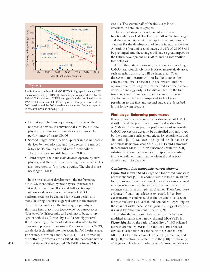
First stage: The basic operating principle of the
nanoscale devices is conventional CMOS, but new
physical phenomena in nanodevices enhance the
performance of nano-CMOS. Second stage: New function appears in the nanoscale
devices by new physics, and the devices are merged
into CMOS circuits to add new functionalities.
The operations are still based on CMOS. Third stage: The nanoscale devices operate by new
physics, and these devices operating by new principles
are integrated to form new circuits. The circuits are
no longer CMOS.
In the first stage of development, the performance
of CMOS is enhanced by new physical phenomena
that include quantum effects and ballistic transport
in nanoscale devices. Since the present CMOS
platform need not be changed for system design and
manufacturing, the first stage will come in the nearest
future. In the middle of the first stage, a paradigm
shift may take place from top-down-type nanodevices
(fabricated by lithography and etching) to bottom-up-
type nanodevices (formed by a self-assembly process).
If the operating principle of a device fabricated by the
bottom-up process is the same as for conventional CMOS,
this device is classified into the second half of the first stage.
For example, carbon nanotube (CNT) FETs, formed by
the bottom-up process, are classified into the second half of
the first stage if the integrated CNT-FETs form CMOS
circuits. The second half of the first stage is not
described in detail in this paper.
The second stage of development adds new
functionalities in CMOS. The last half of the first stage
and the second stage will overlap in time, and they will
compete for the development of future integrated devices.
At both the first and second stages, the life of CMOS will
be prolonged, and these stages will have a great impact on
the future development of CMOS and all information
technologies.
At the third stage, however, the circuits are no longer
CMOS, and completely new types of nanoscale devices,
such as spin transistors, will be integrated. Then,
the system architecture will not be the same as the
conventional one. Therefore, in the present authors’
opinion, the third stage will be realized as a mainstream
device technology only in the distant future; the first
two stages are of much more importance for current
developments. Actual examples of technologies
pertaining to the first and second stages are described
in the following sections.
First stage: Enhancing performanceIf new physics can enhance the performance of CMOS,
it will exceed the performance limit and scaling limit
of CMOS. For example, the performance of nanoscale
CMOS devices can actually be controlled and improved
by the quantum confinement effect. By experiments and
simulation [8–11], we have investigated the characteristics
of nanoscale narrow-channel MOSFETs and nanoscale
thin-channel MOSFETS on silicon-on-insulator (SOI)
substrates, where the carriers are respectively confined
into a one-dimensional narrow channel and a two-
dimensional thin channel.
Confinement into nanoscale narrow channel
Figure 2(a) shows a SEM image of a fabricated nanoscale
narrow channel [8]. The channel width is less than 10 nm.
In the nanoscale narrow channel, the carriers are confined
in a one-dimensional channel, and the confinement is
stronger than in a thin, planar channel. Therefore, more
evidence of quantum effects is expected. It has been
experimentally confirmed that the threshold voltage of
narrow MOSFETs is varied and controlled depending on
the channel width because the ground energy of carriers
is raised by quantum confinement [8, 9].
It is also shown by simulation that the mobility is
modified in nanoscale narrow-channel MOSFETs [9].
Figure 2(b) shows the ratio of mobility of [100]-oriented
narrow-channel MOSFETs to that of [110]-oriented
devices as a function of channel width. Conventional
MOSFETs have the channel in the [110] direction, and
the [100] direction is rotated from the [110] direction by
45 degrees. This larger mobility in [100]-oriented devices
Figure 1
Prediction of gate length of MOSFETs in high-performance (HP) microprocessors by ITRS [1]. Technology nodes predicted by the 1994–2003 versions of ITRS and gate lengths predicted by the 1999–2003 versions of ITRS are plotted. The predictions of the 2001 version and the 2003 version are the same. Devices reported in research are also shown [2, 7].
19941997
19992001
2003
1999
20012003
Research [2]
Research [7]
Technology node
Gate length ofmicroprocessor
400
200
1008060
40
20
1086
41994 1998 2002 2006 2010 2014 2018
Year of first product shipment
Tech
nolo
gy n
ode,
gat
e le
ngth
(nm
)
T. HIRAMOTO ET AL. IBM J. RES. & DEV. VOL. 50 NO. 4/5 JULY/SEPTEMBER 2006
412

is due to the anisotropic effective mass of silicon. In an
n-type MOSFET, this mobility enhancement is explained
by the electron population of valleys in the conduction
band.
Figure 2(c) shows the conduction-band structure
in [110]- and [100]-oriented channels. Owing to the
anisotropy of the electron mass, the rise of valley energy
is different depending on the direction of the ultranarrow
channel. In the [110]-oriented ultranarrow channel, six
equivalent valleys split into two sets of valleys: twofold
degenerate valleys and fourfold degenerate valleys. When
the channel width becomes narrower, the energy of the
twofold degenerate valleys increases more than that of the
fourfold degenerate valleys; therefore, more electrons are
populated in the latter. However, fourfold degenerate
valleys have larger mass and smaller mobility along the
[110] direction than twofold degenerate valleys, as shown
in Figure 2(c). Accordingly, the total electron mobility of
[110]-oriented narrow-channel MOSFETs is smaller [9].
In the [100]-oriented narrow channel, on the other
hand, six equivalent valleys split into three sets of twofold
degenerate valleys, as shown in Figure 2(c). Most of the
electrons are populated in the valley shown in red because
the energy of this valley is the smallest, and this valley has
the smallest mass and the highest mobility. For this
reason, [100]-oriented narrow-channel MOSFETs have
higher total mobility than [110]-oriented narrow-channel
MOSFETs [9]. This performance enhancement is scalable
because when the device becomes smaller, more quantum
confinement takes place and mobility is increased.
Confinement into nanoscale thin channel
In nanoscale thin-channel devices, the confinement of
carriers is weak compared with the confinement into
nanoscale narrow channels because the carriers can
have two degrees of freedom. Moreover, the transport
properties in a two-dimensional electron gas of a
quantum well in silicon [12] or in GaAs [13] have already
been investigated in detail at very low temperatures.
However, we have found experimentally that the hole
mobility is largely enhanced in an ultrathin-channel
silicon-on-insulator (SOI) MOSFET at room temperature
due to quantum confinement when the substrate crystal
orientation is (110) [10, 11]. This is one of the best
examples of the first stage.
Figure 3(a) shows a schematic structure of fabricated
SOI p-MOS devices [10]. The crystal orientation of silicon
on the buried oxide, or SOI, is (110) and the channel
direction is [110]. The silicon thickness is in the range of
3 nm. The TEM images of the gate oxide/silicon/buried
oxide from fabricated devices are shown in Figure 3(b).
The silicon thickness of the source and drain regions is
kept thicker by using a local oxidation technique in order
to make the parasitic resistance negligible. Figure 4(a)
shows the measured hole mobility as a function of silicon
Figure 2
(a) SEM image of nanoscale narrow channel. The narrow channel with width of less than 10 nm is formed between source and drain. Adapted from [8] with permission; ©2000 IEEE. (b) Simulated mobility ratio of [100]-oriented channel to [110]-oriented channel as a function of channel width. (c) Conduction band structure in [110]-oriented and [100]-oriented nanoscale narrow channels. Parts (b) and (c) adapted from [9] with permission; ©2001 IEEE.
(a)
(c)
231 nmSource
Drain2
Car
rier
mob
ilit
y ra
tio
( [1
00]
/ [11
0] )
Channel width (nm)(b)
4
3
2
1
00 2 4 6 8 10 12 14 16 18 20
tSOI 10 nm
Hole
Electron
Medium mobilityLow population
Medium mobilityLow population
Lowest mobilityLow population
Highest mobilityHighest population
Medium mobilityHigh population
[110]
[100]
[100]
[110]
[100]
IBM J. RES. & DEV. VOL. 50 NO. 4/5 JULY/SEPTEMBER 2006 T. HIRAMOTO ET AL.
413
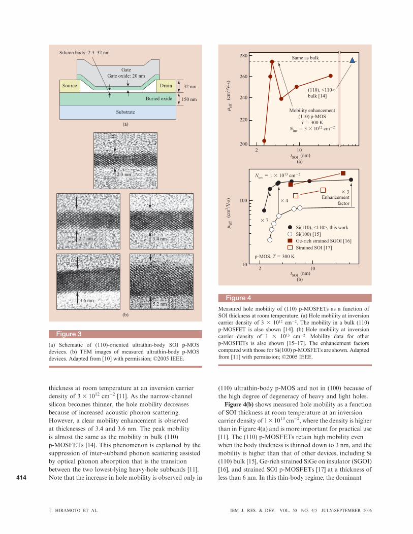
thickness at room temperature at an inversion carrier
density of 3 3 1012 cm2 [11]. As the narrow-channel
silicon becomes thinner, the hole mobility decreases
because of increased acoustic phonon scattering.
However, a clear mobility enhancement is observed
at thicknesses of 3.4 and 3.6 nm. The peak mobility
is almost the same as the mobility in bulk (110)
p-MOSFETs [14]. This phenomenon is explained by the
suppression of inter-subband phonon scattering assisted
by optical phonon absorption that is the transition
between the two lowest-lying heavy-hole subbands [11].
Note that the increase in hole mobility is observed only in
(110) ultrathin-body p-MOS and not in (100) because of
the high degree of degeneracy of heavy and light holes.
Figure 4(b) shows measured hole mobility as a function
of SOI thickness at room temperature at an inversion
carrier density of 131013 cm2, where the density is higher
than in Figure 4(a) and is more important for practical use
[11]. The (110) p-MOSFETs retain high mobility even
when the body thickness is thinned down to 3 nm, and the
mobility is higher than that of other devices, including Si
(110) bulk [15], Ge-rich strained SiGe on insulator (SGOI)
[16], and strained SOI p-MOSFETs [17] at a thickness of
less than 6 nm. In this thin-body regime, the dominant
Figure 3
(a) Schematic of (110)-oriented ultrathin-body SOI p-MOS devices. (b) TEM images of measured ultrathin-body p-MOS devices. Adapted from [10] with permission; ©2005 IEEE.
32 nm
150 nm
Silicon body: 2.3–32 nm
GateGate oxide: 20 nm
Substrate
(a)
2.3 nm
2.7 nm
3.6 nm5.2 nm
3.4 nm
(b)
Buried oxide
Source Drain
Figure 4
Measured hole mobility of (110) p-MOSFETs as a function of SOI thickness at room temperature. (a) Hole mobility at inversion carrier density of 3 1012 cm2. The mobility in a bulk (110) p-MOSFET is also shown [14]. (b) Hole mobility at inversion carrier density of 1 1013 cm2. Mobility data for other p-MOSFETs is also shown [15–17]. The enhancement factors compared with those for Si(100) p-MOSFETs are shown. Adapted from [11] with permission; ©2005 IEEE.
280
260
240
220
200
Same as bulk
eff
(cm
2 /V
-s)
2 10
(110), <110>bulk [14]
Mobility enhancement(110) p-MOS
T 300 KNinv 3 1012 cm2
tSOI (nm)(a)
2 10tSOI (nm)
(b)
ef
f (
cm2 /
V-s
)
~~~ ~
100
10
Si(110), <110>, this workSi(100) [15]Ge-rich strained SGOI [16]Strained SOI [17]
7
4
3Enhancement
factor
Ninv 1 1013 cm2
p-MOS, T 300 K
T. HIRAMOTO ET AL. IBM J. RES. & DEV. VOL. 50 NO. 4/5 JULY/SEPTEMBER 2006
414
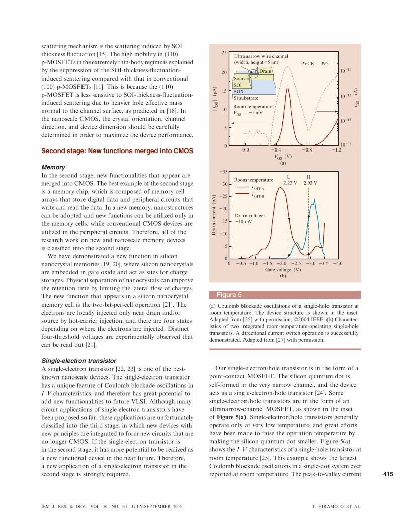
scattering mechanism is the scattering induced by SOI
thickness fluctuation [15]. The high mobility in (110)
p-MOSFETs in the extremely thin-body regime is explained
by the suppression of the SOI-thickness-fluctuation-
induced scattering compared with that in conventional
(100) p-MOSFETs [11]. This is because the (110)
p-MOSFET is less sensitive to SOI-thickness-fluctuation-
induced scattering due to heavier hole effective mass
normal to the channel surface, as predicted in [18]. In
the nanoscale CMOS, the crystal orientation, channel
direction, and device dimension should be carefully
determined in order to maximize the device performance.
Second stage: New functions merged into CMOS
Memory
In the second stage, new functionalities that appear are
merged into CMOS. The best example of the second stage
is a memory chip, which is composed of memory cell
arrays that store digital data and peripheral circuits that
write and read the data. In a new memory, nanostructures
can be adopted and new functions can be utilized only in
the memory cells, while conventional CMOS devices are
utilized in the peripheral circuits. Therefore, all of the
research work on new and nanoscale memory devices
is classified into the second stage.
We have demonstrated a new function in silicon
nanocrystal memories [19, 20], where silicon nanocrystals
are embedded in gate oxide and act as sites for charge
storages. Physical separation of nanocrystals can improve
the retention time by limiting the lateral flow of charges.
The new function that appears in a silicon nanocrystal
memory cell is the two-bit-per-cell operation [21]. The
electrons are locally injected only near drain and/or
source by hot-carrier injection, and there are four states
depending on where the electrons are injected. Distinct
four-threshold voltages are experimentally observed that
can be read out [21].
Single-electron transistor
A single-electron transistor [22, 23] is one of the best-
known nanoscale devices. The single-electron transistor
has a unique feature of Coulomb blockade oscillations in
I–V characteristics, and therefore has great potential to
add new functionalities to future VLSI. Although many
circuit applications of single-electron transistors have
been proposed so far, these applications are unfortunately
classified into the third stage, in which new devices with
new principles are integrated to form new circuits that are
no longer CMOS. If the single-electron transistor is
in the second stage, it has more potential to be realized as
a new functional device in the near future. Therefore,
a new application of a single-electron transistor in the
second stage is strongly required.
Our single-electron/hole transistor is in the form of a
point-contact MOSFET. The silicon quantum dot is
self-formed in the very narrow channel, and the device
acts as a single-electron/hole transistor [24]. Some
single-electron/hole transistors are in the form of an
ultranarrow-channel MOSFET, as shown in the inset
of Figure 5(a). Single-electron/hole transistors generally
operate only at very low temperature, and great efforts
have been made to raise the operation temperature by
making the silicon quantum dot smaller. Figure 5(a)
shows the I–V characteristics of a single-hole transistor at
room temperature [25]. This example shows the largest
Coulomb blockade oscillations in a single-dot system ever
reported at room temperature. The peak-to-valley current
Figure 5
(a) Coulomb blockade oscillations of a single-hole transistor at room temperature. The device structure is shown in the inset. Adapted from [25] with permission; ©2004 IEEE. (b) Character-istics of two integrated room-temperature-operating single-hole transistors. A directional current switch operation is successfully demonstrated. Adapted from [27] with permission.
0.0 0.4 0.8 1.2VGS (V)
(a)
| ID
S |
(pA
)
1014
1013
1012
1011
| ID
S |
(A)
BOXSi substrate
SOI
Ultranarrow wire channel(width, height <5 nm)
Source
Room temperatureVDS 1 mV
Drain
PVCR 395
ISHT-A
ISHT-B
Dra
in c
urre
nt (
pA)
Gate voltage (V)(b)
Room temperatureL
2.22 VH
2.93 V
Drain voltage:10 mV
4.03.53.02.52.01.51.00.50
0
5
10
15
20
25
35
30
25
20
15
10
5
0
IBM J. RES. & DEV. VOL. 50 NO. 4/5 JULY/SEPTEMBER 2006 T. HIRAMOTO ET AL.
415
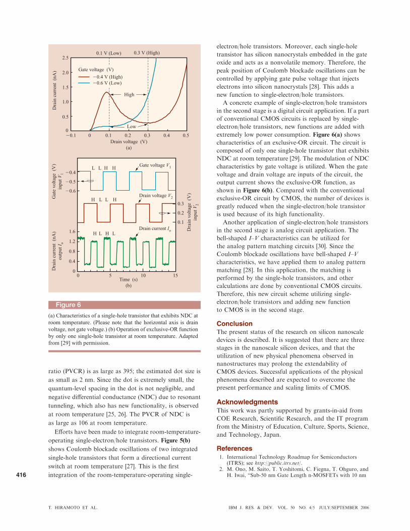
ratio (PVCR) is as large as 395; the estimated dot size is
as small as 2 nm. Since the dot is extremely small, the
quantum-level spacing in the dot is not negligible, and
negative differential conductance (NDC) due to resonant
tunneling, which also has new functionality, is observed
at room temperature [25, 26]. The PVCR of NDC is
as large as 106 at room temperature.
Efforts have been made to integrate room-temperature-
operating single-electron/hole transistors. Figure 5(b)
shows Coulomb blockade oscillations of two integrated
single-hole transistors that form a directional current
switch at room temperature [27]. This is the first
integration of the room-temperature-operating single-
electron/hole transistors. Moreover, each single-hole
transistor has silicon nanocrystals embedded in the gate
oxide and acts as a nonvolatile memory. Therefore, the
peak position of Coulomb blockade oscillations can be
controlled by applying gate pulse voltage that injects
electrons into silicon nanocrystals [28]. This adds a
new function to single-electron/hole transistors.
A concrete example of single-electron/hole transistors
in the second stage is a digital circuit application. If a part
of conventional CMOS circuits is replaced by single-
electron/hole transistors, new functions are added with
extremely low power consumption. Figure 6(a) shows
characteristics of an exclusive-OR circuit. The circuit is
composed of only one single-hole transistor that exhibits
NDC at room temperature [29]. The modulation of NDC
characteristics by gate voltage is utilized. When the gate
voltage and drain voltage are inputs of the circuit, the
output current shows the exclusive-OR function, as
shown in Figure 6(b). Compared with the conventional
exclusive-OR circuit by CMOS, the number of devices is
greatly reduced when the single-electron/hole transistor
is used because of its high functionality.
Another application of single-electron/hole transistors
in the second stage is analog circuit application. The
bell-shaped I–V characteristics can be utilized for
the analog pattern matching circuits [30]. Since the
Coulomb blockade oscillations have bell-shaped I–V
characteristics, we have applied them to analog pattern
matching [28]. In this application, the matching is
performed by the single-hole transistors, and other
calculations are done by conventional CMOS circuits.
Therefore, this new circuit scheme utilizing single-
electron/hole transistors and adding new function
to CMOS is in the second stage.
ConclusionThe present status of the research on silicon nanoscale
devices is described. It is suggested that there are three
stages in the nanoscale silicon devices, and that the
utilization of new physical phenomena observed in
nanostructures may prolong the extendability of
CMOS devices. Successful applications of the physical
phenomena described are expected to overcome the
present performance and scaling limits of CMOS.
AcknowledgmentsThis work was partly supported by grants-in-aid from
COE Research, Scientific Research, and the IT program
from the Ministry of Education, Culture, Sports, Science,
and Technology, Japan.
References1. International Technology Roadmap for Semiconductors
(ITRS); see http://public.itrs.net/.2. M. Ono, M. Saito, T. Yoshitomi, C. Fiegna, T. Ohguro, and
H. Iwai, ‘‘Sub-50 nm Gate Length n-MOSFETs with 10 nm
Figure 6
(a) Characteristics of a single-hole transistor that exhibits NDC at room temperature. (Please note that the horizontal axis is drain voltage, not gate voltage.) (b) Operation of exclusive-OR function by only one single-hole transistor at room temperature. Adapted from [29] with permission.
0.1 0 0.1 0.2 0.3 0.4 0.5
0.4 V (High) 0.6 V (Low)
Gate voltage (V)
Drain voltage (V)(a)
0.1 V (Low) 0.3 V (High)
High
Low0
0.5
1.0
1.5
2.0
2.5
0.4
0.5
0.6
1.6
1.2
0.8
0.4
0
0.3
0.2
0.1
0 5 10 15Time (s)
(b)
Dra
in v
olta
ge (
V)
inpu
t V2
Dra
in c
urre
nt (
nA)
Gat
e vo
ltage
(V
)in
put V
1
Dra
in c
urre
nt (
nA)
outp
ut I
o
L L H H
H L L H
H L H LDrain current Io
Drain voltage V2
Gate voltage V1
T. HIRAMOTO ET AL. IBM J. RES. & DEV. VOL. 50 NO. 4/5 JULY/SEPTEMBER 2006
416
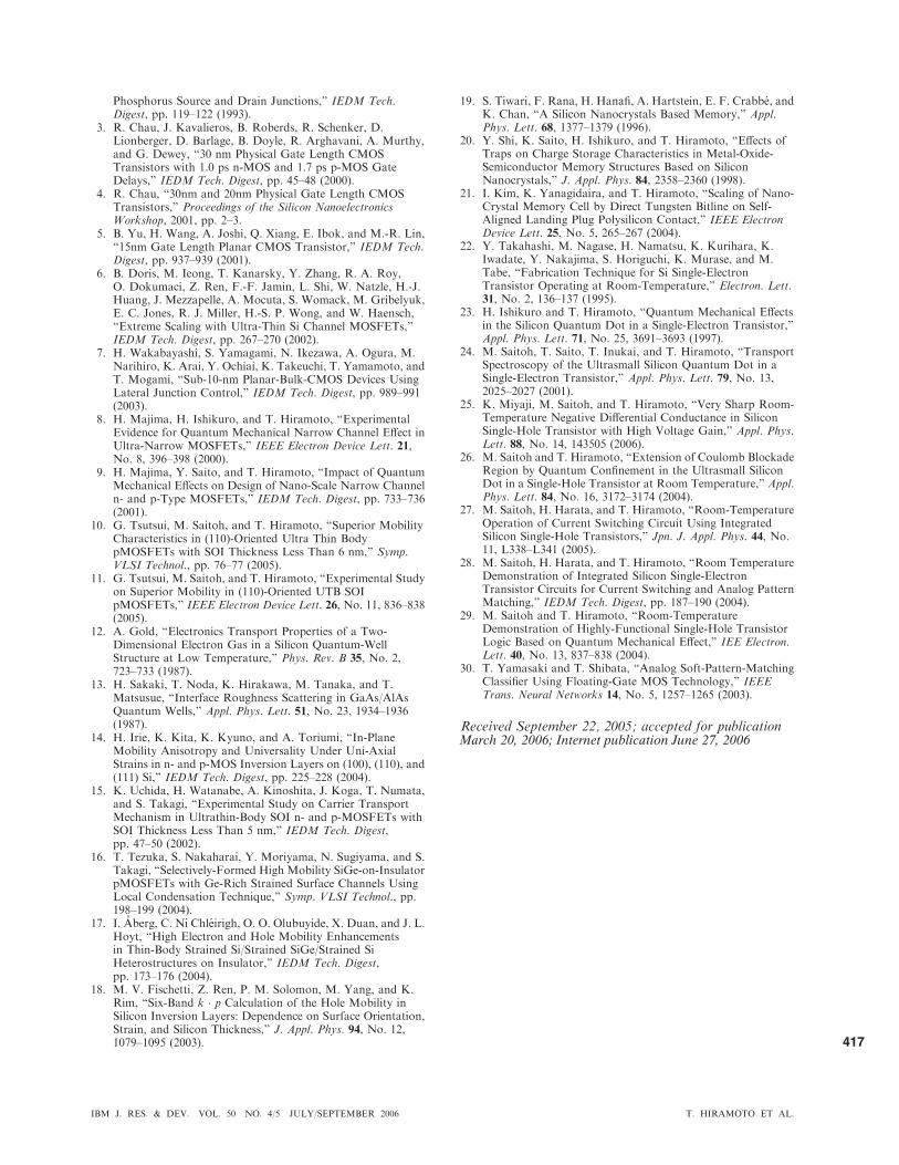
Phosphorus Source and Drain Junctions,’’ IEDM Tech.Digest, pp. 119–122 (1993).
3. R. Chau, J. Kavalieros, B. Roberds, R. Schenker, D.Lionberger, D. Barlage, B. Doyle, R. Arghavani, A. Murthy,and G. Dewey, ‘‘30 nm Physical Gate Length CMOSTransistors with 1.0 ps n-MOS and 1.7 ps p-MOS GateDelays,’’ IEDM Tech. Digest, pp. 45–48 (2000).
4. R. Chau, ‘‘30nm and 20nm Physical Gate Length CMOSTransistors,’’ Proceedings of the Silicon NanoelectronicsWorkshop, 2001, pp. 2–3.
5. B. Yu, H. Wang, A. Joshi, Q. Xiang, E. Ibok, and M.-R. Lin,‘‘15nm Gate Length Planar CMOS Transistor,’’ IEDM Tech.Digest, pp. 937–939 (2001).
6. B. Doris, M. Ieong, T. Kanarsky, Y. Zhang, R. A. Roy,O. Dokumaci, Z. Ren, F.-F. Jamin, L. Shi, W. Natzle, H.-J.Huang, J. Mezzapelle, A. Mocuta, S. Womack, M. Gribelyuk,E. C. Jones, R. J. Miller, H.-S. P. Wong, and W. Haensch,‘‘Extreme Scaling with Ultra-Thin Si Channel MOSFETs,’’IEDM Tech. Digest, pp. 267–270 (2002).
7. H. Wakabayashi, S. Yamagami, N. Ikezawa, A. Ogura, M.Narihiro, K. Arai, Y. Ochiai, K. Takeuchi, T. Yamamoto, andT. Mogami, ‘‘Sub-10-nm Planar-Bulk-CMOS Devices UsingLateral Junction Control,’’ IEDM Tech. Digest, pp. 989–991(2003).
8. H. Majima, H. Ishikuro, and T. Hiramoto, ‘‘ExperimentalEvidence for Quantum Mechanical Narrow Channel Effect inUltra-Narrow MOSFETs,’’ IEEE Electron Device Lett. 21,No. 8, 396–398 (2000).
9. H. Majima, Y. Saito, and T. Hiramoto, ‘‘Impact of QuantumMechanical Effects on Design of Nano-Scale Narrow Channeln- and p-Type MOSFETs,’’ IEDM Tech. Digest, pp. 733–736(2001).
10. G. Tsutsui, M. Saitoh, and T. Hiramoto, ‘‘Superior MobilityCharacteristics in (110)-Oriented Ultra Thin BodypMOSFETs with SOI Thickness Less Than 6 nm,’’ Symp.VLSI Technol., pp. 76–77 (2005).
11. G. Tsutsui, M. Saitoh, and T. Hiramoto, ‘‘Experimental Studyon Superior Mobility in (110)-Oriented UTB SOIpMOSFETs,’’ IEEE Electron Device Lett. 26, No. 11, 836–838(2005).
12. A. Gold, ‘‘Electronics Transport Properties of a Two-Dimensional Electron Gas in a Silicon Quantum-WellStructure at Low Temperature,’’ Phys. Rev. B 35, No. 2,723–733 (1987).
13. H. Sakaki, T. Noda, K. Hirakawa, M. Tanaka, and T.Matsusue, ‘‘Interface Roughness Scattering in GaAs/AlAsQuantum Wells,’’ Appl. Phys. Lett. 51, No. 23, 1934–1936(1987).
14. H. Irie, K. Kita, K. Kyuno, and A. Toriumi, ‘‘In-PlaneMobility Anisotropy and Universality Under Uni-AxialStrains in n- and p-MOS Inversion Layers on (100), (110), and(111) Si,’’ IEDM Tech. Digest, pp. 225–228 (2004).
15. K. Uchida, H. Watanabe, A. Kinoshita, J. Koga, T. Numata,and S. Takagi, ‘‘Experimental Study on Carrier TransportMechanism in Ultrathin-Body SOI n- and p-MOSFETs withSOI Thickness Less Than 5 nm,’’ IEDM Tech. Digest,pp. 47–50 (2002).
16. T. Tezuka, S. Nakaharai, Y. Moriyama, N. Sugiyama, and S.Takagi, ‘‘Selectively-Formed High Mobility SiGe-on-InsulatorpMOSFETs with Ge-Rich Strained Surface Channels UsingLocal Condensation Technique,’’ Symp. VLSI Technol., pp.198–199 (2004).
17. I. Aberg, C. Nı Chleirigh, O. O. Olubuyide, X. Duan, and J. L.Hoyt, ‘‘High Electron and Hole Mobility Enhancementsin Thin-Body Strained Si/Strained SiGe/Strained SiHeterostructures on Insulator,’’ IEDM Tech. Digest,pp. 173–176 (2004).
18. M. V. Fischetti, Z. Ren, P. M. Solomon, M. Yang, and K.Rim, ‘‘Six-Band k p Calculation of the Hole Mobility inSilicon Inversion Layers: Dependence on Surface Orientation,Strain, and Silicon Thickness,’’ J. Appl. Phys. 94, No. 12,1079–1095 (2003).
19. S. Tiwari, F. Rana, H. Hanafi, A. Hartstein, E. F. Crabbe, andK. Chan, ‘‘A Silicon Nanocrystals Based Memory,’’ Appl.Phys. Lett. 68, 1377–1379 (1996).
20. Y. Shi, K. Saito, H. Ishikuro, and T. Hiramoto, ‘‘Effects ofTraps on Charge Storage Characteristics in Metal-Oxide-Semiconductor Memory Structures Based on SiliconNanocrystals,’’ J. Appl. Phys. 84, 2358–2360 (1998).
21. I. Kim, K. Yanagidaira, and T. Hiramoto, ‘‘Scaling of Nano-Crystal Memory Cell by Direct Tungsten Bitline on Self-Aligned Landing Plug Polysilicon Contact,’’ IEEE ElectronDevice Lett. 25, No. 5, 265–267 (2004).
22. Y. Takahashi, M. Nagase, H. Namatsu, K. Kurihara, K.Iwadate, Y. Nakajima, S. Horiguchi, K. Murase, and M.Tabe, ‘‘Fabrication Technique for Si Single-ElectronTransistor Operating at Room-Temperature,’’ Electron. Lett.31, No. 2, 136–137 (1995).
23. H. Ishikuro and T. Hiramoto, ‘‘Quantum Mechanical Effectsin the Silicon Quantum Dot in a Single-Electron Transistor,’’Appl. Phys. Lett. 71, No. 25, 3691–3693 (1997).
24. M. Saitoh, T. Saito, T. Inukai, and T. Hiramoto, ‘‘TransportSpectroscopy of the Ultrasmall Silicon Quantum Dot in aSingle-Electron Transistor,’’ Appl. Phys. Lett. 79, No. 13,2025–2027 (2001).
25. K. Miyaji, M. Saitoh, and T. Hiramoto, ‘‘Very Sharp Room-Temperature Negative Differential Conductance in SiliconSingle-Hole Transistor with High Voltage Gain,’’ Appl. Phys.Lett. 88, No. 14, 143505 (2006).
26. M. Saitoh and T. Hiramoto, ‘‘Extension of Coulomb BlockadeRegion by Quantum Confinement in the Ultrasmall SiliconDot in a Single-Hole Transistor at Room Temperature,’’ Appl.Phys. Lett. 84, No. 16, 3172–3174 (2004).
27. M. Saitoh, H. Harata, and T. Hiramoto, ‘‘Room-TemperatureOperation of Current Switching Circuit Using IntegratedSilicon Single-Hole Transistors,’’ Jpn. J. Appl. Phys. 44, No.11, L338–L341 (2005).
28. M. Saitoh, H. Harata, and T. Hiramoto, ‘‘Room TemperatureDemonstration of Integrated Silicon Single-ElectronTransistor Circuits for Current Switching and Analog PatternMatching,’’ IEDM Tech. Digest, pp. 187–190 (2004).
29. M. Saitoh and T. Hiramoto, ‘‘Room-TemperatureDemonstration of Highly-Functional Single-Hole TransistorLogic Based on Quantum Mechanical Effect,’’ IEE Electron.Lett. 40, No. 13, 837–838 (2004).
30. T. Yamasaki and T. Shibata, ‘‘Analog Soft-Pattern-MatchingClassifier Using Floating-Gate MOS Technology,’’ IEEETrans. Neural Networks 14, No. 5, 1257–1265 (2003).
Received September 22, 2005; accepted for publication
IBM J. RES. & DEV. VOL. 50 NO. 4/5 JULY/SEPTEMBER 2006 T. HIRAMOTO ET AL.
417
March 20, 2006; Internet publication June 27, 2006
Toshiro Hiramoto Institute of Industrial Science, Universityof Tokyo, 4-6-1 Komaba, Meguro-ku, Tokyo 153-8505, Japan. Dr.Hiramoto received B.S., M.S., and Ph.D degrees in electronicengineering from the University of Tokyo in 1984, 1986, and 1989,respectively. In 1989, he joined the Device Development Center,Hitachi Ltd., Ome, Japan, where he was engaged in the device andcircuit design of ultra-fast BiCMOS SRAMs. In 1994, he joined theInstitute of Industrial Science at the University of Tokyo, Japan, asan Associate Professor. He was also an Associate Professor in theVLSI Design and Education Center at the University of Tokyofrom 1996 to 2002. Dr. Hiramoto has been a Professor in theInstitute of Industrial Science at the University of Tokyo since2002. His research interests include the low-power and low-voltagedesign of advanced CMOS devices, SOI MOSFETs, device/circuitcooperation schemes for low-power VLSI, quantum effects innanoscale MOSFETs, and silicon single-electron transistors. Dr.Hiramoto is a member of the IEEE, the IEICE, and the JapanSociety of Applied Physics. He has been an Elected AdComMember of the IEEE Electron Devices Society since 2001. Heserved as the General Chair of the Silicon NanoelectronicsWorkshop in 2003, and as Program Chair in 1997, 1999, and 2001.He also served on the Program Subcommittee on IntegratedCircuits of the IEEE International Electron Devices Meeting(IEDM) in 1993 and 1994 and on the Program Subcommitteeon CMOS Devices of the IEDM in 2003 and 2004. Dr. Hiramotohas served on the Program Committee of the Symposium onVLSI Technology since 2001. He was the Subcommittee Chairof CMOS Devices of the IEDM in 2005.
Masumi Saitoh Institute of Industrial Science, University ofTokyo, 4-6-1 Komaba, Meguro-ku, Tokyo 153-8505, Japan. Dr.Saitoh received the B.S., M.S., and Ph.D. degrees in electronicsengineering from the University of Tokyo, Japan, in 2000, 2002,and 2005, respectively. In 2005 he joined the Toshiba Corporation,Yokohama, Japan. His research interests are in physics in siliconnanodevices and their applications.
Gen Tsutsui Institute of Industrial Science, University ofTokyo, 4-6-1 Komaba, Meguro-ku, Tokyo 153-8505, Japan. Dr.Tsutsui received the B.S. and M.S. degrees from HiroshimaUniversity, Japan, in 1999 and 2001, respectively, and the Ph.D.degree from the University of Tokyo, Japan, in 2005. In 2006he joined the NEC Electronics Corporation, Sagamihara, Japan.His primary research interest is in quantum effects in nanoscaleMOSFETs.
T. HIRAMOTO ET AL. IBM J. RES. & DEV. VOL. 50 NO. 4/5 JULY/SEPTEMBER 2006
418