Embed Size (px)
Citation preview
Vishay SiliconixSiC413
Document Number: 69057S09-2250-Rev. D, 26-Oct-09
www.vishay.com1
This document is subject to change without notice.THE PRODUCTS DESCRIBED HEREIN AND THIS DOCUMENT ARE SUBJECT TO SPECIFIC DISCLAIMERS, SET FORTH AT www.vishay.com/doc?91000
For technical questions, contact: [email protected]
End of Life. Last Available Purchase Date is 31-Dec-2014
microBUCK® SiC4134 A, 26 V Integrated Synchronous Buck Regulator
DESCRIPTIONThe SiC413 is an integrated, DC/DC power conversionsolution with built-in PWM-optimized high- and low-siden-channel MOSFETs and advanced PWM controller. TheSiC413 provides a quick and easy to use POL voltageregulation solution for a wide range of applications. VishaySiliconix’s Proprietary packaging technology is used tooptimize the power stage and minimize power lossesassociated with parasitic impedances and switching delays.The co-packaged Gen III TrenchFET power MOSFETdevices deliver higher efficiency than lateral DMOSmonolithic solutions.
FEATURES • Integrated PWM controller and Gen III
trench MOSFETs
• Quick and easy single chip converter • Integrated current sense
• Cycle by cycle over-current protection
• Built-In bootstrap diode • Output over-voltage protection
• Under voltage lockout
• Thermal shutdown • Soft start
• Break-before-make operation
• PowerCAD Simulation software available at www.vishay.com/power-ics/powercad-list/
• Material categorization: For definitions of compliance please see www.vishay.com/doc?99912
APPLICATIONS • LCD TV, set top box and DVD player
• Desktop PC and server
• Add-in graphics board • Memory, FPGA or µP device power supplies
• Point of load DC/DC conversion
• Telecom and networking equipment
TYPICAL APPLICATION
PRODUCT SUMMARY Input Voltage Range 4.75 V to 26 V
Output Voltage Range 0.6 V to 13.2 V
Operating Frequency 500 kHz
Continuous Output Current 4 A
Peak Efficiency 93 %
Highside/Lowside RDS_ON 35 m/19 m
Package SO-8
Figure 1 - Typical Application Circuit
Enable
VIN
VOController
BOOT
VSW
GN
D
FB
COMP
EN
VR
EG
VIN
1
2
3
4
5
67
8
SiC413
Vishay SiliconixSiC413
www.vishay.com2
Document Number: 69057S09-2250-Rev. D, 26-Oct-09
This document is subject to change without notice.THE PRODUCTS DESCRIBED HEREIN AND THIS DOCUMENT ARE SUBJECT TO SPECIFIC DISCLAIMERS, SET FORTH AT www.vishay.com/doc?91000
For technical questions, contact: [email protected]
End of Life. Last Available Purchase Date is 31-Dec-2014
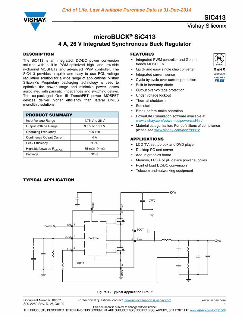
PIN CONFIGURATION
FUNCTIONAL BLOCK DIAGRAM
Figure 2. SO-8 Pin Out - Top View
1
2
3
4
8
7
6
5
FB
VIN
VREG
GNDVSW
BOOT
EN
COMP
PIN DESCRIPTION Pin Number Symbol Description
1 COMP Error amplifier output. Connects to the compensation network.
2 EN Chip enable pin. Active HIGH. Connects to a power source through a 10K to100K resistor to enable.
3 BOOT Connect to 0.1 µF capacitor from VSW to BOOT to power the high side gate driver.
4 VSWInductor Connection. Connect an output filter inductor to this pin. VSW is high impedance when the IC is in shutdown mode.
5 GND GROUND pin.
6 VIN Supply voltage.
7 VREG Internal regulator output. An external 4.7 µF decoupling capacitor is required at this pin.
8 FB Output voltage feedback input.
ORDERING INFORMATION Part Number Package
SiC413CB-T1-E3 SO-8 (6.2 x 5 x 1.75 mm)
SiC413DB Reference board
Figure 3. Functional Block Diagram
EN
UVLO
VIN
BOOT
GND
Control logicand activedead time
VSW
Shutdowncontrol
OTP
OVP
FB
VREG
PWM
GMFOSC
5.5 VREG
Overcurrent
COMP
VREG
Vishay SiliconixSiC413
Document Number: 69057S09-2250-Rev. D, 26-Oct-09
www.vishay.com3
This document is subject to change without notice.THE PRODUCTS DESCRIBED HEREIN AND THIS DOCUMENT ARE SUBJECT TO SPECIFIC DISCLAIMERS, SET FORTH AT www.vishay.com/doc?91000
For technical questions, contact: [email protected]
End of Life. Last Available Purchase Date is 31-Dec-2014
Notes: a. TA = 25 °C and all voltages referenced to GND unless otherwise noted.
Stresses beyond those listed under "Absolute Maximum Ratings" may cause permanent damage to the device. These are stress ratings only,and functional operation of the device at these or any other conditions beyond those indicated in the operational sections of the specifications isnot implied. Exposure to absolute maximum rating/conditions for extended periods may affect device reliability.
Notes: b. Recommended operating conditions are specified over the entire temperature range, and all voltages referenced to GND unless otherwise
noted. c. Peak value is specified for pulses 100 ns.
ABSOLUTE MAXIMUM RATINGS (TA = 25 °C, unless otherwise noted)a
Parameter Symbol Min. Max. Unit
Input Breakdown Voltage VIN - 0.3 28
VCommon Switch Node Breakdown Voltage
VSW DC - 1 28
VSW Peakc -1 30
Logic Inputs VCOMP, VFB, VEN - 0.3 6
Bootstrap Voltage VBOOT - 0.3 33
Maximum Power Dissipation PD 1.5 W
Operating Temperature Tj - 25 125
°CStorage Junction Temperature Tstg - 40 150
Soldering Peak Temperature 260
RECOMMENDED OPERATING CONDITIONSb Parameter Symbol Min. Typ. Max. Unit
Input Voltage VIN 4.75 12 26
VLogic Inputs
VCOMP, VFB, VEN
4.5 5 5.5
Common Switch NodeVSW DC - 0.3 12 26
VSW peakc - 0.3 24 28
THERMAL RESISTANCE RATINGS Parameter Symbol Typ. Unit
Junction-to-Case ResistanceIn Operation, Max. Junction RthJC
Contact Vishay for thermal design
assistance°C/W
Junction-to-Ambient ResistancePCB = Copper 25 mm x 25 mm RthJA
Case Top to Board EdgePCB = EVBSiC413 Rev. 3.0; No Forced Airflow RthCA
Vishay SiliconixSiC413
www.vishay.com4
Document Number: 69057S09-2250-Rev. D, 26-Oct-09
This document is subject to change without notice.THE PRODUCTS DESCRIBED HEREIN AND THIS DOCUMENT ARE SUBJECT TO SPECIFIC DISCLAIMERS, SET FORTH AT www.vishay.com/doc?91000
For technical questions, contact: [email protected]
End of Life. Last Available Purchase Date is 31-Dec-2014
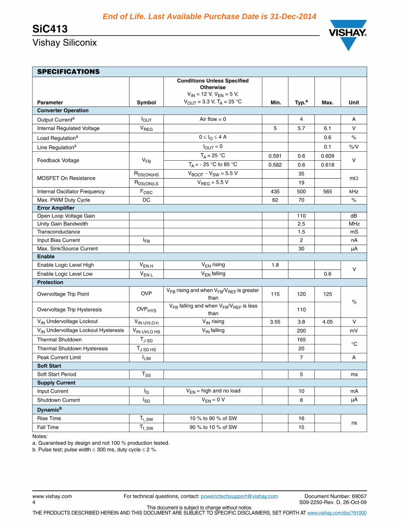
Notes:a. Guaranteed by design and not 100 % production tested.b. Pulse test; pulse width 300 ms, duty cycle 2 %.
SPECIFICATIONS
Parameter Symbol
Conditions Unless Specified Otherwise
VIN = 12 V, VEN = 5 V, VOUT = 3.3 V, TA = 25 °C Min. Typ.a Max. Unit
Converter Operation
Output Currenta IOUT Air flow = 0 4 A
Internal Regulated Voltage VREG 5 5.7 6.1 V
Load Regulationa 0 IO 4 A 0.6 %
Line Regulationa IOUT = 0 0.1 %/V
Feedback Voltage VFBTA = 25 °C 0.591 0.6 0.609
VTA = - 25 °C to 85 °C 0.582 0.6 0.618
MOSFET On ResistanceRDS(ON)HS VBOOT - VSW = 5.5 V 35
mRDS(ON)LS VREG = 5.5 V 19
Internal Oscillator Frequency FOSC 435 500 565 kHz
Max. PWM Duty Cycle DC 62 70 %
Error Amplifier
Open Loop Voltage Gain 110 dB
Unity Gain Bandwidth 2.5 MHz
Transconductance 1.5 mS
Input Bias Current IFB 2 nA
Max. Sink/Source Current 30 µA
Enable
Enable Logic Level High VEN H VEN rising 1.8V
Enable Logic Level Low VEN L VEN falling 0.6
Protection
Overvoltage Trip Point OVPVFB rising and when VFB/VREF is greater
than115 120 125
%
Overvoltage Trip Hysteresis OVPHYSVFB falling and when VFB/VREF is less
than110
VIN Undervoltage Lockout VIN UVLO-h VIN rising 3.55 3.8 4.05 V
VIN Undervoltage Lockout Hysteresis VIN UVLO HS VIN falling 200 mV
Thermal Shutdown TJ SD 165°C
Thermal Shutdown Hysteresis TJ SD HS 20
Peak Current Limit ILIM 7 A
Soft Start
Soft Start Period TSS 5 ms
Supply Current
Input Current IQ VEN = high and no load 10 mA
Shutdown Current ISD VEN = 0 V 8 µA
Dynamicb
Rise Time Tr_SW 10 % to 90 % of SW 16ns
Fall Time Tf_SW 90 % to 10 % of SW 15
Vishay SiliconixSiC413
Document Number: 69057S09-2250-Rev. D, 26-Oct-09
www.vishay.com5
This document is subject to change without notice.THE PRODUCTS DESCRIBED HEREIN AND THIS DOCUMENT ARE SUBJECT TO SPECIFIC DISCLAIMERS, SET FORTH AT www.vishay.com/doc?91000
For technical questions, contact: [email protected]
End of Life. Last Available Purchase Date is 31-Dec-2014
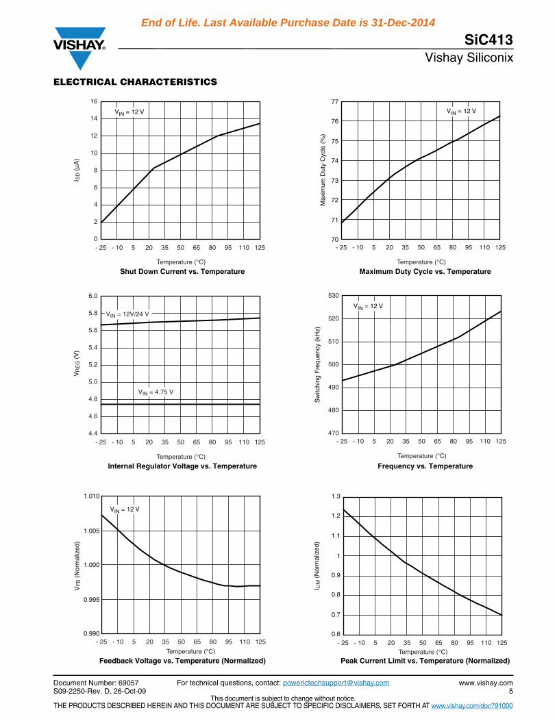
ELECTRICAL CHARACTERISTICS
Shut Down Current vs. Temperature
Internal Regulator Voltage vs. Temperature
Feedback Voltage vs. Temperature (Normalized)
I SD
(µA
)
0
2
4
6
8
10
12
14
16
- 25 - 10 5 20 35 50 65 80 95 110 125
Temperature (°C)
VIN = 12 V
VR
EG
(V
)
- 25 - 10 5 20 35 50 65 80 95 110 125
Temperature (°C)
4.4
4.6
4.8
5.0
5.2
5.4
5.6
5.8
6.0
VIN = 12V/24 V
VIN = 4.75 V
VF
B (
Nor
mal
ized
)
- 25 - 10 5 20 35 50 65 80 95 110 125
Temperature (°C)
0.990
0.995
1.000
1.005
1.010
VIN = 12 V
Maximum Duty Cycle vs. Temperature
Frequency vs. Temperature
Peak Current Limit vs. Temperature (Normalized)
- 25 - 10 5 20 35 50 65 80 95 110 125
Temperature (°C)
70
71
72
73
74
75
76
77
Max
imum
Dut
y C
ycle
(%
)
VIN = 12 V
Sw
itchi
ng F
requ
ency
(kH
z)
- 25 - 10 5 20 35 50 65 80 95 110 125
Temperature (°C)
470
480
490
500
510
520
530
VIN = 12 V
I LIM
(N
orm
aliz
ed)
- 25 - 10 5 20 35 50 65 80 95 110 125Temperature (°C)
0.6
0.7
0.8
0.9
1
1.1
1.2
1.3
Vishay SiliconixSiC413
www.vishay.com6
Document Number: 69057S09-2250-Rev. D, 26-Oct-09
This document is subject to change without notice.THE PRODUCTS DESCRIBED HEREIN AND THIS DOCUMENT ARE SUBJECT TO SPECIFIC DISCLAIMERS, SET FORTH AT www.vishay.com/doc?91000
For technical questions, contact: [email protected]
End of Life. Last Available Purchase Date is 31-Dec-2014
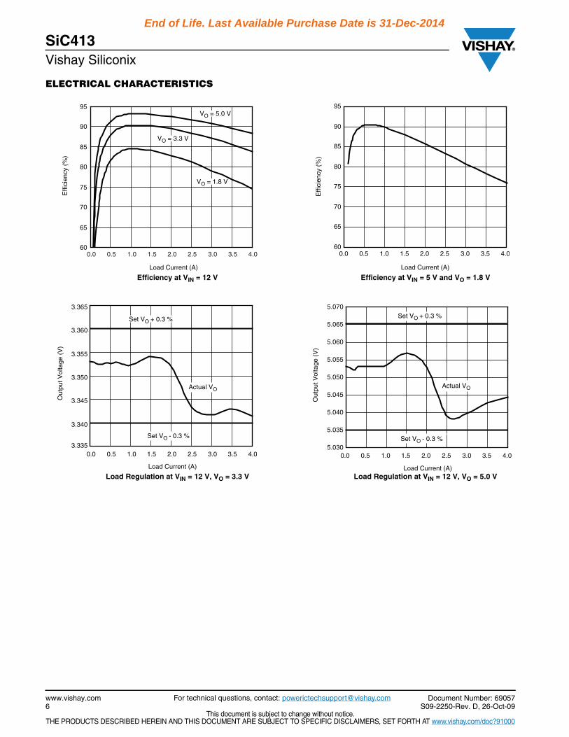
ELECTRICAL CHARACTERISTICS
Efficiency at VIN = 12 V
Load Regulation at VIN = 12 V, VO = 3.3 V
Load Current (A)
Effi
cien
cy (
%)
0.0 0.5 1.0 1.5 2.0 2.5 3.0 3.5 4.060
65
70
75
80
85
90
95VO = 5.0 V
VO = 3.3 V
VO = 1.8 V
Load Current (A)
Out
put V
olta
ge (
V)
0.0 0.5 1.0 1.5 2.0 2.5 3.0 3.5 4.03.335
3.340
3.345
3.350
3.355
3.360
3.365
Set VO - 0.3 %
Actual VO
Set VO + 0.3 %
Efficiency at VIN = 5 V and VO = 1.8 V
Load Regulation at VIN = 12 V, VO = 5.0 V
Load Current (A)
Effi
cien
cy (
%)
0.0 0.5 1.0 1.5 2.0 2.5 3.0 3.5 4.060
65
70
75
80
85
90
95
Load Current (A)
Out
put V
olta
ge (
V)
0.0 0.5 1.0 1.5 2.0 2.5 3.0 3.5 4.05.030
5.035
5.040
5.045
5.050
5.055
5.060
5.065
5.070
Set VO - 0.3 %
Set VO + 0.3 %
Actual VO
Vishay SiliconixSiC413
Document Number: 69057S09-2250-Rev. D, 26-Oct-09
www.vishay.com7
This document is subject to change without notice.THE PRODUCTS DESCRIBED HEREIN AND THIS DOCUMENT ARE SUBJECT TO SPECIFIC DISCLAIMERS, SET FORTH AT www.vishay.com/doc?91000
For technical questions, contact: [email protected]
End of Life. Last Available Purchase Date is 31-Dec-2014
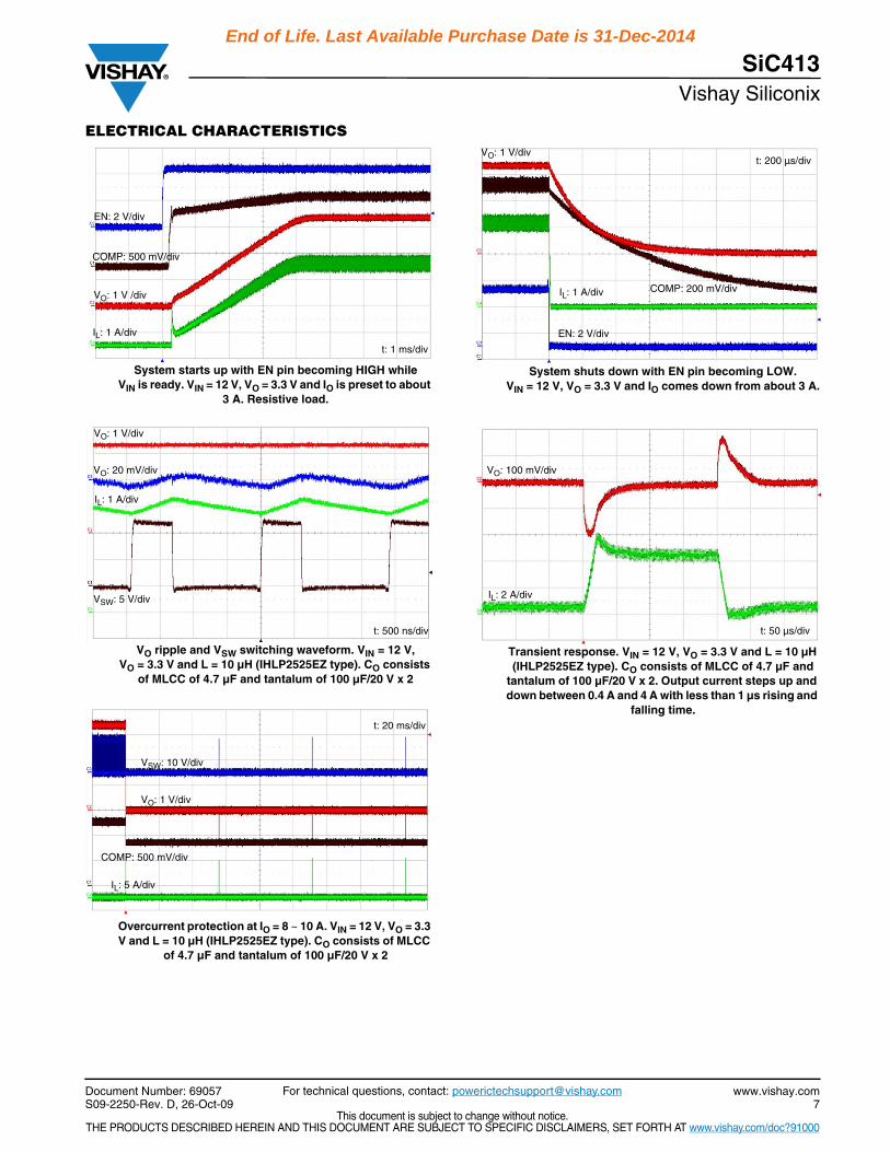
ELECTRICAL CHARACTERISTICS
System starts up with EN pin becoming HIGH while VIN is ready. VIN = 12 V, VO = 3.3 V and IO is preset to about
3 A. Resistive load.
VO ripple and VSW switching waveform. VIN = 12 V, VO = 3.3 V and L = 10 µH (IHLP2525EZ type). CO consists
of MLCC of 4.7 µF and tantalum of 100 µF/20 V x 2
Overcurrent protection at IO = 8 ~ 10 A. VIN = 12 V, VO = 3.3 V and L = 10 µH (IHLP2525EZ type). CO consists of MLCC
of 4.7 µF and tantalum of 100 µF/20 V x 2
COMP: 500 mV/div
VO: 1 V /div
EN: 2 V/div
IL: 1 A/div
t: 1 ms/div
VSW: 5 V/div
VO: 1 V/div
VO: 20 mV/div
IL: 1 A/div
t: 500 ns/div
COMP: 500 mV/div
IL: 5 A/div
VSW: 10 V/div
VO: 1 V/div
t: 20 ms/div
System shuts down with EN pin becoming LOW. VIN = 12 V, VO = 3.3 V and IO comes down from about 3 A.
Transient response. VIN = 12 V, VO = 3.3 V and L = 10 µH (IHLP2525EZ type). CO consists of MLCC of 4.7 µF and
tantalum of 100 µF/20 V x 2. Output current steps up and down between 0.4 A and 4 A with less than 1 µs rising and
falling time.
COMP: 200 mV/div
VO: 1 V/div
EN: 2 V/div
IL: 1 A/div
t: 200 µs/div
t: 50 µs/div
VO: 100 mV/div
IL: 2 A/div
Vishay SiliconixSiC413
www.vishay.com8
Document Number: 69057S09-2250-Rev. D, 26-Oct-09
This document is subject to change without notice.THE PRODUCTS DESCRIBED HEREIN AND THIS DOCUMENT ARE SUBJECT TO SPECIFIC DISCLAIMERS, SET FORTH AT www.vishay.com/doc?91000
For technical questions, contact: [email protected]
End of Life. Last Available Purchase Date is 31-Dec-2014
DETAILED OPERATIONAL DESCRIPTIONInput Voltage (VIN)The input voltage pin on the SiC413CB provides the biassupply for the PWM controller IC and the MOSFET drivercircuitry. This pin also is internally connected to the drain ofthe high side MOSFET.
Feedback (FB) and Output Voltage (VO)The FB pin is the negative input of the internal error amplifier.This pin connects to the center of the output voltage divider,through a 10K ~ 100K resistor (for noise isolation). When inregulation the FB voltage is 0.6 V. The output voltage VO isset based on the following formula.
VO = VREF (1 + R1/R2)
where R1 and R2 are shown in Figure 4.
Enable (EN)CMOS logic signal. In the low state, the EN pin shuts downthe driver IC and disables both high-side and low-sideMOSFETs. An internal pull up resistor will enable the deviceif this pin is left open. An external pull up of 10 k to 100 kis recommended for better noise immunity.
Soft-Start (SS)This device allows typical 5 ms soft start time to preventinrush current during system startup. The soft start cyclestarts when EN is asserted (low to high).
Under Voltage Lockout (UVLO)The SiC413CB incorporates an under voltage lockout circuitto keep the device disabled when the input voltage (VIN) isbelow x.xx V typical. During power up, internal circuits areheld inactive until VIN exceeds the nominal UVLO thresholdvoltage. Once the UVLO rising threshold is reached, thedevice start-up begins. The device keeps operating unlessVIN drops below UVLO falling threshold. The nominal200 mV UVLO hysteresis and 2.5 µs rising and falling edgede-glitch circuit reduce the likelihood of the device shutdowndue to noise on VIN.
Switch Node (VSW)The switch node is the interconnection between the andhigh- and low-side MOSFETs. Connect the output inductor tothis pin. Also, this node is the return path for the bootstrapcapacitor.
Bootstrap Circuit (BOOT)A diode and a capacitor form a bootstrap circuit that powershigh-side MOSFET driver. SiC413 has this diode built in andtherefore only an external capacitor is required to form thiscircuit. This capacitor is connected between BOOT pin andVSW pin.
Over Temperature Protection (OTP)OTP provides thermal protection to the controller and powerMOSFETs when an overload condition occurs. When thejunction temperature of the SiC413CB exceeds nominal 165°C (OTP trip point), the power MOSFETs will be turned off
and the controller will be disabled. The device willautomatically restart when the junction temperature dropsto nominal 20 °C below its trip point. After the thermalprotection is deasserted, a regular soft start cycle will beinitiated.
Over Voltage Protection (OVP)When the feedback voltage on FB pin exceeds 120 % ofVREF, the over voltage condition is asserted. When overvoltage occurs, the controller will turn on low-side MOSFETand turn off high-side MOSFET to discharge the excessiveoutput voltage. The over voltage condition is removed whenthe voltage on FB pin drops to below 110 % of VREF.
Over Current Protection (OCP)The SiC413CB integrates all components required for overcurrent protection. This achieved by sensing the currentflowing through the Low-side MOSFET. When low-sideMOSFET is turned on, the current flowing through it willgenerate a voltage drop determined by its RDS(ON). After ablanking time delay (to ignore switching noise), this voltageis compared to a reference that corresponds to a presetovercurrent threshold (typical 7 A peak). If the voltage dropon low-side MOSFET is higher than the preset reference, anovercurrent protection event occurs. This triggers the PWMcontroller to keep the low side MOSFET on until the inductorcurrent discharges to a level below the over currentprotection threshold. This lowers the duty cycle and causesthe output voltage to droop. The SiC413CB overcurrent fault mode is designed to protectagainst false triggering.An overcurrent event is defined asstarting when the overcurrent threshold is tripped and endingwhen the inductor current in the low side MOSFET is belowthe overcurrent trheshold. Seven sequential overcurrentevents are required to place the SiC413CB into the over cur-rent fault mode.Overcurrent events are counted by an up down counter. Ifthe overcurrent state is detected, the counter counts 1 upotherwise it counts 1 down. If the count reaches 7, the devicewill enter fault mode and both high- and low-side MOSFETswill turn off for 15 PWM clock cycles. After this period, thedevice will initiate a regular soft start. This sequence repeatsuntil the overcurrent is completely removed. This is oftenreferred to as hiccup mode. If the counter does not reach thecount of 7. The SiC413CB does not enter into the overcurrentfault mode and operation is not disrupted.
Shoot-Through Protection (Break-Before-Make: BBM)The SiC413CB has an internal break-before-make functionto ensure that both high- and low-side MOSFETs are notturned on at the same time.An internal circuit detects the falling edge of both high- andlow-side gate drive. The low-side MOSFET is turned on onlyafter the high-side gate voltage is less than VBBM, similarlythe high-side MOSFET gate is turned on after a fixed dead-time after the low side gate is less than VBBM. This Break-Before-Make time parameter is not user adjustable.
Vishay SiliconixSiC413
Document Number: 69057S09-2250-Rev. D, 26-Oct-09
www.vishay.com9
This document is subject to change without notice.THE PRODUCTS DESCRIBED HEREIN AND THIS DOCUMENT ARE SUBJECT TO SPECIFIC DISCLAIMERS, SET FORTH AT www.vishay.com/doc?91000
For technical questions, contact: [email protected]
End of Life. Last Available Purchase Date is 31-Dec-2014
APPLICATION NOTESInductor SelectionThe inductor is one of the energy storage components ina converter. Choosing an inductor means specifying itssize, structure, material, inductance, saturation level,DC-resistance (DCR), and core loss. Fortunately, there aremany inductor vendors that offer wide selections with amplespecifications and test data, such as Vishay Dale.The following are some key parameters that users shouldfocus on. In PWM mode, inductance has a direct impact onthe ripple current. Assuming 100 % efficiency, the steadystate peak-to-peak inductor (L) ripple current (IPP) can becalculated as
where f = switching frequency.
Higher inductance means lower ripple current, lower rmscurrent, lower voltage ripple on both input and output, andhigher efficiency, unless the resistive loss of the inductordominates the overall conduction loss. However, higherinductance also means a bigger inductor size and a slowerresponse to transients. For fixed line and load conditions,higher inductance results in a lower peak current for eachpulse, a lower load capability, and a higher switchingfrequency. The saturation level is another importantparameter in choosing inductors. Note that the saturationlevels specified in data sheets are maximum currents. For adc-to-dc converter operating in PWM mode, it is themaximum peak inductor (IPK) current that is relevant, andcan be calculated using these equations:
where IO = output current.This peak current varies with inductance tolerance and othererrors, and the rated saturation level varies overtemperature. So a sufficient design margin is required whenchoosing current ratings. A high-frequency core material,such as ferrite, should be chosen, the core loss could lead toserious efficiency penalties. The DCR should be kept as lowas possible to reduce conduction losses.
Input Capacitor SelectionTo minimize input voltage ripple caused by the step-downconversion, and interference of large voltage spikes fromother circuits, a low-ESR input capacitor is required to filterthe input voltage. The input capacitor should be rated for themaximum RMS input current of:
It is common practice to rate for the worst-case RMS ripplethat occurs when the duty cycle is at 50 %:
Output Capacitor SelectionThe output capacitor affects output voltage ripple due to2 reasons: the capacitance and the effective seriesresistance (ESR). The selection of the output capacitor isprimarily determined by the capacitor ESR requiredminimizing voltage ripple and current ripple. The relationshipbetween output ripple VO, capacitance CO and its ESR is:
Multiple capacitors placed in parallel may be needed to meetthe ESR requirements. However if the ESR is too low it maycause stability problems.
Control Loop DesignThe SiC413CB is an integrated voltage mode buckconverter. The loop stability depends on input and outputvoltage, output LC filter, the equivalent lumped capacitance,resistance and inductance attached to the output voltage railbeyond the LC filter. The output LC filter creates a two poleroll-off of the loop gain that makes the closed loop systeminherently unstable. Therefore, a compensation network ofpoles and zeros must be implemented to achieveunconditional stability. Figure 4 shows a simplified diagram of the SiC413CB buckconverter control loop and the external elements that affectloop gain, phase shift and stability. In this diagram L1, C4and C5 and R6 form a first order model of low pass filter.Resistor R6 represents the effective series resistance (ESR)of C5, which is often the case of a polymer (tantalum)capacitor. Ceramic (MLCC) capacitors are also used asdenoted by C4, which has near zero ESR. To balance theperformance and cost, the recommended output capacitorconfiguration is a combination of low cost, high capacitancepolymer capacitors (C5) with ESR (R6) to add a zero to helpboost phase margin and MLCC capacitors (C4) that have lowESR for achieving low voltage ripple. In practice, the lumpedequivalent capacitance at the output of the filter may be acombination of many different kinds of capacitors. Thecharacteristics of these capacitors must be considered whenderiving the open loop transfer function and designing theloop compensation. It is important to have a goodapproximation of the lumped impedance (capacitors,resistors, ferrite beads, filters, etc.) tied to the rail beforecalculating compensation network component values. Resistor R1 and R2 form the feedback voltage divider thatsamples the DC output and applies a feedback signal to theFB pin. Components C1, C2, C3, R4, R5 and thetransconductance error amplifier form the loopcompensation network. With voltage mode control loop the
( )fLVVVV
IIN
OINOPP ..
-.=
2PP
OPK
III +=
)( -=IN
O
IN
OMAXO.RMS
V
V
V
VII 1
2.MAX.O
RMSI
I =
)( ..+.=ΔO
PPOCf
ESRIV8
1
Vishay SiliconixSiC413
www.vishay.com10
Document Number: 69057S09-2250-Rev. D, 26-Oct-09
This document is subject to change without notice.THE PRODUCTS DESCRIBED HEREIN AND THIS DOCUMENT ARE SUBJECT TO SPECIFIC DISCLAIMERS, SET FORTH AT www.vishay.com/doc?91000
For technical questions, contact: [email protected]
End of Life. Last Available Purchase Date is 31-Dec-2014
output voltage is fed back at the FB pin. This feedback signalis summed with a precision voltage reference through a highbandwidth transconductance amplifier, often referred to asthe error amplifier. This summation creates an error signalthat is proportional to the difference between the actualoutput voltage and the desired output voltage, which isachieved when the voltage at the center tap of the feedbackresistor divider is equal to the voltage reference. The errorsignal is present at the COMP pin, which is the output of theerror amplifier. The error amplifier in the SiC413CB has a high loop gain anda 2.5 MHz Gain Bandwidth Product. It is designed this wayto provide fast transient response in applications such asDRAM memory arrays in Graphics Cards. This lets thecontrol loop quickly respond to any deviation of the outputvoltage. It also makes the SiC413CB more sensitive to noiseon the FB pin. It is recommended to add resistor R3 at 20 kto help isolate the error amplifier from noise on the FB pinand give the designer the full benefit of the fast responsetime the SiC413CB can deliver.Under normal operation the output of the error signal variesbetween 1.0 V and 2.0 V. This corresponds to the peak topeak amplitude of the saw-tooth wave form generated by theoscillator at the input to the PWM comparator. The PWMcomparator drives the logic that controls the MOSFET gatedrivers. These drivers control the turn on and turn off of thehigh- and low-side MOSFETs. As the error signal varies thePWM duty cycle is adjusted up and down to counteract theerror. This interaction is normal load modulation and can beseen in a slight jitter on the trailing edge of the PWM signal.The resulting PWM signal at the VSW switching node isintegrated by the LC filter to deliver the desired DC outputvoltage.Very low steady state duty cycles occur when the desiredoutput is much smaller than the input (i.e. 24 V input to 1.2 Voutput). In this case, the error signal will be closer to 1 V.Very high duty cycles occur when the desired output is closerto the input (i.e. 5 V input to 3.3 V output). In this case, theerror signal is closer to 2 V. As can be seen, in these casesthe error signal may have limited headroom for control undersevere load transient conditions. This can result anasymmetrical transient response characteristic and slightlylonger regulation recovery times for either the loadacquisition or load shedding.
Open Loop Transfer FunctionThe following discussion derives the equations for the openloop transfer function. The technique for selecting the polesand zeros for optimized loop stability is then presented.For this analysis we are considering the LC filterapproximation given in Figure 4 and are not considering theimpedance of the load. However, most output impedancescan be modeled using the lumped circuit approximationshown in Figure 4. One exception is the use of a filter witha roll off frequency that is inside the loop bandwidth. In thiscase, derivation of the transfer function that includes the
phase and gain effects of this filter is important. In somecases, filters can reduce gain margin and cause marginalstability if not considered thoroughly. The loop gain transfer function is broken into four blocks,each representing a different part of the buck converter. Thefour blocks and their frequency domain equations are asfollows:Block 1 - GLC: Output LC filter consisting of L1, C4, C5 andR6
Block 2 - GSP: Output voltage sampling network composedof C1, R1 and R2
Block 3 - GPWM: PWM modulation gain that equals toVIN/VOSC, where VOSC = saw tooth peak to peak voltage
Block 4 - GCOMP: Amplifier compensator with components ofC2, C3, R4, R5 and the amplifier gain gM, which is a functionof frequency.
Resistor R4 value should be very large compared to R5.The purpose of R4 is to eliminate non-monotonic outputbehavior during rapidly pulsed off-then-on line transients. R4provides a fast discharge path for C3 and resets the errorsignal at COMP to zero before the line input pulses back on.Ideally, R4 can be ignored for the purposes of the looptransfer function.Ignoring R4 gives the following simplified transfer function forBlock 4.
The overall open loop transfer function for this system, GOL,is then the product of the four transfer functions derived foreach block.
Converting to the logarithm form we have
SR6 • C5 + 123=
L1 • (C4 + C5) + SR6 • C5 + 1R6 • C4 • C5 • L1 + SSGLC
1
1
R1 + R2
R1 • R2S+
R1 • C1S+
GSP
• C1
=
OSC
IN
PWM
VG ΔV
=
1)
111
11
2
R4 • R5 • C2 • C3R5 • C3 R4 • C3 R5 • C2 S
R5 • C2 S +
C3gG MCOMP
++++ S (
••=
1
1
C2 + C3
C2 • C3R5 •
S+
R5 • C2S+
SC3
gG
MCOMP •=
GOL = GLC • GSP • GPWM • GCOMP
GOL (dB) = G LC (dB) + GSP(dB) + GPWM (dB) + G COMP (dB)
Vishay SiliconixSiC413
Document Number: 69057S09-2250-Rev. D, 26-Oct-09
www.vishay.com11
This document is subject to change without notice.THE PRODUCTS DESCRIBED HEREIN AND THIS DOCUMENT ARE SUBJECT TO SPECIFIC DISCLAIMERS, SET FORTH AT www.vishay.com/doc?91000
For technical questions, contact: [email protected]
End of Life. Last Available Purchase Date is 31-Dec-2014
Compensation ConsiderationsThe criterion for unconditional stability of a closed loopsystem is that the open loop transfer function has thefollowing attributes. 1. The magnitude of the open loop transfer function must
cross through 0 dB with a slope of - 20 dB per decade2. The phase shift of the open loop transfer function must be
at least 45 at the frequency, at which the magnitude of theloop gain crosses through 0 dB
3. The phase shift should not be rapidly decreasing at loopgain slightly less than 0 dB
To determine if these criterion are met the Bode plot of thetransfer function is drawn. Before drawing the bode plot, thepoles and zeros need to be located. The following discussionserves as a guide to selection of the component values forthe compensation network.The compensation process begins by selecting loopbandwidth. We recommend that the 0 dB crossoverfrequency is set somewhere between 10 % and 20 % ofswitching frequency. The SiC413CB has a fixed switchingfrequency of 500 kHz. This means that the bandwidth of theloop can be set somewhere between 50 kHz and 100 kHz.This wide loop bandwidth, made possible by the ultra fasterror amplifier in the SiC413CB, can provide excellenttransient response and load regulation.It can be seen that within the LC filter block, there aregenerally three poles (denoted P1, P2 and P3) and one zero(denoted Z1). The double pole (P1 and P2) created by theLC filter is the dominant response characteristic of thesystem. The locations of these poles and zero dependstrongly on the types of capacitors used in the output filter.Three cases will be analyzed as follows.Case 1: Output capacitors are a combination of those withESR (C5. e.g. polymer or tantalum type) and those with noESR or little ESR (C4. e.g. ceramic type)The poles and zero for this case are as follows
To meet the above stability criterion, the frequency of thezero fZ1 should be placed at a frequency lower than or equalto that at the double pole of fP1,P2. Pole fP3 should be locatedat a much higher frequency than fP1,P2. This requirementsets the boundaries on the values of C4, C5 and R6.Capacitor C4 has to be much smaller than C5.Case 2: Output capacitor is all ceramic MLCCIgnoring C5 and R6, the poles are as follows
This output filter configuration can be challenging becausethere is no zero to help boost the phase shift that isintroduced by the LC double pole.Case 3: All capacitors have ESR, no ceramics.Ignoring C4 we have the following for the poles and zero
This case is the best situation for loop compensation sinceno extra pole to add phase shift. The zero created with theESR also helps reverse phase shift added by the LC filter. In the output voltage feedback network block there is onepole (denoted P4) and one zero (denoted Z2). The locationsof the pole and zero are
In this block C1 and R1 create the zero and C1 together withthe parallel combination of R1 and R2 generates the pole.Adding a capacitor in parallel with R2 is not effective here. Itdoes not change the zero location and move the pole closerto this zero and cancels out its effect on phase margin.From Figure 4 we can derive the DC expression for theoutput voltage.
From this equation and the equations of the pole and zerolocations, it can be seen that pole and zero locations of thisblock have the following relationship
This relationship means that when the output voltage VO isapproaching the chip reference voltage, VREF, the zero in thesampling network has diminishing effect on boosting the loopphase margin. In other words, the value if adding C1 is moreapparent when the output voltage is high relative to VREF andbecomes smaller at lower output voltages. Therefore, theuse of this capacitor is optional for low voltage conversions(e.g. 1.2 V output or lower).To make the zero fZ2 work for compensation of the controlloop it should to be placed at a frequency that is less than orequal to the frequency of the LC double pole location.Block 3 is a DC transfer block and therefore has no pole andzero. It only affects the DC gain of open loop transferfunction. This can affect phase margin as increasing the DCloop gain can increase the loop bandwidth and reduce phasemargin and visa versa.
2π1
L1 • (C4 + C5)fP1,P2 ≈
2π • C4 • R61f P3 ≈
2π • C5 • R61f Z1 ≈
2π
1
L1 • C4
fP1,P2, MLCC =
P3, MLCCf and Z1, MLCCf will not exist
2π
1
L1 • C5fP1,P2,ESR =
P3,ESRf does not exist
2π • C5 • R6
1f Z1,ESR =
2π • C1 • (R1//R2)
1
2π •
1
R1 + R2R1 • R2
fP4 =
• C1
=
2π • C1 • R1
1fZ2 =
REFO VR2R1V •= )(1 +
REF
O
Z2
P4
V
V
f
f=
Vishay SiliconixSiC413
www.vishay.com12
Document Number: 69057S09-2250-Rev. D, 26-Oct-09
This document is subject to change without notice.THE PRODUCTS DESCRIBED HEREIN AND THIS DOCUMENT ARE SUBJECT TO SPECIFIC DISCLAIMERS, SET FORTH AT www.vishay.com/doc?91000
For technical questions, contact: [email protected]
End of Life. Last Available Purchase Date is 31-Dec-2014
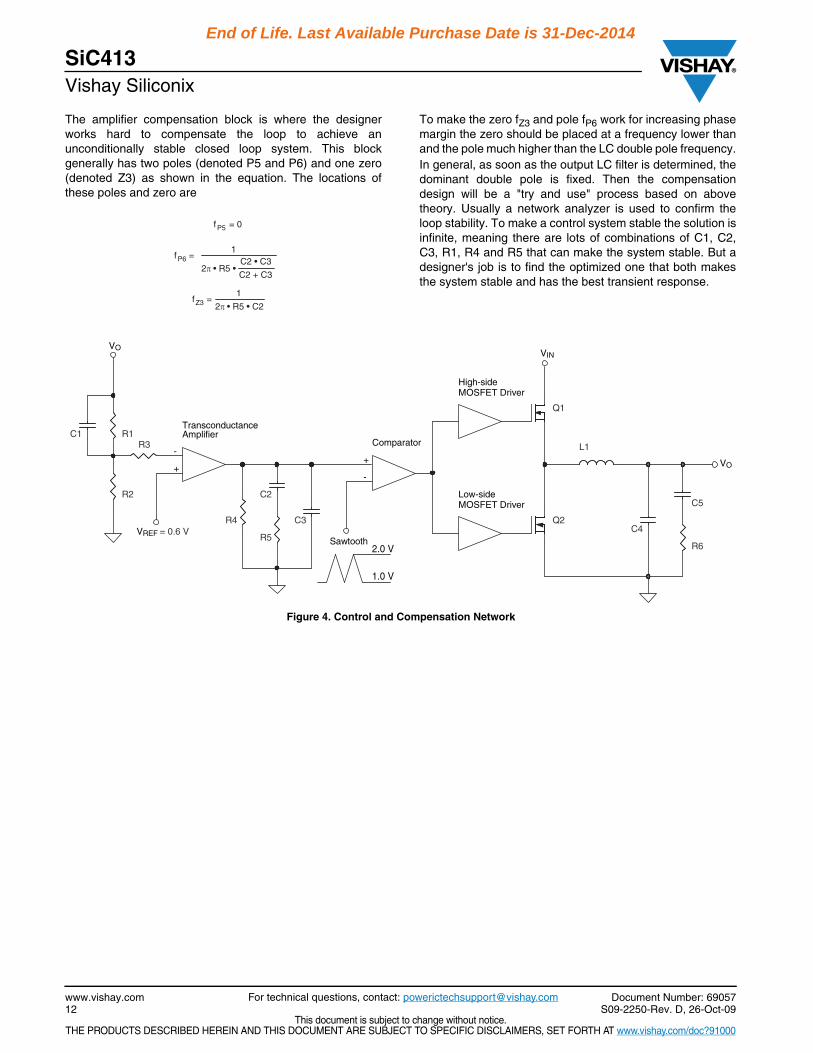
The amplifier compensation block is where the designerworks hard to compensate the loop to achieve anunconditionally stable closed loop system. This blockgenerally has two poles (denoted P5 and P6) and one zero(denoted Z3) as shown in the equation. The locations ofthese poles and zero are
To make the zero fZ3 and pole fP6 work for increasing phasemargin the zero should be placed at a frequency lower thanand the pole much higher than the LC double pole frequency.In general, as soon as the output LC filter is determined, thedominant double pole is fixed. Then the compensationdesign will be a "try and use" process based on abovetheory. Usually a network analyzer is used to confirm theloop stability. To make a control system stable the solution isinfinite, meaning there are lots of combinations of C1, C2,C3, R1, R4 and R5 that can make the system stable. But adesigner's job is to find the optimized one that both makesthe system stable and has the best transient response.
= 0P5f
2π • R5 •
1
C2 + C3
C2 • C3fP6 =
2π • R5 • C2
1fZ3 =
Figure 4. Control and Compensation Network
VO
VREF = 0.6 VSawtooth
VIN
VO
TransconductanceAmplifier
Comparator
+
-
-
+
High-sideMOSFET Driver
Low-sideMOSFET Driver
R3
R2C5
R1
Q2
Q1
C4C3
C2
L1C1
R5R6
R4
1.0 V
2.0 V
Vishay SiliconixSiC413
Document Number: 69057S09-2250-Rev. D, 26-Oct-09
www.vishay.com13
This document is subject to change without notice.THE PRODUCTS DESCRIBED HEREIN AND THIS DOCUMENT ARE SUBJECT TO SPECIFIC DISCLAIMERS, SET FORTH AT www.vishay.com/doc?91000
For technical questions, contact: [email protected]
End of Life. Last Available Purchase Date is 31-Dec-2014
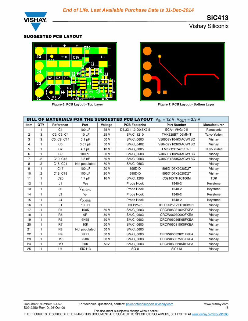
PCB LayoutAs in the design of any switching dc-to-dc converter, a goodPCB layout ensures successful transition from design toproduction. One of a few drawbacks of switching convertersis the noise generated by the high frequency switching andcoupled by parasitic inductance and capacitance. However,noise levels can be reduced or minimized if a PCB is well laidout.
The following is a guidance on SiC413 layout.Input Capacitors: C1 through to C6 are the input capacitors.They are placed side by side together to form a block and thisblock sits right beside SiC413's VIN and GND pins. Thisplacement minimizes the distance between VIN pin,capacitors and chip’s ground, which minimizes the possibilityof noise injected in VIN pin.Also the MLCC with smallest value (0.01 µF) is placedclosest to VIN pin, and then MLCC with larger values (0.1 µF,10 µF) and the last, the electrolytic. This is because theirESRs are getting larger and larger from small value MLCC tolarge value MLCC and then electrolytic capacitor.
Output Capacitors: C17 through to C20 are the outputcapacitors. They are placed the same way as inputcapacitors.
Decoupling Capacitors of VREG: C7 and C8, are placed rightbeside GND pin on their negative sides. Their positive sidesare connected to the chip's VREG pin through two vias fromthe bottom of the PCB. The trace distance should be keptless than 10 mm.
Boot Capacitor: C14 is the boot capacitor. R5 is added toallow flexibility for adjusting the high-side MOSFET drivingcurrent to reduce possible noise.
Compensation Network: C9, C10, R6 and R10 form thisnetwork. These components should be placed in a tightgroup. This group then should be in close proximity to theCOMP pin. Trace lengths between the components shouldbe minimized.
Output Sampling Network: R7, C15, R9 and R11 constitutethe output voltage sampling network. These componentsshould be placed in a tight grouping and in close proximity tothe FB pin. Since SiC413 has only one GND pin, this makesthe chip more sensitive to noise coming from GND.Therefore R11 is added to perform as a filter to remove anypossible noise from ground.
Grounding: Separate analog and power ground paths arerecommended for optimal noise reduction in the SiC413CBconverter. These grounds should both be connected at theGND pin. Connect the ground pin of the input and outputcapacitors to the power ground. Connect the ground pin forthe VREG decoupling caps, the compensation networkgrounds, and the output voltage sampling network groundsto the analog ground. It is preferred to use low inductanceground planes when ever possible. If single sided board isbeing used then try to keep the ground traces short andgoing a star configuration at the GND pin.
Power Traces: The power path is formed starting at VIN. Itthen branches to PGND and VSW to VOUT. The tracethickness for the power path should be kept to a minimum of50 mils. Placement of components should focus on keepingthese traces as short as possible to minimize parasiticinductance and resistances. They have minimum 50 miltrace width (at the VIN pin area) and this segment is veryshort, which is good enough for the power level handled bythis chip.Figure 6 and Figure 7 below show a recommended boardlayout for converters using SiC413CB.
Vishay SiliconixSiC413
www.vishay.com14
Document Number: 69057S09-2250-Rev. D, 26-Oct-09
This document is subject to change without notice.THE PRODUCTS DESCRIBED HEREIN AND THIS DOCUMENT ARE SUBJECT TO SPECIFIC DISCLAIMERS, SET FORTH AT www.vishay.com/doc?91000
For technical questions, contact: [email protected]
End of Life. Last Available Purchase Date is 31-Dec-2014
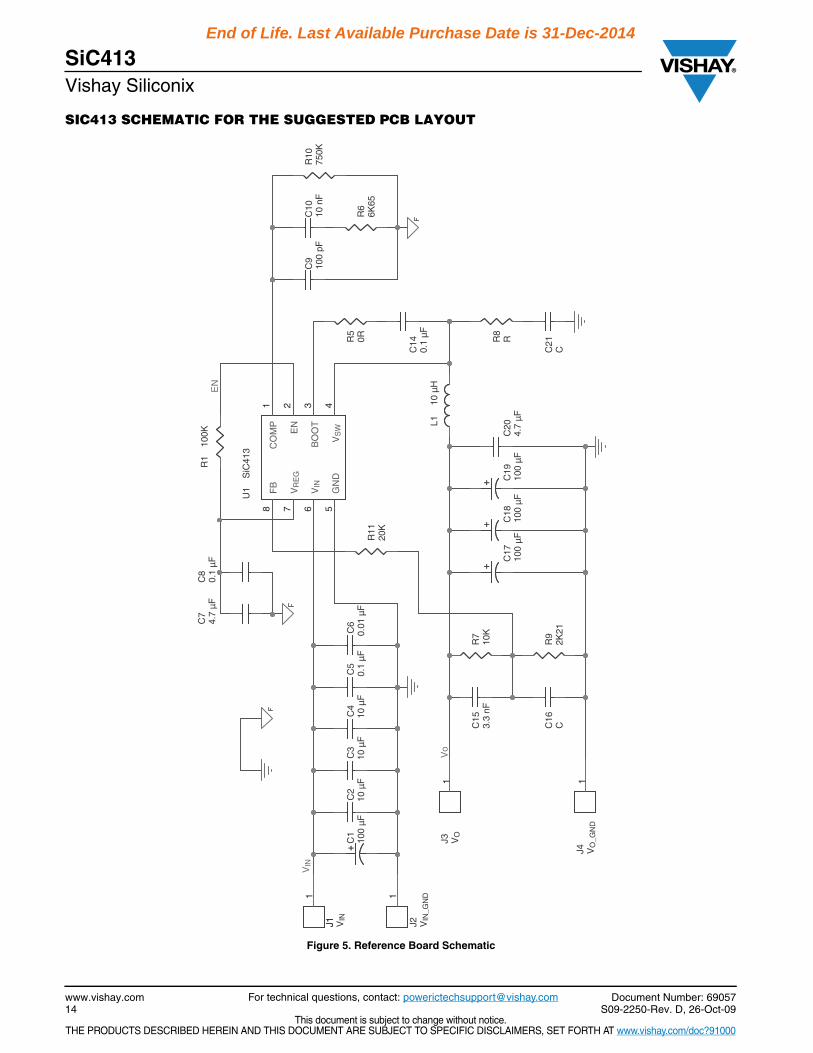
SIC413 SCHEMATIC FOR THE SUGGESTED PCB LAYOUT
Figure 5. Reference Board Schematic
Vo
EN
VIN
J4 VO
_GN
D1
C4
10 µ
FR
1120
K
C6
0.01
µF
C5
0.1
µF
J3 VO
1
C7
4.7
µF
J2 VIN
_GN
D1
R5
0R
J1 VIN
J1
1
+ C18
100
µF
+
C2
10 µ
FR
66K
65
U1
SiC
413 C
OM
P1
EN
2
BO
OT
3
VS
W4
FB
8
VR
EG
7
VIN
6
GN
D5
+ C19
100
µF
+R
8R
+
C17
100
µF
+
C8
0.1
µF
C14
0.1
µF
C20
4.7
µF
R10
750K
R9
2K21
C3
10 µ
F
C10
10 n
F
+C
110
0 µF
+
R7
10K
C9
100
pF
C21
C
R1
100K
C15
3.3
nF
L110
µH
C16
C
Vishay SiliconixSiC413
Document Number: 69057S09-2250-Rev. D, 26-Oct-09
www.vishay.com15
This document is subject to change without notice.THE PRODUCTS DESCRIBED HEREIN AND THIS DOCUMENT ARE SUBJECT TO SPECIFIC DISCLAIMERS, SET FORTH AT www.vishay.com/doc?91000
For technical questions, contact: [email protected]
End of Life. Last Available Purchase Date is 31-Dec-2014
SUGGESTED PCB LAYOUT
Figure 6. PCB Layout - Top Layer Figure 7. PCB Layout - Bottom Layer
BILL OF MATERIALS FOR THE SUGGESTED PCB LAYOUT VIN = 12 V, VOUT = 3.3 V Item QTY Reference Part Voltage PCB Footprint Part Number Manufacturer
1 1 C1 100 µF 35 V D6.3X11.2-D0.6X2.5 ECA-1VHG101I Panasonic
2 3 C2, C3, C4 10 µF 25 V SM/C_1210 TMK325B7106MN-T Taiyo Yuden
3 3 C5, C8, C14 0.1 µF 50 V SM/C_0603 VJ0603Y104KXACW1BC Vishay
4 1 C6 0.01 µF 50 V SM/C_0402 VJ0402Y103KXACW1BC Vishay
5 1 C7 4.7 µF 10 V SM/C_0805 LMK212B7475KG-T Taiyo Yuden
6 1 C9 100 pF 50 V SM/C_0603 VJ0603Y102KXACW1BC Vishay
7 2 C10, C15 3.3 nF 50 V SM/C_0603 VJ0603Y333KXACW1BC Vishay
8 2 C16, C21 Not populated 50 V SM/C_0603 Vishay
9 1 C17 100 µF 20 V 595D-D 595D107X9020D2T Vishay
10 2 C18, C19 100 µF 20 V 595D-D 595D107X9020D2T Vishay
11 1 C20 4.7 µF 16 V SM/C_1206 C3216X7R1C106M TDK
12 1 J1 VIN Probe Hook 1540-2 Keystone
13 1 J2 VIN_GND Probe Hook 1540-2 Keystone
14 1 J3 VO Probe Hook 1540-2 Keystone
15 1 J4 VO_GND Probe Hook 1540-2 Keystone
16 1 L1 10 µH IHLP2525 IHLP2525EZER100M01 Vishay
17 1 R1 100K 50 V SM/C_0603 CRCW0603100KFKEA Vishay
18 1 R5 0R 50 V SM/C_0603 CRCW06030000FKEA Vishay
19 1 R6 6K65 50 V SM/C_0603 CRCW06036K65FKEA Vishay
20 1 R7 10K 50 V SM/C_0603 CRCW060310K0FKEA Vishay
21 1 R8 Not populated 50 V SM/C_0603 Vishay
22 1 R9 2K21 50 V SM/C_0603 CRCW06032K21FKEA Vishay
23 1 R10 750K 50 V SM/C_0603 CRCW0603750KFKEA Vishay
24 1 R11 20K 50V SM/C_0603 CRCW060320K0FKEA Vishay
25 1 U1 SiC413 SO-8 SiC413 Vishay
Vishay SiliconixSiC413
www.vishay.com16
Document Number: 69057S09-2250-Rev. D, 26-Oct-09
This document is subject to change without notice.THE PRODUCTS DESCRIBED HEREIN AND THIS DOCUMENT ARE SUBJECT TO SPECIFIC DISCLAIMERS, SET FORTH AT www.vishay.com/doc?91000
For technical questions, contact: [email protected]
End of Life. Last Available Purchase Date is 31-Dec-2014
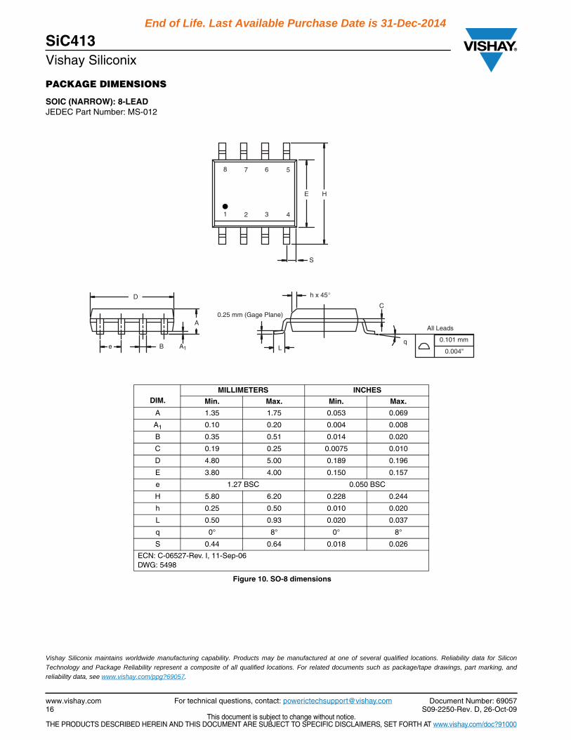
PACKAGE DIMENSIONS
SOIC (NARROW): 8-LEADJEDEC Part Number: MS-012
Vishay Siliconix maintains worldwide manufacturing capability. Products may be manufactured at one of several qualified locations. Reliability data for Silicon
Technology and Package Reliability represent a composite of all qualified locations. For related documents such as package/tape drawings, part marking, and
reliability data, see www.vishay.com/ppg?69057.
DIM.MILLIMETERS INCHES
Min. Max. Min. Max.
A 1.35 1.75 0.053 0.069
A1 0.10 0.20 0.004 0.008
B 0.35 0.51 0.014 0.020
C 0.19 0.25 0.0075 0.010
D 4.80 5.00 0.189 0.196
E 3.80 4.00 0.150 0.157
e 1.27 BSC 0.050 BSC
H 5.80 6.20 0.228 0.244
h 0.25 0.50 0.010 0.020
L 0.50 0.93 0.020 0.037
q 0° 8° 0° 8°
S 0.44 0.64 0.018 0.026
ECN: C-06527-Rev. I, 11-Sep-06DWG: 5498
Figure 10. SO-8 dimensions
4 3 1 2
5 6 8 7
H E
h x 45
C
All Leads
q 0.101 mm
0.004" L B A 1
A
e
D
0.25 mm (Gage Plane)
S
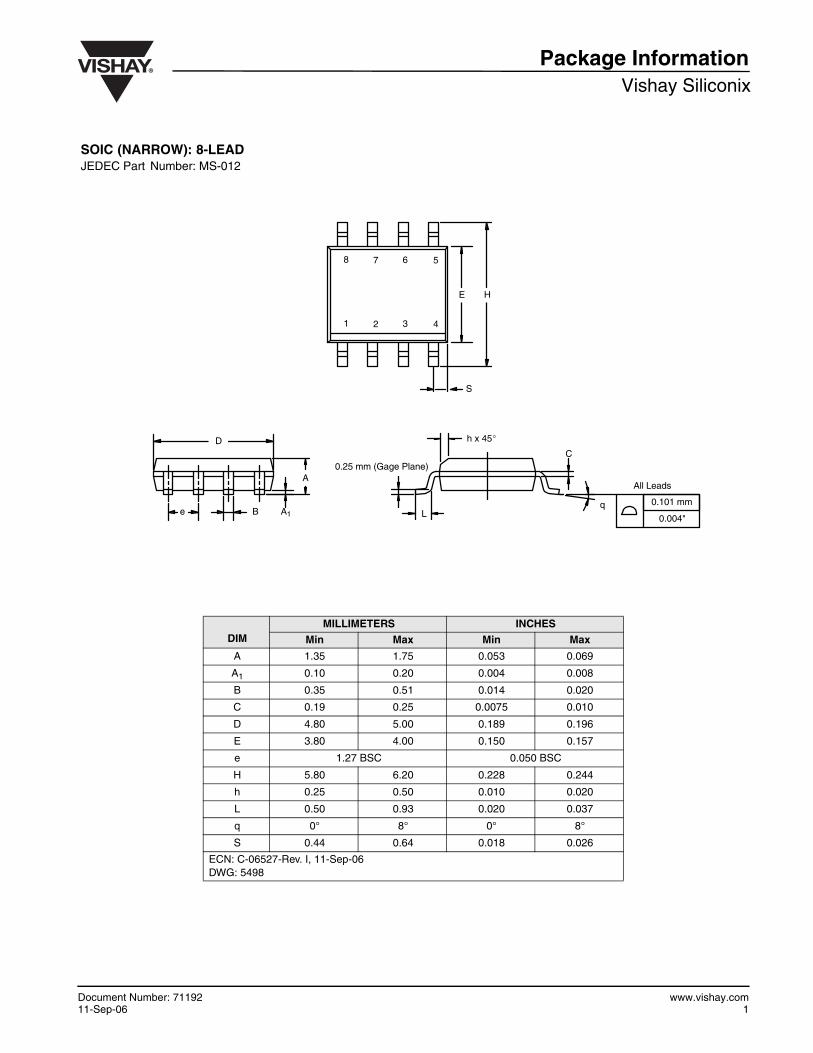
Vishay SiliconixPackage Information
Document Number: 7119211-Sep-06
www.vishay.com1
DIMMILLIMETERS INCHES
Min Max Min Max
A 1.35 1.75 0.053 0.069
A1 0.10 0.20 0.004 0.008
B 0.35 0.51 0.014 0.020
C 0.19 0.25 0.0075 0.010
D 4.80 5.00 0.189 0.196
E 3.80 4.00 0.150 0.157
e 1.27 BSC 0.050 BSC
H 5.80 6.20 0.228 0.244
h 0.25 0.50 0.010 0.020
L 0.50 0.93 0.020 0.037
q 0° 8° 0° 8°
S 0.44 0.64 0.018 0.026
ECN: C-06527-Rev. I, 11-Sep-06DWG: 5498
431 2
568 7
HE
h x 45
C
All Leads
q 0.101 mm
0.004"LB A1
A
e
D
0.25 mm (Gage Plane)
SOIC (NARROW): 8-LEADJEDEC Part Number: MS-012
S
Legal Disclaimer Noticewww.vishay.com Vishay
Revision: 08-Feb-17 1 Document Number: 91000
DisclaimerALL PRODUCT, PRODUCT SPECIFICATIONS AND DATA ARE SUBJECT TO CHANGE WITHOUT NOTICE TO IMPROVE RELIABILITY, FUNCTION OR DESIGN OR OTHERWISE.
Vishay Intertechnology, Inc., its affiliates, agents, and employees, and all persons acting on its or their behalf (collectively, “Vishay”), disclaim any and all liability for any errors, inaccuracies or incompleteness contained in any datasheet or in any other disclosure relating to any product.
Vishay makes no warranty, representation or guarantee regarding the suitability of the products for any particular purpose or the continuing production of any product. To the maximum extent permitted by applicable law, Vishay disclaims (i) any and all liability arising out of the application or use of any product, (ii) any and all liability, including without limitation special, consequential or incidental damages, and (iii) any and all implied warranties, including warranties of fitness for particular purpose, non-infringement and merchantability.
Statements regarding the suitability of products for certain types of applications are based on Vishay’s knowledge of typical requirements that are often placed on Vishay products in generic applications. Such statements are not binding statements about the suitability of products for a particular application. It is the customer’s responsibility to validate that a particular product with the properties described in the product specification is suitable for use in a particular application. Parameters provided in datasheets and / or specifications may vary in different applications and performance may vary over time. All operating parameters, including typical parameters, must be validated for each customer application by the customer’s technical experts. Product specifications do not expand or otherwise modify Vishay’s terms and conditions of purchase, including but not limited to the warranty expressed therein.
Except as expressly indicated in writing, Vishay products are not designed for use in medical, life-saving, or life-sustaining applications or for any other application in which the failure of the Vishay product could result in personal injury or death. Customers using or selling Vishay products not expressly indicated for use in such applications do so at their own risk. Please contact authorized Vishay personnel to obtain written terms and conditions regarding products designed for such applications.
No license, express or implied, by estoppel or otherwise, to any intellectual property rights is granted by this document or by any conduct of Vishay. Product names and markings noted herein may be trademarks of their respective owners.
© 2017 VISHAY INTERTECHNOLOGY, INC. ALL RIGHTS RESERVED