Embed Size (px)
Citation preview
SiC MESFET
Rajesh C. PandaEEL 6935
WBG ISpring 2003
Outline
• Introduction• Literature Review• Theory of MESFET Operation• Advantage of SiC MESFET• SiC Basic MESFET Structure• MESFET Specifications• SiC MESFET Application• Summary
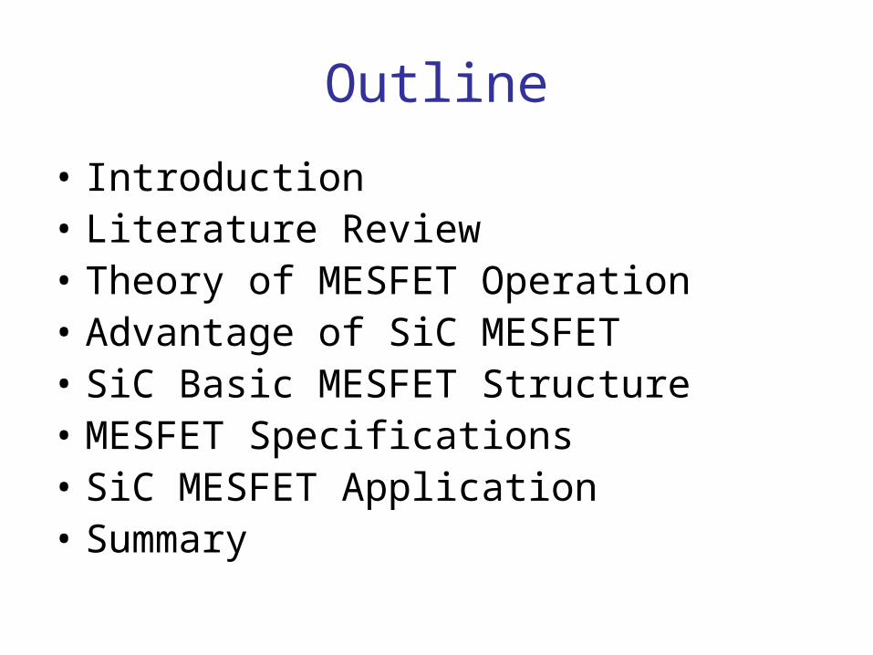
Literature Review• K. P. Hilton, M. J. Uren, D. G. Hayes, P. J. Wilding, H. K. Johnson, J. J. Guest and B. H. Smith,
"High power microwave SiC MESFET technology", in Workshop on High Performance Electron Devices for Microwave and Optoelectronic Applications, EDMO, 1999, pp. 71-74.
• S.T.Allen, J.W.Palmour, ,C.H.Carter,Jr., C.E.Weitzel, K.J.Nordquist, and L.L.Pond, III, “Silicon Carbide MESFET’s With 2 W/mm and 50% P.A.E. at 1.8 GHz ” IEEE MTT-S Symposium Digest, San Francisco, CA, June, 1996, pp. 681-684.
• ST Allen, RA Sadler, TS Alcorn, JW Palmour, CH Carter, "Silicon Carbide MESFET‘s for High Power S-Band Applications”, 1997, IEEE MTT-S Digest, pp. 57-60.
• SP Murray and KP Roenker, “An Analytical Model for SiC MESFETs,” Solid State Electr. vol. 46 (10), pp. 195-198, October 2002.
• KE Moore, CE Weitzel, Kevin J. Nordquist, Lauren L. Pond, III, John W. Palmour, Scott Allen, and Calvin H. Charter, Jr., “ 4H-SiC MESFET with 65.7 % power added efficiency at 850 MHz”, IEEE Electron Device Letters, Vol.18, No.2, February 1997.
• Inder Bahl and Prakash Bhartia, Microwave Solid State Circuit Design, A Wiley-Interscience Publication, 1988.
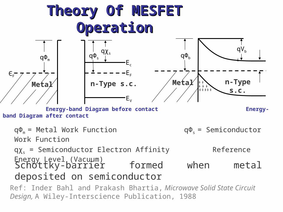
qΦs
qχs
Ec
EF
EV
qΦm
ЄF
Metal n-Type s.c.
qΦb
Metal n-Type s.c.
qVbi
Energy-band Diagram before contact Energy-band Diagram after contact
Theory Of MESFET OperationTheory Of MESFET OperationTheory Of MESFET OperationTheory Of MESFET Operation
qΦm = Metal Work Function qΦs = Semiconductor Work Function
qχs = Semiconductor Electron Affinity Reference Energy Level (Vacuum)
Schottky-barrier formed when metal deposited on semiconductor
Ref: Inder Bahl and Prakash Bhartia, Microwave Solid State Circuit Design, A Wiley-Interscience Publication, 1988
Theory Of MESFET OperationTheory Of MESFET OperationTheory Of MESFET OperationTheory Of MESFET Operation
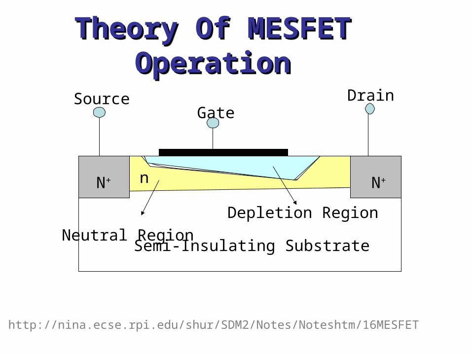
N+ N+
Semi-Insulating Substrate
Depletion Region
Neutral Region
GateSource Drain
n
Ref: http://nina.ecse.rpi.edu/shur/SDM2/Notes/Noteshtm/16MESFET

Theory Of MESFET OperationTheory Of MESFET Operation
S G D
DR
-
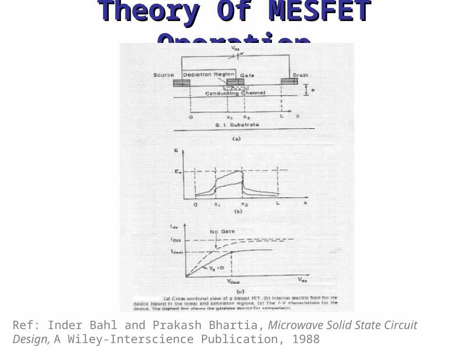
• VGS controls channel (DR)• VDS drifts carriers • Fully depleted channel = pinch off condition (Vpinch)
Depletion region forms under schottky contact (gate) and controls the flow of current in the channel (n-type) layer.
Device therefore behaves as voltage controlled switch, capable of very high speed modulation.
Ref: Inder Bahl and Prakash Bhartia, Microwave Solid State Circuit Design, A Wiley-Interscience Publication, 1988
Theory Of MESFET OperationTheory Of MESFET Operation
Ref: Inder Bahl and Prakash Bhartia, Microwave Solid State Circuit Design, A Wiley-Interscience Publication, 1988
Theory Of MESFET OperationTheory Of MESFET Operation
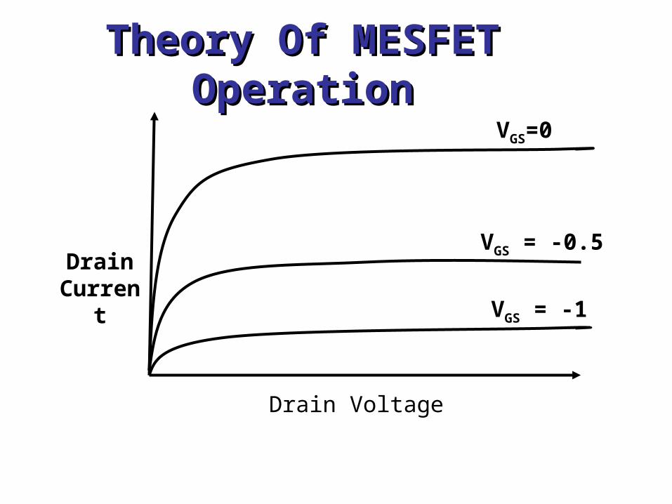
Drain Voltage
Drain Current
VGS = -1
VGS = -0.5
VGS=0
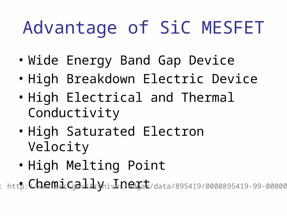
Advantage of SiC MESFET
• Wide Energy Band Gap Device
• High Breakdown Electric Device
• High Electrical and Thermal Conductivity
• High Saturated Electron Velocity
• High Melting Point
• Chemically Inert
Ref: http://www.sec.gov/Archives/edgar/data/895419/0000895419-99-000009.txt
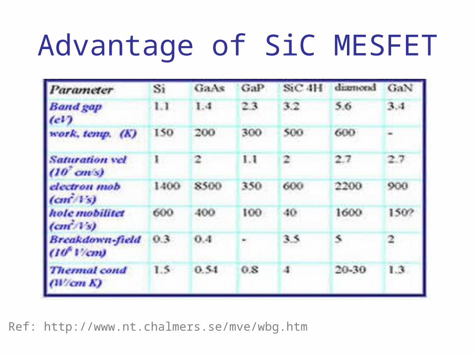
Advantage of SiC MESFET
Ref: http://www.nt.chalmers.se/mve/wbg.htm
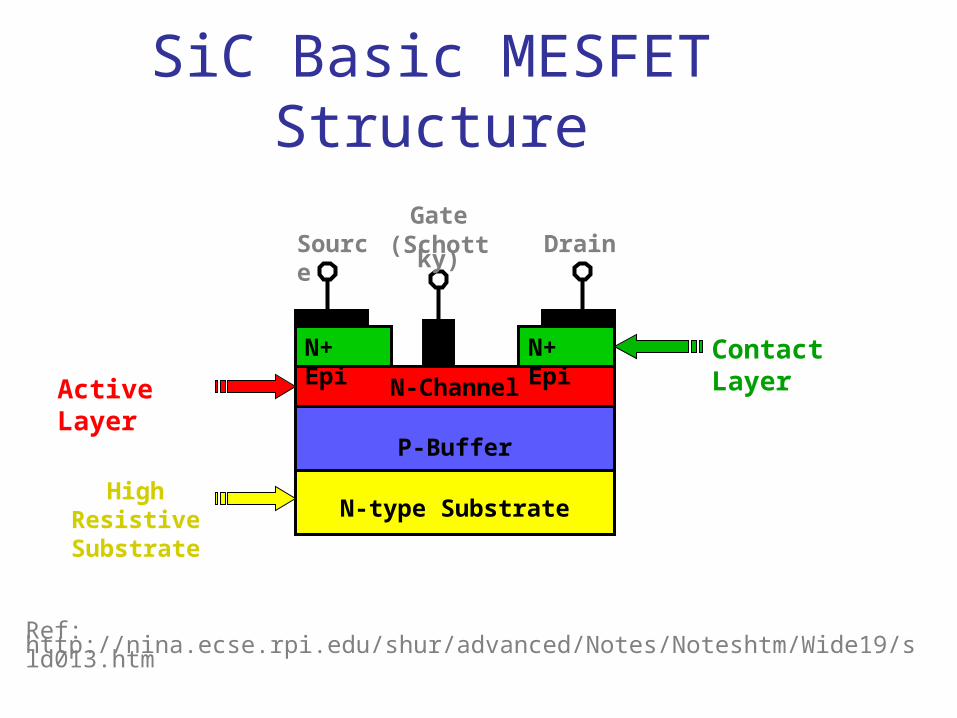
SiC Basic MESFET Structure
Source DrainGate
(Schottky)
N+ Epi N+ Epi
N-Channel
P-Buffer
N-type Substrate
Active Layer
High Resistive Substrate
Contact Layer
Ref: http://nina.ecse.rpi.edu/shur/advanced/Notes/Noteshtm/Wide19/sld013.htm
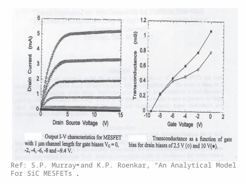
Ref: S.P. Murray and K.P. Roenkar, “An Analytical Model For SiC MESFETs”.
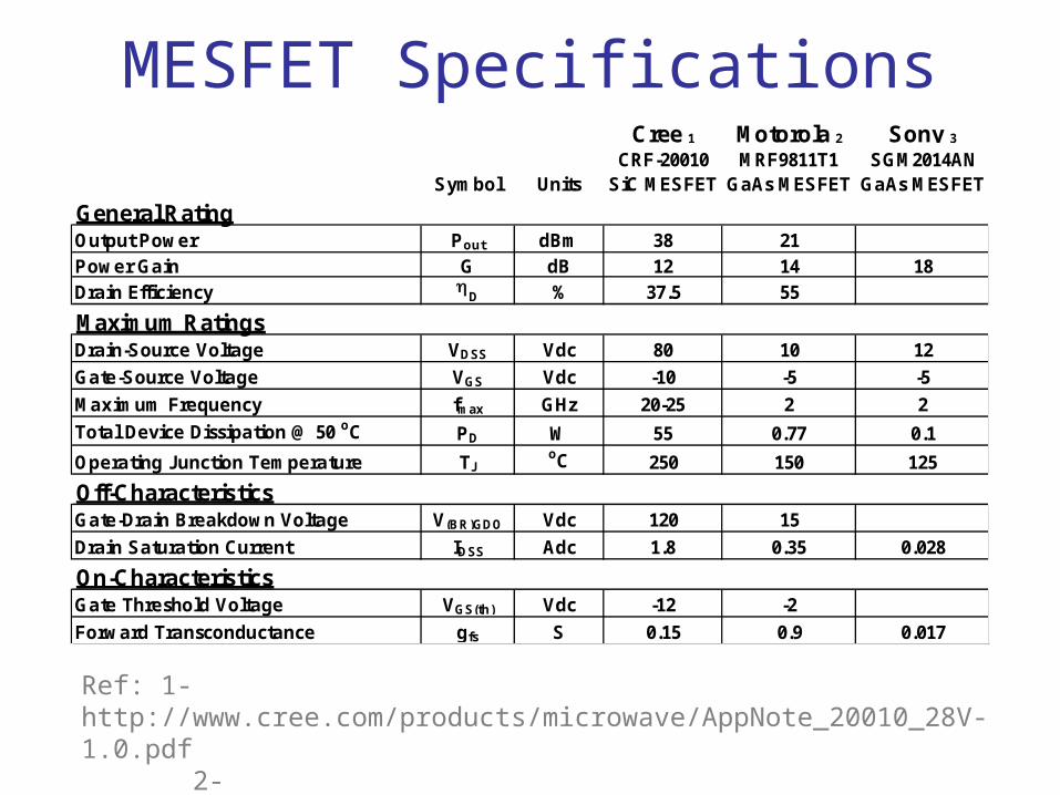
MESFET SpecificationsCree 1 Motorola 2 Sony 3
CRF-20010 MRF9811T1 SGM2014ANSymbol Units SiC MESFET GaAs MESFET GaAs MESFET
General RatingOutput Power Pout dBm 38 21Power Gain G dB 12 14 18Drain Efficiency h
D % 37.5 55
Maximum RatingsDrain-Source Voltage VDSS Vdc 80 10 12
Gate-Source Voltage VGS Vdc -10 -5 -5
Maximum Frequency fmax GHz 20-25 2 2
Total Device Dissipation @ 50 oC PD W 55 0.77 0.1
Operating Junction Temperature TJoC 250 150 125
Off-CharacteristicsGate-Drain Breakdown Voltage V(BR)GDO Vdc 120 15
Drain Saturation Current IDSS Adc 1.8 0.35 0.028
On-CharacteristicsGate Threshold Voltage VGS(th) Vdc -12 -2
Forward Transconductance gfs S 0.15 0.9 0.017
Ref: 1- http://www.cree.com/products/microwave/AppNote_20010_28V-1.0.pdf 2- http://www.mot-sps.com/books/dl110/pdf/mrf9811t1rev0d1.pdf 3- http://www.sel.sony.com/semi/PDF/SGM2014AN.pdf
MESFET Specifications
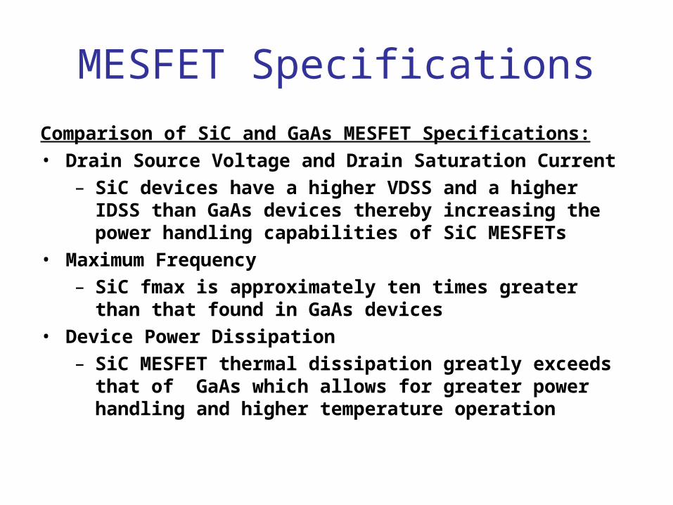
Comparison of SiC and GaAs MESFET Specifications:• Drain Source Voltage and Drain Saturation Current
– SiC devices have a higher VDSS and a higher IDSS than GaAs devices thereby increasing the power handling capabilities of SiC MESFETs
• Maximum Frequency– SiC fmax is approximately ten times greater than that found
in GaAs devices• Device Power Dissipation
– SiC MESFET thermal dissipation greatly exceeds that of GaAs which allows for greater power handling and higher temperature operation
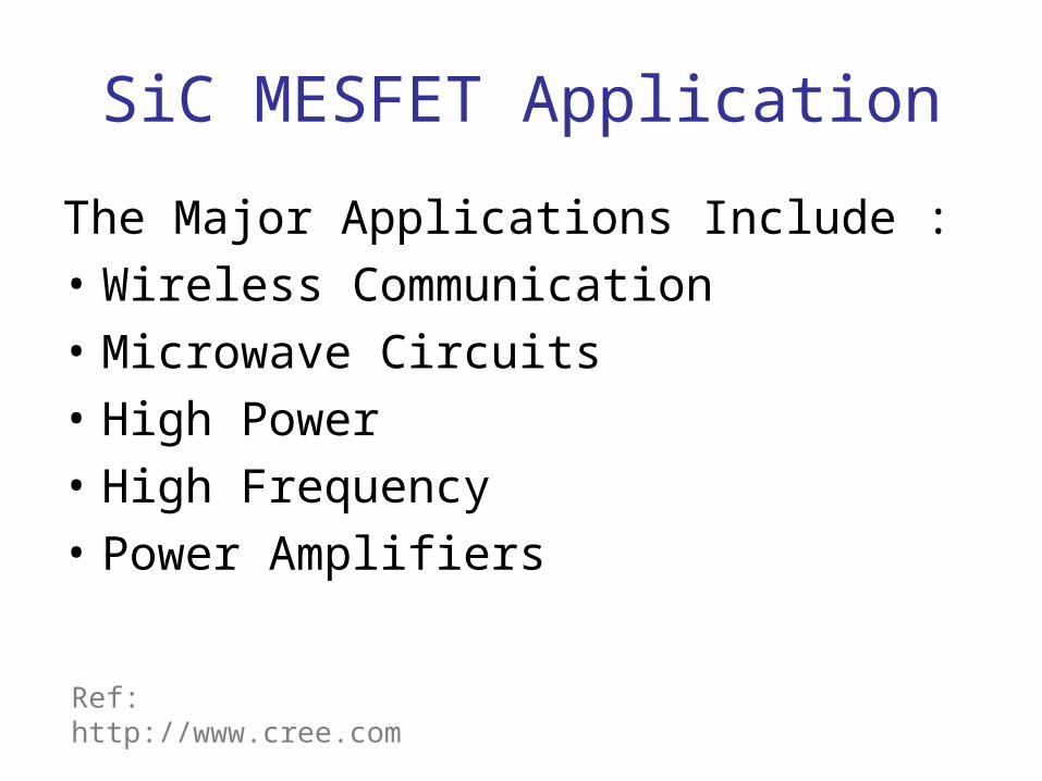
SiC MESFET Application
The Major Applications Include :
• Wireless Communication
• Microwave Circuits
• High Power
• High Frequency
• Power Amplifiers
Ref: http://www.cree.com
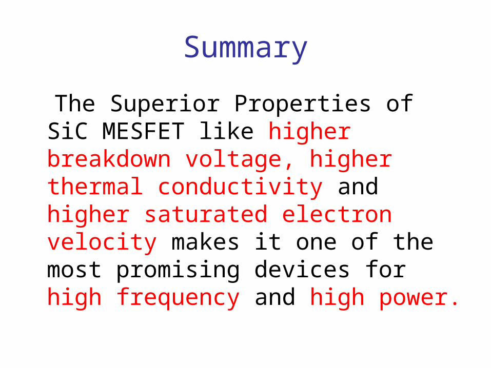
Summary
The Superior Properties of SiC MESFET like higher breakdown voltage, higher thermal conductivity and higher saturated electron velocity makes it one of the most promising devices for high frequency and high power.