Embed Size (px)
Citation preview

Si8751/52 Data Sheet
Isolated FET Driver with Pin Control or Diode Emulator InputsThe Si875x enables new pathways to the creation of custom Solid State Relay (SSR) con-figurations. The Si875x integrates robust isolation technology with an SSR FET driver. Afloating secondary side dc power supply is unnecessary as the product generates its ownself-contained gate drive output voltage. When combined with a customer-selected externalFET, a complete Solid State Relay is formed, allowing customers to optimize their systemfor cost, PCB area, power, On-Resistance, and thermal performance.
Customers have a choice of digital input control (Si8751) or diode emulation control(Si8752) to best suit their application. The Si875x integrates versatile outputs that supportdriving AC or DC load configurations.
The Si875x eliminates the need for bulky mechanical relays which can be difficult to assem-ble onto PCBs and add switching noise to the system.
Traditional SSRs integrate optocoupler-style LED inputs, which limit the operating tempera-ture range of the solution. The Si875x experiences no such limitation and can support fullindustrial and automotive temperature ranges with increased stability and longer life.
The Si875x drives FET gates with a nominal 10 V using as little as 1 mA input current. In-creasing the input current to 10 mA enables turn-on times as fast as 94 μs. Input side vol-tages on the Si8751 are flexible from 2.25 V to 5.5 V supporting seamless connection tolow-power controllers. The Si875x devices provide an Active Miller Clamp to prevent the un-intended turn-on of the external FET when a high dV/dt is present on the FET’s drain.
The Si875x is qualified to the AEC-Q100 standard, making it suitable for automotive applica-tions. Further, its 2.5 KVrms isolation rating forms the basis for full certification to UL, CSA,VDE, and CQC.
Applications include mechanical relay, photo switch, or SSR replacement in motor control,valve control, HVAC relay, automotive, charging, battery monitoring, ac mains line switch-ing, and more.The Si8751 and Si8752 come in ROHS-compliant SOIC-8 packaging, providing a compact,industry-standard footprint and generous margin to creepage and clearance requirements.
KEY FEATURES
• Drives user-selected external FETs• Choice of digital input control (Si8751)
or diode emulation control (Si8752)• Internally generated secondary side
power supply• 10 V output with 1 mA input current• As fast as 82 μs turn-on time and 46
us turn-off time• Active Miller Clamp to prevent
unintended turn-on and reduceinductive chatter
• Supports AC or DC load switching• 2.5 KVrms isolation rating• UL, CSA, VDE, and CQC certifications• AEC-Q100 qualified• Industrial –40 to 105 °C or Automotive
–40 to 125 °C temperature ranges• ROHS-compliant SOIC-8 Package
APPLICATIONS
• Motor Controls• Valve Controls• HVAC Relays• HEV/EV Automotive Charging• Battery Monitoring• AC Mains Line Switching
silabs.com | Building a more connected world. Rev. 1.0

1. Ordering Guide
Table 1.1. Si8751/2 Ordering Guide
Ordering Part Number1,2
Input Support Package Temperature Range (Ambient) Isolation Rating (kVrms)
Si8751AB-IS Digital CMOS SOIC-8 –40 to 105 °C Industrial 2.5 kV
Si8751AB-AS Digital CMOS SOIC-8 –40 to 125 °C Automotive 2.5 kV
Si8752AB-IS Diode Emulation SOIC-8 –40 to 105 °C Industrial 2.5 kV
Si8752AB-AS Diode Emulation SOIC-8 –40 to 125 °C Automotive 2.5 kV
Note:1. "Si" and "SI" are used interchangeably.2. Add an “R” at the end of the device to denote tape and reel option
Si8751/52 Data SheetOrdering Guide
silabs.com | Building a more connected world. Rev. 1.0 | 2

2. System Overview
Sign
al &
Pow
er T
rans
mitt
er
CMO
S Is
olat
ion
MCAP1
GATE
SOURCE
IN
VDD
TT
GNDMCAP2
Rece
iver
Figure 2.1. Si8751 Block Diagram
CMO
S Is
olat
ion
MCAP1
GATE
SOURCE
MCAP2
ANODE
CATHODE
e
Sign
al &
Pow
er T
rans
mitt
er
Rece
iver
Figure 2.2. Si8752 Block Diagram
Si8751/52 Data SheetSystem Overview
silabs.com | Building a more connected world. Rev. 1.0 | 3
The operation of an Si875x channel is analogous to that of an optocoupler and gate driver, except an RF carrier is modulated instead oflight. This simple architecture provides a robust isolated data path and requires no special considerations or initialization at start-up. Asimplified block diagram for a single Si875x channel is shown in the figure below.
MODULATOR DEMODULATOR
RF OSCILLATOR
Semiconductor-Based Isolation
Barrier
Transmitter Receiver
A B
Figure 2.3. Simplified Channel Diagram
A channel consists of an RF Transmitter and RF Receiver separated by a semiconductor-based isolation barrier. Referring to theTransmitter, input A modulates the carrier provided by an RF oscillator using on/off keying. The Receiver contains a demodulator thatdecodes the input state according to its RF energy content and applies the result to output B via the output driver. This RF on/off keyingscheme is superior to pulse code schemes as it provides best-in-class noise immunity, low power consumption, and better immunity tomagnetic fields. See figure below for more details.
Input Signal
Output Signal
Modulation Signal
Figure 2.4. Modulation Scheme
2.1 Device Behavior
The following are truth tables for the Si875x family.
Table 2.1. Si8751 Truth Table
VDD IN Gate
Powered H H
Powered L L
Unpowered X L
Table 2.2. Si8752 Truth Table
Input Current Gate
> If(TH) H
< If(TH) L
Si8751/52 Data SheetSystem Overview
silabs.com | Building a more connected world. Rev. 1.0 | 4

2.2 Power Supply Connections (Si8751 Only)
The Si8751 requires a 0.1 µF bypass capacitor between VDD and GND. The capacitor should be placed as close as possible to thepackage. To enhance the robustness of a design, the user may also include a 1 µf capacitor for bulk decoupling as well as a resistor(50–300 Ω) in series with the input if the system is excessively noisy.
2.3 TT Pin Description (Si8751 Only)
The Si8751 provides a pin to control how much current is consumed by the supply when the input pin is logic high. The more currentconsumed by the input supply, the faster the output can turn on the external FET. This allows the application designer to optimize thetradeoff between power consumption and switching time.
Typically, this pin is connected to the supply ground through a resistor. The greater the value of the resistor, the less current is con-sumed by the input supply. Values can range from 0 Ω (shorted to ground) to open (TT not connected).
In addition to a resistor, a capacitor, typically 0.1 µf, can be placed in parallel to the resistor. This allows the device to draw more currentto switch the external FET on quickly yet draw less supply current in the steady state. Total power over time is reduced while maintain-ing fast switching of the FET.
TT
IN
Sign
al &
Pow
er T
rans
mitt
er
CMO
S Is
olat
ion
MCAP1
GATE
SOURCE
IN
VDD
GND
Rece
iver
MCAP2
Figure 2.5. Si8751 TT Example
Max DriveCurrent
Static DriveCurrent
~1/C
t
Figure 2.6. Drive Current vs. Time Using TT with Capacitor
2.4 LED Emulator Input (Si8752 Only)
Figure 2.8. Diode Emulator Model and I-V Curve
The Si8752 uses input current to achieve the development of power across the isolation barrier. Therefore, the more current provided tothe input, the more power is developed on the isolated side of the device. This translates into a faster turn on time of the external FET.This benefit is limited to an input current of about 15 mA. Beyond that, increasing the input current has little effect on the switching timeof the external FET.
Si8751/52 Data SheetSystem Overview
silabs.com | Building a more connected world. Rev. 1.0 | 5

2.5 Output Description
The output of the Si875x device develops a positive voltage on the GATE pin with respect to the SOURCE pin. This voltage is used toturn on a typical field effect transistor (FET). Because power is transmitted across the isolation barrier, no isolated supply is required.
This can be used to drive a FET configured as a switch for a dc load. It can also be used to drive a pair of FETs configured as a switchfor an ac load. See 3. Applications.
2.6 Miller Clamp
2.6.1 Miller Clamp Description
The Si875x devices provide a clamping device to prevent unintended turn on of the external FET when a high dV/dt is present on theFET’s drain. To use this feature, a capacitor is connected between the drain(s) of the FET(s) and one of the MCAPx inputs. A sudden,positive slope on this pin will cause the clamp device within the Si875x to activate and provide a low impedance path between the gateand source pins. This will prevent the FET from being unintentionally turned on.
The Si875x device provides two miller clamp input pins. This allows for both FET’s to be protected from unintended turn on when thedevice is used in an AC switch configuration. In this case each drain is connected to an MCAPx input through a capacitor.
Connection to a MCAPx pin, and use of the Miller Clamp feature, is optional. The device will function as expected if these pins are leftunconnected.
2.6.2 Sizing Miller Clamp Capacitors
The recommended value of the capacitor used to connect the drain of the external FET to the Si875x device is typically 10 pf. If theapplication has a very large dV/dt and the clamp is not adequately keeping the external FET off, then this capacitor value can be in-creased up to 100 pf. The voltage rating of the capacitor should be greater than or equal to the peak voltage expected at the drain ofthe FET. The relationship of the capacitor and the dV/dt is governed by the equation: C = IMC/(dV/dt); where: IMC is the Miller Clampinput current (6mA max, as specified in Electrical Tables), and dV/dt is the expected slew rate.
Si8751/52 Data SheetSystem Overview
silabs.com | Building a more connected world. Rev. 1.0 | 6

3. Applications
The following examples illustrate typical circuit configurations using the Si8751/52.
3.1 DC SSR Example
The Si875x device can be used to control a dc load as shown in the following figure:
Sign
al &
Pow
er T
rans
mitt
er
CMO
S Is
olat
ion
MCAP1
GATE
SOURCE
IN
MCAP2
VDD
TT
GND
VDC
DC LoadRe
ceiv
er
Figure 3.1. Driving an FET for DC Load Including Miller Clamp Capacitor
In this configuration, the Si8751 charges the gate of the external FET; turning it on. This switches on power, supplied by VDC, to theload. The output side circuitry is identical if using the Si8752.
3.2 AC SSR Example
The Si875x can be used to control power to an ac load using the following circuit:
AC Load
ACSupply
Sign
al &
Pow
er T
rans
mitt
er
CMO
S Is
olat
ion
MCAP1
GATE
SOURCE
IN
VDD
TT
GND
Rece
iver
MCAP2
Figure 3.2. Driving FETs for AC Load Switching
In this configuration, both FET’s are turned on by the charge delivered by the Si8751. This allows ac current to flow to the load. Whenthe Si875x is turned off, charge is drained form the gates of both FET’s and the ac current is turned off. The output side circuitry isidentical if using the Si8752.
Si8751/52 Data SheetApplications
silabs.com | Building a more connected world. Rev. 1.0 | 7

4. Electrical Specifications
Table 4.1. Electrical Specifications
• Automotive: VDD=2.25 to 5.5V; GND=0V; TA=-40 to +125ºC; typical specs at 25ºC; TJ=-40 to +150ºC• Industrial: VDD=2.25 to 5.5V; GND=0V; TA=-40 to +105ºC; typical specs at 25ºC; TJ=-40 to +150ºC
Parameter Symbol Test Condition Min Typ Max Unit
Si8751 Only
Input Side
Supply Voltage VDD 2.25 3.3 5.5 V
Supply Current IDD IN = 0V — 140 — nA
IN = VDD, TT = GND — 13.8 17 mA
IN = VDD, TT = 10 kΩ — 7.8 9.5 mA
IN = VDD, TT unconnected — 1.5 1.8 mA
High Level Input Voltage VIH 50% of VDD — — V
Low Level Input Voltage VIL — — 25% of VDD V
Input Hystersis VHYS — 180 — mV
Driver Side
GATE Off Voltage VG(OFF) IN = 0 V — 0 — mV
GATE On Voltage VG(ON) IN = VDD, TT = GND 7.5 10 13 V
IN = VDD, TT = 10 kΩ 9 10.8 13 V
IN = VDD, TT unconnected 9 10.8 13 V
GATE On Impedance RG IN = VDD, TT = GND — 162 330 kΩ
IN = VDD, TT = 10 kΩ — 265 370 kΩ
IN = VDD, TT unconnected — 1.5 1.85 MΩ
Turn-off Time TG(OFF) IN = 0 V — 15 35 µs
Turn-on Time (50% of VG(ON)) TG(ON) TT = GND — 42 120 µs
TT = 10 kΩ — 58 170 µs
TT unconnected — 286 650 µs
Turn-on Time (90% of VG(ON)) TG(ON) TT = GND — 85.3 190 µs
TT = 10 kΩ — 130 260 µs
TT unconnected — 0.7 1.2 ms
Si8752 Only
Input Side
Input Current IF(ON) 1.0 — 30.0 mA
Guaranteed Off Current IF(OFF) — — 10 µA
Forward Voltage (OFF) VF(OFF) Measured ANODE with respect to Cathode — 0 — V
Si8751/52 Data SheetElectrical Specifications
silabs.com | Building a more connected world. Rev. 1.0 | 8

Parameter Symbol Test Condition Min Typ Max Unit
Forward Voltage (ON) VF(ON) 1 mA < IF < 10 mA, measured ANODE with re-spect to cathode
1.8 — 2.35 V
10 mA < IF < 30 mA, measured ANODE withrespect to cathode
2.03 — 2.7 V
Driver Side
GATE Off Voltage VG(OFF) IF = 0 mA — 0 — mV
GATE On Voltage VG(ON) IF = 1 mA 8 10.3 13 V
IF = 10 mA 8 10.3 13 V
IF = 30 mA 8 10.9 13 V
GATE On Impedance RG IF = 1 mA — 2.7 3.5 MΩ
IF = 10 mA — 194 300 kΩ
IF = 30 mA — 168 290 kΩ
Turn-off Time TG(OFF) IF = 0 mA — 15 35 µs
Turn-on Time (50% of VG(ON)) TG(ON) IF = 1 mA — 463 720 µs
IF = 10 mA — 41 125 µs
IF = 30 mA — 36 90 µs
Turn-on Time (90% of VG(ON)) TG(ON) IF = 1 mA — 1.1 1.49 ms
IF = 10 mA — 94 190 µs
IF = 30 mA — 82 180 µs
Si8751 and Si8752
Miller Clamp Current IMC Max input current — — 6 mA
Miller Clamp Pull-Down Current IG IMC = 50 µA; VGate = 1 V 5 12.8 — mA
Gate OFF Impedance IF = 0 mA (Si8752)
IN = 0 V (Si8751)
— 21.5 — MΩ
Common Mode Transient Immunity VCM = 1500 V 20 — — kV/µs
Note:1. All measurements use 100 pF gate capacitance load unless specified.
Si8751/52 Data SheetElectrical Specifications
silabs.com | Building a more connected world. Rev. 1.0 | 9

4.1 Test Circuits
The following figure depicts a common-mode transient immunity test circuit:
Oscilloscope
High-Voltage Differential
Probe
Si8751VDD
TTIN
GND
MCAP1
SOURCE
GATE
MCAP2+-
IsolatedSupply
IsolatedGround
High-Voltage Surge Generator
Figure 4.1. Common-Mode Transient Immunity Test Circuit
4.2 Regulatory Information
Table 4.2. Regulatory Information1,2
CSA
The Si875x is certified under CSA Component Acceptance Notice 5A. For more details, see Master Contract Number 232873.
60950-1: Up to 125 VRMS reinforced insulation working voltage; up to 600 VRMS basic insulation working voltage.
VDE
The Si875x is certified according to VDE 0884-10. For more details, see Certificate 40018443.
VDE 0884-10: Up to 630 Vpeak for basic insulation working voltage.
UL
The Si875x is certified under UL1577 component recognition program. For more details, see File E257455.
Rated up to 2500 VRMS isolation voltage for basic protection.
CQC
The Si875x is certified under GB4943.1-2011. For more details, see Certificate CQC17001177960.
Rated up to 125 VRMS reinforced insulation working voltage; up to 600 VRMS basic insulation working voltage.
1. Regulatory Certifications apply to 2.5 kVRMS rated devices which are production tested to 3.0 kVRMS for 1 sec.2. For more information, see 1. Ordering Guide.
Si8751/52 Data SheetElectrical Specifications
silabs.com | Building a more connected world. Rev. 1.0 | 10

Table 4.3. Insulation and Safety-Related Specifications
Parameter Symbol Test Condition SOIC-8 Value Unit
Nominal External Air Gap
(Clearance)
CLR 4.7 mm
Nominal External Tracking
(Creepage)
CPG 3.9 mm
Minimum Internal Gap
(Internal Clearance)
DTI 0.008 mm
Tracking Resistance PTI IEC60112 600 V
Erosion Depth ED 0.04 mm
Resistance
(Input-Output)1
RIO 1012 Ω
Capacitance
(Input-Output)1
CIO f = 1 MHz 0.5 pF
Input Capacitance2 CI 3.0 pF
Notes:1. To determine resistance and capacitance, the Si875x is converted into a 2-terminal device. All pins on side 1 are shorted to cre-
ate terminal 1, and all pins on side 2 are shorted to create terminal 2. The parameters are then measured between these twoterminals.
2. Measured from input pin to ground.
Table 4.4. IEC 60664-1 Ratings
Parameter Test Condition SOIC-8 Specification
Basic Isolation Group Material Group I
Installation Classification Rated Mains Voltages < 150 VRMS I-IV
Rated Mains Voltages < 300 VRMS I-III
Rated Mains Voltages < 400 VRMS I-II
Rated Mains Voltages < 600 VRMS I-II
Si8751/52 Data SheetElectrical Specifications
silabs.com | Building a more connected world. Rev. 1.0 | 11

Table 4.5. VDE 0884 Insulation Characteristics1
Parameter Symbol Test Condition Characteristic Unit
Maximum Working Insulation Voltage VIORM 630 V peak
Input to Output Test Voltage VPR Method b1(VIORM x 1.875 = VPR, 100%Production Test, tm = 1 sec,Partial Discharge < 5 pC)
1181 V peak
Transient Overvoltage VIOTM t = 60 sec 4000 V peak
Surge Voltage VIOSM Tested per IEC 60065 with surgevoltage of 1.2 µs/50 µs
Si875x tested with 4000 V
3077Vpeak
Pollution Degree
(DIN VDE 0110, Table 1)
2
Insulation Resistance at
TS, VIO = 500 V
RS >109 Ω
Note:1. Maintenance of the safety data is ensured by protective circuits. The Si875x provides a climate classification of 40/125/21.
Table 4.6. IEC Safety Limiting Values1
Parameter Symbol Test Condition SOIC-8 Unit
Safety Temperature TS 150 °C
Safety Input Current(Si8751)
ΙS θJA = 110 °C/W
VDD = 5.5 V,
TJ = 150 °C,
TA = 25 °C
206 mA
θJA = 110 °C/W
VDD = 3.63 V,
TJ = 150 °C,
TA = 25 °C
313 mA
θJA = 110 °C/W
VDD = 2.75 V,
TJ = 150 °C,
TA = 25 °C
413 mA
Safety Input Current(Si8752)
ΙS θJA = 110 °C/W
VF = 2.5 V,
TJ = 150 °C,
TA = 25 °C
454 mA
Si8751/52 Data SheetElectrical Specifications
silabs.com | Building a more connected world. Rev. 1.0 | 12
Parameter Symbol Test Condition SOIC-8 Unit
Safety Input Power(Si8752)
PS θJA = 110 °C/W
VF = 2.5 V,
TJ = 150 °C,
TA = 25 °C
1136 mW
Device Power Dissipation PD 1 W
Note:1. Maximum value allowed in the event of a failure. Refer to the thermal derating curves below.
Si8751/52 Data SheetElectrical Specifications
silabs.com | Building a more connected world. Rev. 1.0 | 13

Table 4.7. Thermal Characteristics
Parameter Symbol SOIC-8 Unit
IC Junction-to-Air Thermal Resistance
θJA 110 °C/W
Figure 4.2. Thermal Derating Curve for Safety Limiting Current (Si8751)
Figure 4.3. Thermal Derating Curve for Safety Limiting Current (Si8752)
Si8751/52 Data SheetElectrical Specifications
silabs.com | Building a more connected world. Rev. 1.0 | 14

Table 4.8. Absolute Maximum Ratings1
Parameter Symbol Min Max Units
Storage Temperature TSTG –65 +150 °C
Operating Temperature TA –40 +125 °C
Junction Temperature TJ — +150 °C
Input-side supply voltage (Si8751) VDD –0.6 6.0 V
Voltage on any input side pin with respect to ground (pin4, Si8751 only)
VIO –0.5 VDD + 0.5 V
Average Forward Anode Current (Si8752) IF(AVG) — 30 mA
Reverse Anode Voltage (Si8752) VR — 0.3 V
Lead Solder Temperature (10 s) — 260 °C
ESD Rating, HBM — 3500 V
ESD Rating, CDM — 2000 V
Maximum Isolation Voltage (Input to Output) (1 sec)
SOIC-8
— 3000 VRMS
Latch-up Immunity — 400 kV/μs
Note:1. Permanent device damage may occur if the absolute maximum ratings are exceeded. Functional operation should be restricted to
the conditions specified in the operational sections of this data sheet.
Si8751/52 Data SheetElectrical Specifications
silabs.com | Building a more connected world. Rev. 1.0 | 15

4.3 Typical Operating Characteristics
Figure 4.4. Si8751 Typical Gate Voltage vs. Temperatureand TT
Figure 4.5. Si8752 Typical Gate Voltage vs. Temperatureand Anode Current
Figure 4.6. Si8751 Typical Turn-On Time vs. Temperatureand TT with 100 pF Load (50% of Output)
Figure 4.7. Si8752 Typical Turn-On Time vs. Temperatureand Anode Current with 100 pF Load (50% of Output)
Si8751/52 Data SheetElectrical Specifications
silabs.com | Building a more connected world. Rev. 1.0 | 16

Figure 4.8. Si8751 Typical Turn-On Time vs. Temperatureand TT with 100 pF Load (90% of Output)
Figure 4.9. Si8752 Typical Turn-On Time vs. Temperatureand Anode Current with 100 pF Load (90% of Output)
Figure 4.10. Si8751 Typical Turn-On Time vs. Capacitanceand TT (50% of Output)
Figure 4.11. Si8752 Typical Turn-On Time vs. Capacitanceand Anode Current (50% of Output)
Si8751/52 Data SheetElectrical Specifications
silabs.com | Building a more connected world. Rev. 1.0 | 17

Figure 4.12. Si8751 Typical Turn-On Time vs. Capacitanceand TT (90% of Output)
Figure 4.13. Si8752 Typical Turn-On Time vs. Capacitanceand Anode Current (90% of Output)
Si8751/52 Data SheetElectrical Specifications
silabs.com | Building a more connected world. Rev. 1.0 | 18

5. Pin Descriptions
5.1 Si8751 Pin Descriptions
1
2
3
4 5
6
7
8
SOURCE
MCAP2
MCAP1
GATE
GND
TT
VDD
Si8751IN
Figure 5.1. Pin Assignments Si8751
Table 5.1. Si8751 Pin Descriptions
Pin Name Description
1 VDD Input side power supply
2 TT Turn-on time control (optional)
3 IN Digital control input
4 GND Input side ground
5 SOURCE Connection to switch FET Source
6 MCAP2 Miller capacitance control 2 (optional)
7 MCAP1 Miller capacitance control 1 (optional)
8 GATE Connection to switch FET Gate
Si8751/52 Data SheetPin Descriptions
silabs.com | Building a more connected world. Rev. 1.0 | 19

5.2 Si8752 Pin Descriptions
1
2
3
4 5
6
7
8 GATE
MCAP2
MCAP1
SOURCECATHODE
ANODE
NC
Si8752NC
Figure 5.2. Pin Assignments Si8752
Table 5.2. Si8752 Pin Descriptions
Pin Name Description
1 NC No Connect
2 ANODE Anode of LED emulator
3 NC No Connect
4 CATHODE Cathode of LED emulator
5 SOURCE Connection to switch FET Source
6 MCAP2 Miller capacitance control 2 (optional)
7 MCAP1 Miller capacitance control 1 (optional)
8 GATE Connection to switch FET Gate
Si8751/52 Data SheetPin Descriptions
silabs.com | Building a more connected world. Rev. 1.0 | 20

6. Package Outlines
6.1 Package Outline: 8-Pin Narrow Body SOIC
The figure below illustrates the package details for the Si875x in an 8-pin narrow-body SOIC package. The table below lists the valuesfor the dimensions shown in the illustration.
Figure 6.1. 8-Pin Narrow Body SOIC Package
Si8751/52 Data SheetPackage Outlines
silabs.com | Building a more connected world. Rev. 1.0 | 21

Table 6.1. 8-Pin Narrow Body SOIC Package Diagram Dimensions
Symbol Millimeters
Min Max
A 1.35 1.75
A1 0.10 0.25
A2 1.40 REF 1.55 REF
B 0.33 0.51
C 0.19 0.25
D 4.80 5.00
E 3.80 4.00
e 1.27 BSC
H 5.80 6.20
h 0.25 0.50
L 0.40 1.27
α 0° 8°
Si8751/52 Data SheetPackage Outlines
silabs.com | Building a more connected world. Rev. 1.0 | 22

7. Land Patterns
7.1 Land Pattern: 8-Pin Narrow Body SOIC
The figure below illustrates the recommended land pattern details for the Si875x in an 8-pin narrow-body SOIC. The table below liststhe values for the dimensions shown in the illustration.
Figure 7.1. 8-Pin Narrow Body SOIC Land Pattern
Table 7.1. 8-Pin Narrow Body SOIC Land Pattern Dimensions
Dimension Feature (mm)
C1 Pad Column Spacing 5.40
E Pad Row Pitch 1.27
X1 Pad Width 0.60
Y1 Pad Length 1.55
Notes:1. This Land Pattern Design is based on IPC-7351 pattern SOIC127P600X173-8N for Density Level B (Median Land Protrusion).2. All feature sizes shown are at Maximum Material Condition (MMC) and a card fabrication tolerance of 0.05 mm is assumed.
Si8751/52 Data SheetLand Patterns
silabs.com | Building a more connected world. Rev. 1.0 | 23
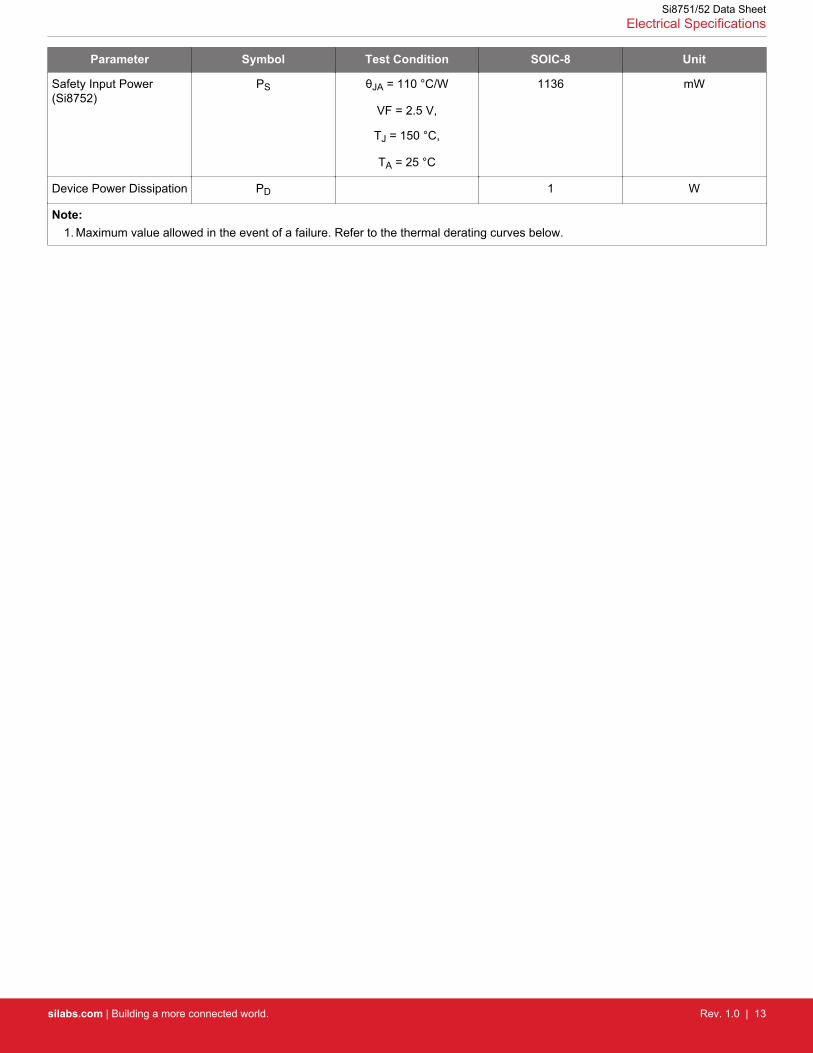
8. Top Markings
8.1 8-Pin Narrow Body SOIC
Table 8.1. Top Marking Explanation
Line 1 Marking: Customer Part Number Si875 = ISOdriver product series
X: 1 = Digital input, 2 = LED emulator input
A: Reserved
V: B = 2.5 kV isolation rating
Line 2 Marking: TTTTTT = Mfg code Manufacturing Code from Assembly Purchase Order form.
Line 3 Marking: YY = Year
WW = Work week
Assigned by the Assembly House. Corresponds to the year andworkweek of the mold date.
Si8751/52 Data SheetTop Markings
silabs.com | Building a more connected world. Rev. 1.0 | 24
9. Revision History
Revision 1.0, December 2017• Significant edits with production electrical specifications and load switching diagram.
Revision 0.5, September 2016• Significant edits with production electrical specifications.
Revision 0.1, May 2016
• Initial revision.
Si8751/52 Data SheetRevision History
silabs.com | Building a more connected world. Rev. 1.0 | 25

Table of Contents1. Ordering Guide . . . . . . . . . . . . . . . . . . . . . . . . . . . . . . 2
2. System Overview . . . . . . . . . . . . . . . . . . . . . . . . . . . . . . 32.1 Device Behavior . . . . . . . . . . . . . . . . . . . . . . . . . . . . . 4
2.2 Power Supply Connections (Si8751 Only) . . . . . . . . . . . . . . . . . . . . 5
2.3 TT Pin Description (Si8751 Only) . . . . . . . . . . . . . . . . . . . . . . . 5
2.4 LED Emulator Input (Si8752 Only) . . . . . . . . . . . . . . . . . . . . . . . 5
2.5 Output Description . . . . . . . . . . . . . . . . . . . . . . . . . . . . 6
2.6 Miller Clamp . . . . . . . . . . . . . . . . . . . . . . . . . . . . . . 62.6.1 Miller Clamp Description . . . . . . . . . . . . . . . . . . . . . . . . 62.6.2 Sizing Miller Clamp Capacitors . . . . . . . . . . . . . . . . . . . . . . 6
3. Applications. . . . . . . . . . . . . . . . . . . . . . . . . . . . . . . . 73.1 DC SSR Example . . . . . . . . . . . . . . . . . . . . . . . . . . . . 7
3.2 AC SSR Example . . . . . . . . . . . . . . . . . . . . . . . . . . . . 7
4. Electrical Specifications . . . . . . . . . . . . . . . . . . . . . . . . . . . 84.1 Test Circuits . . . . . . . . . . . . . . . . . . . . . . . . . . . . . .10
4.2 Regulatory Information . . . . . . . . . . . . . . . . . . . . . . . . . . .10
4.3 Typical Operating Characteristics . . . . . . . . . . . . . . . . . . . . . . .16
5. Pin Descriptions . . . . . . . . . . . . . . . . . . . . . . . . . . . . . 195.1 Si8751 Pin Descriptions . . . . . . . . . . . . . . . . . . . . . . . . . .19
5.2 Si8752 Pin Descriptions . . . . . . . . . . . . . . . . . . . . . . . . . .20
6. Package Outlines . . . . . . . . . . . . . . . . . . . . . . . . . . . . . 216.1 Package Outline: 8-Pin Narrow Body SOIC . . . . . . . . . . . . . . . . . . . .21
7. Land Patterns . . . . . . . . . . . . . . . . . . . . . . . . . . . . . . 237.1 Land Pattern: 8-Pin Narrow Body SOIC . . . . . . . . . . . . . . . . . . . . .23
8. Top Markings . . . . . . . . . . . . . . . . . . . . . . . . . . . . . . 248.1 8-Pin Narrow Body SOIC . . . . . . . . . . . . . . . . . . . . . . . . . .24
9. Revision History . . . . . . . . . . . . . . . . . . . . . . . . . . . . . 25
Table of Contents 26

http://www.silabs.com
Silicon Laboratories Inc.400 West Cesar ChavezAustin, TX 78701USA
Smart. Connected. Energy-Friendly.
Productswww.silabs.com/products
Qualitywww.silabs.com/quality
Support and Communitycommunity.silabs.com
DisclaimerSilicon Labs intends to provide customers with the latest, accurate, and in-depth documentation of all peripherals and modules available for system and software implementers using or intending to use the Silicon Labs products. Characterization data, available modules and peripherals, memory sizes and memory addresses refer to each specific device, and "Typical" parameters provided can and do vary in different applications. Application examples described herein are for illustrative purposes only. Silicon Labs reserves the right to make changes without further notice and limitation to product information, specifications, and descriptions herein, and does not give warranties as to the accuracy or completeness of the included information. Silicon Labs shall have no liability for the consequences of use of the information supplied herein. This document does not imply or express copyright licenses granted hereunder to design or fabricate any integrated circuits. The products are not designed or authorized to be used within any Life Support System without the specific written consent of Silicon Labs. A "Life Support System" is any product or system intended to support or sustain life and/or health, which, if it fails, can be reasonably expected to result in significant personal injury or death. Silicon Labs products are not designed or authorized for military applications. Silicon Labs products shall under no circumstances be used in weapons of mass destruction including (but not limited to) nuclear, biological or chemical weapons, or missiles capable of delivering such weapons.
Trademark InformationSilicon Laboratories Inc.® , Silicon Laboratories®, Silicon Labs®, SiLabs® and the Silicon Labs logo®, Bluegiga®, Bluegiga Logo®, Clockbuilder®, CMEMS®, DSPLL®, EFM®, EFM32®, EFR, Ember®, Energy Micro, Energy Micro logo and combinations thereof, "the world’s most energy friendly microcontrollers", Ember®, EZLink®, EZRadio®, EZRadioPRO®, Gecko®, ISOmodem®, Micrium, Precision32®, ProSLIC®, Simplicity Studio®, SiPHY®, Telegesis, the Telegesis Logo®, USBXpress®, Zentri and others are trademarks or registered trademarks of Silicon Labs. ARM, CORTEX, Cortex-M3 and THUMB are trademarks or registered trademarks of ARM Holdings. Keil is a registered trademark of ARM Limited. All other products or brand names mentioned herein are trademarks of their respective holders.