Embed Size (px)
Citation preview
Si53340-45 Data Sheet
Low-Jitter LVDS Fanout Clock Buffers with up to 10 LVDS Out-puts from Any-Format Input and Wide Frequency Range from dcup to 1250 MHzThe Si53340-45 family of LVDS fanout buffers is ideal for clock/data distribution and re-dundant clocking applications. These devices feature typical ultra-low jitter of 50 fs andoperate over a wide frequency range from dc to 1250 MHz. Built-in LDOs deliver highPSRR performance and reduces the need for external components simplifying low jitterclock distribution in noisy environments.
They are available in multiple configurations and offer a selectable input clock using a2:1 input mux. Other features include independent output enable and built-in formattranslation. These buffers can be paired with the Si534x clocks and Si5xx oscillators todeliver end-to-end clock tree performance.
KEY FEATURES
• Ultra-low additive jitter: 50 fs rms• Built-in LDOs for high PSRR performance• Up to 10 LVDS Outputs• Any-format Inputs (LVPECL, Low-Power
LVPECL, LVDS, CML, HCSL, LVCMOS)• Wide frequency range: dc to 1250 MHz• Output Enable option• Multiple configuration options• 2:1 Input Mux• RoHS compliant, Pb-free• Temperature range: –40 to +85 °C
0
1
CLK0*
CLK1*
CLK_SEL
*Si53341/43/45 require Single-ended Inputs
Si53342/43
Power Supply Filtering
VDD
4 Outputs
10 Outputs
4
10
3 Outputs
3 Outputs
3
3
OEAb
OEBb
VDDOA
VDDOB
Si53340/41
Si53344/45
silabs.com | Smart. Connected. Energy-friendly. Rev. 1.2

1. Ordering Guide
Table 1.1. Si5334x Ordering Guide
Part Number Input LVDS Output Output Enable (OE) Frequency Range Package
SI53340-B-GM 2:1 selectable MUXAny-format 1 bank / 4 Outputs — dc to 1250 MHz 16-QFN
3 x 3 mm
SI53341-B-GM 2:1 selectable MUXLVCMOS 1 bank / 4 Outputs — dc to 200 MHz 16-QFN
3 x 3 mm
SI53342-B-GM 2:1 selectable MUXAny-format 2 banks / 3 Outputs 1 per bank dc to 1250 MHz 24-QFN
4 x 4 mm
SI53343-B-GM 2:1 selectable MUXLVCMOS 2 banks / 3 Outputs 1 per bank dc to 200 MHz 24-QFN
4 x 4 mm
SI53344-B-GM 2:1 selectable MUXAny-format 1 bank / 10 Outputs — dc to 1250 MHz 32-QFN
5 x 5 mm
SI53345-B-GM 2:1 selectable MUXLVCMOS 1 bank / 10 Outputs — dc to 200 MHz 32-QFN
5 x 5 mm
Si53340-45 Data SheetOrdering Guide
silabs.com | Smart. Connected. Energy-friendly. Rev. 1.2 | 1

2. Functional Description
The Si53340-45 are a family of low-jitter, low skew, fixed format (LVDS) buffers. The Si53340/42/44 have a universal input that acceptsmost common differential or LVCMOS input signals, while the Si53341/43/45 accept only LVCMOS inputs. These devices are availablein multiple configurations customized for the end application (refer to 1. Ordering Guide for more details on configurations).
2.1 Universal, Any-Format Input Termination (Si53340/42/44)
The universal input stage enables simple interfacing to a wide variety of clock formats, including LVPECL, Low-power LVPECL, LVDS,CML, HCSL, and LVCMOS. The tables below summarize the various ac- and dc-coupling options supported by the device. For the besthigh-speed performance, the use of differential formats is recommended. For both single-ended and differential input clocks, the fastestpossible slew rate is recommended since low slew rates can increase the noise floor and degrade jitter performance. Though not re-quired, a minimum slew rate of 0.75 V/ns is recommended for differential formats and 1.0 V/ns for single-ended formats. See “AN766:Understanding and Optimizing Clock Buffer’s Additive Jitter Performance” for more information.
Table 2.1. Clock Input Options
Clock Format 1.8 V 2.5/3.3 V
AC-Coupled
LVPECL/Low-power LVPECL N/A Yes
LVCMOS No Yes
LVDS Yes Yes
HCSL No Yes (3.3 V)
CML Yes Yes
DC-Coupled
LVPECL/Low-power LVPECL N/A Yes
LVCMOS No Yes
LVDS No Yes
HCSL No Yes (3.3 V)
CML No No
Si53340-45 Data SheetFunctional Description
silabs.com | Smart. Connected. Energy-friendly. Rev. 1.2 | 2

Si53340/42/44
0.1 µF
0.1 µFCLKx
CLKxb100 �
VDD
Figure 2.1. Differential (HCSL, LVPECL, Low-Power LVPECL, LVDS, CML) AC-Coupled Input Termination
VDD
Si53340/42/44
VDD
1 k�
CMOSDriver
VTERM = VDD/2
CLKx
VDD = 3.3 V or 2.5 V
CLKxb50
Rs
1 k�DC-Coupled
VDD
Si53340/42/44
VDD
1 k�
CMOSDriver
VTERM = VDD/2
CLKx
VDD = 3.3 V or 2.5 V
CLKxb50
Rs
1 k�AC-Coupled
VDD
1 k�
1 k�
VBIAS = VDD/2
Note:Value for Rs should be chosen so that the total source impedance matches the characteristic impedance of the PCB trace.
Figure 2.2. Single-Ended (LVCMOS) Input Termination
Si53340-45 Data SheetFunctional Description
silabs.com | Smart. Connected. Energy-friendly. Rev. 1.2 | 3

VDD
Si53340/42/44
R1
VDD
R2
R1
R2
“Standard”LVPECL Driver
VTERM = VDD – 2VR1 // R2 = 50 Ohm
CLKx
= 3.3 V or 2.5 VVDD
3.3 V LVPECL: R1 = 127 Ohm, R2 = 82.5 Ohm
2.5 V LVPECL: R1 = 250 Ohm, R2 = 62.5 Ohm
DC Coupled LVPECL Input Termination Scheme 1
CLKxb
VDD
Si53340/42/44
VTERM = VDD – 2 V
= 3.3 V or 2.5 VVDD
“Standard”LVPECL Driver
CLKx
CLKxb
DC Coupled LVPECL Input Termination Scheme 2
VDD
Si53340/42/44
DC Coupled LVDS Input Termination
= 3.3 V or 2.5 VVDD
100 �Standard
LVDS Driver
CLKx
CLKxb
VDD
Si53340/42/4450 �
50 �
DC Coupled HCSL Input Termination Scheme
= 3.3 VVDD
StandardHCSL Driver
50 � 50 �
33 �CLKx
CLKxb
Note: 33 Ohm series termination is optional depending on the location of the receiver.
50 �
50 �
50 �
50 �
50 � 50 �
50 �
50 �
33 �
Figure 2.3. Differential DC-Coupled Input Terminations
Si53340-45 Data SheetFunctional Description
silabs.com | Smart. Connected. Energy-friendly. Rev. 1.2 | 4

2.2 LVCMOS Input Termination (Si53341/43/45)
The table below summarizes the various ac- and dc-coupling options supported by the LVCMOS device, and the figure shows the rec-ommended input clock termination.
Note: 1.8V LVCMOS inputs are not supported for Si53341/43/45.
Table 2.2. LVCMOS Input Clock Options
LVCMOS
AC-Coupled DC-Coupled
1.8 V No No
2.5/3.3 V Yes Yes
VDD
Si53341/43/45
CMOSDriver
CLKx
VDD = 3.3 V or 2.5 V
50 �Rs NC
DC-Coupled
VDD
Si53341/43/45
CMOSDriver
CLKx
VDD = 3.3 V or 2.5 V
50 �Rs NC
AC-Coupled
VDD
1 k�
1 k�
VBIAS = VDD/2
Note:Value for Rs should be chosen so that the total source impedance matches the characteristic impedance of the PCB trace.
Figure 2.4. Recommended Input Clock Termination (Si53341/43/45)
Si53340-45 Data SheetFunctional Description
silabs.com | Smart. Connected. Energy-friendly. Rev. 1.2 | 5

2.3 Input Bias Resistors
Internal bias resistors ensure a differential output low condition in the event that the clock inputs are not connected. The non-invertinginput is biased with a 18.75 kΩ pull-down to GND and a 75 kΩ pull-up to VDD. The inverting input is biased with a 75 kΩ pull-up to VDD.
RPU
CLK0 or CLK1
RPU
RPU = 75 k�RPD = 18.75 k�
RPD
+
–
VDD
Figure 2.5. Input Bias Resistors
Note: To minimize the possibility of system noise coupling into the Si5334x differential inputs and adversely affecting the buffered out-put, Silicon Labs recommends 1 PPS clocks and disabled/gapped clocks be DC-coupled and driven “stop-low” .
2.4 Input Mux
The Si5334x provide two clock inputs for applications that need to select between one of two clock sources. The CLK_SEL pin selectsthe active clock input. The following table summarizes the input and output clock based on the input mux and output enable pin set-tings.
Table 2.3. Input Mux Logic
CLK_SEL CLK0 CLK1 Q1 Qb
L L X L H
L H X H L
H X L L H
H X H H L
Note:1. On the next negative transition of CLK0 or CLK1.
Si53340-45 Data SheetFunctional Description
silabs.com | Smart. Connected. Energy-friendly. Rev. 1.2 | 6

2.5 Output Clock Termination Options
The recommended output clock termination options are shown below. Unused outputs should be left unconnected.
50
50
DC Coupled LVDS TerminationVDD
100 LVDS Receiver
Si5334x Q
Qb
VDDXX
50
50
0.1 µF
AC Coupled LVDS Termination
0.1 µF VDD
Si5334x Q
Qb
VDDXX
LVDS Receiver100
Note:For Si53340/41/44/45, VDDXX = VDD = 3.3 V, 2.5 V, 1.8 VFor Si53342/43, VDDXX = VDDOA or VDDOB = 3.3 V, 2.5 V, 1.8 V
Figure 2.6. LVDS Output Terminations
Si53340-45 Data SheetFunctional Description
silabs.com | Smart. Connected. Energy-friendly. Rev. 1.2 | 7

2.6 AC Timing Waveforms
QN
QM
TSK
TSK
TPLH
TR
TF
Q
Q
CLK
Q
TPHL
Output-Output SkewPropagation Delay
Rise/Fall Time
VPP/2
VPP/2
VPP/2
VPP/2
20% VPP
80% VPP 80% VPP20% VPP
Figure 2.7. AC Timing Waveforms
Si53340-45 Data SheetFunctional Description
silabs.com | Smart. Connected. Energy-friendly. Rev. 1.2 | 8

2.7 Typical Phase Noise Performance: Differential Input Clock
Each of the three phase noise plots superimposes Source Jitter, Total SE Jitter and Total Diff Jitter on the same diagram.• Source Jitter—Reference clock phase noise (measured Single-ended to PNA).• Total Jitter (SE)—Combined source and clock buffer phase noise measured as a single-ended output to the phase noise analyzer
and integrated from 12 kHz to 20 MHz.• Total Jitter (Diff)—Combined source and clock buffer phase noise measured as a differential output to the phase noise analyzer
and integrated from 12 kHz to 20 MHz. The differential measurement as shown in each figure is made using a balun. For more infor-mation, see 3. Electrical Specifications.
Note: To calculate the total RMS phase jitter when adding a buffer to your clock tree, use the root-sum-square (RSS).
CLKx50
50 Ohm
AG E5052 Phase Noise Analyzer
Si5334xDUT
CLK SYNTHSMA103A
Source jitter measured here
Total jitter measured here
Figure 2.8. Differential Measurement Method Using a Balun
The total jitter is a measure of the source plus the buffer's additive phase jitter. The additive jitter (rms) of the buffer can then be calcula-ted (via root-sum-square addition).
Frequency(MHz)
DifferentialInput Slew Rate (V/ns)
Source Jitter(fs)
Total Jitter(SE) (fs)
Additive Jitter(SE) (fs)
Total Jitter(Differential) (fs)
Additive Jitter(Differential) (fs)
156.25 1.0 38.2 147.8 142.8 118.3 112.0
Figure 2.9. Total Jitter Differential Input (156.25 MHz)
Si53340-45 Data SheetFunctional Description
silabs.com | Smart. Connected. Energy-friendly. Rev. 1.2 | 9

Frequency(MHz)
DifferentialInput Slew Rate (V/ns)
Source Jitter(fs)
Total Jitter(SE) (fs)
Additive Jitter(SE) (fs)
Total Jitter(Differential) (fs)
Additive Jitter(Differential) (fs)
312.5 1.0 33.10 94.39 88.39 83.80 76.99
Figure 2.10. Total Jitter Differential Input (312.5 MHz)
Frequency(MHz)
DifferentialInput Slew Rate (V/ns)
Source Jitter(fs)
Total Jitter(SE) (fs)
Additive Jitter(SE) (fs)
Total Jitter(Differential) (fs)
Additive Jitter(Differential) (fs)
625 1.0 23 57 52 59 54
Figure 2.11. Total Jitter Differential Input (625 MHz)
Si53340-45 Data SheetFunctional Description
silabs.com | Smart. Connected. Energy-friendly. Rev. 1.2 | 10
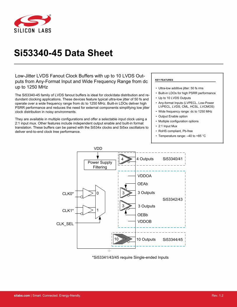
2.8 Typical Phase Noise Performance: Single-Ended Input Clock
For single-ended input phase noise measurements, the input was connected directly without the use of a balun.
The following figure shows three phase noise plots superimposed on the same diagram.
Frequency(MHz)
Single-EndedInput Slew Rate (V/ns)
Source Jitter(fs)
Total Jitter(SE) (fs)
Additive Jitter(SE) (fs)
Total Jitter(Differential) (fs)
Additive Jitter(Differential) (fs)
156.25 1.0 40.74 182.12 177.51 125.22 118.41
Figure 2.12. Total Jitter Single-Ended Input (156.25 MHz)
Si53340-45 Data SheetFunctional Description
silabs.com | Smart. Connected. Energy-friendly. Rev. 1.2 | 11

2.9 Input Mux Noise Isolation
The input clock mux is designed to minimize crosstalk between the CLK0 and CLK1. This improves phase jitter performance whenclocks are present at both the CLK0 and CLK1 inputs. The following figure shows a measurement of the input mux’s noise isolation.
Figure 2.13. Input Mux Noise Isolation (Differential Input Clock, 44-QFN Package)
Figure 2.14. Input Mux Noise Isolation (Single-Ended Input Clock, 24-QFN Package)
Si53340-45 Data SheetFunctional Description
silabs.com | Smart. Connected. Energy-friendly. Rev. 1.2 | 12

2.10 Power Supply Noise Rejection
The device supports on-chip supply voltage regulation to reject power supply noise and simplify low-jitter operation in real-world envi-ronments. This feature enables robust operation alongside FPGAs, ASICs and SoCs and may reduce board-level filtering requirements.See “AN491: Power Supply Rejection for Low-Jitter Clocks” for more information.
Si53340-45 Data SheetFunctional Description
silabs.com | Smart. Connected. Energy-friendly. Rev. 1.2 | 13

3. Electrical Specifications
Table 3.1. Recommended Operating Conditions
Parameter Symbol Test Condition Min Typ Max Unit
Ambient Operating Temperature TA –40 — 85 °C
Supply Voltage Range VDD LVDS
1.71 1.8 1.89 V
2.38 2.5 2.63 V
2.97 3.3 3.63 V
Table 3.2. Input Clock Specifications
VDD = 1.8 V, 2.5 V, or 3.3 V; TA = –40 to 85 °C
Parameter Symbol Test Condition Min Typ Max Unit
Differential Input CommonMode Voltage
VCM 0.05 — — V
Differential Input Swing (peak-to-peak)
VIN 0.2 — 2.2 V
Input High Voltage VIH VDD x 0.7 — — V
Input Low Voltage VIL — — VDD x 0.3 V
Input Capacitance CINCLK0 and CLK1 pins with re-
spect to GND — 5 — pF
Table 3.3. DC Common Characteristics
VDD = 1.8 V, 2.5 V, or 3.3 V; TA = –40 to 85 °C
Parameter Symbol Test Condition Min Typ Max Unit
Core Supply Current IDD1
Si53340/41 — 140 — mA
Si53342/43 — 80 — mA
Si53344/45 — 280 — mA
Output Supply Current(Per Clock Output) IDDO
1 Si53342/43 — 21 — mA
Input High Voltage VIH CLK_SEL, OEAb, OEBb VDD x 0.8 — — V
Input Low Voltage VIL CLK_SEL, OEAb, OEBb — — VDD x 0.2 V
Internal Pull-down Resistor RDOWN CLK_SEL, OEAb, OEBb — 25 — kΩ
Note:1. Measured using ac-coupled termination at VDD/VDDOX = 3.3 V.
Si53340-45 Data SheetElectrical Specifications
silabs.com | Smart. Connected. Energy-friendly. Rev. 1.2 | 14

Table 3.4. Output Characteristics (LVDS)
VDD = 1.8 V, 2.5 V, or 3.3 V; TA = –40 to 85 °C
Parameter Symbol Test Condition Min Typ Max Unit
Single-Ended Output Swing1 VSE RL = 100 Ω across QN and QbN 200 — 490 mV
Output Common Mode Voltage(VDD = 2.5 or 3.3 V) VCOM1
VDD = 2.38 to 2.63 V, 2.97 to 3.63 V,RL = 100 Ω across QN and QbN
1.10 1.25 1.35 V
Output Common Mode Voltage(VDD = 1.8 V)
VCOM2 VDD = 1.71 to 1.89 V,RL = 100 Ω across QN and QbN
0.83 0.97 1.25 V
Note:1. Unused outputs can be left floating. Do not short unused outputs to ground.
Table 3.5. AC Characteristics
VDD = 1.8 V ± 5%, 2.5 V ± 5%, or 3.3 V ±10%; TA = –40 to 85 °C
Parameter Symbol Test Condition Min Typ Max Unit
Frequency FSi53341/43/45 dc — 200 MHz
Si53340/42/44 dc — 1250 MHz
Duty Cycle(50% input duty cycle)
DC
20/80% TR/TF<10% of periodDifferential input clock
47 50 53 %
20/80% TR/TF<10% of period(Single-ended input clock)
45 50 55 %
Minimum Input Clock Slew Rate
SRdiffRequired to meet prop delay and ad-ditive jitter specifications (20–80%) 0.75 — — V/ns
SRse Required to meet prop delay and ad-ditive jitter specifications (20–80%)
1.00 — — V/ns
Output Rise/Fall Time TR/TF 20-80% — — 350 ps
Minimum Input Pulse Width TW 360 — — ps
Propagation Delay TPLH, TPHL 650 850 1050 ns
Output-to-Output Skew1 TSK — — 50 ps
Part-to-Part Skew2 TPS — — 125 ps
Power Supply Noise Rejection3 PSRR
10 kHz sinusoidal noise — –70 — dBc
100 kHz sinusoidal noise — –65 — dBc
500 kHz sinusoidal noise — –60 — dBc
1 MHz sinusoidal noise — –57.5 — dBc
Note:1. Output-to-output skew specified for outputs with identical configuration.2. Defined as skew between any output on different devices operating at the same supply voltage, temperature, and equal load con-
dition. Using the same type of inputs on each device, the outputs are measured at the differential cross points.3. Measured for 156.25 MHz carrier frequency. Sine-wave noise added to VDD (3.3 V = 100 mVPP) and noise spur amplitude meas-
ured. See “AN491: Power Supply Rejection for Low-Jitter Clocks” for more information.
Si53340-45 Data SheetElectrical Specifications
silabs.com | Smart. Connected. Energy-friendly. Rev. 1.2 | 15

Table 3.6. Additive Jitter, Differential Clock Input
VDD
Input1, 2 Output Additive Jitter (fs rms, 12kHz to 20 MHz)3
Freq (MHz) Clock FormatAmplitude VIN(Single-Ended,Peak-to-Peak)
Differential 20% to80% Slew Rate
(V/ns)Clock Format Typ Max
3.3 725 Differential 0.15 0.637 LVDS 50 65
3.3 156.25 Differential 0.5 0.458 LVDS 150 200
2.5 725 Differential 0.15 0.637 LVDS 50 65
2.5 156.25 Differential 0.5 0.458 LVDS 145 195
Note:1. For best additive jitter results, use the fastest slew rate possible. See “AN766: Understanding and Optimizing Clock Buffer’s Addi-
tive Jitter Performance” for more information.2. AC-coupled differential inputs.3. Measured differentially using a balun at the phase noise analyzer input. See Figure 1.
Table 3.7. Additive Jitter, Single-Ended Clock Input
VDD
Input1, 2 Output Additive Jitter (fs rms, 12kHz to 20 MHz)3
Freq (MHz) Clock FormatAmplitude VIN(Single-Ended,Peak-to-Peak)
Single-Ended 20%to 80% Slew Rate
(V/ns)Clock Format Typ Max
3.3 156.25 Single-ended 2.18 1 LVDS 150 200
2.5 156.25 Single-ended 2.18 1 LVDS 145 195
Note:1. For best additive jitter results, use the fastest slew rate possible. See “AN766: Understanding and Optimizing Clock Buffer’s Addi-
tive Jitter Performance” for more information.2. DC-coupled single-ended inputs.3. Measured differentially using a balun at the phase noise analyzer input. See figure below.
Table 3.8. Thermal Conditions
Parameter Symbol Test Condition Value Unit
16-QFN Thermal Resistance, Junction to Ambient θJA Still air 57.6 °C/W
16-QFN Thermal Resistance, Junction to Case θJC Still air 41.5 °C/W
24-QFN Thermal Resistance, Junction to Ambient θJA Still air 37 °C/W
24-QFN Thermal Resistance, Junction to Case θJC Still air 25 °C/W
32-QFN Thermal Resistance, Junction to Ambient θJA Still air 99.6 °C/W
32-QFN Thermal Resistance, Junction to Case θJC Still air 10.3 °C/W
Si53340-45 Data SheetElectrical Specifications
silabs.com | Smart. Connected. Energy-friendly. Rev. 1.2 | 16

Table 3.9. Absolute Maximum Ratings1
Parameter Symbol Test Condition Min Typ Max Unit
Storage Temperature TS –55 — 150 °C
Supply Voltage VDD –0.5 — 3.8 V
Input Voltage VIN –0.5 — VDD + 0.3 V
Output Voltage VOUT — — VDD + 0.3 V
ESD SensitivityHBM HBM, 100 pF, 1.5 kΩ — — 2000 V
CDM — — 500 V
Peak Soldering ReflowTemperature
TPEAKPb-Free; Solder reflow profile
per JEDEC J-STD-020 — — 260 °C
Maximum Junction Temperature TJ — — 125 °C
Note:1. Stresses beyond those listed in this table may cause permanent damage to the device. Functional operation specification compli-
ance is not implied at these conditions. Exposure to maximum rating conditions for extended periods may affect device reliability.
Si53340-45 Data SheetElectrical Specifications
silabs.com | Smart. Connected. Energy-friendly. Rev. 1.2 | 17

4. Detailed Block Diagrams
Q3
CLK0
CLK0b
CLK1
CLK1b
CLK_SEL
Q0
Q0b
Q1
Q1b
Q2
Q2b
Q3bSwitching Logic
Si53340
0
1
16-QFN 3x3 mm
Power Supply Filtering
VDD
Figure 4.1. Si53340 Block Diagram
Q3
CLK_SEL
Q0
Q0b
Q1
Q1b
Q2
Q2b
Q3bSwitching Logic
Si53341
0
1
16-QFN 3x3 mm
Power Supply Filtering
VDD
CLK0
CLK1
Figure 4.2. Si53341 Block Diagram
Si53340-45 Data SheetDetailed Block Diagrams
silabs.com | Smart. Connected. Energy-friendly. Rev. 1.2 | 18

Q4
Q3
Q0
Q0b
Q1
Q1b
Q2
Q2b
Q3b
Q4b
Si53342
OEAb
Q5
Q5b
OEBb
24-QFN 4x4 mm
VDDOA
VDDOB
Power Supply Filtering
VDD
CLK0
CLK0b
CLK1
CLK1b
CLK_SEL Switching Logic
0
1
Figure 4.3. Si53342 Block Diagram
Q4
Q3
Q0
Q0b
Q1
Q1b
Q2
Q2b
Q3b
Q4b
Si53343
OEAb
Q5
Q5b
OEBb
24-QFN 4x4 mm
VDDOA
VDDOB
Power Supply Filtering
VDD
CLK_SEL Switching Logic
0
1
CLK0
CLK1
Figure 4.4. Si53343 Block Diagram
Si53340-45 Data SheetDetailed Block Diagrams
silabs.com | Smart. Connected. Energy-friendly. Rev. 1.2 | 19

CLK_SEL Switching Logic
0
1
Q0
Q0bQ1
Q1bQ2
Q2bQ3
Q3bQ4
Q4bQ5
Q5bQ6
Q6bQ7
Q7bQ8
Q8bQ9
Q9bSi53344
32-QFN 5x5 mm
Power Supply Filtering
VDD
CLK0b
CLK1b
CLK0
CLK1
Figure 4.5. Si53344 Block Diagram
CLK0
CLK1
CLK_SEL Switching Logic
0
1
Q0
Q0bQ1
Q1bQ2
Q2bQ3
Q3bQ4
Q4bQ5
Q5bQ6
Q6bQ7
Q7bQ8
Q8bQ9
Q9bSi53345
32-QFN 5x5 mm
Power Supply Filtering
VDD
Figure 4.6. Si53345 Block Diagram
Si53340-45 Data SheetDetailed Block Diagrams
silabs.com | Smart. Connected. Energy-friendly. Rev. 1.2 | 20

5. Pin Descriptions
5.1 Si53340/41 Pin Descriptions
GND PAD
CLK
0
CLK
0bCLK1
CLK_SEL
Q3b
Q3
Q2b
Q2
Q1
NC
Q0b
CLK1b
GND Q1bV
DD
Q0
16 15 14 13
12
11
10
9
5 6 7 8
1
2
3
4
Si5334016-QFN
GND PAD
CLK
0
CLK1
CLK_SEL
Q3b
Q3
Q2b
Q2
Q1
NC
Q0b
GND Q1b
VD
D
Q0
16 15 14 13
12
11
10
9
5 6 7 8
1
2
3
4
Si5334116-QFN
NC
NC
Table 5.1. Si53340/41 16-QFN Pin Descriptions
Pin Name Type1 Description
1 GND GND Ground.
2 CLK_SEL I Mux input select pin (LVCMOS). When CLK_SEL is high, CLK1 is selected. WhenCLK_SEL is low, CLK0 is selected. CLK_SEL contains an internal pull-down resistor.
3 CLK1 I Input clock 1.
4
CLK1b(Si53340 only) I
Input clock 1 (complement). When CLK1 is driven by a single-ended LVCMOS input,connect CLK1b to an appropriate bias voltage (e.g., VDD/2.
NC(Si53341 only)
— No connect. Leave this pin unconnected.
5 VDD P Core and Output Voltage Supply. Bypass with 1.0 µF capacitor and place as close to theVDD pin as possible.
6 CLK0 I Input Clock 0.
7
CLK0b(Si53340 only) I
Input clock 0 (complement). When CLK0 is driven by a single-ended LVCMOS input,connect CLK0b to an appropriate bias voltage (e.g., VDD/2.
NC(Si53341 only)
— No connect. Leave this pin unconnected.
8 NC — No connect. Do not connect this pin.
9 Q0 O Output clock 0.
10 Q0b O Output clock 0 (complement).
11 Q1 O Output clock 1.
12 Q1b O Output clock 1 (complement).
13 Q2 O Output clock 2.
Si53340-45 Data SheetPin Descriptions
silabs.com | Smart. Connected. Energy-friendly. Rev. 1.2 | 21

Pin Name Type1 Description
14 Q2b O Output clock 2 (complement).
15 Q3 O Output clock 3.
16 Q3b O Output clock 3 (complement).
GND Pad ExposedGround Pad GND
Power supply ground and thermal relief. The exposed ground pad is thermally connectedto the die to improve heat transfer from the package. The ground pad must be connectedto GND to ensure device specifications are met.
Note:1. I = Input; O = Output; P = Power; GND = Ground.
Si53340-45 Data SheetPin Descriptions
silabs.com | Smart. Connected. Energy-friendly. Rev. 1.2 | 22

5.2 Si53342/43 Pin Descriptions
GND PAD
VDD
CLK
0b NC
CLK
1b
CLK_SEL
Q1
Q1b
VD
DO
A
Q2
Q2b
Q3
Q3b
VD
DO
BQ5b
Q4
NC
Q4b
Q0b
OEAb
CLK
1
OEBb
Q0
CLK
0
Q5
24 23 22 21 20 19
18
17
16
15
14
13
7 8 9 10 11 12
1
2
3
4
5
6
Si5334224-QFN
GND PAD
VDD
NC
CLK_SEL
Q1
Q1b
VD
DO
A
Q2
Q2b
Q3
Q3b
VD
DO
B
Q5b
Q4
NC
Q4b
Q0b
OEAb
CLK
1
OEBb
Q0
CLK
0
Q5
24 23 22 21 20 19
18
17
16
15
14
13
7 8 9 10 11 12
1
2
3
4
5
6
Si5334324-QFN
NC NC
Table 5.2. Si53342/43 24-QFN Pin Descriptions
Pin Name Type1 Description
1 OEAb I Output Enable for Bank A (Q0, Q1, Q2). When OEAb = LOW, outputs Q0, Q1, and Q2are enabled. This pin contains an active pull-down resistor, and leaving the pin discon-nected enables the outputs. When OEAb = HIGH, Q0, Q1, and Q2 are disabled.
2 Q1b O Output clock 1 (complement).
3 Q1 O Output clock 1.
4 Q0b O Output clock 0 (complement)
5 Q0 O Output clock 0
6 VDD P Core voltage supply. Bypass with 1.0 μF capacitor and place as close to the VDD pin aspossible.
7 CLK0 I Input clock 0.
8 CLK0b(Si53342 only)
O Input clock 0 (complement). When CLK0 is driven by a single-ended LVCMOS input,connect CLK0b to an appropriate bias voltage (e.g., VDD/2.
NC(Si53343 only)
— No connect. Leave this pin unconnected.
9 NC — No Connect. Do not connect this pin to anything.
10 NC — No Connect. Do not connect this pin to anything.
11 CLK1 I Input clock 1.
12 CLK1b(Si53342 only)
I Input clock 1 (complement). When CLK1 is driven by a single-ended LVCMOS input,connect CLK1b to an appropriate bias voltage (e.g., VDD/2.
NC(Si53343 only)
— No connect. Leave this pin unconnected.
Si53340-45 Data SheetPin Descriptions
silabs.com | Smart. Connected. Energy-friendly. Rev. 1.2 | 23

Pin Name Type1 Description
13 CLK_SEL I Mux input select pin (LVCMOS). When CLK_SEL is high, CLK1 is selected. WhenCLK_SEL is low, CLK0 is selected. CLK_SEL contains an internal pull-down resistor.
14 Q5b O Output clock 5 (complement).
15 Q5 O Output clock 5.
16 Q4b O Output clock 4 (complement).
17 Q4 O Output clock 4.
18 OEBb I Output Enable for Bank B (Q3, Q4, Q5). When OEBb = LOW, outputs Q3, Q4, and Q5are enabled. This pin contains an active pull-down resistor, and leaving the pin discon-nected enables the outputs. When OEBb = HIGH, Q3, Q4, and Q5 are disabled.
19 VDDOB P Output voltage spply—Bank B (Outputs: Q3 to Q5). Bypass with 1.0 µF capacitor andplace as close to the VDDOB pin as possible.
20 Q3b O Output clock 3 (complement).
21 Q3 O Output clock 3.
22 Q2b O Output clock 2 (complement).
23 Q2 O Output clock 2.
24 VDDOA P Output voltage supply—Bank A (Outputs: Q0 to Q2). Bypass with 1.0 μF capacitor andplace as close to the VDDOA pin as possible.
GND Pad ExposedGround Pad
GND Power supply ground and thermal relief. The exposed ground pad is thermally connectedto the die to improve heat transfer from the package. The ground pad must be connectedto GND to ensure device specifications are met.
Note:1. I = Input; O = Output; P = Power; GND = Ground.
Si53340-45 Data SheetPin Descriptions
silabs.com | Smart. Connected. Energy-friendly. Rev. 1.2 | 24

5.3 Si53344/45 Pin Descriptions
GND PAD
GND
Q9b Q
9
Q7
Q7b
VD
DQ6b
N/C
CLK0b
VD
D
Q0
Q0b
Q1
Q1b
Q2
Q2b
VD
D
Q6
Q4bQ
8b
Q5
CLK1
CLK_SEL
CLK0
Q8
Q3b
Q4
CLK1b
VDDV
DD
Q5b
Q332 31 30 29 28 27 26 25
24
23
22
21
20
19
18
17
9 10 11 12 13 14 15 16
1
2
3
4
5
6
7
8
Si5334432-QFN
GND PAD
GND
Q9b Q
9
Q7
Q7b
VD
D
Q6b
N/C
VD
D
Q0
Q0b
Q1
Q1b
Q2
Q2b
VD
D
Q6
Q4b
Q8b
Q5
CLK1
CLK_SEL
CLK0
Q8
Q3b
Q4
VDD
VD
D
Q5b
Q3
32 31 30 29 28 27 26 25
24
23
22
21
20
19
18
17
9 10 11 12 13 14 15 16
1
2
3
4
5
6
7
8
Si5334532-QFN
N/C
N/C
Table 5.3. Si53344/45 32-QFN Pin Descriptions
Pin # Name Type1 Description
1 VDD P Core and Output voltage supply. Bypass with 1.0 μF capacitor and place as close to theVDD pin as possible.
2 CLK_SEL I Mux input select pin (LVCMOS). When CLK_SEL is high, CLK1 is selected. WhenCLK_SEL is low, CLK0 is selected. CLK_SEL contains an internal pull-down resistor.
3 CLK0 I Input clock 0.
4
CLK0b(Si53344 only) I
Input clock 0 (complement). When CLK0 is driven by a single-ended LVCMOS input,connect CLK0b to an appropriate bias voltage (e.g., VDD/2.
NC(Si53345 only)
— No connect. Leave this pin unconnected.
5 NC No connect. Leave this pin unconnected.
6 CLK1 I Input clock 1.
7
CLK1b(Si53344 only) I
Input clock 1 (complement). When CLK1 is driven by a single-ended LVCMOS input,connect CLK1b to an appropriate bias voltage (e.g., VDD/2.
NC(Si53345 only)
— No connect. Leave this pin unconnected.
8 GND GND Ground.
9 VDD P Core and Output voltage supply. Bypass with 1.0 µF capacitor and place as closely tothe VDD pin as possible.
10 Q9b O Output clock 9 (complement).
11 Q9 O Output clock 9.
12 Q8b O Output clock 8 (complement).
13 Q8 O Output clock 8.
14 Q7b O Output clock 7 (complement).
Si53340-45 Data SheetPin Descriptions
silabs.com | Smart. Connected. Energy-friendly. Rev. 1.2 | 25

Pin # Name Type1 Description
15 Q7 O Output clock 7.
16 VDD P Core and Output voltage supply. Bypass with 1.0 µF capacitor and place as closely tothe VDD pin as possible.
17 Q6b O Output clock 6 (complement).
18 Q6 O Output clock 6.
19 Q5b O Output clock 5 (complement).
20 Q5 O Output clock 5.
21 Q4b O Output clock 4 (complement).
22 Q4 O Output clock 4.
23 Q3b O Output clock 3 (complement).
24 Q3 O Output clock 3.
25 VDD P Core and Output voltage supply. Bypass with 1.0 µF capacitor and place as closely tothe VDD pin as possible.
26 Q2b O Output clock 2 (complement).
27 Q2 O Output clock 2.
28 Q1b O Output clock 1 (complement).
29 Q1 O Output clock 1.
30 Q0b O Output clock 0 (complement).
31 Q0 O Output clock 0.
32 VDD P Core voltage supply. Bypass with 1.0 µF capacitor and place as closely to the VDD pinas possible.
GND Pad ExposedGround Pad GND
Power supply ground and thermal relief. The exposed ground pad is thermally connectedto the die to improve the heat transfer out of the package. The ground pad must be con-nected to GND to ensure device specifications are met.
Note:1. I = Input; O = Output; P = Power; GND = Ground.
Si53340-45 Data SheetPin Descriptions
silabs.com | Smart. Connected. Energy-friendly. Rev. 1.2 | 26

6. Package Outlines
6.1 16-Pin QFN Package
Figure 6.1. 16-Pin QFN Package
Table 6.1. 16-QFN Package Dimensions
Dimension Min Nom Max
A 0.80 0.85 0.90
A1 0.00 0.02 0.05
b 0.18 0.25 0.30
D 3.00 BSC.
D2 1.65 1.70 1.75
e 0.50 BSC.
E 3.00 BSC.
E2 1.65 1.70 1.75
L 0.30 0.40 0.50
aaa — — 0.10
bbb — — 0.10
ccc — — 0.08
ddd — — 0.10
eee — — 0.05
Note:1. All dimensions shown are in millimeters (mm) unless otherwise noted.2. Dimensioning and Tolerancing per ANSI Y14.5M-1994.
Si53340-45 Data SheetPackage Outlines
silabs.com | Smart. Connected. Energy-friendly. Rev. 1.2 | 27

6.2 24-Pin QFN Package
Figure 6.2. 24-Pin QFN Package
Table 6.2. 24-QFN Package Dimensions
Dimension Min Nom Max
A 0.80 0.85 0.90
A1 0.00 0.02 0.05
b 0.18 0.25 0.30
D 4.00 BSC.
D2 2.35 2.50 2.65
e 0.50 BSC.
E 4.00 BSC.
E2 2.35 2.50 2.65
L 0.30 0.40 0.50
aaa 0.10
bbb 0.10
ccc 0.08
ddd 0.10
eee 0.05
Note:1. All dimensions shown are in millimeters (mm) unless otherwise noted.2. Dimensioning and Tolerancing per ANSI Y14.5M-1994.3. This drawing conforms to JEDEC outline MO-220, variation VGGD-8.4. Recommended card reflow profile is per the JEDEC/IPC J-STD-020C specification for Small Body Components.
Si53340-45 Data SheetPackage Outlines
silabs.com | Smart. Connected. Energy-friendly. Rev. 1.2 | 28

6.3 32-Pin QFN Package
Figure 6.3. 32-Pin QFN Package
Table 6.3. 32-QFN Package Dimensions
Dimension Min Nom Max
A 0.80 0.85 1.00
A1 0.00 0.02 0.05
b 0.18 0.25 0.30
c 0.20 0.25 0.30
D 5.00 BSC
D2 2.00 2.15 2.30
e 0.50 BSC
E 5.00 BSC
E2 2.00 2.15 2.30
L 0.30 0.40 0.50
aaa 0.10
bbb 0.10
ccc 0.08
ddd 0.10
Note:1. All dimensions shown are in millimeters (mm) unless otherwise noted.2. Dimensioning and Tolerancing per ANSI Y14.5M-1994.3. This drawing conforms to the JEDEC Solid State Outline MO-220.
Si53340-45 Data SheetPackage Outlines
silabs.com | Smart. Connected. Energy-friendly. Rev. 1.2 | 29

7. Land Patterns
7.1 16-Pin QFN Land Pattern
Figure 7.1. 16-Pin QFN Land Pattern
Table 7.1. 16-QFN Land Pattern Dimensions
Dimension mm
C1 3.00
C2 3.00
E 0.50
X1 0.30
Y1 0.80
X2 1.75
Y2 1.75
Notes:
General1. All dimensions shown are in millimeters (mm).2. This Land Pattern Design is based on the IPC-7351 guidelines.3. All dimensions shown are at Maximum Material Condition (MMC). Least Material Condition (LMC) is calculated based on a Fabri-
cation Allowance of 0.05 mm.
Solder Mask Design1. All metal pads are to be non-solder mask defined (NSMD). Clearance between the solder mask and the metal pad is to be 60 µm
minimum, all the way around the pad.
Stencil Design1. A stainless steel, laser-cut and electro-polished stencil with trapezoidal walls should be used to assure good solder paste release.2. The stencil thickness should be 0.125 mm (5 mils).3. The ratio of stencil aperture to land pad size should be 1:1 for all perimeter pads.4. A 2 x 2 array of 0.65 mm square openings on a 0.90 mm pitch should be used for the center ground pad.
Card Assembly1. A No-Clean, Type-3 solder paste is recommended.2. The recommended card reflow profile is per the JEDEC/IPC J-STD-020 specification for Small Body Components.
Si53340-45 Data SheetLand Patterns
silabs.com | Smart. Connected. Energy-friendly. Rev. 1.2 | 30

7.2 24-Pin QFN Land Pattern
Figure 7.2. 24-Pin QFN Land Pattern
Table 7.2. 24-QFN Land Pattern Dimensions
Dimension mm
P1 2.55
P2 2.55
X1 0.25
Y1 0.80
C1 3.90
C2 3.90
E 0.50
Notes:
General1. All dimensions shown are in millimeters (mm).2. This Land Pattern Design is based on the IPC-7351 guidelines.
Solder Mask Design1. All metal pads are to be non-solder mask defined (NSMD). Clearance between the solder mask and the metal pad is to be 60 m
minimum, all the way around the pad.
Stencil Design1. A stainless steel, laser-cut and electro-polished stencil with trapezoidal walls should be used to assure good solder paste release.2. The stencil thickness should be 0.125 mm (5 mils).3. The ratio of stencil aperture to land pad size should be 1:1 for all perimeter pads.4. A 2 x 2 array of 1.10 mm x 1.10 mm openings on 1.30 mm pitch should be used for the center ground pad.
Card Assembly1. A No-Clean, Type-3 solder paste is recommended.2. The recommended card reflow profile is per the JEDEC/IPC J-STD-020 specification for Small Body Components.
Si53340-45 Data SheetLand Patterns
silabs.com | Smart. Connected. Energy-friendly. Rev. 1.2 | 31

7.3 32-Pin QFN Land Pattern
Figure 7.3. 32-Pin QFN Land Pattern
Table 7.3. 32-QFN Land Pattern Dimensions
Dimension Min Max Dimension Min Max
C1 4.52 4.62 X2 2.20 2.30
C2 4.52 4.62 Y1 0.59 0.69
E 0.50 BSC Y2 2.20 2.30
X1 0.20 0.30
Notes:
General1. All dimensions shown are in millimeters (mm) unless otherwise noted.2. This Land Pattern Design is based on the IPC-7351 guidelines.
Solder Mask Design1. All metal pads are to be non-solder mask defined (NSMD). Clearance between the solder mask and the metal pad is to be 60 mm
minimum, all the way around the pad.
Stencil Design1. A stainless steel, laser-cut and electro-polished stencil with trapezoidal walls should be used to assure good solder paste release.2. The stencil thickness should be 0.125 mm (5 mils).3. The ratio of stencil aperture to land pad size should be 1:1 for all perimeter pads.4. A 2 x 2 array of 0.75 mm square openings on 1.15 mm pitch should be used for the center ground pad.
Card Assembly1. A No-Clean, Type-3 solder paste is recommended.2. The recommended card reflow profile is per the JEDEC/IPC J-STD-020 specification for Small Body Components.
Si53340-45 Data SheetLand Patterns
silabs.com | Smart. Connected. Energy-friendly. Rev. 1.2 | 32

8. Top Markings
8.1 Si53340/41 To Markings
Figure 8.1. Si53340 Top Marking Figure 8.2. Si53341 Top Marking
Table 8.1. Si53340/41 Top Marking Explanation
Mark Method: Laser
Font Size: 0.635 mm (25 mils) Right-Justified
Line 1 Marking: Product ID 3340 for Si53340; 3341 for Si53341
Line 2 Marking: TTTT = Mfg Code Manufacturing Code
Line 3 Marking Circle = 0.5 mm Diameter Bottom-Left Justified
Pin 1 Identifier
YWW = Date Code Corresponds to the last digit of the current year (Y) and the work-week (WW) of the mold date.
Si53340-45 Data SheetTop Markings
silabs.com | Smart. Connected. Energy-friendly. Rev. 1.2 | 33

8.2 Si53342/43 Top Markings
Figure 8.3. Si53342 Top Marking Figure 8.4. Si53343 Top Marking
Table 8.2. Si53342/43 Top Marking Explanation
Mark Method: Laser
Font Size: 2.0 Point (28 mils) Center-Justified
Line 1 Marking: Device Part Number Si53342 for Si53342; Si53343 for Si53343
Line 2 Marking: Device Revision/Type B-GM
Line 3 Marking: TTTTTT = Mfg Code Manufacturing Code from the Assembly Purchase Order form.
Line 4 Marking: Circle = 0.5 mm Diameter Lower-LeftJustified
Pin 1 Identifier
YY = year WW = Work Week Assigned by the Assembly House. Corresponds to the year andwork week of the mold date.
Si53340-45 Data SheetTop Markings
silabs.com | Smart. Connected. Energy-friendly. Rev. 1.2 | 34

8.3 Si53344/45 Top Markings
Figure 8.5. Si53344 Top Marking Figure 8.6. Si53345 Top Marking
Table 8.3. Si53344/45 Top Marking Explanation
Mark Method: Laser
Font Size: 2.0 Point (28 mils) Center-Justified
Line 1 Marking: Device Part Number 53344 for Si53344; 53345 for Si53345
Line 2 Marking: Device Revision/Type B-GM
Line 3 Marking: TTTTTT = Mfg Code Manufacturing Code from the Assembly Purchase Order form.
Line 4 Marking: Circle = 0.5 mm Diameter Lower-LeftJustified
Pin 1 Identifier
YY = year WW = Work Week Assigned by the Assembly House. Corresponds to the year andwork week of the mold date.
Si53340-45 Data SheetTop Markings
silabs.com | Smart. Connected. Energy-friendly. Rev. 1.2 | 35

Table of Contents1. Ordering Guide . . . . . . . . . . . . . . . . . . . . . . . . . . . . . . 1
2. Functional Description. . . . . . . . . . . . . . . . . . . . . . . . . . . . 22.1 Universal, Any-Format Input Termination (Si53340/42/44) . . . . . . . . . . . . . . . 2
2.2 LVCMOS Input Termination (Si53341/43/45) . . . . . . . . . . . . . . . . . . . 5
2.3 Input Bias Resistors . . . . . . . . . . . . . . . . . . . . . . . . . . . . 6
2.4 Input Mux . . . . . . . . . . . . . . . . . . . . . . . . . . . . . . . 6
2.5 Output Clock Termination Options . . . . . . . . . . . . . . . . . . . . . . . 7
2.6 AC Timing Waveforms . . . . . . . . . . . . . . . . . . . . . . . . . . . 8
2.7 Typical Phase Noise Performance: Differential Input Clock . . . . . . . . . . . . . . . 9
2.8 Typical Phase Noise Performance: Single-Ended Input Clock . . . . . . . . . . . . . .11
2.9 Input Mux Noise Isolation . . . . . . . . . . . . . . . . . . . . . . . . . .12
2.10 Power Supply Noise Rejection . . . . . . . . . . . . . . . . . . . . . . . .13
3. Electrical Specifications . . . . . . . . . . . . . . . . . . . . . . . . . . 14
4. Detailed Block Diagrams . . . . . . . . . . . . . . . . . . . . . . . . . . 18
5. Pin Descriptions . . . . . . . . . . . . . . . . . . . . . . . . . . . . . 215.1 Si53340/41 Pin Descriptions . . . . . . . . . . . . . . . . . . . . . . . . .21
5.2 Si53342/43 Pin Descriptions . . . . . . . . . . . . . . . . . . . . . . . . .23
5.3 Si53344/45 Pin Descriptions . . . . . . . . . . . . . . . . . . . . . . . . .25
6. Package Outlines . . . . . . . . . . . . . . . . . . . . . . . . . . . . . 276.1 16-Pin QFN Package . . . . . . . . . . . . . . . . . . . . . . . . . . .27
6.2 24-Pin QFN Package . . . . . . . . . . . . . . . . . . . . . . . . . . .28
6.3 32-Pin QFN Package . . . . . . . . . . . . . . . . . . . . . . . . . . .29
7. Land Patterns . . . . . . . . . . . . . . . . . . . . . . . . . . . . . . 307.1 16-Pin QFN Land Pattern . . . . . . . . . . . . . . . . . . . . . . . . . .30
7.2 24-Pin QFN Land Pattern . . . . . . . . . . . . . . . . . . . . . . . . . .31
7.3 32-Pin QFN Land Pattern . . . . . . . . . . . . . . . . . . . . . . . . . .32
8. Top Markings . . . . . . . . . . . . . . . . . . . . . . . . . . . . . . 338.1 Si53340/41 To Markings . . . . . . . . . . . . . . . . . . . . . . . . . .33
8.2 Si53342/43 Top Markings . . . . . . . . . . . . . . . . . . . . . . . . . .34
8.3 Si53344/45 Top Markings . . . . . . . . . . . . . . . . . . . . . . . . . .35
Table of Contents . . . . . . . . . . . . . . . . . . . . . . . . . . . . . . 36
Table of Contents 36

http://www.silabs.com
Silicon Laboratories Inc.400 West Cesar ChavezAustin, TX 78701USA
ClockBuilder ProOne-click access to Timing tools, documentation, software, source code libraries & more. Available for Windows and iOS (CBGo only).
www.silabs.com/CBPro
Timing Portfoliowww.silabs.com/timing
SW/HWwww.silabs.com/CBPro
Qualitywww.silabs.com/quality
Support and Communitycommunity.silabs.com
DisclaimerSilicon Labs intends to provide customers with the latest, accurate, and in-depth documentation of all peripherals and modules available for system and software implementers using or intending to use the Silicon Labs products. Characterization data, available modules and peripherals, memory sizes and memory addresses refer to each specific device, and "Typical" parameters provided can and do vary in different applications. Application examples described herein are for illustrative purposes only. Silicon Labs reserves the right to make changes without further notice and limitation to product information, specifications, and descriptions herein, and does not give warranties as to the accuracy or completeness of the included information. Silicon Labs shall have no liability for the consequences of use of the information supplied herein. This document does not imply or express copyright licenses granted hereunder to design or fabricate any integrated circuits. The products are not designed or authorized to be used within any Life Support System without the specific written consent of Silicon Labs. A "Life Support System" is any product or system intended to support or sustain life and/or health, which, if it fails, can be reasonably expected to result in significant personal injury or death. Silicon Labs products are not designed or authorized for military applications. Silicon Labs products shall under no circumstances be used in weapons of mass destruction including (but not limited to) nuclear, biological or chemical weapons, or missiles capable of delivering such weapons.
Trademark InformationSilicon Laboratories Inc.® , Silicon Laboratories®, Silicon Labs®, SiLabs® and the Silicon Labs logo®, Bluegiga®, Bluegiga Logo®, Clockbuilder®, CMEMS®, DSPLL®, EFM®, EFM32®, EFR, Ember®, Energy Micro, Energy Micro logo and combinations thereof, "the world’s most energy friendly microcontrollers", Ember®, EZLink®, EZRadio®, EZRadioPRO®, Gecko®, ISOmodem®, Precision32®, ProSLIC®, Simplicity Studio®, SiPHY®, Telegesis, the Telegesis Logo®, USBXpress® and others are trademarks or registered trademarks of Silicon Labs. ARM, CORTEX, Cortex-M3 and THUMB are trademarks or registered trademarks of ARM Holdings. Keil is a registered trademark of ARM Limited. All other products or brand names mentioned herein are trademarks of their respective holders.