Embed Size (px)
Citation preview

Skyworks Solutions, Inc. • Phone [781] 376-3000 • Fax [781] 376-3100 • [email protected] • www.skyworksinc.comRev. 1.4 • Skyworks Proprietary Information • Products and Product Information are Subject to Change Without Notice • September 27, 2021
Si533
DUAL-FREQUENCY CRYSTAL OSCILLATOR (XO)(10 MHZ TO 1.4 GHZ)
Features
Applications
Description
The Si533 dual frequency XO utilizes Skyworks Solutions’ advancedDSPLL® circuitry to provide a low jitter clock at high frequencies. The Si533is available with any-frequency output frequency from 10 to 945 MHz andselect frequencies to 1400 MHz. Unlike a traditional XO, where a differentcrystal is required for each output frequency, the Si533 uses one fixed crystalto provide a wide range of output frequencies. This IC based approach allowsthe crystal resonator to provide exceptional frequency stability and reliability.In addition, DSPLL clock synthesis provides superior supply noise rejection,simplifying the task of generating low jitter clocks in noisy environmentstypically found in communication systems. The Si533 IC based XO is factoryconfigurable for a wide variety of user specifications including frequency,supply voltage, output format, and temperature stability. Specificconfigurations are factory programmed at time of shipment, therebyeliminating long lead times associated with custom oscillators.
Functional Block Diagram
Available with any-frequency output frequencies from 10 MHz to 945 MHz and select frequencies to 1.4 GHz
2 selectable output frequencies 3rd generation DSPLL® with superior
jitter performance 3x better frequency stability than
SAW-based oscillators Pin 1 output enable (OE)
Internal fixed crystal frequency ensures high reliability and low aging
Available CMOS, LVPECL, LVDS, and CML outputs
3.3, 2.5, and 1.8 V supply options Industry-standard 5 x 7 mm
package and pinout Pb-free/RoHS-compliant
SONET/SDH Networking SD/HD video
Clock and data recovery FPGA/ASIC clock generation
Any-frequency10–1400 MHz
DSPLL® Clock
Synthesis
VDD CLK+CLK–
OE GNDFS
Fixed Frequency
XO
Ordering Information:
See page 7.
Pin Assignments:
See page 6.
(Top View)
Si5602
1
2
3
6
5
4GND
FS
VDD
CLK+
CLK–
OE
1
2
3
6
5
4GND
FS
VDD
CLK+
NC
OE
LVDS/LVPECL/CML
CMOS
REVISION D

Si533
2 Skyworks Solutions, Inc. • Phone [781] 376-3000 • Fax [781] 376-3100 • [email protected] • www.skyworksinc.comRev. 1.4 • Skyworks Proprietary Information • Products and Product Information are Subject to Change Without Notice • September 27, 2021
1. Electrical Specifications
Table 1. Recommended Operating Conditions
Parameter Symbol Test Condition Min Typ Max Units
Supply Voltage1 VDD 3.3 V option 2.97 3.3 3.63 V
2.5 V option 2.25 2.5 2.75 V
1.8 V option 1.71 1.8 1.89 V
Supply Current IDD Output enabledLVPECL
CMLLVDSCMOS
————
111999081
1211089888
mA
Tristate mode — 60 75 mA
Output Enable (OE) and Frequency Select (FS)2
VIH 0.75 x VDD — — V
VIL — — 0.5 V
Operating Temperature Range TA –40 — 85 ºC
Notes:1. Selectable parameter specified by part number. See Section 3. "Ordering Information" on page 7 for further details.2. OE and FS pins include a 17 k pullup resistor to VDD.
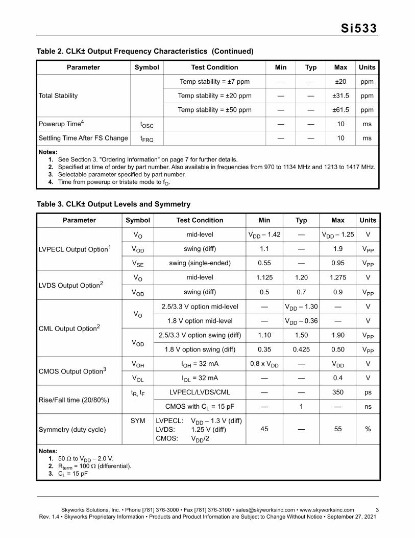
Table 2. CLK± Output Frequency Characteristics
Parameter Symbol Test Condition Min Typ Max Units
Nominal Frequency1,2 fO LVPECL/LVDS/CML 10 — 945 MHz
CMOS 10 — 160 MHz
Initial Accuracyfi
Measured at +25 °C at time of shipping
— ±1.5 — ppm
Temperature Stability1,3–7
–20–50
———
+7+20+50
ppm
Aging faFrequency drift over first year — — ±3 ppm
Frequency drift over 20 year life — — ±10 ppm
Notes:1. See Section 3. "Ordering Information" on page 7 for further details.2. Specified at time of order by part number. Also available in frequencies from 970 to 1134 MHz and 1213 to 1417 MHz.3. Selectable parameter specified by part number.4. Time from powerup or tristate mode to fO.
Si533
Skyworks Solutions, Inc. • Phone [781] 376-3000 • Fax [781] 376-3100 • [email protected] • www.skyworksinc.com 3Rev. 1.4 • Skyworks Proprietary Information • Products and Product Information are Subject to Change Without Notice • September 27, 2021
Total Stability
Temp stability = ±7 ppm — — ±20 ppm
Temp stability = ±20 ppm — — ±31.5 ppm
Temp stability = ±50 ppm — — ±61.5 ppm
Powerup Time4 tOSC — — 10 ms
Settling Time After FS Change tFRQ — — 10 ms
Table 3. CLK± Output Levels and Symmetry
Parameter Symbol Test Condition Min Typ Max Units
LVPECL Output Option1
VO mid-level VDD – 1.42 — VDD – 1.25 V
VOD swing (diff) 1.1 — 1.9 VPP
VSE swing (single-ended) 0.55 — 0.95 VPP
LVDS Output Option2VO mid-level 1.125 1.20 1.275 V
VOD swing (diff) 0.5 0.7 0.9 VPP
CML Output Option2
VO
2.5/3.3 V option mid-level — VDD – 1.30 — V
1.8 V option mid-level — VDD – 0.36 — V
VOD
2.5/3.3 V option swing (diff) 1.10 1.50 1.90 VPP
1.8 V option swing (diff) 0.35 0.425 0.50 VPP
CMOS Output Option3VOH IOH = 32 mA 0.8 x VDD — VDD V
VOL IOL = 32 mA — — 0.4 V
Rise/Fall time (20/80%)tR, tF LVPECL/LVDS/CML — — 350 ps
CMOS with CL = 15 pF — 1 — ns
Symmetry (duty cycle)SYM LVPECL: VDD – 1.3 V (diff)
LVDS: 1.25 V (diff)CMOS: VDD/2
45 — 55 %
Notes:1. 50 to VDD – 2.0 V.2. Rterm = 100 (differential).3. CL = 15 pF
Table 2. CLK± Output Frequency Characteristics (Continued)
Parameter Symbol Test Condition Min Typ Max Units
Notes:1. See Section 3. "Ordering Information" on page 7 for further details.2. Specified at time of order by part number. Also available in frequencies from 970 to 1134 MHz and 1213 to 1417 MHz.3. Selectable parameter specified by part number.4. Time from powerup or tristate mode to fO.
Si533
4 Skyworks Solutions, Inc. • Phone [781] 376-3000 • Fax [781] 376-3100 • [email protected] • www.skyworksinc.comRev. 1.4 • Skyworks Proprietary Information • Products and Product Information are Subject to Change Without Notice • September 27, 2021
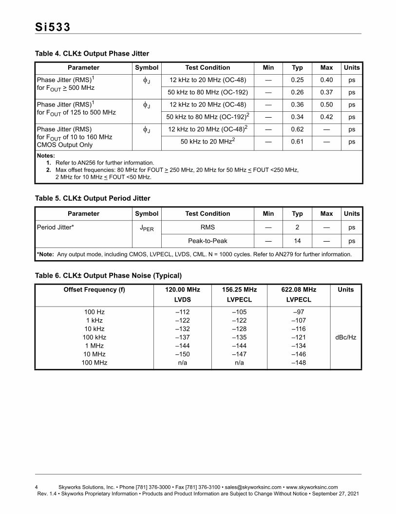
Table 4. CLK± Output Phase Jitter
Parameter Symbol Test Condition Min Typ Max Units
Phase Jitter (RMS)1
for FOUT > 500 MHzJ 12 kHz to 20 MHz (OC-48) — 0.25 0.40 ps
50 kHz to 80 MHz (OC-192) — 0.26 0.37 ps
Phase Jitter (RMS)1 for FOUT of 125 to 500 MHz
J 12 kHz to 20 MHz (OC-48) — 0.36 0.50 ps
50 kHz to 80 MHz (OC-192)2 — 0.34 0.42 ps
Phase Jitter (RMS) for FOUT of 10 to 160 MHzCMOS Output Only
J 12 kHz to 20 MHz (OC-48)2 — 0.62 — ps
50 kHz to 20 MHz2 — 0.61 — ps
Notes:1. Refer to AN256 for further information.2. Max offset frequencies: 80 MHz for FOUT > 250 MHz, 20 MHz for 50 MHz < FOUT <250 MHz,
2 MHz for 10 MHz < FOUT <50 MHz.
Table 5. CLK± Output Period Jitter
Parameter Symbol Test Condition Min Typ Max Units
Period Jitter* JPER RMS — 2 — ps
Peak-to-Peak — 14 — ps
*Note: Any output mode, including CMOS, LVPECL, LVDS, CML. N = 1000 cycles. Refer to AN279 for further information.
Table 6. CLK± Output Phase Noise (Typical)
Offset Frequency (f) 120.00 MHz
LVDS
156.25 MHz
LVPECL
622.08 MHz
LVPECL
Units
100 Hz1 kHz10 kHz
100 kHz1 MHz10 MHz100 MHz
–112–122–132–137–144–150n/a
–105–122–128–135–144–147n/a
–97–107–116–121–134–146–148
dBc/Hz
Si533
Skyworks Solutions, Inc. • Phone [781] 376-3000 • Fax [781] 376-3100 • [email protected] • www.skyworksinc.com 5Rev. 1.4 • Skyworks Proprietary Information • Products and Product Information are Subject to Change Without Notice • September 27, 2021
Table 7. Environmental ComplianceThe Si533 meets the following qualification test requirements.
Parameter Conditions/Test Method
Mechanical Shock MIL-STD-883, Method 2002
Mechanical Vibration MIL-STD-883, Method 2007
Solderability MIL-STD-883, Method 2003
Gross & Fine Leak MIL-STD-883, Method 1014
Resistance to Solder Heat MIL-STD-883, Method 2036
Moisture Sensitivity Level J-STD_020, MSL1
Contact Pads Gold over Nickel
Table 8. Thermal Characteristics(Typical values TA = 25 ºC, VDD = 3.3 V)
Parameter Symbol Test Condition Min Typ Max Unit
Thermal Resistance Junction to Ambient JA Still Air — 84.6 — °C/W
Thermal Resistance Junction to Case JC Still Air — 38.8 — °C/W
Ambient Temperature TA –40 — 85 °C
Junction Temperature TJ — — 125 °C
Table 9. Absolute Maximum Ratings1
Parameter Symbol Rating Units
Maximum Operating Temperature TAMAX 85 ºC
Supply Voltage, 1.8 V Option VDD –0.5 to +1.9 V
Supply Voltage, 2.5/3.3 V Option VDD –0.5 to +3.8 V
Input Voltage (any input pin) VI –0.5 to VDD + 0.3 V
Storage Temperature TS –55 to +125 ºC
ESD Sensitivity (HBM, per JESD22-A114) ESD 2500 V
Soldering Temperature (Pb-free profile)2 TPEAK 260 ºC
Soldering Temperature Time @ TPEAK (Pb-free profile)2 tP 20–40 seconds
Notes:1. Stresses beyond those listed in Absolute Maximum Ratings may cause permanent damage to the device. Functional
operation or specification compliance is not implied at these conditions. Exposure to maximum rating conditions for extended periods may affect device reliability.
2. The device is compliant with JEDEC J-STD-020C. Refer to Si5xx Packaging FAQ available for download at https://www.skyworksinc.com/Product_Certificate.aspx for further information, including soldering profiles.
Si533
6 Skyworks Solutions, Inc. • Phone [781] 376-3000 • Fax [781] 376-3100 • [email protected] • www.skyworksinc.comRev. 1.4 • Skyworks Proprietary Information • Products and Product Information are Subject to Change Without Notice • September 27, 2021
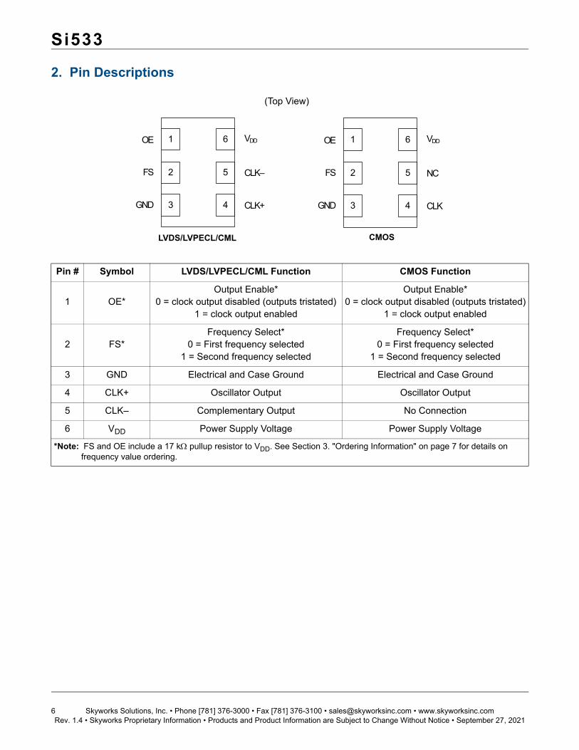
2. Pin Descriptions
Pin # Symbol LVDS/LVPECL/CML Function CMOS Function
1 OE*Output Enable*
0 = clock output disabled (outputs tristated)1 = clock output enabled
Output Enable*0 = clock output disabled (outputs tristated)
1 = clock output enabled
2 FS*Frequency Select*
0 = First frequency selected1 = Second frequency selected
Frequency Select*0 = First frequency selected
1 = Second frequency selected
3 GND Electrical and Case Ground Electrical and Case Ground
4 CLK+ Oscillator Output Oscillator Output
5 CLK– Complementary Output No Connection
6 VDD Power Supply Voltage Power Supply Voltage
*Note: FS and OE include a 17 k pullup resistor to VDD. See Section 3. "Ordering Information" on page 7 for details on frequency value ordering.
1
2
3
6
5
4GND
FS
VDD
CLK+
CLK–
OE
(Top View)
1
2
3
6
5
4GND
FS
VDD
CLK
NC
OE
LVDS/LVPECL/CML CMOS
Si533
Skyworks Solutions, Inc. • Phone [781] 376-3000 • Fax [781] 376-3100 • [email protected] • www.skyworksinc.com 7Rev. 1.4 • Skyworks Proprietary Information • Products and Product Information are Subject to Change Without Notice • September 27, 2021
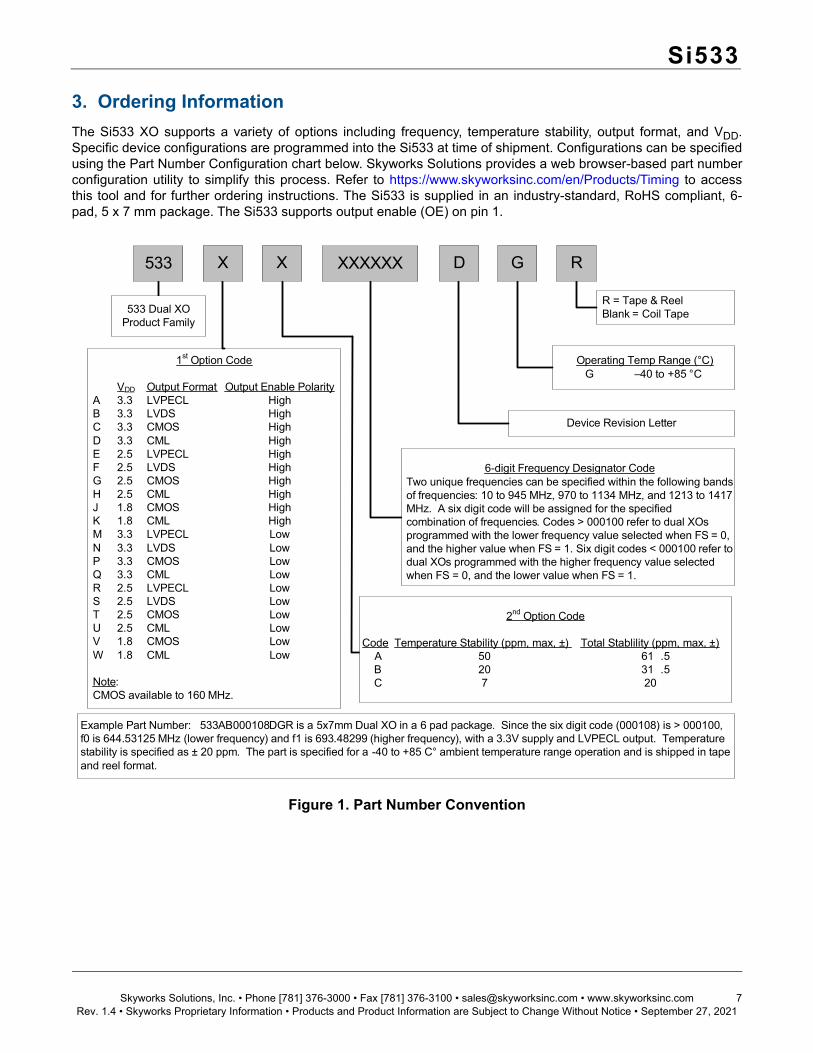
3. Ordering Information
The Si533 XO supports a variety of options including frequency, temperature stability, output format, and VDD.Specific device configurations are programmed into the Si533 at time of shipment. Configurations can be specifiedusing the Part Number Configuration chart below. Skyworks Solutions provides a web browser-based part numberconfiguration utility to simplify this process. Refer to https://www.skyworksinc.com/en/Products/Timing to accessthis tool and for further ordering instructions. The Si533 is supplied in an industry-standard, RoHS compliant, 6-pad, 5 x 7 mm package. The Si533 supports output enable (OE) on pin 1.
Figure 1. Part Number Convention
Example Part Number: 533AB000108DGR is a 5x7mm Dual XO in a 6 pad package. Since the six digit code (000108) is > 000100, f0 is 644.53125 MHz (lower frequency) and f1 is 693.48299 (higher frequency), with a 3.3V supply and LVPECL output. Temperature stability is specified as ± 20 ppm. The part is specified for a -40 to +85 C° ambient temperature range operation and is shipped in tape and reel format.
R = Tape & ReelBlank = Coil Tape
Operating Temp Range (°C)G –40 to +85 °C
Device Revision Letter
533 Dual XO Product Family
6-digit Frequency Designator CodeTwo unique frequencies can be specified within the following bands of frequencies: 10 to 945 MHz, 970 to 1134 MHz, and 1213 to 1417 MHz. A six digit code will be assigned for the specified combination of frequencies. Codes > 000100 refer to dual XOs programmed with the lower frequency value selected when FS = 0, and the higher value when FS = 1. Six digit codes < 000100 refer to dual XOs programmed with the higher frequency value selected when FS = 0, and the lower value when FS = 1.
533 X X XXXXXX D G R
1st Option Code
VDD Output Format Output Enable PolarityA 3.3 LVPECL HighB 3.3 LVDS High C 3.3 CMOS HighD 3.3 CML HighE 2.5 LVPECL HighF 2.5 LVDS HighG 2.5 CMOS HighH 2.5 CML HighJ 1.8 CMOS HighK 1.8 CML HighM 3.3 LVPECL LowN 3.3 LVDS LowP 3.3 CMOS LowQ 3.3 CML LowR 2.5 LVPECL LowS 2.5 LVDS LowT 2.5 CMOS LowU 2.5 CML LowV 1.8 CMOS LowW 1.8 CML Low
Note:CMOS available to 160 MHz.
2nd Option Code
Code Temperature Stability (ppm, max, ±) Total Stablility (ppm, max, ±) A 50 61 .5 B 20 31 .5 C 7 20

Si533
8 Skyworks Solutions, Inc. • Phone [781] 376-3000 • Fax [781] 376-3100 • [email protected] • www.skyworksinc.comRev. 1.4 • Skyworks Proprietary Information • Products and Product Information are Subject to Change Without Notice • September 27, 2021
4. Outline Diagram and Suggested Pad Layout
Figure 2 illustrates the package details for the Si533. Table 10 lists the values for the dimensions shown in theillustration.
Figure 2. Si533 Outline Diagram
Table 10. Package Diagram Dimensions (mm)
Dimension Min Nom Max
A 1.50 1.65 1.80
b 1.30 1.40 1.50
c 0.50 0.60 0.70
D 5.00 BSC
D1 4.30 4.40 4.50
e 2.54 BSC
E 7.00 BSC
E1 6.10 6.20 6.30
H 0.55 0.65 0.75
L 1.17 1.27 1.37
p 1.80 — 2.60
R 0.70 REF
aaa 0.15
bbb 0.15
ccc 0.10
ddd 0.10
eee 0.05
Si533
Skyworks Solutions, Inc. • Phone [781] 376-3000 • Fax [781] 376-3100 • [email protected] • www.skyworksinc.com 9Rev. 1.4 • Skyworks Proprietary Information • Products and Product Information are Subject to Change Without Notice • September 27, 2021
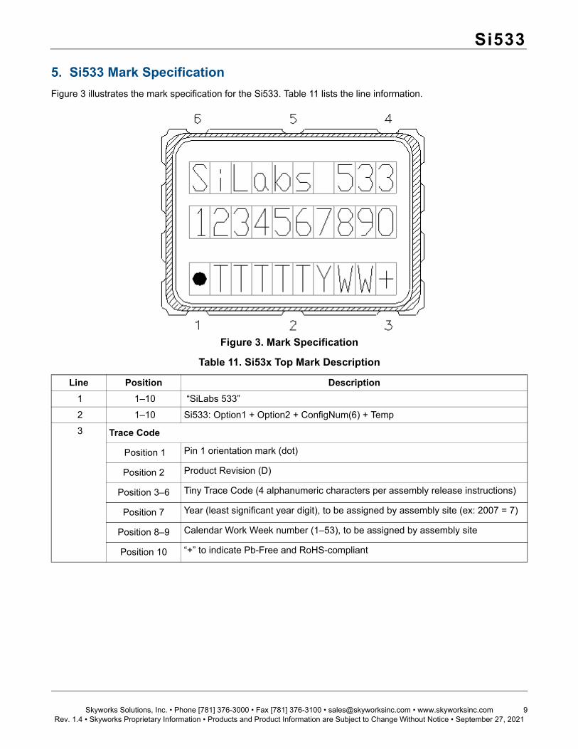
5. Si533 Mark Specification
Figure 3 illustrates the mark specification for the Si533. Table 11 lists the line information.
Figure 3. Mark Specification
Table 11. Si53x Top Mark Description
Line Position Description
1 1–10 “SiLabs 533”
2 1–10 Si533: Option1 + Option2 + ConfigNum(6) + Temp
3 Trace Code
Position 1 Pin 1 orientation mark (dot)
Position 2 Product Revision (D)
Position 3–6 Tiny Trace Code (4 alphanumeric characters per assembly release instructions)
Position 7 Year (least significant year digit), to be assigned by assembly site (ex: 2007 = 7)
Position 8–9 Calendar Work Week number (1–53), to be assigned by assembly site
Position 10 “+” to indicate Pb-Free and RoHS-compliant
Si533
10 Skyworks Solutions, Inc. • Phone [781] 376-3000 • Fax [781] 376-3100 • [email protected] • www.skyworksinc.comRev. 1.4 • Skyworks Proprietary Information • Products and Product Information are Subject to Change Without Notice • September 27, 2021
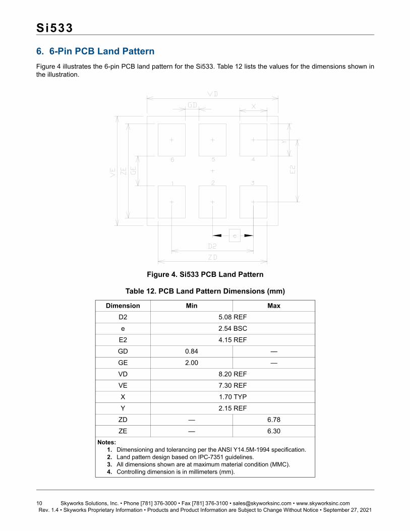
6. 6-Pin PCB Land Pattern
Figure 4 illustrates the 6-pin PCB land pattern for the Si533. Table 12 lists the values for the dimensions shown inthe illustration.
Figure 4. Si533 PCB Land Pattern
Table 12. PCB Land Pattern Dimensions (mm)
Dimension Min Max
D2 5.08 REF
e 2.54 BSC
E2 4.15 REF
GD 0.84 —
GE 2.00 —
VD 8.20 REF
VE 7.30 REF
X 1.70 TYP
Y 2.15 REF
ZD — 6.78
ZE — 6.30
Notes:1. Dimensioning and tolerancing per the ANSI Y14.5M-1994 specification.2. Land pattern design based on IPC-7351 guidelines.3. All dimensions shown are at maximum material condition (MMC).4. Controlling dimension is in millimeters (mm).
Si533
Skyworks Solutions, Inc. • Phone [781] 376-3000 • Fax [781] 376-3100 • [email protected] • www.skyworksinc.com 11Rev. 1.4 • Skyworks Proprietary Information • Products and Product Information are Subject to Change Without Notice • September 27, 2021
DOCUMENT CHANGE LIST
Revision 1.0 to Revision 1.1 Updated Table 1, “Recommended Operating
Conditions,” on page 2. Device maintains stable operation over –40 to +85 ºC
operating temperature range. Supply current specifications updated for revision D.
Updated Table 2, “CLK± Output Frequency Characteristics,” on page 2. Added specification for ±20 ppm lifetime stability
(±7 ppm temperature stability) XO.
Updated Table 3, “CLK± Output Levels and Symmetry,” on page 3. Updated LVDS differential peak-peak swing
specifications.
Updated Table 4, “CLK± Output Phase Jitter,” on page 4.
Updated Table 5, “CLK± Output Period Jitter,” on page 4.Revised period jitter specifications.
Updated Table 9, “Absolute Maximum Ratings1,” on page 5 to reflect the soldering temperature time at 260 ºC is 20–40 sec per JEDEC J-STD-020C.
Updated 3. "Ordering Information" on page 7.Changed ordering instructions to revision D.
Added 5. "Si533 Mark Specification" on page 9.
Revision 1.1 to Revision 1.2 Updated 2.5 V/3.3 V and 1.8 V CML output level
specifications for Table 3 on page 3.
Added footnotes clarifying max offset frequency test conditions for Table 4 on page 4.
Removed the words "Differential Modes: LVPECL/LVDS/CML" in the footnote referring to AN256 in Table 4 on page 4.
Added CMOS phase jitter specs to Table 4 on page 4.
Updated Table 7 on page 5 to include the "Moisture Sensitivity Level" and "Contact Pads" rows.
Revised Figure 2 on page 8 to reflect current package outline diagram.
Updated Figure 3 and Table 11 on page 9 to reflect specific marking information. Previously, Figure 3 was generic.
Updated contact information on page 12.
Revision 1.2 to Revision 1.3 Added Table 8, “Thermal Characteristics,” on
page 5.
Revision 1.3 to Revision 1.4June, 2018
Changed “Trays” to “Coil Tape” in section 3. “Ordering Information”.

Copyright © 2021 Skyworks Solutions, Inc. All Rights Reserved.Information in this document is provided in connection with Skyworks Solutions, Inc. (“Skyworks”) products or services. These materials, including the information contained herein, are provided by Skyworks as a service to its customers and may be used for informational purposes only by the customer. Skyworks assumes no responsibility for errors or omissions in these materials or the information contained herein. Skyworks may change its documentation, products, services, specifications or product descriptions at any time, without notice. Skyworks makes no commitment to update the materials or information and shall have no responsibility whatsoever for conflicts, incompatibilities, or other difficulties arising from any future changes.
No license, whether express, implied, by estoppel or otherwise, is granted to any intellectual property rights by this document. Skyworks assumes no liability for any materials, products or information provided hereunder, including the sale, distribution, reproduction or use of Skyworks products, information or materials, except as may be provided in Skyworks’ Terms and Conditions of Sale.
THE MATERIALS, PRODUCTS AND INFORMATION ARE PROVIDED “AS IS” WITHOUT WARRANTY OF ANY KIND, WHETHER EXPRESS, IMPLIED, STATUTORY, OR OTHERWISE, INCLUDING FITNESS FOR A PARTICULAR PURPOSE OR USE, MERCHANTABILITY, PERFORMANCE, QUALITY OR NON-INFRINGEMENT OF ANY INTELLECTUAL PROPERTY RIGHT; ALL SUCH WARRANTIES ARE HEREBY EXPRESSLY DISCLAIMED. SKYWORKS DOES NOT WARRANT THE ACCURACY OR COMPLETENESS OF THE INFORMATION, TEXT, GRAPHICS OR OTHER ITEMS CONTAINED WITHIN THESE MATERIALS. SKYWORKS SHALL NOT BE LIABLE FOR ANY DAMAGES, INCLUDING BUT NOT LIMITED TO ANY SPECIAL, INDIRECT, INCIDENTAL, STATUTORY, OR CONSEQUENTIAL DAMAGES, INCLUDING WITHOUT LIMITATION, LOST REVENUES OR LOST PROFITS THAT MAY RESULT FROM THE USE OF THE MATERIALS OR INFORMATION, WHETHER OR NOT THE RECIPIENT OF MATERIALS HAS BEEN ADVISED OF THE POSSIBILITY OF SUCH DAMAGE.
Skyworks products are not intended for use in medical, lifesaving or life-sustaining applications, or other equipment in which the failure of the Skyworks products could lead to personal injury, death, physical or environmental damage. Skyworks customers using or selling Skyworks products for use in such applications do so at their own risk and agree to fully indemnify Skyworks for any damages resulting from such improper use or sale.
Customers are responsible for their products and applications using Skyworks products, which may deviate from published specifications as a result of design defects, errors, or operation of products outside of published parameters or design specifications. Customers should include design and operating safeguards to minimize these and other risks. Skyworks assumes no liability for applications assistance, customer product design, or damage to any equipment resulting from the use of Skyworks products outside of Skyworks’ published specifications or parameters.
Skyworks, the Skyworks symbol, Sky5®, SkyOne®, SkyBlue™, Skyworks Green™, Clockbuilder®, DSPLL®, ISOmodem®, ProSLIC®, and SiPHY® are trademarks or registered trademarks of Skyworks Solutions, Inc. or its subsidiaries in the United States and other countries. Third-party brands and names are for identification purposes only and are the property of their respective owners. Additional information, including relevant terms and conditions, posted at www.skyworksinc.com, are incorporated by reference.
Portfoliowww.skyworksinc.com/ia/timing
SW/HWwww.skyworksinc.com/CBPro
Qualitywww.skyworksinc.com/quality
Support & Resourceswww.skyworksinc.com/support
ClockBuilder ProCustomize Skyworks clock generators, jitter attenuators and network synchronizers with a single tool. With CBPro you can control evaluation boards, access documentation, request a custom part number, export for in-system programming and more!
www.skyworksinc.com/CBPro
Skyworks Solutions, Inc. | Nasdaq: SWKS | [email protected] | www.skyworksinc.comUSA: 781-376-3000 | Asia: 886-2-2735 0399 | Europe: 33 (0)1 43548540 |