Embed Size (px)
Citation preview
Skyworks Solutions, Inc. • Phone [781] 376-3000 • Fax [781] 376-3100 • [email protected] • www.skyworksinc.comRev. 1.1 • Skyworks Proprietary Information • Products and Product Information are Subject to Change Without Notice • August 6, 2021
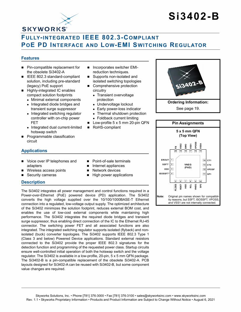
Si3402-B
FULLY- INTEGRATED IEEE 802.3-COMPLIANT POE PD INTERFACE AND LOW-EMI SWITCHING REGULATOR
Features
Applications
Description
The Si3402 integrates all power management and control functions required in aPower-over-Ethernet (PoE) powered device (PD) application. The Si3402converts the high voltage supplied over the 10/100/1000BASE-T Ethernetconnection into a regulated, low-voltage output supply. The optimized architectureof the Si3402 minimizes the solution footprint, reduces external BOM cost, andenables the use of low-cost external components while maintaining highperformance. The Si3402 integrates the required diode bridges and transientsurge suppressor, thus enabling direct connection of the IC to the Ethernet RJ-45connector. The switching power FET and all associated functions are alsointegrated. The integrated switching regulator supports isolated (flyback) and non-isolated (buck) converter topologies. The Si3402 supports IEEE 802.3 Type 1(Class 3 and below) Powered Device applications. Standard external resistorsconnected to the Si3402 provide the proper IEEE 802.3 signatures for thedetection function and programming of the requested power class. Startup circuitsensure well-controlled initial operation of both the hotswap switch and the voltageregulator. The Si3402 is available in a low-profile, 20-pin, 5 x 5 mm QFN package.The Si3402-B is a pin-compatible replacement of the obsolete Si3402-A. PCBlayouts designed for Si3402-A can be reused with Si3402-B, but some componentvalue changes are required.
Pin-compatible replacement for the obsolete Si3402-A
IEEE 802.3 standard-compliant solution, including pre-standard (legacy) PoE support
Highly-integrated IC enables compact solution footprintsMinimal external componentsIntegrated diode bridges and
transient surge suppressorIntegrated switching regulator
controller with on-chip power FET
Integrated dual current-limited hotswap switch
Programmable classification circuit
Incorporates switcher EMI-reduction techniques.
Supports non-isolated and isolated switching topologies
Comprehensive protection circuitryTransient overvoltage
protectionUndervoltage lockoutEarly power-loss indicatorThermal shutdown protectionFoldback current limiting
Low-profile 5 x 5 mm 20-pin QFN RoHS-compliant
Voice over IP telephones and adapters
Wireless access points Security cameras
Point-of-sale terminals Internet appliances Network devices High power applications
Ordering Information:See page 19.
Pin Assignments
5 x 5 mm QFN(Top View)
Note: Original pin names shown for compatibil-ity reasons, but SSFT, ISOSSFT, VPOSS,and VSS1 are not internally connected.
EROUT
SSFT*
RD
ET
HS
O
RC
L
SP1
SP
2
VPOSF
CT1
PL
OS
SISOSSFT*
VDD
5 6 7 8 9 10
1
2
3
4 11
12
13
14
VN
EG
VS
SA
VP
OS
S
VS
S1
SW
O
VS
S2
FB
VNEG(PAD)
CT2
151620 19 18 17
Si3402-B
2 Skyworks Solutions, Inc. • Phone [781] 376-3000 • Fax [781] 376-3100 • [email protected] • www.skyworksinc.comRev. 1.1 • Skyworks Proprietary Information • Products and Product Information are Subject to Change Without Notice • August 6, 2021
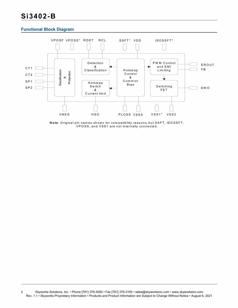
Functional Block Diagram
D e tec tio n&
C la ss ific a t io n
H o tsw a pS w itc h
&C u rre n t lim it
H o tsw a pC o n tro l
&C o m m on
B ia s
P W M C o n tro l a n d E M I L im itin g
S w itch in gF E T
Rec
tific
atio
n&
Prot
ectio
nC T 1
C T 2
S P 1
S P 2
V P O S F
V N E G
R D E T R C L
H S O
V D D
P L O S S V S S 1 *
S W O
E R O U TF B
S S F T * IS O S S F T *
V S S 2
V P O S S *
V S S A
N o te : O r ig in a l p in n a m e s sh o w n fo r co m p a tib i lity re as o n s, b u t S S F T , IS O S S F T , V P O S S , a n d V S S 1 a re n o t in te rn a lly co n n e c te d.
Si3402-B
Skyworks Solutions, Inc. • Phone [781] 376-3000 • Fax [781] 376-3100 • [email protected] • www.skyworksinc.com 3Rev. 1.1 • Skyworks Proprietary Information • Products and Product Information are Subject to Change Without Notice • August 6, 2021
TABLE OF CONTENTS
Section Page1. Electrical Specifications . . . . . . . . . . . . . . . . . . . . . . . . . . . . . . . . . . . . . . . . . . . . . . . . . . .42. Typical Application Schematics* . . . . . . . . . . . . . . . . . . . . . . . . . . . . . . . . . . . . . . . . . . . .73. Functional Description . . . . . . . . . . . . . . . . . . . . . . . . . . . . . . . . . . . . . . . . . . . . . . . . . . . .8
3.1. Overview . . . . . . . . . . . . . . . . . . . . . . . . . . . . . . . . . . . . . . . . . . . . . . . . . . . . . . . . . . .83.2. PD Hotswap Controller . . . . . . . . . . . . . . . . . . . . . . . . . . . . . . . . . . . . . . . . . . . . . . . .93.3. Isolated and Non-Isolated Application Topologies . . . . . . . . . . . . . . . . . . . . . . . . . .133.4. Switching Regulator . . . . . . . . . . . . . . . . . . . . . . . . . . . . . . . . . . . . . . . . . . . . . . . . .143.5. Output Voltage and Thermal Considerations . . . . . . . . . . . . . . . . . . . . . . . . . . . . . .15
4. Pin Descriptions . . . . . . . . . . . . . . . . . . . . . . . . . . . . . . . . . . . . . . . . . . . . . . . . . . . . . . . . .165. Package Outline . . . . . . . . . . . . . . . . . . . . . . . . . . . . . . . . . . . . . . . . . . . . . . . . . . . . . . . . .176. Recommended Land Pattern . . . . . . . . . . . . . . . . . . . . . . . . . . . . . . . . . . . . . . . . . . . . . . .187. Ordering Guide . . . . . . . . . . . . . . . . . . . . . . . . . . . . . . . . . . . . . . . . . . . . . . . . . . . . . . . . . .198. Device Marking Diagram . . . . . . . . . . . . . . . . . . . . . . . . . . . . . . . . . . . . . . . . . . . . . . . . . .20Document Change List . . . . . . . . . . . . . . . . . . . . . . . . . . . . . . . . . . . . . . . . . . . . . . . . . . . . .21
Si3402-B
4 Skyworks Solutions, Inc. • Phone [781] 376-3000 • Fax [781] 376-3100 • [email protected] • www.skyworksinc.comRev. 1.1 • Skyworks Proprietary Information • Products and Product Information are Subject to Change Without Notice • August 6, 2021
1. Electrical Specifications
Table 1. Recommended Operating Conditions
Description Symbol Min Typ Max Units
|CT1 – CT2| or |SP1 – SP2| VPORT 2.8 — 57 V
Ambient Operating Temperature TA –40 25 85 °C
Note: Unless otherwise noted, all voltages referenced to VNEG. All minimum and maximum specifications are guaranteed and apply across the recommended operating conditions. Typical values apply at nominal supply voltage and ambient temperature unless otherwise noted.
Table 2. Absolute Maximum Ratings1
Type Description Rating Unit
Voltage
CT1 to CT22 –100 to 100
V
SP1 to SP22 –100 to 100
VPOS –0.7 to 100
HSO –0.7 to 100
VSS1, VSS2, or VSSA –0.7 to 100
VSS1 to VSS2 or VSSA –0.3 to 0.3
SWO3 –0.7 to 100
PLOSS to VPOS –100 to 0.7
RDET –0.7 to 100
VDD to VSS1, VSS2, or VSSA –0.3 to 5.5
Peak CurrentCT1, CT2, SP1, SP22 –5 to 5
AVPOS2 –5 to 5
DC Current4 CT1,CT2,SP1,SP2 –0.2 to 0.2 A
Ambient TemperatureStorage –65 to 150
°COperating –40 to 85
Notes:1. Unless otherwise noted, all voltages referenced to VNEG. Permanent device damage may occur if the maximum ratings
are exceeded. Functional operation should be restricted to those conditions specified in the operational sections of this data sheet. Exposure to absolute maximum rating conditions for extended periods may adversely affect device reliability.
2. Si3402 provides internal protection from certain transient surge voltages on these pins. Please refer to “AN956: Si3402-B POE PD Controller Design Guide” for details.
3. SWO is referenced to VSS2.4. Higher dc current is possible in the application, but only utilizing external bridge diodes. Refer to “AN956: Si3402-B-
POE-PD Controller Design Guide” for more information.
Si3402-B
Skyworks Solutions, Inc. • Phone [781] 376-3000 • Fax [781] 376-3100 • [email protected] • www.skyworksinc.com 5Rev. 1.1 • Skyworks Proprietary Information • Products and Product Information are Subject to Change Without Notice • August 6, 2021
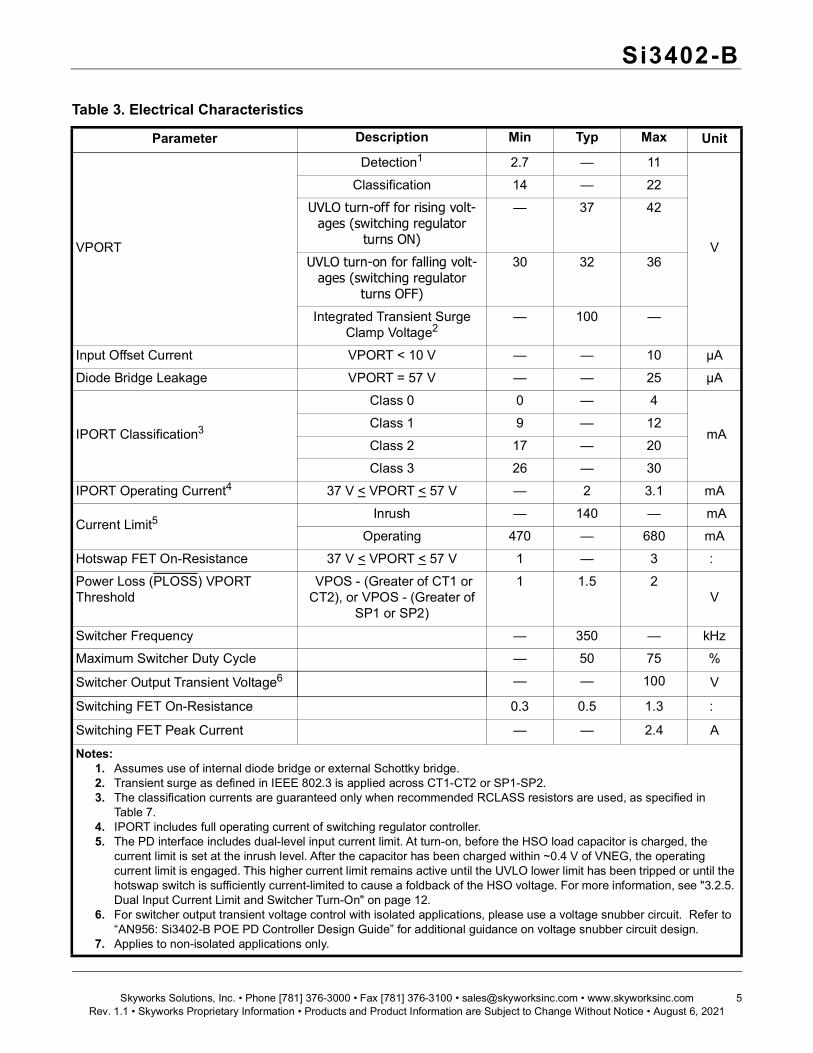
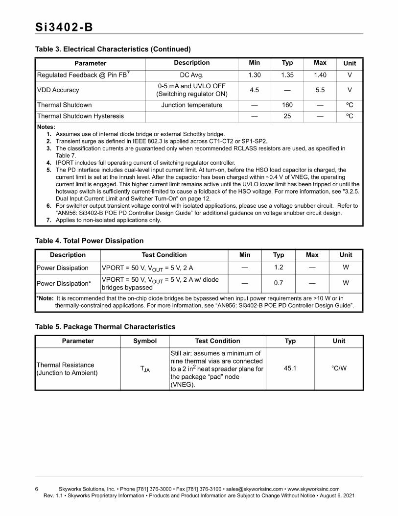
Table 3. Electrical Characteristics
Parameter Description Min Typ Max Unit
VPORT
Detection1 2.7 — 11
V
Classification 14 — 22UVLO turn-off for rising volt-
ages (switching regulator turns ON)
— 37 42
UVLO turn-on for falling volt-ages (switching regulator
turns OFF)
30 32 36
Integrated Transient Surge Clamp Voltage2
— 100 —
Input Offset Current VPORT < 10 V — — 10 µADiode Bridge Leakage VPORT = 57 V — — 25 µA
IPORT Classification3
Class 0 0 — 4
mAClass 1 9 — 12Class 2 17 — 20Class 3 26 — 30
IPORT Operating Current4 37 V < VPORT < 57 V — 2 3.1 mA
Current Limit5Inrush — 140 — mA
Operating 470 — 680 mAHotswap FET On-Resistance 37 V < VPORT < 57 V 1 — 3
Power Loss (PLOSS) VPORT Threshold
VPOS - (Greater of CT1 or CT2), or VPOS - (Greater of
SP1 or SP2)
1 1.5 2V
Switcher Frequency — 350 — kHzMaximum Switcher Duty Cycle — 50 75 %
Switcher Output Transient Voltage6 — — 100 V
Switching FET On-Resistance 0.3 0.5 1.3
Switching FET Peak Current — — 2.4 A
Notes:1. Assumes use of internal diode bridge or external Schottky bridge.2. Transient surge as defined in IEEE 802.3 is applied across CT1-CT2 or SP1-SP2.3. The classification currents are guaranteed only when recommended RCLASS resistors are used, as specified in
Table 7.4. IPORT includes full operating current of switching regulator controller.5. The PD interface includes dual-level input current limit. At turn-on, before the HSO load capacitor is charged, the
current limit is set at the inrush level. After the capacitor has been charged within ~0.4 V of VNEG, the operating current limit is engaged. This higher current limit remains active until the UVLO lower limit has been tripped or until the hotswap switch is sufficiently current-limited to cause a foldback of the HSO voltage. For more information, see "3.2.5. Dual Input Current Limit and Switcher Turn-On" on page 12.
6. For switcher output transient voltage control with isolated applications, please use a voltage snubber circuit. Refer to “AN956: Si3402-B POE PD Controller Design Guide” for additional guidance on voltage snubber circuit design.
7. Applies to non-isolated applications only.
Si3402-B
6 Skyworks Solutions, Inc. • Phone [781] 376-3000 • Fax [781] 376-3100 • [email protected] • www.skyworksinc.comRev. 1.1 • Skyworks Proprietary Information • Products and Product Information are Subject to Change Without Notice • August 6, 2021
Regulated Feedback @ Pin FB7 DC Avg. 1.30 1.35 1.40 V
VDD Accuracy 0-5 mA and UVLO OFF (Switching regulator ON) 4.5 — 5.5 V
Thermal Shutdown Junction temperature — 160 — ºCThermal Shutdown Hysteresis — 25 — ºC
Table 4. Total Power Dissipation
Description Test Condition Min Typ Max Unit
Power Dissipation VPORT = 50 V, VOUT = 5 V, 2 A — 1.2 — W
Power Dissipation* VPORT = 50 V, VOUT = 5 V, 2 A w/ diode bridges bypassed
— 0.7 — W
*Note: It is recommended that the on-chip diode bridges be bypassed when input power requirements are >10 W or in thermally-constrained applications. For more information, see “AN956: Si3402-B POE PD Controller Design Guide”.
Table 5. Package Thermal Characteristics
Parameter Symbol Test Condition Typ Unit
Thermal Resistance(Junction to Ambient)
JA
Still air; assumes a minimum of nine thermal vias are connected to a 2 in2 heat spreader plane for the package “pad” node (VNEG).
45.1 °C/W
Table 3. Electrical Characteristics (Continued)
Parameter Description Min Typ Max Unit
Notes:1. Assumes use of internal diode bridge or external Schottky bridge.2. Transient surge as defined in IEEE 802.3 is applied across CT1-CT2 or SP1-SP2.3. The classification currents are guaranteed only when recommended RCLASS resistors are used, as specified in
Table 7.4. IPORT includes full operating current of switching regulator controller.5. The PD interface includes dual-level input current limit. At turn-on, before the HSO load capacitor is charged, the
current limit is set at the inrush level. After the capacitor has been charged within ~0.4 V of VNEG, the operating current limit is engaged. This higher current limit remains active until the UVLO lower limit has been tripped or until the hotswap switch is sufficiently current-limited to cause a foldback of the HSO voltage. For more information, see "3.2.5. Dual Input Current Limit and Switcher Turn-On" on page 12.
6. For switcher output transient voltage control with isolated applications, please use a voltage snubber circuit. Refer to “AN956: Si3402-B POE PD Controller Design Guide” for additional guidance on voltage snubber circuit design.
7. Applies to non-isolated applications only.
Si3402-B
Skyworks Solutions, Inc. • Phone [781] 376-3000 • Fax [781] 376-3100 • [email protected] • www.skyworksinc.com 7Rev. 1.1 • Skyworks Proprietary Information • Products and Product Information are Subject to Change Without Notice • August 6, 2021
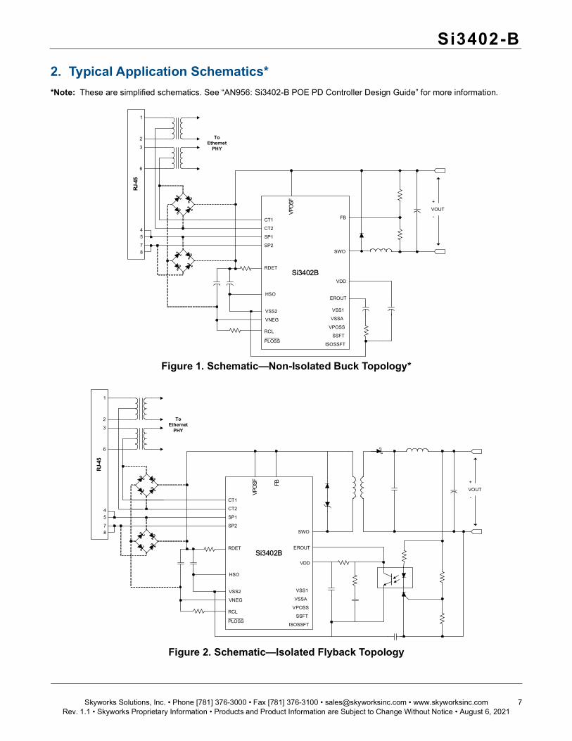
2. Typical Application Schematics**Note: These are simplified schematics. See “AN956: Si3402-B POE PD Controller Design Guide” for more information.
Figure 1. Schematic—Non-Isolated Buck Topology*
Figure 2. Schematic—Isolated Flyback Topology
Si3402B
RCL
RDET
CT1
CT2
SP1
SP2
VPOS
F
SSFT
VDD
ISOSSFT
VPOSSVNEG
HSO
VSS1
PLOSS
VSS2VSSA
SWO
FB
EROUT
RJ-
45
VOUT+
-
1
2
3
4
5
6
7
8
To Ethernet
PHY
Si3402B
RCL
RDET
CT1
CT2
SP1
SP2
VPOS
F
SSFT
VDD
ISOSSFT
VPOSSVNEG
HSO
VSS1
PLOSS
VSS2VSSA
SWO
FB
EROUT
VOUT+
-
RJ-
45
1
2
3
4
5
6
7
8
To Ethernet
PHY
Si3402-B
8 Skyworks Solutions, Inc. • Phone [781] 376-3000 • Fax [781] 376-3100 • [email protected] • www.skyworksinc.comRev. 1.1 • Skyworks Proprietary Information • Products and Product Information are Subject to Change Without Notice • August 6, 2021
3. Functional DescriptionThe Si3402 consists of two major functions: a hotswap controller/interface and a complete pulse-width-modulatedswitching regulator (controller and power FET).
3.1. OverviewThe hotswap interface of the Si3402 provides the complete front end of an IEEE 802.3-compliant PD. The Si3402also includes two full diode bridges, a transient voltage surge suppressor, detection circuit, classification currentsource, and dual-level hotswap current limiting switch. This high level of integration enables direct connection tothe RJ-45 connector, simplifies system design, and provides significant advantages for reliability and protection.The Si3402 requires only four standard external components (detection resistor, optional classification resistor,load capacitor, and input capacitor) to create a fully IEEE 802.3-compliant interface.The Si3402 integrates a complete pulse-width modulated switching regulator that includes the controller and powerFET. The switching regulator utilizes a constant frequency pulse-width modulated controller optimized for allpossible load conditions in PoE applications. The regulator integrates a low on-resistance (Ron) switching powerMOSFET that minimizes power dissipation, increases overall regulator efficiency, and simplifies system design. Anintegrated error amplifier, precision reference, and soft-start feature provide the flexibility of using a non-isolatedbuck regulator topology or an isolated flyback regulator topology.The Si3402 is designed to operate with both IEEE 802.3-compliant Power Sourcing Equipment (PSE) and pre-standard (legacy) PSEs that do not adhere to the IEEE 802.3 specified inrush current limits. The Si3402 iscompatible with compliant and legacy PSEs because it uses two levels for the hotswap current limits. By setting theinitial inrush current limit to a low level, a PD based on the Si3402 minimizes the current drawn from either acompliant or legacy PSE during startup. After powering up, the Si3402 automatically switches to a higher-levelcurrent limit, thereby allowing the PD to consume up to 12.95 W (the max power allowed by the IEEE 802.3specification).Excessive power cycling or short circuit faults will engage the thermal overload protection to prevent the on-chippower MOSFETs from exceeding their safe and reliable operating ranges. The switching regulator power MOSFEThas been designed and sized to withstand the high peak currents created when converting a high-voltage, low-current supply into a low-voltage, high-current supply.
Si3402-B
Skyworks Solutions, Inc. • Phone [781] 376-3000 • Fax [781] 376-3100 • [email protected] • www.skyworksinc.com 9Rev. 1.1 • Skyworks Proprietary Information • Products and Product Information are Subject to Change Without Notice • August 6, 2021
3.2. PD Hotswap ControllerThe Si3402 hotswap controller changes its mode of operation based on the input voltage applied to the high-voltage supply inputs (CT1, CT2, SP1, SP2), the IEEE 802.3-defined modes of operation, and internal controllerrequirements. Table 6 defines the modes of operation for the hotswap interface.
Figure 3 provides a representation of the input lines, protection, and hotswap circuits on the Si3402.
Figure 3. Input Lineside and Hotswap Block Diagram
Table 6. Hotswap Interface ModesInput Voltage
(|CT1-CT2| or |SP1-SP2|)Si3402 Mode
0 to 2.7 V Inactive2.7 to 11 V Detection signature11 to 14 V Transition region14 to 22 V Classification signature22 to 42 V Transition region
37 up to 57 V Switcher operating mode (hysteresis limit based on rising input voltage)
57 down to 32 V Switcher operating mode (hysteresis limit based on falling input voltage)
DIODE BRIDGESAND PROTECTION
DETECTIONCONTROL
ON
OFF
VPOS
VNEG
CT1/SP1
CT2/SP2
~2.7V
RDET
CLASSIFICATIONCONTROL
ON
OFF
RCL
CENTRAL BIASBANDGAP REF
CURRENTLIMIT
HI/LO
HOTSWAPCONTROL
ON
OFF
~37V (rising)
~32V (falling)
SWITCHER STARTUP & BIAS
HSO
POWER LOSS DETECTOR
______PLOSS
BIAS VOLTAGES
~11V
~14V
~22V
Si3402-B
10 Skyworks Solutions, Inc. • Phone [781] 376-3000 • Fax [781] 376-3100 • [email protected] • www.skyworksinc.comRev. 1.1 • Skyworks Proprietary Information • Products and Product Information are Subject to Change Without Notice • August 6, 2021
3.2.1. Rectification Diode Bridges and Surge SuppressorThe IEEE 802.3 specification defines the input voltage at the RJ-45 connector of the PD with no reference topolarity. In other words, the PD must be able to accept power of either polarity at each of its inputs. Thisrequirement necessitates the use of two sets of diode bridges, one for the CT1 and CT2 pins and one for the SP1and SP2 pins to rectify the voltage. Furthermore, the standard requires that a PD withstand a high-voltage transientsurge as defined in the IEEE 802.3 specification. Typically, the diode bridge and the surge suppressor have beenimplemented externally, adding cost and complexity to the PD system design.The diode bridge* and the surge suppressor have been integrated into the Si3402, thus reducing system cost anddesign complexity.*Note: It is recommended that the on-chip diode bridges be bypassed when input power requirements are >10 W or in
thermally-constrained applications. For more information, see “AN956: Si3402-B POE PD Controller Design Guide”.By integrating the diode bridges, the Si3402 gains access to the input side of the diode bridge. Monitoring thevoltage at the input of the diode bridges instead of the voltage across the load capacitor provides the earliestindication of a power loss. This true early power loss indicator, PLOSS, provides the PD’s processor a bit of time tosave states and shut down gracefully before the load capacitor discharges below the minimum IEEE 802.3-specified operating voltage of 36 V. Integration of the surge suppressor enables optimization of the clampingvoltage and guarantees protection of all connected circuitry.As an added benefit, the transient surge suppressor, when tripped, actively disables the hotswap interface andswitching regulator, preventing downstream circuits from encountering the high-energy transients.3.2.2. DetectionIn order to identify a device as a valid PD, a PSE will apply a voltage in the range of 2.8 to 10 V on the cable andlook for a valid signature resistance. The Si3402 will react to voltages in this range by connecting the external24.3 k detection resistor between VPOS and VNEG. This external resistor and internal low-leakage controlcircuitry create the proper signature to alert the PSE that a valid PD has been detected and is ready to have powerapplied. The internal hotswap switch is disabled during this time to prevent the switching regulator and attachedload circuitry from generating errors in the detection signature.Since the Si3402 integrates the diode bridges, the IC can compensate for the voltage and resistance effects of thediode bridges. The IEEE 802.3 specification requires that the PSE use a multi-point, V/I measurement techniqueto remove the diode-induced dc offset from the signature resistance measurement. However, the specificationdoes not address the diode's nonlinear resistance and the error induced in the signature resistor measurement.Since the diode's resistance appears in series with the signature resistor, the PD system must find some way ofcompensating for this error. In systems where the diode bridges are external, compensation is difficult and suffersfrom errors. Since the diode bridges are integrated in the Si3402, the IC can compensate for this error by offsettingresistance across all operating conditions and thus meeting the IEEE 802.3 requirements.
Si3402-B
Skyworks Solutions, Inc. • Phone [781] 376-3000 • Fax [781] 376-3100 • [email protected] • www.skyworksinc.com 11Rev. 1.1 • Skyworks Proprietary Information • Products and Product Information are Subject to Change Without Notice • August 6, 2021
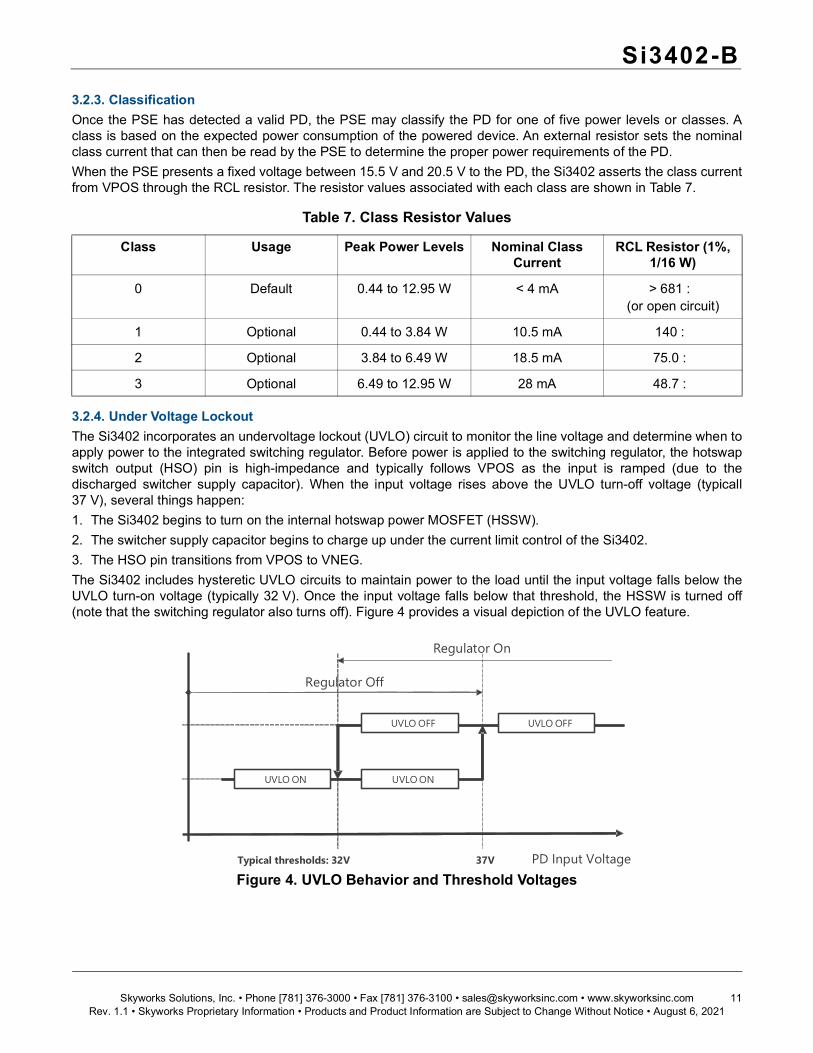
3.2.3. ClassificationOnce the PSE has detected a valid PD, the PSE may classify the PD for one of five power levels or classes. Aclass is based on the expected power consumption of the powered device. An external resistor sets the nominalclass current that can then be read by the PSE to determine the proper power requirements of the PD.When the PSE presents a fixed voltage between 15.5 V and 20.5 V to the PD, the Si3402 asserts the class currentfrom VPOS through the RCL resistor. The resistor values associated with each class are shown in Table 7.
3.2.4. Under Voltage LockoutThe Si3402 incorporates an undervoltage lockout (UVLO) circuit to monitor the line voltage and determine when toapply power to the integrated switching regulator. Before power is applied to the switching regulator, the hotswapswitch output (HSO) pin is high-impedance and typically follows VPOS as the input is ramped (due to thedischarged switcher supply capacitor). When the input voltage rises above the UVLO turn-off voltage (typicall37 V), several things happen:1. The Si3402 begins to turn on the internal hotswap power MOSFET (HSSW).2. The switcher supply capacitor begins to charge up under the current limit control of the Si3402.3. The HSO pin transitions from VPOS to VNEG.The Si3402 includes hysteretic UVLO circuits to maintain power to the load until the input voltage falls below theUVLO turn-on voltage (typically 32 V). Once the input voltage falls below that threshold, the HSSW is turned off(note that the switching regulator also turns off). Figure 4 provides a visual depiction of the UVLO feature.
Figure 4. UVLO Behavior and Threshold Voltages
Table 7. Class Resistor Values
Class Usage Peak Power Levels Nominal Class Current
RCL Resistor (1%,1/16 W)
0 Default 0.44 to 12.95 W < 4 mA > 681 (or open circuit)
1 Optional 0.44 to 3.84 W 10.5 mA 140
2 Optional 3.84 to 6.49 W 18.5 mA 75.0
3 Optional 6.49 to 12.95 W 28 mA 48.7
PD Input Voltage
Regulator Off
32V 37V
Regulator On
Typical thresholds:
UVLO ON UVLO ON
UVLO OFF UVLO OFF
Si3402-B
12 Skyworks Solutions, Inc. • Phone [781] 376-3000 • Fax [781] 376-3100 • [email protected] • www.skyworksinc.comRev. 1.1 • Skyworks Proprietary Information • Products and Product Information are Subject to Change Without Notice • August 6, 2021
3.2.5. Dual Input Current Limit and Switcher Turn-OnThe Si3402 implements dual input current limits. While the HSSW is charging the switcher supply capacitor, theSi3402 maintains a low current limit. The switching regulator is disabled until the voltage across the HSSWbecomes sufficiently low, indicating the switcher supply capacitor is almost completely charged. When thisthreshold is reached, the switcher is activated, and the hotswap current limit is increased.The Si3402 stays in the high-level input current limit mode until the input voltage drops below the UVLO turn-onthreshold or excessive power is dissipated in the hotswap switch.An additional feature of the current limit circuitry is current limiting in the event of a fault condition. When the currentlimit is switched to the higher level, 470 mA of current can be drawn by the PD. Should a fault cause more than thiscurrent to be consumed, the HSSW goes into a temporary 10 mA current limit mode and turns off the switcher.After 90 ms have elapsed, and if the switcher supply capacitor is recharged, the HSSW turns back on in the470 mA limit mode, and enables the switcher.3.2.6. Power Loss IndicatorA situation can occur in which power is lost at the input of the diode bridge and the hotswap controller does notdetect the fault due to the VPOS to VNEG capacitor maintaining the voltage. In such a situation, the PD can remainoperational for hundreds of microseconds despite the PSE having removed the line voltage. If it is recognized earlyenough, the time from power loss to power failure can provide valuable time to gracefully shut down an application.Due to integration of the diode bridges, the Si3402 is able to instantaneously detect the removal of the line voltageand provide that early warning signal to the PD application. The PLOSS pin is an open drain output that pulls up toVPOS when the voltage difference between VPOSS and CTx or SPx is smaller than 1.5 V. When VPOSS-CTx orVPOSS-SPx voltage become >1.5 V, the output becomes high-impedance, allowing an external pull-down resistorto change the logic state of PLOSS. The benefit of this indicator is that the powered device may include amicrocontroller that can quickly save its memory or operational state before draining the supply capacitors andpowering itself down. This feature can help improve overall manageability in applications, such as wireless accesspoints.
Si3402-B
Skyworks Solutions, Inc. • Phone [781] 376-3000 • Fax [781] 376-3100 • [email protected] • www.skyworksinc.com 13Rev. 1.1 • Skyworks Proprietary Information • Products and Product Information are Subject to Change Without Notice • August 6, 2021
3.3. Isolated and Non-Isolated Application TopologiesPower over Ethernet (PoE) applications fall into two broad categories, isolated and non-isolated. Non-isolatedsystems can be used when the powered device is self-contained and does not provide external conductors to theuser or another application. Non-isolated applications include wireless access points and security cameras. Inthese applications, there is no explicit need for dc isolation between the switching regulator output and the hotswapinterface. An isolated system must be used when the powered device interfaces with other self-poweredequipment or has external conductors accessible to the user or other applications. For proper operation, theregulated output supply of the switching regulator must not have a dc electrical path to the hotswap interface orswitching regulator primary side. Isolated applications include point-of-sale terminals where the user can touch thegrounded metal chassis.The application determines the converter topology. An isolated application will require a flyback transformer-basedswitching topology while a non-isolated application can use an inductor-based buck converter topology. In theisolated case, dc isolation is achieved through a transformer in the forward path and a voltage reference plus opto-isolator in the feedback path. The application circuit shown in Figure 2 is an example of such a topology. The non-isolated application in Figure 1 makes use of a single inductor as the energy conversion element, and the feedbacksignal is directly supplied into the internal error amplifier. As can be seen from the application circuits, the isolatedtopology has an increased number of components, thus increasing the bill of materials (BOM) and system footprint.To optimize cost and ease implementation, each application should be evaluated for its isolated or non-isolatedrequirements.
Si3402-B
14 Skyworks Solutions, Inc. • Phone [781] 376-3000 • Fax [781] 376-3100 • [email protected] • www.skyworksinc.comRev. 1.1 • Skyworks Proprietary Information • Products and Product Information are Subject to Change Without Notice • August 6, 2021
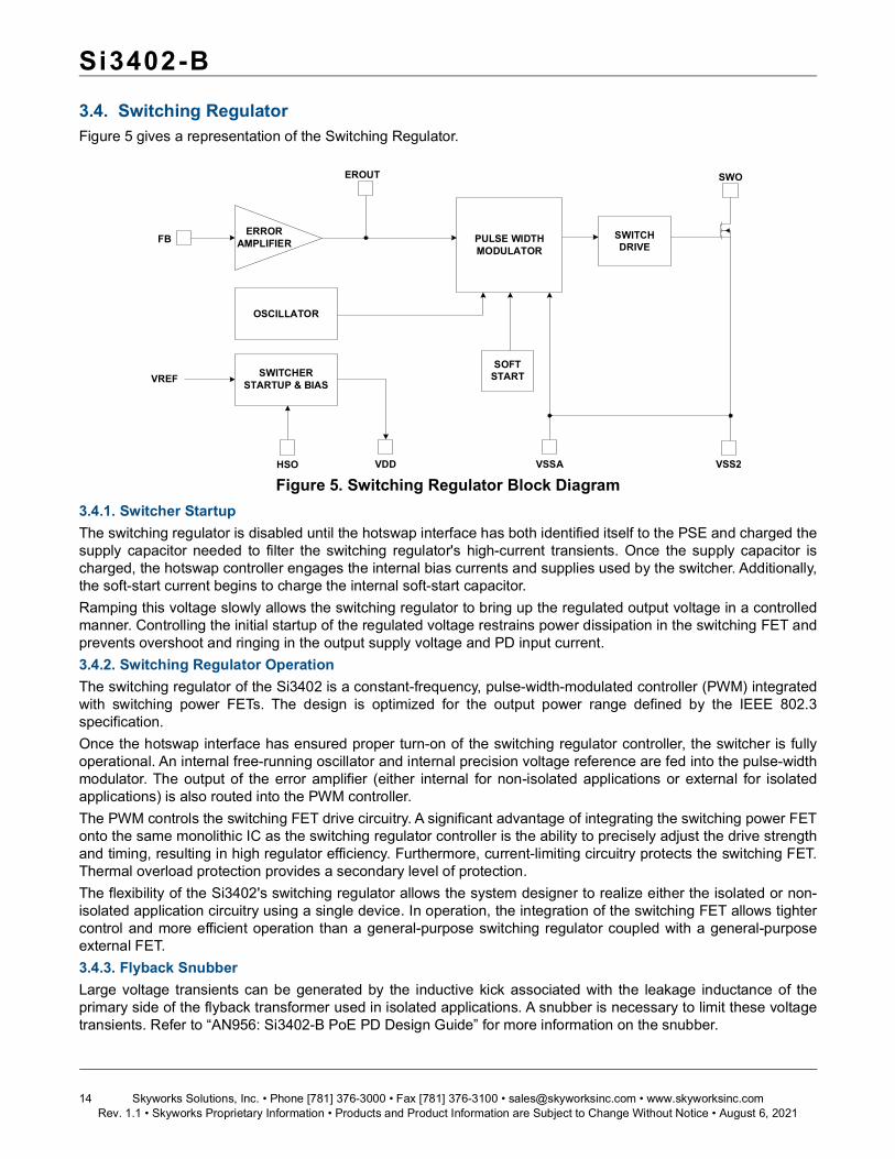
3.4. Switching RegulatorFigure 5 gives a representation of the Switching Regulator.
Figure 5. Switching Regulator Block Diagram3.4.1. Switcher StartupThe switching regulator is disabled until the hotswap interface has both identified itself to the PSE and charged thesupply capacitor needed to filter the switching regulator's high-current transients. Once the supply capacitor ischarged, the hotswap controller engages the internal bias currents and supplies used by the switcher. Additionally,the soft-start current begins to charge the internal soft-start capacitor.Ramping this voltage slowly allows the switching regulator to bring up the regulated output voltage in a controlledmanner. Controlling the initial startup of the regulated voltage restrains power dissipation in the switching FET andprevents overshoot and ringing in the output supply voltage and PD input current.3.4.2. Switching Regulator OperationThe switching regulator of the Si3402 is a constant-frequency, pulse-width-modulated controller (PWM) integratedwith switching power FETs. The design is optimized for the output power range defined by the IEEE 802.3specification.Once the hotswap interface has ensured proper turn-on of the switching regulator controller, the switcher is fullyoperational. An internal free-running oscillator and internal precision voltage reference are fed into the pulse-widthmodulator. The output of the error amplifier (either internal for non-isolated applications or external for isolatedapplications) is also routed into the PWM controller.The PWM controls the switching FET drive circuitry. A significant advantage of integrating the switching power FETonto the same monolithic IC as the switching regulator controller is the ability to precisely adjust the drive strengthand timing, resulting in high regulator efficiency. Furthermore, current-limiting circuitry protects the switching FET.Thermal overload protection provides a secondary level of protection.The flexibility of the Si3402's switching regulator allows the system designer to realize either the isolated or non-isolated application circuitry using a single device. In operation, the integration of the switching FET allows tightercontrol and more efficient operation than a general-purpose switching regulator coupled with a general-purposeexternal FET.3.4.3. Flyback SnubberLarge voltage transients can be generated by the inductive kick associated with the leakage inductance of theprimary side of the flyback transformer used in isolated applications. A snubber is necessary to limit these voltagetransients. Refer to “AN956: Si3402-B PoE PD Design Guide” for more information on the snubber.
SWITCHER STARTUP & BIAS
PULSE WIDTH MODULATOR
EROUT
HSO
VREF
SOFT START
SWITCH DRIVE
FBERROR
AMPLIFIER
OSCILLATOR
VDD
SWO
VSSA VSS2
Si3402-B
Skyworks Solutions, Inc. • Phone [781] 376-3000 • Fax [781] 376-3100 • [email protected] • www.skyworksinc.com 15Rev. 1.1 • Skyworks Proprietary Information • Products and Product Information are Subject to Change Without Notice • August 6, 2021
3.5. Output Voltage and Thermal ConsiderationsThe Si3402-B supports a wide range of output voltages for IEEE 802.3-compliant Class 0-3 designs. Because theSi3402-B integrates the switching FET and HSSW, the case temperature of the Si3402-B will depend heavily onthe output power and the thermal relief provided in the PCB design. For a given output power, the integratedHSSW will dissipate more power when configured for lower output voltages because the current passing through itis higher.The user should closely follow the hardware design guidelines provided in “AN956: Si3402-B PoE PD ControllerDesign Guide” to ensure a robust PoE PD solution, particularly for low output voltage Class 3 designs.
Si3402-B
16 Skyworks Solutions, Inc. • Phone [781] 376-3000 • Fax [781] 376-3100 • [email protected] • www.skyworksinc.comRev. 1.1 • Skyworks Proprietary Information • Products and Product Information are Subject to Change Without Notice • August 6, 2021
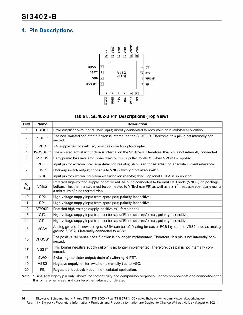
4. Pin Descriptions
Table 8. Si3402-B Pin Descriptions (Top View)Pin# Name Description
1 EROUT Error-amplifier output and PWM input; directly connected to opto-coupler in isolated application.
2 SSFT* The non-isolated soft-start function is internal on the Si3402-B. Therefore, this pin is not internally con-nected.
3 VDD 5 V supply rail for switcher; provides drive for opto-coupler.4 ISOSSFT* The isolated soft-start function is internal on the Si3402-B. Therefore, this pin is not internally connected.5 PLOSS Early power loss indicator; open drain output is pulled to VPOS when VPORT is applied.6 RDET Input pin for external precision detection resistor; also used for establishing absolute current reference.7 HSO Hotswap switch output; connects to VNEG through hotswap switch.8 RCL Input pin for external precision classification resistor; float if optional RCLASS is unused.
9, Pad VNEG
Rectified high-voltage supply, negative rail. Must be connected to thermal PAD node (VNEG) on package bottom. This thermal pad must be connected to VNEG (pin #9) as well as a 2 in2 heat spreader plane using a minimum of nine thermal vias.
10 SP2 High-voltage supply input from spare pair; polarity-insensitive.11 SP1 High-voltage supply input from spare pair; polarity-insensitive.12 VPOSF Rectified high-voltage supply, positive rail (force node)13 CT2 High-voltage supply input from center tap of Ethernet transformer; polarity-insensitive.14 CT1 High-voltage supply input from center tap of Ethernet transformer; polarity-insensitive.
15 VSSA Analog ground. In new designs, VSSA can be left floating for easier PCB layout, and VSS2 used as analog ground. VSSA is internally connected to VSS2.
16 VPOSS* The positive rail sense node function is no longer implemented. Therefore, this pin is not internally con-nected.
17 VSS1* This former negative supply rail pin is no longer implemented. Therefore, this pin is not internally con-nected.
18 SWO Switching transistor output; drain of switching N-FET.19 VSS2 Negative supply rail for switcher; externally tied to HSO.20 FB Regulated feedback input in non-isolated application.
Note: * Si3402-A legacy pin only, shown for compatibility and comparison purposes. Legacy components and connections for this pin are harmless and can be either retained or deleted.
EROUT
SSFT*
RD
ET
HS
O
RC
L
SP1
SP
2
VPOSF
CT1
PL
OS
S
ISOSSFT*
VDD
5 6 7 8 9 10
1
2
3
4 11
12
13
14
VN
EG
VS
SA
VP
OS
S
VS
S1
SW
O
VS
S2
FB
VNEG(PAD)
CT2
151620 19 18 17
Si3402-B
Skyworks Solutions, Inc. • Phone [781] 376-3000 • Fax [781] 376-3100 • [email protected] • www.skyworksinc.com 17Rev. 1.1 • Skyworks Proprietary Information • Products and Product Information are Subject to Change Without Notice • August 6, 2021
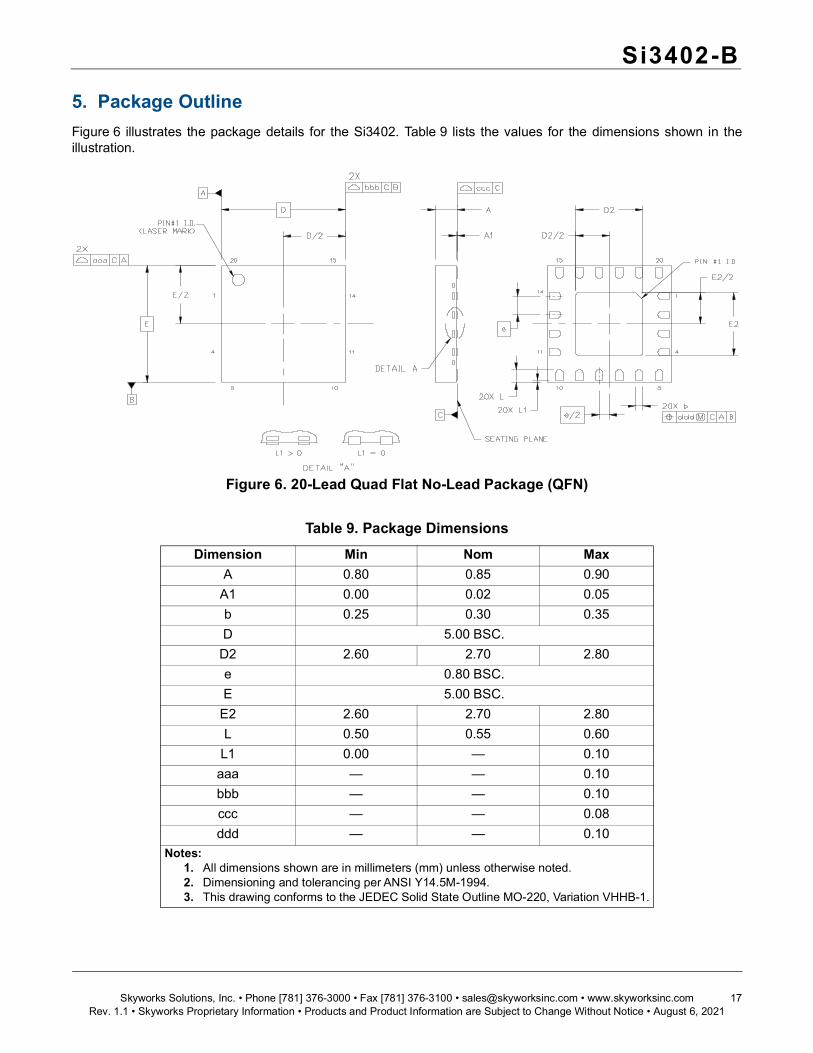
5. Package OutlineFigure 6 illustrates the package details for the Si3402. Table 9 lists the values for the dimensions shown in theillustration.
Figure 6. 20-Lead Quad Flat No-Lead Package (QFN)
Table 9. Package DimensionsDimension Min Nom Max
A 0.80 0.85 0.90A1 0.00 0.02 0.05b 0.25 0.30 0.35D 5.00 BSC.D2 2.60 2.70 2.80e 0.80 BSC.E 5.00 BSC.E2 2.60 2.70 2.80L 0.50 0.55 0.60L1 0.00 — 0.10aaa — — 0.10bbb — — 0.10ccc — — 0.08ddd — — 0.10
Notes:1. All dimensions shown are in millimeters (mm) unless otherwise noted.2. Dimensioning and tolerancing per ANSI Y14.5M-1994.3. This drawing conforms to the JEDEC Solid State Outline MO-220, Variation VHHB-1.
Si3402-B
18 Skyworks Solutions, Inc. • Phone [781] 376-3000 • Fax [781] 376-3100 • [email protected] • www.skyworksinc.comRev. 1.1 • Skyworks Proprietary Information • Products and Product Information are Subject to Change Without Notice • August 6, 2021
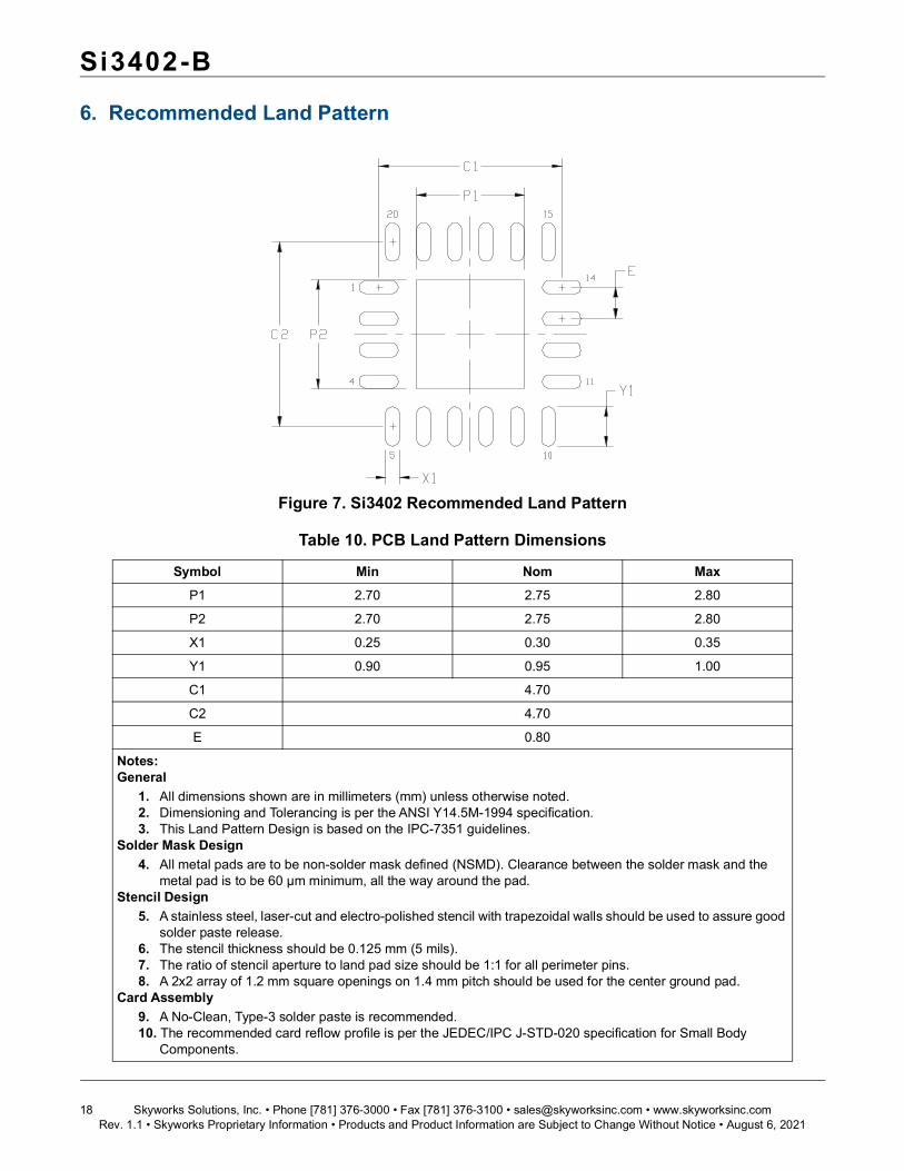
6. Recommended Land Pattern
Figure 7. Si3402 Recommended Land Pattern
Table 10. PCB Land Pattern Dimensions
Symbol Min Nom MaxP1 2.70 2.75 2.80
P2 2.70 2.75 2.80
X1 0.25 0.30 0.35
Y1 0.90 0.95 1.00
C1 4.70
C2 4.70
E 0.80
Notes:General
1. All dimensions shown are in millimeters (mm) unless otherwise noted.2. Dimensioning and Tolerancing is per the ANSI Y14.5M-1994 specification.3. This Land Pattern Design is based on the IPC-7351 guidelines.
Solder Mask Design4. All metal pads are to be non-solder mask defined (NSMD). Clearance between the solder mask and the
metal pad is to be 60 µm minimum, all the way around the pad.Stencil Design
5. A stainless steel, laser-cut and electro-polished stencil with trapezoidal walls should be used to assure good solder paste release.
6. The stencil thickness should be 0.125 mm (5 mils).7. The ratio of stencil aperture to land pad size should be 1:1 for all perimeter pins.8. A 2x2 array of 1.2 mm square openings on 1.4 mm pitch should be used for the center ground pad.
Card Assembly9. A No-Clean, Type-3 solder paste is recommended.10. The recommended card reflow profile is per the JEDEC/IPC J-STD-020 specification for Small Body
Components.
Si3402-B
Skyworks Solutions, Inc. • Phone [781] 376-3000 • Fax [781] 376-3100 • [email protected] • www.skyworksinc.com 19Rev. 1.1 • Skyworks Proprietary Information • Products and Product Information are Subject to Change Without Notice • August 6, 2021
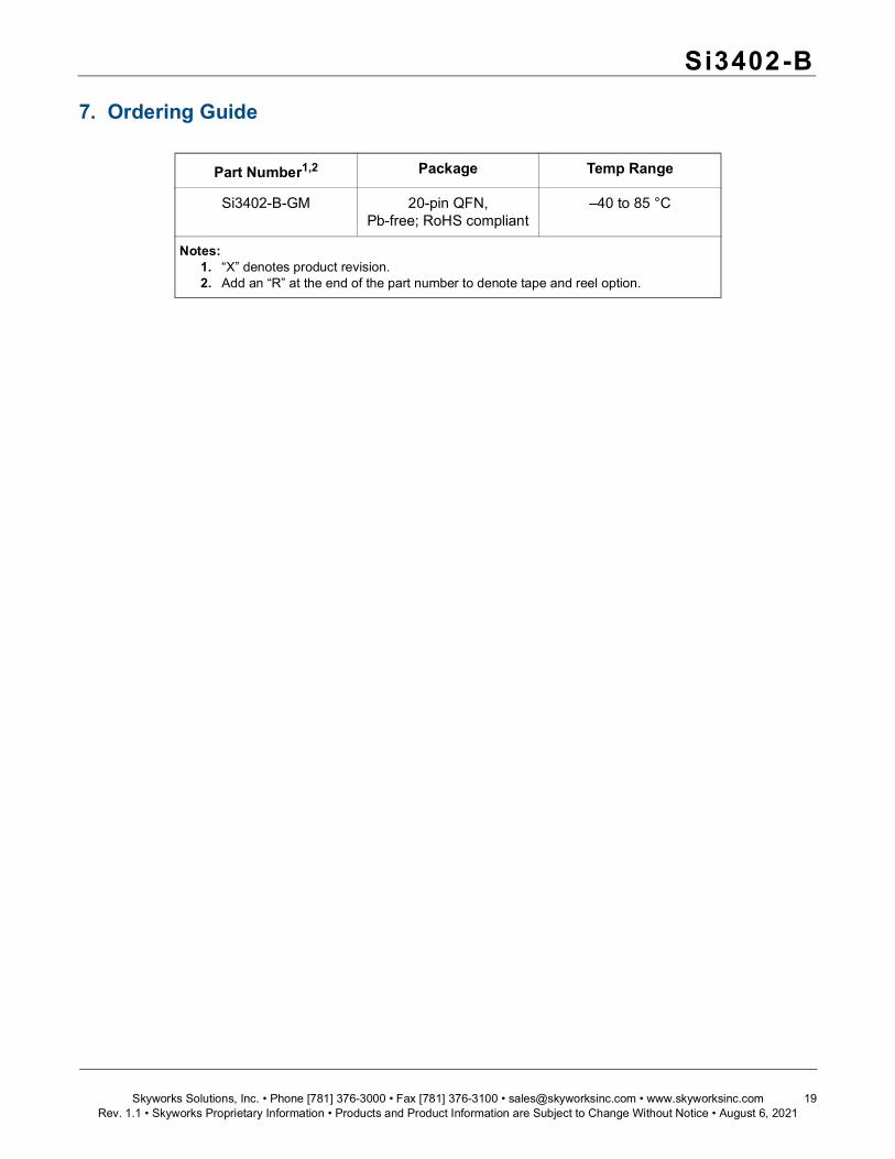
7. Ordering Guide
Part Number1,2 Package Temp Range
Si3402-B-GM 20-pin QFN,Pb-free; RoHS compliant
–40 to 85 °C
Notes:1. “X” denotes product revision.2. Add an “R” at the end of the part number to denote tape and reel option.
Si3402-B
20 Skyworks Solutions, Inc. • Phone [781] 376-3000 • Fax [781] 376-3100 • [email protected] • www.skyworksinc.comRev. 1.1 • Skyworks Proprietary Information • Products and Product Information are Subject to Change Without Notice • August 6, 2021
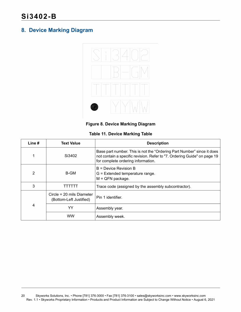
8. Device Marking Diagram
Figure 8. Device Marking Diagram
Table 11. Device Marking Table
Line # Text Value Description
1 Si3402Base part number. This is not the “Ordering Part Number” since it does not contain a specific revision. Refer to "7. Ordering Guide" on page 19 for complete ordering information.
2 B-GMB = Device Revision BG = Extended temperature range.M = QFN package.
3 TTTTTT Trace code (assigned by the assembly subcontractor).
4
Circle = 20 mils Diameter(Bottom-Left Justified) Pin 1 identifier.
YY Assembly year.
WW Assembly week.
Si3402-B
Skyworks Solutions, Inc. • Phone [781] 376-3000 • Fax [781] 376-3100 • [email protected] • www.skyworksinc.com 21Rev. 1.1 • Skyworks Proprietary Information • Products and Product Information are Subject to Change Without Notice • August 6, 2021
DOCUMENT CHANGE LISTRevision 0.4 to Revision 1.0 Updated Table 2 on page 4 to reflect improvements and clarifications for several parameters. Updated Table 3 on page 5 to reflect detailed Si3402-B behaviors, while retaining system-level compatibility
with Si3402-A. Updated Table 7, “Component Listing—Class 0 with 5 V Output,” on page 8 and Table 8, “Components—Class
1 with Isolated 5.0 V Output,” on page 9 to reflect component values that must be changed at the board level to maintain Si3402–A compatibility when using Si3402-B.
Updated Table 8, “Si3402-B Pin Descriptions (Top View),” on page 16 and related diagrams to indicate 4 pins that are not internally connected on Si3402-B (SSFT, ISOSSFT, VPOSS, VSS1) vs. Si3402-A.
Revision 1.0 to Revision 1.1 Deleted Surge Immunity Ratings table. This data is now contained in the Qualification Summary and “AN956:
Si3402-B POE PD Controller Design Guide”. Updated "2. Typical Application Schematics*" on page 7. Added new section, "3.5. Output Voltage and Thermal Considerations" on page 15. Deleted references to Class 4 operation. Updated Figure 3, “Input Lineside and Hotswap Block Diagram,” on page 9 Added Figure 4, “UVLO Behavior and Threshold Voltages,” on page 11. Updated Figure 5, “Switching Regulator Block Diagram,” on page 14 (formerly Figure 4).

Copyright © 2021 Skyworks Solutions, Inc. All Rights Reserved.Information in this document is provided in connection with Skyworks Solutions, Inc. (“Skyworks”) products or services. These materials, including the information contained herein, are provided by Skyworks as a service to its customers and may be used for informational purposes only by the customer. Skyworks assumes no responsibility for errors or omissions in these materials or the information contained herein. Skyworks may change its documentation, products, services, specifications or product descriptions at any time, without notice. Skyworks makes no commitment to update the materials or information and shall have no responsibility whatsoever for conflicts, incompatibilities, or other difficulties arising from any future changes.
No license, whether express, implied, by estoppel or otherwise, is granted to any intellectual property rights by this document. Skyworks assumes no liability for any materials, products or information provided hereunder, including the sale, distribution, reproduction or use of Skyworks products, information or materials, except as may be provided in Skyworks’ Terms and Conditions of Sale.
THE MATERIALS, PRODUCTS AND INFORMATION ARE PROVIDED “AS IS” WITHOUT WARRANTY OF ANY KIND, WHETHER EXPRESS, IMPLIED, STATUTORY, OR OTHERWISE, INCLUDING FITNESS FOR A PARTICULAR PURPOSE OR USE, MERCHANTABILITY, PERFORMANCE, QUALITY OR NON-INFRINGEMENT OF ANY INTELLECTUAL PROPERTY RIGHT; ALL SUCH WARRANTIES ARE HEREBY EXPRESSLY DISCLAIMED. SKYWORKS DOES NOT WARRANT THE ACCURACY OR COMPLETENESS OF THE INFORMATION, TEXT, GRAPHICS OR OTHER ITEMS CONTAINED WITHIN THESE MATERIALS. SKYWORKS SHALL NOT BE LIABLE FOR ANY DAMAGES, INCLUDING BUT NOT LIMITED TO ANY SPECIAL, INDIRECT, INCIDENTAL, STATUTORY, OR CONSEQUENTIAL DAMAGES, INCLUDING WITHOUT LIMITATION, LOST REVENUES OR LOST PROFITS THAT MAY RESULT FROM THE USE OF THE MATERIALS OR INFORMATION, WHETHER OR NOT THE RECIPIENT OF MATERIALS HAS BEEN ADVISED OF THE POSSIBILITY OF SUCH DAMAGE.
Skyworks products are not intended for use in medical, lifesaving or life-sustaining applications, or other equipment in which the failure of the Skyworks products could lead to personal injury, death, physical or environmental damage. Skyworks customers using or selling Skyworks products for use in such applications do so at their own risk and agree to fully indemnify Skyworks for any damages resulting from such improper use or sale.
Customers are responsible for their products and applications using Skyworks products, which may deviate from published specifications as a result of design defects, errors, or operation of products outside of published parameters or design specifications. Customers should include design and operating safeguards to minimize these and other risks. Skyworks assumes no liability for applications assistance, customer product design, or damage to any equipment resulting from the use of Skyworks products outside of Skyworks’ published specifications or parameters.
Skyworks, the Skyworks symbol, Sky5®, SkyOne®, SkyBlue™, Skyworks Green™, Clockbuilder®, DSPLL®, ISOmodem®, ProSLIC®, and SiPHY® are trademarks or registered trademarks of Skyworks Solutions, Inc. or its subsidiaries in the United States and other countries. Third-party brands and names are for identification purposes only and are the property of their respective owners. Additional information, including relevant terms and conditions, posted at www.skyworksinc.com, are incorporated by reference.
Portfoliowww.skyworksinc.com
Qualitywww.skyworksinc.com/quality
Support & Resourceswww.skyworksinc.com/support
Connecting Everyone
and Everything,
All the Time
Skyworks Solutions, Inc. | Nasdaq: SWKS | [email protected] | www.skyworksinc.comUSA: 781-376-3000 | Asia: 886-2-2735 0399 | Europe: 33 (0)1 43548540 |