Embed Size (px)
Citation preview

Preliminary Rev. 0.5 1/11 Copyright © 2011 by Silicon Laboratories Si1141/42/43This information applies to a product under development. Its characteristics and specifications are subject to change without notice.
Si1141/42/43
PROXIMITY/AMBIENT LIGHT SENSOR IC WITH I2C INTERFACE
Features
Applications
Description
The Si1141/42/43 is a low-power, reflectance-based, infrared proximity and ambientlight sensor with I2C digital interface and programmable-event interrupt output. Thistouchless sensor IC includes an analog-to-digital converter, integrated high-sensitivity visible and infrared photodiodes, digital signal processor, and one, two, orthree integrated infrared LED drivers with fifteen selectable drive levels. The Si1141/42/43 offers excellent performance under a wide dynamic range and a variety of lightsources including direct sunlight. The Si1141/42/43 can also work under dark glasscovers. The photodiode response and associated digital conversion circuitry provideexcellent immunity to artificial light flicker noise and natural light flutter noise. Withtwo or more LEDs, the Si1142/43 is capable of supporting multiple-axis proximitymotion detection. The Si1141/42/43 devices are provided in a 10-lead 2x2 mm QFNpackage and are capable of operation from 1.8 to 3.6 V over the –40 to +85 °Ctemperature range.
QuickSense™ integrated infrared proximity detectorProximity detection adjustable from
under 1 cm to over 1 mThree independent LED drivers15 current settings from 5.6 mA to
360 mA for each LED driver25.6 µs LED driver pulse width500 mm proximity range with single
pulse (<2.5 klx)150 mm proximity range with single
pulse (>2.5 klx)Operates at up to 128 klx (direct
sunlight)Minimum reflectance sensitivity
< 1 µW/cm2
High EMI immunity without shielded packaging
QuickSense™ integrated ambient light sensor10 mlx resolution possible, allowing
operation under dark glass1 to 128 klx dynamic range possible
across two ADC range settings17-bit resolution
Accurate lux measurements possible with IR correction algorithm
25.6 µs measurement cycle keeps total power consumption duty cycle low without compromising performance or noise immunity
Industry's lowest power consumption1.8 to 3.6 V supply voltage9 µA average current (LED pulsed
25.6 µs every 800 ms at 180 mA plus 3 µA Si114x supply)
< 500 nA standby currentInternal and external wake supportBuilt-in voltage supply monitor and
power-on reset controller Serial communications
Up to 3.4 Mbps data rateSlave mode hardware address
decoding Small-outline 10-lead 2x2 mm QFN Temperature Range
–40 to +85 °C
Handsets E-book readers Notebooks/Netbooks Portable consumer electronics Audio products Security panels Tamper detection circuits Dispensers
Valve controls Smoke detectors Touchless switches Touchless sliders Occupancy sensors Consumer electronics Industrial automation Display backlighting control Photo-interrupters
Pin Assignments
LED1
VDD
SCL GND
INT
2
3
4
9
8
7
6
QFN-10LED3
LED2
SDA 1
DNC
10
5
NC

Si1141/42/43
2 Preliminary Rev. 0.5
Functional Block Diagram
Figure 1. Si1141 Basic Application
Figure 2. Si1143 Application with Three LEDs and Separate LED Power Supply
Note: For more application examples, refer to “AN498: irLED Selection Guide for Si114x Proximity Applications”.
Visible
VDD
SDA
SCL
Regulator
I2C
LED Drivers
LED1
LED32
LED21
GND
INTInfrared
Registers
AMUX
ADC
TempFilter
Oscillator
Digital Sequencer & Control Logic
1. Si1142 and Si1143 only.2. Si1143 only.
SDA
SCL
VDD
INT
LED1
GND
CVDD
CVDD
Si1141
15 µF, 20%, >6 V
30 ohm5%, 1/16 W
3.3 V
0.1 uF
Host
SDA
SCL
INT
SDA
SCL
VDD
INT
LED1
GND
LED3
LED2
Si1143
22 uF, 20%, >6V
30 ohm5%, 1/16 W
3.3 V
0.1 uF
Host
4.3 V
NoPop

Si1141/42/43
Preliminary Rev. 0.5 3
TABLE OF CONTENTS
Section Page
1. Electrical Specifications . . . . . . . . . . . . . . . . . . . . . . . . . . . . . . . . . . . . . . . . . . . . . . . . . . .42. Functional Description . . . . . . . . . . . . . . . . . . . . . . . . . . . . . . . . . . . . . . . . . . . . . . . . . . . .8
2.1. Introduction . . . . . . . . . . . . . . . . . . . . . . . . . . . . . . . . . . . . . . . . . . . . . . . . . . . . . . . . .82.2. Proximity Sensing (PS) . . . . . . . . . . . . . . . . . . . . . . . . . . . . . . . . . . . . . . . . . . . . . . . .82.3. Ambient Light . . . . . . . . . . . . . . . . . . . . . . . . . . . . . . . . . . . . . . . . . . . . . . . . . . . . . .102.4. Host Interface . . . . . . . . . . . . . . . . . . . . . . . . . . . . . . . . . . . . . . . . . . . . . . . . . . . . . .11
3. Operational Modes . . . . . . . . . . . . . . . . . . . . . . . . . . . . . . . . . . . . . . . . . . . . . . . . . . . . . . .143.1. Off Mode . . . . . . . . . . . . . . . . . . . . . . . . . . . . . . . . . . . . . . . . . . . . . . . . . . . . . . . . . .143.2. Initialization Mode . . . . . . . . . . . . . . . . . . . . . . . . . . . . . . . . . . . . . . . . . . . . . . . . . . .143.3. Standby Mode . . . . . . . . . . . . . . . . . . . . . . . . . . . . . . . . . . . . . . . . . . . . . . . . . . . . . .143.4. Forced Conversion Mode . . . . . . . . . . . . . . . . . . . . . . . . . . . . . . . . . . . . . . . . . . . . .143.5. Autonomous Operation Mode . . . . . . . . . . . . . . . . . . . . . . . . . . . . . . . . . . . . . . . . . .15
4. Programming Guide . . . . . . . . . . . . . . . . . . . . . . . . . . . . . . . . . . . . . . . . . . . . . . . . . . . . . .164.1. Command and Response Structure . . . . . . . . . . . . . . . . . . . . . . . . . . . . . . . . . . . . .164.2. Command Protocol . . . . . . . . . . . . . . . . . . . . . . . . . . . . . . . . . . . . . . . . . . . . . . . . . .174.3. Resource Summary . . . . . . . . . . . . . . . . . . . . . . . . . . . . . . . . . . . . . . . . . . . . . . . . .194.4. Signal Path Software Model . . . . . . . . . . . . . . . . . . . . . . . . . . . . . . . . . . . . . . . . . . .244.5. I2C Registers . . . . . . . . . . . . . . . . . . . . . . . . . . . . . . . . . . . . . . . . . . . . . . . . . . . . . .254.6. Parameter RAM . . . . . . . . . . . . . . . . . . . . . . . . . . . . . . . . . . . . . . . . . . . . . . . . . . . .45
5. Pin Descriptions . . . . . . . . . . . . . . . . . . . . . . . . . . . . . . . . . . . . . . . . . . . . . . . . . . . . . . . . .606. Ordering Guide . . . . . . . . . . . . . . . . . . . . . . . . . . . . . . . . . . . . . . . . . . . . . . . . . . . . . . . . . .617. Package Outline: 10-Pin QFN . . . . . . . . . . . . . . . . . . . . . . . . . . . . . . . . . . . . . . . . . . . . . .62Document Change List . . . . . . . . . . . . . . . . . . . . . . . . . . . . . . . . . . . . . . . . . . . . . . . . . . . . .64Contact Information . . . . . . . . . . . . . . . . . . . . . . . . . . . . . . . . . . . . . . . . . . . . . . . . . . . . . . . .66

Si1141/42/43
4 Preliminary Rev. 0.5
1. Electrical Specifications
Table 1. Recommended Operating Conditions
Parameter Symbol Conditions Min Typ Max Units
VDD Supply Voltage VDD includes ripple 1.8 3.3 3.6 V
VDD OFF Supply Voltage VDD_OFF OFF mode –0.3 1.0 V
VDD Supply Ripple VoltageVDD = 3.3 V
1 kHz–10 MHz— 50 TBD mVpp
Operating Temperature T –40 25 85 °C
SCL, SDA, Input High Logic Voltage
I2CVIH VDDx0.7 — VDD V
SCL, SDA Input Low LogicVoltage
I2CVIL 0 — VDDx0.3 V
PS Operation under Direct Sunlight
Edc — — 128 klx
IrLED Emission Wavelength l 750 850 950 nm
IrLED Supply Voltage VLED IrLED VF = 1.0 V nominal VDD — 4.3 V
IrLED Supply Ripple Voltage
Applies if IrLEDs use separate supply rail
0–30 kHz30 kHz–100 MHz
——
250100
TBDTBD
mVppmVpp
Start-Up Time VDD above 1.8 V 20 — — ms
LED3 Voltage Start-up VDDx0.77 — — V
Table 2. Absolute Maximum Ratings
Parameter Conditions Min Typ Max Units
VDD Supply Voltage –0.3 — 4 V
Operating Temperature –40 — 85 °C
Storage Temperature –65 — 85 °C
LED1, LED2, LED3 Voltage at VDD = 0 V, TA < 85 °C –0.5 — 3.6 V
INT, SCL, SDA Voltage at VDD = 0 V, TA < 85 °C –0.5 — 3.6 V
Maximum total current through LED1, LED2 and LED3
— — 500 mA
Maximum total current through GND
— — 600 mA
ESD Rating Human Body Model — — 2 kV

Si1141/42/43
Preliminary Rev. 0.5 5
Table 3. Performance Characteristics1
Parameter Symbol Conditions Min Typ Max Units
IDD OFF Mode IoffVDD < VDD_OFF (leakage from SCL,
SDA, and INT not included)— 240 1000 nA
IDD Standby Mode Isb
No ALS / PS Conversions No I2C Activity
after t > TBD µs, VDD = 1.8 V— 150 500 nA
IDD Standby Mode Isb
No ALS / PS Conversions No I2C Activity
after t > TBD µs, VDD =3.3 V— 1.83 — µA
IDD Actively Measuring Iactive Without LED influence, VDD = 3.3 V — 4.3 5.2 mA
Peak IDD while LED1, LED2, or LED3 is Actively Driven
VDD = 3.3 V — 8 — mA
LED1, LED2, LED3, Saturation Voltage2
1.8< VDD<2.4, ILEDx<100 mA1.8<VDD<2.4, ILEDx< 200 mA2.4<VDD<3.6, ILEDx<200 mA2.4<VDD<3.6, ILEDx<359 mA
————
0.30.50.30.5
————
V
LED1, LED2, LED3 Pulse Width
tPS — 25.6 30 µs
LED1, LED2, LED3 Leakage Current
VDD = 3.3 V, VLEDx<3.0, no strobeVDD = 3.3 V, 3.0<VLEDx< 5.0, no strobe
——
.011.0
5.05.0
µA
Notes:1. Unless specifically stated in "Conditions", electrical data assumes ambient light levels < 1 klx.2. Proximity-detection performance may be degraded, especially when there is high optical crosstalk, if the LED supply
and voltage drop allow the driver to saturate and current regulation is lost.3. Represents the time during which the device is drawing a current equal to Iactive for power estimation purposes.
Assumes default settings.4. Applies to single 25.6 µs pulse measurement. By increasing irLED pulse width, 0.001 µW/cm2 under low light is
possible.5. ALS Sensitivity under low light conditions can be improved by increasing ADC integration time. 10 mlx resolution
possible under the highest ADC integration time setting.

Si1141/42/43
6 Preliminary Rev. 0.5
LED1, LED2, LED3 Active Current
ILEDx
VDD = 3.3 V, single driveVLEDn = 1 V, PS_LEDn = 0001VLEDn = 1 V, PS_LEDn = 0010VLEDn = 1 V, PS_LEDn = 0011VLEDn = 1 V, PS_LEDn = 0100VLEDn = 1 V, PS_LEDn = 0101VLEDn = 1 V, PS_LEDn = 0110VLEDn = 1 V, PS_LEDn = 0111VLEDn = 1 V, PS_LEDn = 1000VLEDn = 1 V, PS_LEDn = 1001VLEDn = 1 V, PS_LEDn = 1010VLEDn = 1 V, PS_LEDn = 1011VLEDn = 1 V, PS_LEDn = 1100VLEDn = 1 V, PS_LEDn = 1101VLEDn = 1 V, PS_LEDn = 1110VLEDn = 1 V, PS_LEDn = 1111
———————————————
5.611.222.4456790112135157180202224269314359
TBDTBDTBDTBDTBDTBDTBDTBDTBDTBDTBDTBDTBDTBDTBD
mA
Actively Measuring Time3Single PS
ALS VIS + ALS IRTwo ALS plus three PS
———
155285660
TBDTBDTBD
µsµsµs
PS Min Detectable Reflectance Input4
EMINVDD = 3.3 V = 850 nm
— 0.1 1µW/cm2
PS Max Detectable Reflectance Input
EMAXVDD = 3.3 V = 850 nm
25 — —mW/cm2
ALS Range5 10m — 128k lx
ALS Flicker Noise Error VDD = 3.3 V — ±5 — %
SCL, SDA, INT Output Low Voltage
VOLI = 4 mA, VDD > 2.0 V I = 4 mA, VDD < 2.0 V
——
——
VDDx0.20.4
VV
Table 3. Performance Characteristics1 (Continued)
Parameter Symbol Conditions Min Typ Max Units
Notes:1. Unless specifically stated in "Conditions", electrical data assumes ambient light levels < 1 klx.2. Proximity-detection performance may be degraded, especially when there is high optical crosstalk, if the LED supply
and voltage drop allow the driver to saturate and current regulation is lost.3. Represents the time during which the device is drawing a current equal to Iactive for power estimation purposes.
Assumes default settings.4. Applies to single 25.6 µs pulse measurement. By increasing irLED pulse width, 0.001 µW/cm2 under low light is
possible.5. ALS Sensitivity under low light conditions can be improved by increasing ADC integration time. 10 mlx resolution
possible under the highest ADC integration time setting.

Si1141/42/43
Preliminary Rev. 0.5 7
Table 4. I2C Timing Specifications
Parameter Symbol Min Typ Max Unit
Clock Frequency fSCL — — 3.4 MHz
Clock Pulse Width Low tLOW 160 — — ns
Clock Pulse Width High tHIGH 60 — — ns
Rise Time tR 10 — 40 ns
Fall Time tF 10 — 40 ns
Start Condition Hold Time tHD.STA 160 — — ns
Start Condition Setup Time tSU.STA 160 — — ns
Input Data Setup Time tSU.DAT 10 — — ns
Input Data Hold Time tHD.DAT 0 — — ns
Stop Condition Setup Time tSU.STO 160 — — ns

Si1141/42/43
8 Preliminary Rev. 0.5
2. Functional Description
2.1. IntroductionThe Si1141/42/43 is an active optical reflectance proximity detector and ambient light sensor whose operationalstate is controlled through registers accessible through the I2C interface. The host can command the Si1141/42/43to initiate on-demand proximity detection or ambient light sensing. The host can also place the Si1141/42/43 in anautonomous operational state where it performs measurements at set intervals and interrupts the host either aftereach measurement is completed or whenever a set threshold has been crossed. This results in an overall systempower saving allowing the host controller to operate longer in its sleep state instead of polling the Si1141/42/43. Formore details, refer to “AN498: Designer's Guide for the Si114x”.
2.2. Proximity Sensing (PS)The Si1141/42/43 has been optimized for use as either a dual-port or single-port active reflection proximitydetector. Over distances of less than 50 cm, the dual-port active reflection proximity detector has significantadvantages over single-port, motion-based infrared systems, which are only good for triggered events. Motion-based infrared detectors identify objects within proximity, but only if they are moving. Single-port motion-basedinfrared systems are ambiguous about stationary objects even if they are within the proximity field. The Si1141/42/43 can reliably detect an object entering or exiting a specified proximity field, even if the object is not moving or ismoving very slowly. However, beyond about 30–50 cm, even with good optical isolation, single-port signalprocessing may be required due to static reflections from nearby objects, such as table tops, walls, etc. If motiondetection is acceptable, the Si1141/42/43 can achieve ranges of up to 50 cm, through a single product window.
For small objects, the drop in reflectance is as much as the fourth power of the distance. This means that there isless range ambiguity than with passive motion-based devices. For example, a sixteenfold change in an object'sreflectance means only a fifty-percent drop in detection range.
The Si1141/42/43 can drive three separate infrared LEDs. When the three infrared LEDs are placed in an L-shapedconfiguration, it is possible to triangulate an object within the three-dimensional proximity field. Thus, a touchlessuser interface can be implemented with the aid of host software.
The Si1141/42/43 can initiate proximity sense measurements when explicitly commanded by the host orperiodically through an autonomous process. Refer to "3. Operational Modes" on page 14 for additional details ofthe Si1141/42/43's Operational Modes.
Whenever it is time to make a PS measurement, the Si1141/42/43 makes up to three measurements, dependingon what is enabled in the CHLIST parameter. Other ADC parameters for these measurements can also bemodified to allow proper operation under different ambient light conditions.
The LED choice is programmable for each of these three measurements. By default, each measurement turns on asingle LED driver. However, the order of measurements can be easily reversed or even have all LEDs turned on atthe same time. Optionally, each proximity measurement can be compared against a host-programmable threshold.With threshold settings for each PS channel, it is also possible for the Si1141/42/43 to notify the host whenever thethreshold has been crossed. This reduces the number of interrupts to the host, aiding in efficient softwarealgorithms.
The Si1141/42/43 can also generate an interrupt after a complete set of proximity measurements, ignoring anythreshold settings.
To support different power usage cases dynamically, the infrared LED current of each output is independentlyprogrammable. The current can be programmed anywhere from a few to several hundred milliamps. Therefore, thehost can optimize for proximity detection performance or for power saving dynamically. This feature can be usefulsince it allows the host to reduce the LED current once an object has entered a proximity sphere, and the objectcan still be tracked at a lower current setting. Finally, the flexible current settings make it possible to control theinfrared LED currents with a controlled current sink, resulting in higher precision.
The ADC properties are programmable. For indoor operation, the ADC should be configured for low signal rangefor best reflectance sensitivity. When under high ambient conditions, the ADC should be configured for high signallevel range operation.

Si1141/42/43
Preliminary Rev. 0.5 9
When operating in the lower signal range, it is possible to saturate the ADC when the ambient light level is high.Any overflow condition is reported in the RESPONSE register, and the corresponding data registers report a valueof 0xFFFF. The host can then adjust the ADC sensitivity. Note however that the overflow condition is not sticky. Ifthe light levels return to a range within the capabilities of the ADC, the corresponding data registers begin tooperate normally. However, the RESPONSE register will continue to hold the overflow condition until a NOPcommand is received. Even if the RESPONSE register has an overflow condition, commands are still acceptedand processed.
Proximity detection ranges beyond 50 cm and up to several meters can be achieved without lensing by selecting alonger integration time. The detection range may be increased further, even with high ambient light, by averagingmultiple measurements. Refer to “AN498: Designer's Guide for the Si114x” for more details.
Figure 3. Typical Proximity Sense Performance Curves
5
7
9
11
13
15
17
19
21
23
25
0 500 1000 1500 2000 2500 3000 3500 4000 4500
Dis
tanc
e (c
m)
PSLEDx_DATA
47%, Hand, 1 Lux
47%, Hand, 300 Lux Fluorescent
47%, Hand, 300 Lux Incandescent
18% Gray Card, 1 Lux
92% White Card, 1 Lux
5
10
15
20
25
30
35
40
45
50
0 5000 10000 15000 20000 25000 30000
Dis
tanc
e (c
m)
PSLEDx_DATA
47%, Hand, 1 Lux
47%, Hand, 300 Lux Fluorescent
47%, Hand, 300 Lux Incandescent
18% Gray Card, 1 Lux
92% White Card, 1 Lux

Si1141/42/43
10 Preliminary Rev. 0.5
2.3. Ambient LightThe Si1141/42/43 has photodiodes capable of measuring both visible and infrared light. However, the visiblephotodiode is also influenced by infrared light. The measurement of illuminance requires the same spectralresponse as the human eye. If an accurate lux measurement is desired, the extra IR response of the visible-lightphotodiode must be compensated. Therefore, to allow the host to make corrections to the infrared light’s influence,the Si1141/42/43 reports the infrared light measurement on a separate channel. The separate visible and IRphotodiodes lend themselves to a variety of algorithmic solutions. The host can then take these two measurementsand run an algorithm to derive an equivalent lux level as perceived by a human eye. Having the IR correctionalgorithm running in the host allows for the most flexibility in adjusting for system-dependent variables. Forexample, if the glass used in the system blocks visible light more than infrared light, the IR correction needs to beadjusted.
If the host is not making any infrared corrections, the infrared measurement can be turned off in the CHLISTparameter.
By default, the measurement parameters are optimized for indoor ambient light levels where it is possible to detectlight levels as low as 6 lx. For operation under direct sunlight, the ADC can be programmed to operate in a highsignal operation so that it is possible to measure direct sunlight without overflowing the 16-bit result.
For low-light applications, it is possible to increase the ADC integration time. Normally, the integration time is25.6 µs. By increasing this integration time to 410 µs, the ADC can detect light levels as low as 1 lx. The ADC canbe programmed with an integration time as high as 52.4 ms, allowing measurement to 10 mlx light levels. The ADCintegration time for the Visible Light Ambient measurement can be programmed independently of the ADCintegration time of the Infrared Light Ambient measurement. The independent ADC parameters allow operationunder glass covers having a higher transmittance to Infrared Light than Visible Light.
When operating in the lower signal range, or when the integration time is increased, it is possible to saturate theADC when the ambient light suddenly increases. Any overflow condition is reported in the RESPONSE register,and the corresponding data registers report a value of 0xFFFF. Based on either of these two overflow indicators,the host can adjust the ADC sensitivity. However, the overflow condition is not sticky. If the light levels return to arange within the capabilities of the ADC, the corresponding data registers begin to operate normally. TheRESPONSE register will continue to hold the overflow condition until a NOP command is received. Even if theRESPONSE register has an overflow condition, commands are still accepted and processed.
The Si1141/42/43 can initiate ALS measurements either when explicitly commanded by the host or periodicallythrough an autonomous process. Refer to "3. Operational Modes" on page 14 for additional details of the Si1141/42/43's Operational Modes. The conversion frequency setting is programmable and independent of the ProximitySensor. This allows the Proximity Sensor and Ambient Light sensor to operate at different conversion rates,increasing host control over the Si1141/42/43.
When operating autonomously, the ALS has a slightly different interrupt structure compared to the ProximitySensor. An interrupt can be generated to the host on every sample, or when the ambient light has changed.
The “Ambient Light Changed” interrupt is accomplished through two thresholds working together to implement awindow. As long as the ambient light stays within the window defined by the two thresholds, the host is notinterrupted. When the ambient light changes and either threshold is crossed, an interrupt is sent to the host,thereby allowing the host notification that the ambient light has changed. This can be used by the host to trigger arecalculation of the lux values.
The window can be applied to either the Visible Ambient Measurement, or the Infrared Ambient Measurement, butnot both. However, monitoring the ambient change in either channel should allow notification that the ambient lightlevel has changed.

Si1141/42/43
Preliminary Rev. 0.5 11
Figure 4. Typical Ambient Light Sense Performance Curves (Preliminary)
2.4. Host InterfaceThe host interface to the Si1141/42/43 consists of three pins:
SCL
SDA
INT
SCL and SDA are standard open-drain pins as required for I2C operation.
The Si1141/42/43 asserts the INT pin to interrupt the host processor. The INT pin is an open-drain output. A pull-upresistor is needed for proper operation. As an open-drain output, it can be shared with other open-drain interruptsources in the system.
For proper operation, the Si1141/42/43 is expected to fully complete its Initialization Mode prior to any activity onthe I2C.
The INT, SCL, and SDA pins are designed so that it is possible for the Si1141/42/43 to enter the Off Mode bysoftware command without interfering with normal operation of other I2C devices on the bus.
The Si1141/42/43 I2C slave address is 0x5A. The Si1141/42/43 also responds to the global address (0x00) and theglobal reset command (0x06). Only 7-bit I2C addressing is supported; 10-bit I2C addressing is not supported.
Conceptually, the I2C interface allows access to the Si1141/42/43 internal registers. Table 15 on page 25 is asummary of these registers.
An I2C write access always begins with a start (or restart) condition. The first byte after the start condition is the I2Caddress and a read-write bit. The second byte specifies the starting address of the Si1141/42/43 internal register.Subsequent bytes are written to the Si1141/42/43 internal register sequentially until a stop condition isencountered. An I2C write access with only two bytes is typically used to set up the Si1141/42/43 internal addressin preparation for an I2C read.
The I2C read access, like the I2C write access, begins with a start or restart condition. In an I2C read, the I2C

Si1141/42/43
12 Preliminary Rev. 0.5
master then continues to clock SCK to allow the Si1141/42/43 to drive the I2C with the internal register contents.
The Si1141/42/43 also supports burst reads and burst writes. The burst read is useful in collecting contiguous,sequential registers. The Si1141/42/43 register map was designed to optimize for burst reads for interrupthandlers, and the burst writes are designed to facilitate rapid programming of commonly used fields, such asthresholds registers.
The internal register address is a six-bit (bit 5 to bit 0) plus an Autoincrement Disable (on bit 6). The AutoincrementDisable is turned off by default. Disabling the autoincrementing feature allows the host to poll any single internalregister repeatedly without having to keep updating the Si1141/42/43 internal address every time the register isread.
It is recommended that the host should read PS or ALS measurements (in the I2C Register Map) when the Si1141/42/43 asserts INT. Although the host can read any of the Si1141/42/43's I2C registers at any time, care must betaken when reading 2-byte measurements outside the context of an interrupt handler. The host could be readingpart of the 2-byte measurement when the internal sequencer is updating that same measurement coincidentally.When this happens, the host could be reading a hybrid 2-byte quantity whose high byte and low byte are parts ofdifferent samples. If the host must read these 2-byte registers outside the context of an interrupt handler, the hostshould “double-check” a measurement if the measurement deviates significantly from a previous reading.
Figure 5. I2C Bit Timing Diagram
Figure 6. Host Interface Single Write
Figure 7. Host Interface Single Read
Figure 8. Host Interface Burst Write
Figure 9. Host Interface Burst Read
Figure 10. Si1141/42/43 REG ADDRESS Format
SLA6SDA
SLA5-0 R/W D7 D6-0
SCL
Slave Address + R/W Data ByteSTART ACK NACK STOP

Si1141/42/43
Preliminary Rev. 0.5 13
Notes: Gray boxes are driven by the host to the Si1141/42/43
White boxes are driven by the Si1141/42/43 to the host
A = ACK or “acknowledge”
N = NACK or “no acknowledge”
S = START condition
Sr = repeat START condition
P = STOP condition
AI = Disable Auto Increment when set

Si1141/42/43
14 Preliminary Rev. 0.5
3. Operational Modes
The Si1141/42/43 can be in one of many operational modes at any one time. It is important to consider theoperational mode since the mode has an impact on the overall power consumption of the Si1141/42/43. Thevarious modes are:
Off Mode
Initialization Mode
Standby Mode
Forced Conversion Mode
Autonomous Mode
3.1. Off ModeThe Si1141/42/43 is in the Off Mode when VDD is either not connected to a power supply or if the VDD voltage isbelow the stated VDD_OFF voltage described in the electrical specifications. As long as the parameters stated inTable 2, “Absolute Maximum Ratings,” on page 4 are not violated, no current will flow through the Si1141/42/43. Inthe Off Mode, the Si1141/42/43 SCL and SDA pins do not interfere with other I2C devices on the bus. The LED pinswill not draw current through the infrared diodes. Keeping VDD less than VDD_OFF is not intended as a method ofachieving lowest system current draw. The reason is that the ESD protection devices on the SCL, SDA and INTpins also from a current path through VDD. If VDD is grounded for example, then, current flow from system power tosystem ground through the SCL, SDA and INT pull-up resistors and the ESD protection devices.
Allowing VDD to be less than VDD_OFF is intended to serve as a hardware method of resetting the Si1141/42/43without a dedicated reset pin.
The Si1141/42/43 can also reenter the Off Mode upon receipt of either a general I2C reset or if a software resetsequence is initiated. When one of these software methods is used to enter the Off Mode, the Si1141/42/43typically proceeds directly from the Off Mode to the Initialization Mode.
3.2. Initialization ModeWhen power is applied to VDD and is greater than the minimum VDD Supply Voltage stated in Table 1,“Recommended Operating Conditions,” on page 4, the Si1141/42/43 enters its Initialization Mode. In theInitialization Mode, the Si1141/42/43 performs its initial startup sequence. Since the I2C may not yet be active, it isrecommended that no I2C activity occur during this brief Initialization Mode period. The “Start-up time” specificationin Table 1 is the minimum recommended time the host needs to wait before sending any I2C accesses following apower-up sequence. After Initialization Mode has completed, the Si1141/42/43 enters Standby Mode. The hostmust write 0x17 to the HW_KEY register for proper operation.
3.3. Standby ModeThe Si1141/42/43 spends most of its time in Standby Mode. After the Si1141/42/43 completes the InitializationMode sequence, it enters Standby mode. While in Standby Mode, the Si1141/42/43 does not perform any AmbientLight measurements or Proximity Detection functions. However, the I2C interface is active and ready to acceptreads and writes to the Si1141/42/43 registers. The internal Digital Sequence Controller is in its sleep state anddoes not draw much power. In addition, the INT output retains its state until it is cleared by the host.
I2C accesses do not necessarily cause the Si1141/42/43 to exit the Standby Mode. For example, reading Si1141/42/43 registers is accomplished without needing the Digital Sequence Controller to wake from its sleep state.
3.4. Forced Conversion ModeThe Si1141/42/43 can operate in Forced Conversion Mode under the specific command of the host processor. TheForced Conversion Mode is entered if either the ALS_FORCE or the PS_FORCE command is sent. Uponcompletion of the conversion, the Si1141/42/43 can generate an interrupt to the host if the corresponding interruptis enabled. It is possible to initiate both an ALS and multiple PS measurements with one command register writeaccess by using the PSALS_FORCE command.

Si1141/42/43
Preliminary Rev. 0.5 15
3.5. Autonomous Operation ModeThe Si1141/42/43 can be placed in the Autonomous Operation Mode where measurements are performedautomatically without requiring an explicit host command for every measurement. The PS_AUTO, ALS_AUTO andPSALS_AUTO commands are used to place the Si1141/42/43 in the Autonomous Operation Mode.
The Si1141/42/43 updates the I2C registers for PS and ALS automatically. Each measurement is allocated a 16-bitregister in the I2C map. It is possible to operate the Si1141/42/43 without interrupts. When doing so, the host pollrate must be at least twice the frequency of the conversion rates for the host to always receive a newmeasurement. The host can also choose to be notified when these new measurements are available by enablinginterrupts.
The conversion frequencies for the PS and ALS measurements are set up by the host prior to the PS_AUTO,ALS_AUTO, or PSALS_AUTO commands. The host can set a PS conversion frequency different from the ALSconversion frequency. However, they both need to be a multiple of the base conversion frequency in theMEAS_RATE register in the I2C map.
The Si1141/42/43 can interrupt the host when the PS or ALS measurements reach a pre-set threshold. To assist inthe handling of interrupts the registers are arranged so that the interrupt handler can perform an I2C burst readoperation to read the necessary registers, beginning with the interrupt status register, and cycle through the ALSdata registers followed by the individual Proximity readings.

Si1141/42/43
16 Preliminary Rev. 0.5
4. Programming Guide
4.1. Command and Response StructureAll Si1141/42/43 I2C registers (except writes to the COMMAND register) are read or written without waking up theinternal sequencer. A complete list of the I2C registers can be found in "4.5. I2C Registers" on page 25. In additionto the I2C Registers, RAM parameters are memory locations maintained by the internal sequencer. These RAMParameters are accessible through a Command Protocol (see "4.6. Parameter RAM" on page 45). A complete listof the RAM Parameters can be found in "4.6. Parameter RAM" on page 45.
The Si1141/42/43 can operate either in Forced Measurement or Autonomous Mode. When in ForcedMeasurement mode, the Si1141/42/43 does not make any measurements unless the host specifically requests theSi1141/42/43 to do so via specific commands (refer to the Section 3.2). The CHLIST parameter needs to be writtenso that the Si1141/42/43 would know which measurements to make. The parameter MEAS_RATE, when zero,places the internal sequencer in Forced Measurement mode. When in Forced Measurement mode, the internalsequencer wakes up only when the host writes to the COMMAND register. The power consumption is lowest inForced Measurement mode (MEAS_RATE = 0).
The Si1141/42/43 operates in Autonomous Operation mode when MEAS_RATE is non-zero. The MEAS_RATErepresents the time interval at which the Si1141/42/43 wakes up periodically. Once the internal sequencer hasawoken, the sequencer manages an internal PS Counter and ALS Counter based on the PS_RATE andALS_RATE registers.
When the internal PS counter has expired, up to three proximity measurements are made (PS1, PS2 and PS3)depending on which measurements are enabled via the upper bits of the CHLIST Parameter. All three PSmeasurements are performed, in sequence, beginning with the PS1 measurement channel. In the same way, whenthe ALS counter has expired, up to three measurements are made (ALS_VIS, ALS_IR and AUX) depending onwhich measurements are enabled via the upper bits of the CHLIST Parameter. All three measurements are madein the following sequence: ALS_VIS, ALS_IR and AUX.
PS_RATE and ALS_RATE are normally non-zero. A value of zero in PS_RATE or ALS_RATE causes the internalsequencer to never perform that measurement group. Typically, PS_RATE or ALS_RATE represents a value ofone. A value of one essentially states that the specific measurement group is made every time the device wakesup.
It is possible for both the PS Counter and ALS Counter to both expire at the same time. When that occurs, the PSmeasurements are performed before the ALS measurements. When all measurements have been made, theinternal sequencer goes back to sleep until next time, as dictated by the MEAS_RATE parameter.
The operation of the Si1141/42/43 can be described as two measurement groups bound by some common factors.The PS Measurement group consists of the three PS measurements while the ALS Measurement group consists ofthe Visible Light Ambient Measurement (ALS_VIS), the Infrared Light Ambient Measurement (ALS_IR) and theAuxiliary measurement (AUX). Each measurement group has three measurements each. The Channel List(CHLIST) parameter enables the specific measurements for that measurement grouping.
Each measurement (PS1, PS2, PS3, ALS_VIS, ALS_IR, AUX) are controlled through a combination of I2CRegister or Parameter RAM. Tables 5 to 7 below can be used summarize the properties and resources used foreach measurement.

Si1141/42/43
Preliminary Rev. 0.5 17
4.2. Command ProtocolThe I2C map implements a bidirectional message box between the host and the Si1141/42/43 Sequencer. Host-writable I2C registers facilitate host-to-Si1141/42/43 communication, while read-only I2C registers are used forSi1141/42/43-to-host communication.
Unlike the other host-writable I2C registers, the COMMAND register causes the internal sequencer to wake upfrom Standby mode to process the host request.
When a command is executed, the RESPONSE register is updated. Typically, when there is no error, the upperfour bits are zeroes. To allow command tracking, the lower four bits implement a 4-bit circular counter. In general, ifthe upper nibble of the RESPONSE register is non-zero, this indicates an error or the need for special processing.
The PARAM_WR and PARAM_RD registers are additional mailbox registers.
In addition to the registers in the I2C map, there are environmental parameters accessible through the Command/Response interface. These parameters are stored in the internal ram space. These parameters generally takemore I2C accesses to read and write. The Parameter RAM is described in "4.6. Parameter RAM" on page 45.
Table 5. Command Register Summary
COMMAND Register PARAM_WR Register
PARAM_RDRegister
Error Code in RESPONSE Register
DescriptionName Encoding
PARAM_QUERY 100 aaaaa — nnnn nnnn
Reads the parameter pointed to by bit-field [4:0] and writes value to PARAM_RD. See Table 10 for parameters.
PARAM_SET 101 aaaaa dddd dddd nnnn nnnn
Sets parameter pointed by bitfield [4:0] with value in PARAM_WR, and writes value out to PARAM_RD. See Table 10 for parameters.
PARAM_AND 110 aaaaa dddd dddd nnnn nnnn
Performs a bit-wise AND between PARAM_WR and Parameter pointed by bitfield [4:0], writes updated value to PARAM_RD.See Table 10 for parameters.
PARAM_OR 111 aaaaa dddd dddd nnnn nnnn
Performs a bit-wise OR of PARAM_WR and parameter pointed by bitfield [4:0], writes updated value to PARAM_RD. See Table 10 for parameters.
NOP 000 00000 — — Forces a zero into the RESPONSE register
RESET 000 00001 — — Performs a software reset of thefirmware
BUSADDR 000 00010 — — — Modifies I2C address
Reserved 000 00011 — — — —
Reserved 000 00100 — — — —
PS_FORCE 000 00101 — — Forces a single PS measurement
ALS_FORCE 000 00110 — — Forces a single ALS measurement
PSALS_FORCE 000 00111 — — Forces a single PS and ALS measurement

Si1141/42/43
18 Preliminary Rev. 0.5
Reserved 000 01000 — — — —
PS_PAUSE 000 01001 — — Pauses autonomous PS
ALS_PAUSE 000 01010 — — Pauses autonomous ALS
PSALS_PAUSE 000 01011 — — Pauses PS and ALS
Reserved 000 01100 — — —
PS_AUTO 000 01101 — — Starts/Restarts an autonomous PS Loop
ALS_AUTO 000 01110 — — Starts/Restarts an autonomous ALS Loop
PSALS_AUTO 000 01111 — — Starts/Restarts autonomous ALSand PS loop
Reserved 000 1xxxx — — — —
Table 6. Response Register Error Codes
RESPONSE Register Description
0000 ccccNO_ERROR. The lower bit is a circular counter and is incremented every time a command has completed. This allows the host to keep track of commands sent to the Si1141/42/43. The circular counter may be cleared using the NOP command.
1000 0000 INVALID_SETTING. An invalid setting was encountered. Clear using the NOP command.
1000 1000 PS1_ADC_OVERFLOW. Indicates proximity channel one conversion overflow.
1000 1001 PS2_ADC_OVERFLOW. Indicates proximity channel two conversion overflow.
1000 1010 PS3_ADC_OVERFLOW. Indicates proximity channel three conversion overflow.
1000 1100 ALS_VIS_ADC_OVERFLOW. Indicates visible ambient light channel conversion overflow.
1000 1101 ALS_IR_ADC_OVERFLOW. Indicates infrared ambient light channel conversion overflow.
1000 1110 AUX_ADC_OVERFLOW. Indicates auxiliary channel conversion overflow.
Table 5. Command Register Summary (Continued)
COMMAND Register PARAM_WR Register
PARAM_RDRegister
Error Code in RESPONSE Register
DescriptionName Encoding

Si1141/42/43
Preliminary Rev. 0.5 19
4.3.
Res
ou
rce
Su
mm
ary
Tab
le 7
. Res
ou
rce
Su
mm
ary
for
Inte
rru
pts
an
d T
hre
sho
ld C
hec
kin
g
Mea
sure
men
t C
han
nel
Ch
ann
el
En
able
Inte
rru
pt
Sta
tus
Ou
tpu
tIn
terr
up
t E
nab
leIn
terr
up
t M
od
eT
hre
sho
ld
Reg
iste
rsT
hre
sho
ld
Hys
tere
sis
His
tory
C
hec
kin
gA
uto
no
mo
us
Mea
sure
men
t T
ime
Ba
se
Pro
xim
ity
Sen
se 1
EN
_PS
1 in
C
HLI
ST
[0]
PS
1_IN
T in
IR
Q_S
TAT
US
[2]
PS
1_IE
in
IRQ
_EN
AB
LE[2
]P
S1_
IM[1
:0]
in
IRQ
_MO
DE
1[5:
4]P
S1_
TH
[7:0
]
PS
_HY
ST
[7:0
]P
S_H
IST
OR
Y[7
:0]
ME
AS
_R
AT
E[7
:0]
PS
_RA
TE
[7:0
]P
roxi
mity
S
ense
2
EN
_PS
2 in
C
HLI
ST
[1]
PS
2_IN
T in
IR
Q_S
TAT
US
[3]
PS
2_IE
in
IRQ
_EN
AB
LE[3
]P
S2_
IM[1
:0]
in
IRQ
_MO
DE
1[7:
6]P
S2_
TH
[7:0
]
Pro
xim
ity
Sen
se 3
EN
_PS
3 in
C
HLI
ST
[2]
PS
3_IN
T in
IR
Q_S
TAT
US
[4]
PS
3_E
N in
IR
Q_E
NA
BLE
[4]
PS
3_IM
[1:0
] in
IR
Q_M
OD
E2[
1:0]
PS
3_T
H[7
:0]
ALS
Vis
ible
EN
_ALS
_V
IS in
C
HLI
ST
[4]
ALS
_IN
T[1
:0] i
n IR
Q_S
TAT
US
[1:0
]A
LS_I
E[1
:0]
in
IRQ
_EN
AB
LE[1
:0]
ALS
_IM
[2:0
] in
IR
Q_M
OD
E1[
2:0]
ALS
_LO
W_T
H[7
:0] /
A
LS_H
I_T
H[7
:0]
ALS
_HY
ST
[7:0
]A
LS
_H
IST
OR
Y[7
:0]
AL
S_
RA
TE
[7:0
]A
LS IR
E
N_A
LS_I
R in
C
HLI
ST
[5]
Au
xilia
ryM
easu
rem
ent
EN
_AU
X
in
CH
LIS
T[6
]—
——
——
—

Si1141/42/43
20 Preliminary Rev. 0.5
Tab
le 8
. Res
ou
rce
Su
mm
ary
for
LE
D C
ho
ice
and
AD
C P
aram
eter
s
Mea
sure
men
tC
han
nel
LE
D
Sel
ect
ion
AD
C M
od
eA
DC
Ou
tpu
tA
DC
Inp
ut
So
urc
eA
DC
Rec
ov
ery
Co
un
tA
DC
Hig
h S
ign
al M
od
eA
DC
Clo
ck
Div
ider
AD
C A
lign
men
tA
DC
Off
set
Pro
xim
ity
Sen
se 1
PS
1_L
ED
[2:0
] in
P
SL
ED
12
_SE
LE
CT
[2:0
]
PS
_AD
C_
MO
DE
[1:0
] in
P
S_A
DC
_M
ISC
[2:1
]
PS
1_D
ATA
1[7
:0]
/ P
S1_
DA
TA0[
7:0
]P
S1
_A
DC
MU
X[7
:0]
PS
_A
DC
_RE
C in
P
S_A
DC
_CO
UN
TE
R [
6:4]
PS
_RA
NG
E in
P
S_A
DC
_M
ISC
[5]
PS
_AD
C_G
AIN
[3:0
]
PS
1_A
LIG
N in
P
S_
EN
CO
DIN
G[4
]
AD
C_
OF
FS
ET
[7:0
]
Pro
xim
ity
Sen
se 2
PS
2_L
ED
[2:0
] in
P
SL
ED
12
_SE
LE
CT
[6:4
]
PS
2_D
ATA
1[7
:0]
/ P
S2_
DA
TA0[
7:0
]P
S2
_A
DC
MU
X[7
:0]
PS
2_A
LIG
N in
P
S_
EN
CO
DIN
G[5
]
Pro
xim
ity
Sen
se 3
PS
3_L
ED
[2:0
] in
P
SLE
D3
_SE
LEC
T[
2:0
]
PS
3_D
ATA
1[7
:0]
/ P
S3_
DA
TA0[
7:0
]P
S3
_A
DC
MU
X[7
:0]
PS
3_A
LIG
N in
P
S_
EN
CO
DIN
G[6
]
AL
S V
isib
le
——
AL
S_
VIS
_D
ATA
1 /
AL
S_
VIS
_D
ATA
0
VIS
_AD
C_
RE
C in
A
LS
_VIS
_A
DC
_C
OU
NT
ER
[6:4
]
VIS
_RA
NG
E in
A
LS_
VIS
_AD
C_
MIS
C[5
]A
LS
_V
IS_
AD
C_G
AIN
[3
:0]
ALS
_VIS
_ALI
GN
in
ALS
_E
NC
OD
ING
[4]
ALS
IR
A
LS_I
R_
DA
TA1[
7:0
] /
AL
S_I
R_D
ATA
0[7
:0]
IR_
AD
C_R
EC
in
AL
S_
IR_A
DC
_C
OU
NT
ER
[6
:4]
IR_R
AN
GE
in
AL
S_I
R_
AD
C_M
ISC
[5]
ALS
_IR
_AD
C_
GA
IN
[3:0
]A
LS
_IR
_A
LIG
N in
A
LS_
EN
CO
DIN
G[5
]
Au
xilia
ry
Me
asu
rem
ent
AU
X_D
ATA
1[7
:0] /
A
UX
_DA
TA0
[7:0
]A
UX
_A
DC
MU
X[7
:0]
——
——
Si1141/42/43
Preliminary Rev. 0.5 21
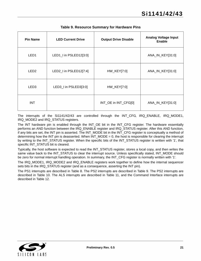
The interrupts of the Si1141/42/43 are controlled through the INT_CFG, IRQ_ENABLE, IRQ_MODE1,IRQ_MODE2 and IRQ_STATUS registers.
The INT hardware pin is enabled through the INT_OE bit in the INT_CFG register. The hardware essentiallyperforms an AND function between the IRQ_ENABLE register and IRQ_STATUS register. After this AND function,if any bits are set, the INT pin is asserted. The INT_MODE bit in the INT_CFG register is conceptually a method ofdetermining how the INT pin is deasserted. When INT_MODE = 0, the host is responsible for clearing the interruptby writing to the INT_STATUS register. When the specific bits of the INT_STATUS register is written with '1', thatspecific INT_STATUS bit is cleared.
Typically, the host software is expected to read the INT_STATUS register, stores a local copy, and then writes thesame value back to the INT_STATUS to clear the interrupt source. Unless specifically stated, INT_MODE shouldbe zero for normal interrupt handling operation. In summary, the INT_CFG register is normally written with '1'.
The IRQ_MODE1, IRQ_MODE2 and IRQ_ENABLE registers work together to define how the internal sequencersets bits in the IRQ_STATUS register (and as a consequence, asserting the INT pin).
The PS1 interrupts are described in Table 8. The PS2 interrupts are described in Table 9. The PS2 interrupts aredescribed in Table 10. The ALS interrupts are described in Table 11, and the Command Interface interrupts aredescribed in Table 12.
Table 9. Resource Summary for Hardware Pins
Pin Name LED Current Drive Output Drive DisableAnalog Voltage Input
Enable
LED1 LED1_I in PSLED12[3:0] ANA_IN_KEY[31:0]
LED2 LED2_I in PSLED12[7:4] HW_KEY[7:0] ANA_IN_KEY[31:0]
LED3 LED3_I in PSLED3[3:0] HW_KEY[7:0]
INT INT_OE in INT_CFG[0] ANA_IN_KEY[31:0]

Si1141/42/43
22 Preliminary Rev. 0.5
Table 10. PS1 Channel Interrupt Resources
IRQ_ENABLE[2] IRQ_MODE1[5:4]Description
PS1_IE PS1_IM[1:0]
0 0 0 No PS1 Interrupts
1 0 0 IRQ_STATUS[2] set after every PS1 sample
1 0 1 IRQ_STATUS[2] set whenever PS1 threshold (PS1_TH) is crossed
1 1 1IRQ_STATUS[2] set whenever PS1 sample is above PS1 threshold (PS1_TH)
Note: There is hysteresis applied (PS_HYST) and history checking (PS_HISTORY). PS1_TH, PS_HYST and are encoded in 8-bit compressed format.
Table 11. PS2 Channel Interrupt Resources
IRQ_ENABLE[3] IRQ_MODE1[7:6]Description
PS2_IE PS2_IM[1:0]
0 0 0 No PS2 Interrupts
1 0 0 IRQ_STATUS[3] set after every PS2 sample
1 0 1 IRQ_STATUS[3] set whenever PS2 threshold (PS2_TH) is crossed
1 1 1 IRQ_STATUS[3] set when PS2 sample is above PS2 threshold (PS2_TH)
Note: There is hysteresis applied (PS_HYST) and history checking (PS_HISTORY). PS2_TH and PS_HYST are encoded in 8-bit compressed format.
Table 12. PS3 Channel Interrupt Resources
IRQ_ENABLE[4] IRQ_MODE2[1:0]Description
PS3_IE PS3_IM[1:0]
0 0 0 No PS3 Interrupts
1 0 0 IRQ_STATUS[4] set after every PS3 sample
1 0 1 IRQ_STATUS[4] set whenever PS3 threshold (PS3_TH) is crossed
1 1 1IRQ_STATUS[4] set whenever PS3 sample is above PS3 threshold (PS3_TH)
Note: There is hysteresis applied (PS_HYST) and history checking (PS_HISTORY). PS3_TH and PS_HYST are encoded in 8-bit compressed format.

Si1141/42/43
Preliminary Rev. 0.5 23
Table 13. Ambient Light Sensing Interrupt Resources
IRQ_ENABLE[1:0] IRQ_MODE1[2:0]Description
ALS_IE[1:0] ALS_IM[2:0]
0 0 0 0 0 No ALS Interrupts
0 1 0 0 0 IRQ_STATUS[0] set after every ALS_VIS sample1
x 1 x 0 1Monitors ALS_VIS, IRQ_STATUS[0] upon exiting region between low and high thresholds (ALS_LOW_TH and ALS_HI_TH)
1 x 1 0 xMonitors ALS_VIS, IRQ_STATUS[1] set upon entering region between low and high thresholds (ALS_LOW_TH and ALS_HI_TH)
x 1 x 1 1Monitors ALS_IR, IRQ_STATUS[0] set upon exiting region between low and high thresholds (ALS_LOW_TH and ALS_HI_TH)
1 x 1 1 xMonitors ALS_IR, IRQ_STATUS[1] set upon entering region between low and high thresholds (ALS_LOW_TH and ALS_HI_TH)
Notes:1. For ALS_IR channel, interrupts per sample is not possible without also enabling ALS_VIS2. All other combinations are invalid and may result in unintended operation3. There is hysteresis applied (ALS_TH) and history checking (ALS_HISTORY). ALS_LOW_TH, ALS_HI_TH,
ALS_HYST are encoded in 8-bit compressed format.
Table 14. Command Interrupt Resources
IRQ_ENABLE[5] IRQ_MODE1[3:2]Description
CMD_IE CMD_IM[1:0]
0 x 0 No CMD Interrupts
1 x 0 IRQ_STATUS[5] set when there is a new RESPONSE
1 x 1 IRQ_STATUS[5] set when there is a new error code in RESPONSE

Si1141/42/43
24 Preliminary Rev. 0.5
4.4. Signal Path Software ModelThe following diagram gives an overview of the signal paths, along with the I2C register and RAM Parameter bitfields that control them. Sections with detailed descriptions of the I2C registers and Parameter RAM follow.
Figure 11. Signal Path Programming Model
PS1_ALIGN
16
ALS_IR_ALIGN
PS1_ADCMUX
16
16
16
16
16
AUX_ADCMUX
PS_RANGEPS_ADC_GAINPS_ADC_RECPS_RATE
PS_RANGEPS_ADC_GAINPS_ADC_RECPS_RATE
PS_RANGEPS_ADC_GAINPS_ADC_RECPS_RATE
VIS_RANGEALS_VIS_ADC_GAINALS_VIS_ADC_RECALS_RATE
IR_RANGEALS_IR_ADC_GAINALS_IR_ADC_RECALS_RATE
ALS_VIS_ALIGN
PS2_ALIGN
PS3_ALIGN
PS2_ADCMUX
PS3_ADCMUX
Ref.
Ref.
Ref.
ADC_OFFSET
ADC_OFFSET
ADC_OFFSET
ADC_OFFSET
ADC_OFFSET
16
ADC_OFFSET
EN_AUX
EN_ALS_IR
EN_ALS_VIS
EN_PS3
EN_PS2
EN_PS1
ALS_IR_ADCMUX
PS1_DATA
PS2_DATA
PS3_DATA
ALS_VIS_DATA
ALS_IR_DATA
AUX_DATA
Vdd
Vdd
Vdd
Vdd
GND
GND
GND
GND
GND
GND
Select
Out0x65
0x75
In
Sum
Offset
Enable
In
Sum
Offset
Enable
Ra
ng
e
Analog Digital
Ga
inR
eco
v. t
ime
Ra
teA
lign
Small visibleSmall visible
Ra
ng
e
Analog Digital
Ga
inR
eco
v. t
ime
Ra
teA
lign
Small IRSmall IR
Select
02360x25
Out
0x650x75
Select
02360x25
Out
0x650x75
Select
Out0
3
Select
02360x25
Out
0x650x75
In
Sum
Offset
Enable
In
Sum
Offset
Enable
Large IRLarge IR
In
Sum
Offset
Enable
In
Sum
Offset
Enable
Analog DigitalTemperaturesensorTemperaturesensor
Ra
ng
e
Analog Digital
Ga
inR
eco
v. t
ime
Ra
teA
lign
Ra
ng
e
Analog Digital
Ga
inR
eco
v. t
ime
Ra
teA
lign
Ra
ng
e
Analog Digital
Ga
inR
eco
v. t
ime
Ra
teA
lign

Si1141/42/43
Preliminary Rev. 0.5 25
4.5. I2C Registers
Table 15. I2C Register Summary
I2C Register Name Address 7 6 5 4 3 2 1 0
PART_ID 0x00 PART_ID
REV_ID 0x01 REV_ID
SEQ_ID 0x02 SEQ_ID
INT_CFG 0x03 INT_MODE INT_OE
IRQ_ENABLE 0x04 CMD_IE PS3_IE PS2_IE PS1_IE ALS_IE
IRQ_MODE1 0x05 PS2_IM PS1_IM ALS_IM
IRQ_MODE2 0x06 CMD_IM PS3_IM
HW_KEY 0x07 HW_KEY
MEAS_RATE 0x08 MEAS_RATE
ALS_RATE 0x09 ALS_RATE
PS_RATE 0x0A PS_RATE
ALS_LOW_TH 0x0B ALS_LOW_TH
Reserved 0x0C Reserved
ALS_HI_TH 0x0D ALS_HI_TH
ALS_IR_ADCMUX 0x0E ALS_IR_ADCMUX
PS_LED21 0x0F LED2_I LED1_I
PS_LED3 0x10 LED3_I
PS1_TH 0x11 PS1_TH
Reserved 0x12 Reserved
PS2_TH 0x13 PS2_TH
Reserved 0x14 Reserved
PS3_TH 0x15 PS3_TH
Reserved 0x16 Reserved
PARAM_WR 0x17 PARAM_WR
COMMAND 0x18 COMMAND
RESPONSE 0x20 RESPONSE
IRQ_STATUS 0x21 CMD_INT PS3_INT PS2_INT PS1_INT ALS_INT
ALS_VIS_DATA0 0x22 ALS_VIS_DATA0
ALS_VIS_DATA1 0x23 ALS_VIS_DATA1
ALS_IR_DATA0 0x24 ALS_IR_DATA0

Si1141/42/43
26 Preliminary Rev. 0.5
ALS_IR_DATA1 0x25 ALS_IR_DATA1
PS1_DATA0 0x26 PS1_DATA0
PS1_DATA1 0x27 PS1_DATA1
PS2_DATA0 0x28 PS2_DATA0
PS2_DATA1 0x29 PS2_DATA1
PS3_DATA0 0x2A PS3_DATA0
PS3_DATA1 0x2B PS3_DATA1
AUX_DATA0 0x2C AUX_DATA0
AUX_DATA1 0x2D AUX_DATA1
PARAM_RD 0x2E PARAM_RD
CHIP_STAT 0x30 RUNNING SUSPEND SLEEP
ANA_IN_KEY0x3B–0x3E
ANA_IN_KEY
Table 15. I2C Register Summary (Continued)
I2C Register Name Address 7 6 5 4 3 2 1 0

Si1141/42/43
Preliminary Rev. 0.5 27
Reset value = 0100 0001 (Si1141)Reset value = 0100 0010 (Si1142)Reset value = 0100 0011 (Si1143)
Reset value = 0000 0001
Reset value = 0000 1000
PART_ID @ 0x00
Bit 7 6 5 4 3 2 1 0
Name PART_ID
Type R
REV_ID @ 0x1
Bit 7 6 5 4 3 2 1 0
Name REV_ID
Type R
SEQ_ID @ 0x02
Bit 7 6 5 4 3 2 1 0
Name SEQ_ID
Type R
Bit Name Function
7:0 SEQ_ID
Sequencer Revision.
0x01 Si114x-A01 (MAJOR_SEQ=0, MINOR_SEQ=1)0x02 Si114x-A02 (MAJOR_SEQ=0, MINOR_SEQ=2)0x03 Si114x-A03 (MAJOR_SEQ=0, MINOR_SEQ=3)0x08 Si114x-A10 (MAJOR_SEQ=1, MINOR_SEQ=0)

Si1141/42/43
28 Preliminary Rev. 0.5
Reset value = 0000 0000
INT_CFG @ 0x03
Bit 7 6 5 4 3 2 1 0
Name INT_MODE INT_OE
Type RW RW
Bit Name Function
7:2 Reserved Reserved.
1 INT_MODE
Interrupt Mode.
The INT_MODE describes how the bits in the IRQ_STATUS Registers are cleared.0: The IRQ_STATUS Register bits are set by the internal sequencer and are sticky. It is the host's responsibility to clear the interrupt status bits in the IRQ_STATUS register to clear the interrupt.1: If the Parameter Field PSx_IM = 11, the internal sequencer clears the INT pin auto-matically.
0 INT_OE
INT Output Enable.
INT_OE controls the INT pin drive0: INT pin is never driven1: INT pin driven low whenever an IRQ_STATUS and its corresponding IRQ_ENABLE bits match

Si1141/42/43
Preliminary Rev. 0.5 29
Reset value = 0000 0000
IRQ_ENABLE @ 0x04
Bit 7 6 5 4 3 2 1 0
Name CMD_IE PS3_IE PS2_IE PS1_IE ALS_IE
Type RW RW RW RW RW
Bit Name Function
7:6 Reserved Reserved.
5 CMD_IE
Command Interrupt Enable.
Enables interrupts based on COMMAND/RESPONSE activity.0: INT never asserts due to COMMAND/RESPONSE interface activity.1: Assert INT pin whenever CMD_INT is set by the internal sequencer.
4 PS3_IE
PS3 Interrupt Enable.
Enables interrupts based on PS3 Channel Activity.0: INT never asserts due to PS3 Channel activity.1: Assert INT pin whenever PS3_INT is set by the internal sequencer.
3 PS2_IE
PS2 Interrupt Enable.
Enables interrupts based on PS2 Channel Activity.0: INT never asserts due to PS2 Channel activity.1: Assert INT pin whenever PS2_INT is set by the internal sequencer.
2 PS1_IE
PS1 Interrupt Enable.
Enables interrupts based on PS1 Channel Activity.0: INT never asserts due to PS1 Channel activity.1: Assert INT pin whenever PS1_INT is set by the internal sequencer.
1:0 ALS_IE
ALS Interrupt Enable.
Enables interrupts based on ALS Activity.00: INT never asserts due to ALS activity.x1: Assert INT pin whenever ALS_INT[1] bit is set by the internal sequencer.1x: Assert INT pin whenever ALS_INT[0] is set by the internal sequencer.

Si1141/42/43
30 Preliminary Rev. 0.5
Reset value = 0000 0000
IRQ_MODE1 @ 0x05
Bit 7 6 5 4 3 2 1 0
Name PS2_IM PS1_IM ALS_IM
Type RW RW RW
Bit Name Function
7:6 PS2_IM
PS2 Interrupt Mode applies only when PS2_IE is also set.00: PS2_INT is set whenever a PS2 measurement has completed.01: PS2_INT is set whenever the current PS2 measurement crosses the PS2_TH threshold.11: PS2_INT is set whenever the current PS2 measurement is greater than the PS2_TH threshold.
5:4 PS1_IM
PS1 Interrupt Mode applies only when PS1_IE is also set.00: PS1_INT is set whenever a PS1 measurement has completed.01: PS1_INT is set whenever the current PS1 measurement crosses the PS1_TH threshold.11: PS1_INT is set whenever the current PS1 measurement is greater than the PS1_TH threshold.
3 Reserved Reserved.
2:0 ALS_IM
ALS Interrupt Mode function is defined in conjunction with ALS_IE[1:0].ALS_IE[1:0] / ALS_IM[2:0]:00 / 000: Neither IRQ_STATUS[1] nor IRQ_STATUS[0] are ever set.01 / 000: IRQ_STATUS[0] sets after every ALS_VIS sample.x1 / x01: Monitors ALS_VIS channel, IRQ_STATUS[0] asserts if measurement exits window between ALS_LOW_TH and ALS_HIGH_TH.x1 / x11: Monitors ALS_IR channel, IRQ_STATUS[0] asserts if measurement exits win-dow between ALS_LOW_TH and ALS_HIGH_TH.1x / x01: Monitors ALS_VIS channel, IRQ_STATUS[1] asserts if measurement enters window between ALS_LOW_TH and ALS_HIGH_TH.1x / x11: Monitors ALS_IR channel, IRQ_STATUS[1] asserts if measurement enters window between ALS_LOW_TH and ALS_HIGH_TH.
Note: The ALS_IM description apples only to sequencer revisions A03 or later.

Si1141/42/43
Preliminary Rev. 0.5 31
Reset value = 0000 0000
Reset value = 0000 0000
IRQ_MODE2 @ 0x06
Bit 7 6 5 4 3 2 1 0
Name CMD_IM PS3_IM
Type RW RW
Bit Name Function
7:4 Reserved Reserved.
3:2 CMD_IM
Command Interrupt Mode applies only when CMD_IE is also set.00: CMD_INT is set whenever the RESPONSE register is written.01: CMD_INT is set whenever the RESPONSE register is written with an error code (MSB set).1x: Reserved.
1:0 PS3_IM
PS3 Interrupt Mode applies only when PS3_IE is also set.00: PS3_INT is set whenever a PS3 measurement has completed.01: PS3_INT is set whenever the current PS3 measurement crosses the PS3_TH threshold.11: PS1_INT is set whenever the current PS1 measurement is greater than the PS3_TH threshold.
HW_KEY @ 0x07
Bit 7 6 5 4 3 2 1 0
Name HW_KEY
Type RW
Bit Name Function
7:0 HW_KEY The system must write the value 0x17 to this register for proper Si114x operation.

Si1141/42/43
32 Preliminary Rev. 0.5
Reset value = 0000 0000
Reset value = 0000 0000
MEAS_RATE @ 0x08
Bit 7 6 5 4 3 2 1 0
Name MEAS_RATE
Type RW
Bit Name Function
7:0 MEAS_RATE
MEAS_RATE is an 8-bit compressed value representing a 16-bit integer. The uncompressed 16-bit value, when multiplied by 31.25 us, represents the time dura-tion between wake-up periods where measurements are made.Example Values:0x00: The device does not make any autonomous measurements0x84: The device wakes up every 10 ms (0x140 x 31.25 µs)0x94: The device wakes up every 20 ms (0x280 x 31.25 µs)0xB9: The device wakes up every 100 ms (0x0C80 x 31.25 µs)0xDF: The device wakes up every 496 ms (0x3E00 x 31.25 µs)0xFF: The device wakes up every 1.984 seconds (0xF800 x 31.25 µs)
ALS_RATE @ 0x09
Bit 7 6 5 4 3 2 1 0
Name ALS_RATE
Type RW
Bit Name Function
7:0 ALS_RATE
ALS_RATE is an 8-bit compressed value representing a 16-bit multiplier. This multi-plier, in conjunction with the MEAS_RATE time, represents how often ALS Measure-ments are made.Example Values:0x00: Autonomous ALS Measurements are not made.0x08: ALS Measurements made every time the device wakes up. (0x0001 x timeValueOf(MEAS_RATE))0x32: ALS Measurements made every 10 times the device wakes up. (0x000A x timeValueOf(MEAS_RATE)0x69: ALS Measurements made every 100 times the device wakes up. (0x0064 x timeValueOf(MEAS_RATE)

Si1141/42/43
Preliminary Rev. 0.5 33
Reset value = 0000 0000
Reset value = 0000 0000
PS_RATE @ 0x0A
Bit 7 6 5 4 3 2 1 0
Name PS_RATE
Type RW
Bit Name Function
7:0 PS_RATE
PS_RATE is an 8-bit compressed value representing a 16-bit multiplier. This multiplier, in conjunction with the MEAS_RATE time, represents how often PS Measurements are made.Example Values:0x00: Autonomous PS Measurements are not made0x08: PS Measurements made every time the device wakes up (0x0001 x timeValueOf(MEAS_RATE))0x32: PS Measurements made every 10 times the device wakes up (0x000A x timeValueOf(MEAS_RATE)0x69: PS Measurements made every 100 times the device wakes up (0x0064 x timeValueOf(MEAS_RATE)
ALS_LOW_TH @ 0x0B
Bit 7 6 5 4 3 2 1 0
Name ALS_LOW_TH
Type RW
Bit Name Function
7:0 ALS_LOW_TH
ALS_LOW_TH is an 8-bit compressed value representing a 16-bit threshold value. The uncompressed value represented by ALS_LOW_TH (when used in conjunction with uncompressed value represented by ALS_HI_TH) forms a window region applied to ALS_VIS or ALS_IR measurements for interrupting the host.

Si1141/42/43
34 Preliminary Rev. 0.5
Reset value = 0000 0000
Reset value = 0000 0000
ALS_HI_TH @ 0x0D
Bit 7 6 5 4 3 2 1 0
Name ALS_HI_TH
Type RW
Bit Name Function
7:0 ALS_HI_TH
ALS_HI_TH is an 8-bit compressed value representing a 16-bit threshold value. The uncompressed value represented by ALS_HI_TH (when used in conjunction with uncompressed value represented by ALS_LOW_TH) forms a window region applied to ALS_VIS or ALS_IR measurements for interrupting the host.
Note: This register available for sequencer revisions A03 or later.
ALS_IR_ADCMUX @ 0x0E
Bit 7 6 5 4 3 2 1 0
Name ALS_IR_ADCMUX
Type RW
Bit Name Function
7:0 ALS_IR_ADCMUX
Selects ADC Input for ALS_IR Measurement.
0x00: Small IR photodiode0x03: Large IR photodiode

Si1141/42/43
Preliminary Rev. 0.5 35
Reset value = 0000 0000
PS_LED21 @ 0x0F
Bit 7 6 5 4 3 2 1 0
Name LED2_I LED1_I
Type RW RW
Bit Name Function
7:4 LED2_I LED2_I Represents the irLED current sunk by the LED2 pin during a PS measurement.On the Si1141, these bits must be set to zero.
3:0 LED1_1
LED1_I Represents the irLED current sunk by the LED1 pin during a PS measurement.
LED3_I, LED2_I, and LED1_I current encoded as follows:0000: No current0001: Minimum current1111: Maximum currentRefer to Table 3, “Performance Characteristics1,” on page 5 for LED current values.

Si1141/42/43
36 Preliminary Rev. 0.5
Reset value = 0000 0000
Reset value = 0000 0000
Reset value = 0000 0000
PS_LED3 @ 0x10
Bit 7 6 5 4 3 2 1 0
Name LED3_I
Type RW
Bit Name Function
7:4 Reserved Reserved.
3:0 LED3_ILED3_I Represents the irLED current sunk by the LED3 pin during a PS measure-ment. See PS_LED21 Register for additional details.On the Si1141 and Si1142, these bits must be set to zero.
PS1_TH @ 0x11
Bit 7 6 5 4 3 2 1 0
Name PS1_TH
Type RW
Bit Name Function
7:0 PS1_THPS1_TH is an 8-bit compressed value representing a 16-bit threshold value. The uncom-pressed value represented by PS1_TH is compared to PS1 measurements during auton-omous operation for interrupting the host.
PS2_TH @ 0x13
Bit 7 6 5 4 3 2 1 0
Name PS2_TH
Type RW
Bit Name Function
7:0 PS2_THPS2_TH is an 8-bit compressed value representing a 16-bit threshold value. The uncompressed value represented by PS2_TH is compared to PS2 measurements dur-ing autonomous operation for interrupting the host.

Si1141/42/43
Preliminary Rev. 0.5 37
Reset value = 0000 0000
Reset value = 0000 0000
Reset value = 0000 0000
PS3_TH @ 0x15
Bit 7 6 5 4 3 2 1 0
Name PS3_TH
Type RW
Bit Name Function
7:0 PS3_THPS3_TH is an 8-bit compressed value representing a 16-bit threshold value. The uncompressed value represented by PS3_TH is compared to PS3 measurements during autonomous operation for interrupting the host.
PARAM_WR @ 0x17
Bit 7 6 5 4 3 2 1 0
Name PARAM_WR
Type RW
Bit Name Function
7:0 PARAM_WR Mailbox register for passing parameters from the host to the sequencer.
COMMAND @ 0x18
Bit 7 6 5 4 3 2 1 0
Name COMMAND
Type RW
Bit Name Function
7:0 COMMAND
COMMAND Register.
The COMMAND Register is the primary mailbox register into the internal sequencer.Writing to the COMMAND register is the only I2C operation that wakes the device from standby mode.

Si1141/42/43
38 Preliminary Rev. 0.5
Reset value = 0000 0000
RESPONSE @ 0x20
Bit 7 6 5 4 3 2 1 0
Name RESPONSE
Type RW
Bit Name Function
7:0 RESPONSE
The Response register is used in conjunction with command processing. When an error is encountered, the response register will be loaded with an error code. All error codes will have the MSB is set.The error code is retained until a RESET or NOP command is received by the sequencer. Other commands other than RESET or NOP will be ignored. However, any autonomous operation in progress continues normal operation despite any error.0x00–0x0F: No Error. Note that bits 3:0 form an incrementing roll-over counter.0x80: Invalid Command Encountered during command processing0x88: ADC Overflow encountered during PS1 measurement0x89: ADC Overflow encountered during PS2 measurement0x8A: ADC Overflow encountered during PS3 measurement0x8C: ADC Overflow encountered during ALS-VIS measurement0x8D: ADC Overflow encountered during ALS-IR measurement0x8E: ADC Overflow encountered during AUX measurement

Si1141/42/43
Preliminary Rev. 0.5 39
Reset value = 0000 0000
Reset value = 0000 0000
IRQ_STATUS @ 0x21
Bit 7 6 5 4 3 2 1 0
Name CMD_INT PS3_INT PS2_INT PS1_INT ALS_INT
Type RW RW RW RW RW
Bit Name Function
7:6 Reserved Reserved.
5 CMD_INT Command Interrupt Status.
4 PS3_INT PS3 Interrupt Status.
3 PS2_INT PS3 Interrupt Status.
2 PS1_INT PS1 Interrupt Status.
1:0 ALS_INT ALS Interrupt Status.
Notes:1. If the corresponding IRQ_ENABLE bit is also set when the IRQ_STATUS bit is set, the INT pin is asserted.2. When INT_MODE = 0, the host must write '1' to the corresponding XXX_INT bit to clear the interrupt.3. When INT_MODE = 1, the internal sequencer clears all the XXX_INT bits (and INT pin) automatically unless used with
PS (Parameter Field PSx_IM = 11). Use of INT_MODE = 0 is recommended.
ALS_VIS_DATA0 @ 0x22
Bit 7 6 5 4 3 2 1 0
Name ALS_VIS_DATA0
Type RW
Bit Name Function
7:0 ALS_VIS_DATA0 ALS VIS Data LSB.

Si1141/42/43
40 Preliminary Rev. 0.5
Reset value = 0000 0000
Reset value = 0000 0000
Reset value = 0000 0000
ALS_VIS_DATA1 @ 0x23
Bit 7 6 5 4 3 2 1 0
Name ALS_VIS_DATA1
Type RW
Bit Name Function
7:0 ALS_VIS_DATA1 ALS VIS Data MSB.
ALS_IR_DATA0 @ 0x24
Bit 7 6 5 4 3 2 1 0
Name ALS_IR_DATA0
Type RW
Bit Name Function
7:0 ALS_IR_DATA0 ALS IR Data LSB.
ALS_IR_DATA1 @ 0x25
Bit 7 6 5 4 3 2 1 0
Name ALS_IR_DATA1
Type RW
Bit Name Function
7:0 ALS_IR_DATA1 ALS IR Data MSB.

Si1141/42/43
Preliminary Rev. 0.5 41
Reset value = 0000 0000
Reset value = 0000 0000
Reset value = 0000 0000
PS1_DATA0 @ 0x26
Bit 7 6 5 4 3 2 1 0
Name PS1_DATA0
Type RW
Bit Name Function
7:0 PS1_DATA0 PS1 Data LSB.
PS1_DATA1 @ 0x27
Bit 7 6 5 4 3 2 1 0
Name PS1_DATA1
Type RW
Bit Name Function
7:0 PS1_DATA1 PS1 Data MSB.
PS2_DATA0 @ 0x28
Bit 7 6 5 4 3 2 1 0
Name PS2_DATA0
Type RW
Bit Name Function
7:0 PS2_DATA0 PS2 Data LSB.

Si1141/42/43
42 Preliminary Rev. 0.5
Reset value = 0000 0000
Reset value = 0000 0000
Reset value = 0000 0000
PS2_DATA1 @ 0x29
Bit 7 6 5 4 3 2 1 0
Name PS2_DATA1
Type RW
Bit Name Function
7:0 PS2_DATA1 PS2 Data MSB.
PS3_DATA0 @ 0x2A
Bit 7 6 5 4 3 2 1 0
Name PS3_DATA0
Type RW
Bit Name Function
7:0 PS3_DATA0 PS3 Data LSB.
PS3_DATA1 @ 0x2B
Bit 7 6 5 4 3 2 1 0
Name PS3_DATA1
Type RW
Bit Name Function
7:0 PS3_DATA1 PS3 Data MSB.
Si1141/42/43
Preliminary Rev. 0.5 43
Reset value = 0000 0000
Reset value = 0000 0000
Reset value = 0000 0000
AUX_DATA0 @ 0x2C
Bit 7 6 5 4 3 2 1 0
Name AUX_DATA0
Type RW
Bit Name Function
7:0 AUX_DATA0 AUX Data LSB.
AUX_DATA1 @ 0x2D
Bit 7 6 5 4 3 2 1 0
Name AUX_DATA1
Type RW
Bit Name Function
7:0 AUX_DATA1 AUX Data MSB.
PARAM_RD @ 0x2E
Bit 7 6 5 4 3 2 1 0
Name PARAM_RD
Type RW
Bit Name Function
7:0 PARAM_RD Mailbox register for passing parameters from the sequencer to the host.

Si1141/42/43
44 Preliminary Rev. 0.5
Reset value = 0000 0000
Reset value = 0000 0000
CHIP_STAT @ 0x30
Bit 7 6 5 4 3 2 1 0
Name RUNNING SUSPEND SLEEP
Type R R R
Bit Name Function
7:3 Reserved Reserved
2 RUNNING Device is awake.
1 SUSPEND Device is in a low-power state, waiting for a measurement to complete.
0 SLEEP Device is in its lowest power state.
ANA_IN_KEY @ 0x3B to 0x3E
Bit 7 6 5 4 3 2 1 0
0x3B ANA_IN_KEY[31:24]
0x3C ANA_IN_KEY[23:16]
0x3D ANA_IN_KEY[15:8]
0x3E ANA_IN_KEY[7:0]
Type RW
Bit Name Function
31:0 ANA_IN_KEY[31:0] Reserved.

Si1141/42/43
Preliminary Rev. 0.5 45
4.6. Parameter RAM
Table 16. Parameter RAM Summary Table
Parameter Name Offset Bit 7 Bit 6 Bit 5 Bit 4 Bit 3 Bit 2 Bit 1 Bit 0
I2C_ADDR 0x00 I2C Address
CHLIST 0x01 — EN_AUX EN_ALS_IR EN_ALS_VIS — EN_PS3 EN_PS2 EN_PS1
PSLED12_SELECT 0x02 — PS2_LED — PS1_LED
PSLED3_SELECT 0x03 — PS3_LED
Reserved 0x04 Reserved (always set to 0)
PS_ENCODING 0x05 — PS3_ALIGN PS2_ALIGN PS1_ALIGN Reserved (always set to 0)
ALS_ENCODING 0x06 — ALS_IR_ALIGNALS_VIS_
ALIGNReserved (always set to 0)
PS1_ADCMUX 0x07 PS1 ADC Input Selection
PS2_ADCMUX 0x08 PS2 ADC Input Selection
PS3_ADCMUX 0x09 PS3 ADC Input Selection
PS_ADC_COUNTER 0x0A — PS_ADC_REC Reserved (always set to 0)
PS_ADC_GAIN 0x0B — PS_ADC_GAIN
PS_ADC_MISC 0x0C — PS_RANGE — PS_ADC_MODE —
Reserved 0x0D Reserved (do not modify from default setting of 0x00)
Reserved 0x0E Reserved (do not modify from default setting of 0x02)
AUX_ADCMUX 0x0F AUX ADC Input Selection
ALS_VIS_ADC_COUNTER 0x10 — VIS_ADC_REC Reserved (always set to 0)
ALS_VIS_ADC_GAIN 0x11 — ALS_VIS_ADC_GAIN
ALS_VIS_ADC_MISC 0x12Reserved
(always set to 0)VIS_RANGE Reserved (always set to 0)
Reserved 0x13 Reserved (do not modify from default setting of 0x40)
Reserved0x14–0x15
Reserved (do not modify from default setting of 0x00)
ALS_HYST 0x16 ALS Hysteresis
PS_HYST 0x17 PS Hysteresis
PS_HISTORY 0x18 PS History Setting
ALS_HISTORY 0x19 ALS History Setting
ADC_OFFSET 0x1A ADC Offset
Reserved 0x1B Reserved (do not modify from default setting of 0x00)
LED_REC 0x1C LED recovery time
ALS_IR_ADC_COUNTER 0x1D — IR_ADC_REC Reserved (always set to 0)
ALS_IR_ADC_GAIN 0x1E — ALS_IR_ADC_GAIN
ALS_IR_ADC_MISC 0x1FReserved
(always set to 0)IR_RANGE Reserved (always set to 0)

Si1141/42/43
46 Preliminary Rev. 0.5
Reset value = 0000 0000
Reset value = 0000 0000
I2C @ 0x00
Bit 7 6 5 4 3 2 1 0
Name I2C Address
Type RW
Bit Name Function
7:0 I2C AddressSpecifies a new I2C Address for the device to respond to. The new address takes effect when a BUSADDR command is received.
CHLIST @ 0x01
Bit 7 6 5 4 3 2 1 0
Name EN_AUX EN_ALS_IR EN_ALS_VIS EN_PS3 EN_PS2 EN_PS1
Type RW RW
Bit Name Function
7 Reserved Reserved.
6 EN_AUX Enables Auxiliary Channel, data stored in AUX_DATA1[7:0] and AUX_DATA0[7:0].
5 EN_ALS_IR Enables ALS IR Channel, data stored in ALS_IR_DATA1[7:0] and ALS_IR_DATA0[7:0].
4 EN_ALS_VISEnables ALS Visible Channel, data stored in ALS_VIS_DATA1[7:0] and ALS_VIS_DATA0[7:0].
3 Reserved Reserved.
2 EN_PS3 Enables PS Channel 3, data stored in PS3_DATA1[7:0] and PS3_DATA0[7:0].
1 EN_PS2 Enables PS Channel 2, data stored in PS2_DATA1[7:0] and PS2_DATA0[7:0].
0 EN_PS1 Enables PS Channel 1, data stored in PS1_DATA1[7:0] and PS1_DATA0[7:0].

Si1141/42/43
Preliminary Rev. 0.5 47
Reset value = 0010 0001
PSLED12_SELECT @ 0x02
Bit 7 6 5 4 3 2 1 0
Name PS2_LED PS1_LED
Type RW RW
Bit Name Function
7 Reserved Reserved.
6:4 PS2_LED
Specifies the LED pin driven during the PS2 Measurement. Note that any combination of irLEDs is possible.000: NO LED DRIVExx1: LED1 Drive Enabledx1x: LED2 Drive Enabled (Si1142 and Si1143 only. Clear for Si1141)1xx: LED3 Drive Enabled (Si1143 only. Clear for Si1141 and Si1142)
3 Reserved Reserved.
2:0 PS1_LED
Specifies the LED pin driven during the PS1 Measurement. Note that any combination of irLEDs is possible.000: NO LED DRIVExx1: LED1 Drive Enabledx1x: LED2 Drive Enabled (Si1142 and Si1143 only. Clear for Si1141)1xx: LED3 Drive Enabled (Si1143 only. Clear for Si1141 and Si1142)

Si1141/42/43
48 Preliminary Rev. 0.5
Reset value = 0000 0100
Reset value = 0000 0000
PSLED3_SELECT @ 0x03
Bit 7 6 5 4 3 2 1 0
Name PS3_LED
Type RW
Bit Name Function
7:3 Reserved Reserved.
2:0 PS3_LED
Specifies the LED pin driven during the PS3 Measurement. Note that any combination of irLEDs is possible.000: No LED drive.xx1: LED1 drive enabled.x1x: LED2 drive enabled (Si1142 and Si1143 only. Clear for Si1141).1xx: LED3 drive enabled (Si1143 only. Clear for Si1141 and Si1142).
PS_ENCODING @ 0x05
Bit 7 6 5 4 3 2 1 0
Name PS3_ALIGN PS2_ALIGN PS1_ALIGN
Type RW
Bit Name Function
7 Reserved Reserved.
6 PS3_ALIGN When set, the ADC reports the least significant 16 bits of the 17-bit ADC when performing PS3 Measurement. Reports the 16 MSBs when cleared.
5 PS2_ALIGN When set, the ADC reports the least significant 16 bits of the 17-bit ADC when performing PS2 Measurement. Reports the 16 MSBs when cleared.
4 PS1_ALIGN When set, the ADC reports the least significant 16 bits of the 17-bit ADC when performing PS1 Measurement. Reports the 16 MSBs when cleared.
3:0 Reserved Reserved (always set to 0).

Si1141/42/43
Preliminary Rev. 0.5 49
Reset value = 0000 0000
ALS_ENCODING @ 0x06
Bit 7 6 5 4 3 2 1 0
Name ALS_IR_ALIGN ALS_VIS_ALIGN
Type RW RW
Bit Name Function
7:6 Reserved Reserved.
5 ALS_IR_ALIGN When set, the ADC reports the least significant 16 bits of the 17-bit ADC when performing ALS VIS Measurement. Reports the 16 MSBs when cleared.
4 ALS_VIS_ALIGN When set, the ADC reports the least significant 16 bits of the 17-bit ADC when performing ALS IR Measurement. Reports the 16 MSBs when cleared.
3:0 Reserved Reserved (always set to 0).

Si1141/42/43
50 Preliminary Rev. 0.5
Reset value = 0000 0011
PS1_ADCMUX @ 0x07
Bit 7 6 5 4 3 2 1 0
Name PS1_ADCMUX
Type RW
Bit Name Function
7:0 PS1_ADCMUX
Selects ADC Input for PS1 Measurement.
The following selections are valid when PS_ADC_MODE = 1 (default). This setting is for normal Proximity Detection function.0x03: Large IR Photodiode0x00: Small IR PhotodiodeIn addition, the following selections are valid for PS_ADC_MODE = 0. With this set-ting, irLED drives are disabled and the PS channels are no longer operating in normal Proximity Detection function. The results have no reference and the references needs to be measured in a separate measurement.0x02: Visible PhotodiodeA separate 'No Photodiode' measurement should be subtracted from this reading. Note that the result is a negative value. The result should therefore be negated to arrive at the Ambient Visible Light reading.0x03: Large IR PhotodiodeA separate “No Photodiode” measurement should be subtracted to arrive at Ambient IR reading.0x00: Small IR PhotodiodeA separate “No Photodiode” measurement should be subtracted to arrive at Ambient IR reading.0x06: No PhotodiodeThis is typically used as reference for reading ambient IR or visible light.0x25: GND voltageThis is typically used as the reference for electrical measurements.0x65: Temperature (Should be used only for relative temperature measurement. Absolute Temperature not guaranteed) A separate GND measurement should be subtracted from this read-ing.0x75: VDD voltageA separate GND measurement is needed to make the measurement meaningful.

Si1141/42/43
Preliminary Rev. 0.5 51
Reset value = 0000 0011
Reset value = 0000 0011
PS2_ADCMUX @ 0x08
Bit 7 6 5 4 3 2 1 0
Name PS2_ADCMUX
Type RW
Bit Name Function
7:0 PS2_ADCMUX Selects input for PS2 measurement. See PS1_ADCMUX register description for details.
PS3_ADCMUX @ 0x09
Bit 7 6 5 4 3 2 1 0
Name PS3_ADCMUX
Type RW
Bit Name Function
7:0 PS3_ADCMUX Selects input for PS3 measurement. See PS1_ADCMUX register description for details.

Si1141/42/43
52 Preliminary Rev. 0.5
Reset value = 0111 0000
Reset value = 0000 0000
PS_ADC_COUNTER @ 0x0A
Bit 7 6 5 4 3 2 1 0
Name PS_ADC_REC
Type RW
Bit Name Function
7 Reserved Reserved.
6:4 PS_ADC_REC
Recovery period the ADC takes before making a PS measurement.000: 1 ADC Clock (50 ns)001: 7 ADC Clock (350 ns)010: 15 ADC Clock (750 ns)011: 31 ADC Clock (1.55 µs)100: 63 ADC Clock (3.15 µs)101: 127 ADC Clock (6.35 µs)110: 255 ADC Clock (12.75 µs)111: 511 ADC Clock (25.55 µs)
3:0 Reserved Reserved (always set to 0).
PS_ADC_GAIN @ 0x0B
Bit 7 6 5 4 3 2 1 0
Name PS_ADC_GAIN
Type RW
Bit Name Function
7:4 Reserved Reserved.
3:0 PS_ADC_GAIN
Increases the irLED pulse width and ADC integration time by a factor of (2 ^ PS_ADC_GAIN) for all PS measurements.Care must be taken when using this feature. At an extreme case, each of the three PS measurements can be configured to drive three separate irLEDs, each of which, are configured for 359 mA. The internal sequencer does not protect the device from such an error. To prevent permanent damage to the device, do not enter any value greater than 5 without consulting with Silicon Labs.For Example:0x0: ADC Clock is divided by 10x4: ADC Clock is divided by 160x5: ADC Clock is divided by 32
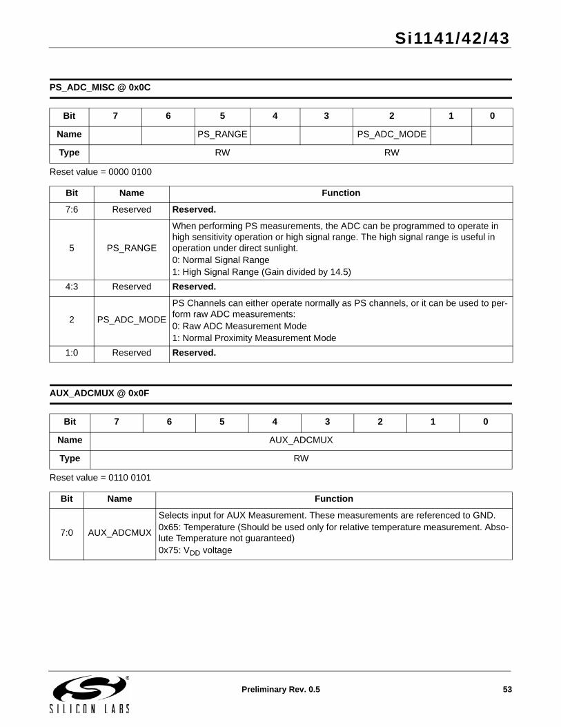
Si1141/42/43
Preliminary Rev. 0.5 53
Reset value = 0000 0100
Reset value = 0110 0101
PS_ADC_MISC @ 0x0C
Bit 7 6 5 4 3 2 1 0
Name PS_RANGE PS_ADC_MODE
Type RW RW
Bit Name Function
7:6 Reserved Reserved.
5 PS_RANGE
When performing PS measurements, the ADC can be programmed to operate in high sensitivity operation or high signal range. The high signal range is useful in operation under direct sunlight.0: Normal Signal Range1: High Signal Range (Gain divided by 14.5)
4:3 Reserved Reserved.
2 PS_ADC_MODE
PS Channels can either operate normally as PS channels, or it can be used to per-form raw ADC measurements:0: Raw ADC Measurement Mode1: Normal Proximity Measurement Mode
1:0 Reserved Reserved.
AUX_ADCMUX @ 0x0F
Bit 7 6 5 4 3 2 1 0
Name AUX_ADCMUX
Type RW
Bit Name Function
7:0 AUX_ADCMUX
Selects input for AUX Measurement. These measurements are referenced to GND.0x65: Temperature (Should be used only for relative temperature measurement. Abso-lute Temperature not guaranteed)0x75: VDD voltage

Si1141/42/43
54 Preliminary Rev. 0.5
Reset value = 0111 0000
Reset value = 0000 0000
ALS_VIS_ADC_COUNTER @ 0x10
Bit 7 6 5 4 3 2 1 0
Name VIS_ADC_REC
Type RW
Bit Name Function
7 Reserved Reserved.
6:4 VIS_ADC_REC
Recovery period the ADC takes before making a ALS-VIS measurement.000: 1 ADC Clock (50 ns)001: 7 ADC Clock (350 ns)010: 15 ADC Clock (750 ns)011: 31 ADC Clock (1.55 µs)100: 63 ADC Clock (3.15 µs)101: 127 ADC Clock (6.35 µs)110: 255 ADC Clock (12.75 µs)111: 511 ADC Clock (25.55 µs)
3:0 Reserved Reserved. Always set to 0.
Note: For A02 and earlier, this parameter also controls ALS-IR measurements.
ALS_VIS_ADC_GAIN @ 0x11
Bit 7 6 5 4 3 2 1 0
Name ALS_VIS_ADC_GAIN
Type RW
Bit Name Function
7:4 Reserved Reserved.
3:0 ALS_VIS_ADC_GAIN
Increases the ADC integration time for ALS Visible measurements by a factor of (2 ^ ALS_VIS_ADC_GAIN). This allows visible light measure-ment under dark glass.For Example:0x0: ADC Clock is divided by 10x4: ADC Clock is divided by 160x6: ADC Clock is divided by 64
Note: For A02 and earlier, this parameter also controls ALS-IR measurements.

Si1141/42/43
Preliminary Rev. 0.5 55
Reset value = 0000 0000
Reset value = 0100 1000
ALS_VIS_ADC_MISC @ 0x12
Bit 7 6 5 4 3 2 1 0
Name VIS_RANGE
Type RW
Bit Name Function
7:6 Reserved Reserved.
5 VIS_RANGE
When performing ALS-VIS measurements, the ADC can be programmed to operate in high sensitivity operation or high signal range.The high signal range is useful in operation under direct sunlight.0: Normal Signal Range1: High Signal Range (Gain divided by 14.5)
4:0 Reserved Reserved.
Note: For A02 and earlier, this parameter also controls ALS-IR measurements.
ALS_HYST @ 0x16
Bit 7 6 5 4 3 2 1 0
Name ALS_HYST
Type RW
Bit Name Function
7:0 ALS_HYSTALS_HYST represents a hysteresis applied to the ALS_LOW_TH and ALS_HIGH_TH thresholds. This is in an 8-bit compressed format, representing a 16-bit value. For example:0x48: 24 ADC Codes

Si1141/42/43
56 Preliminary Rev. 0.5
Reset value = 0100 1000
Reset value = 0000 0011
PS_HYST @ 0x17
Bit 7 6 5 4 3 2 1 0
Name PS_HYST
Type RW
Bit Name Function
7:0 PS_HYSTPS_HYST represents a hysteresis applied to the PS1_TH, PS2_TH and PS3_TH thresh-olds. This is in an 8-bit compressed format, representing a 16-bit value. For example: 0x48: 24 ADC Codes.
PS_HISTORY @ 0x18
Bit 7 6 5 4 3 2 1 0
Name PS_HISTORY
Type RW
Bit Name Function
7:0 PS_HISTORY
PS_HISTORY is a bit-field representing the number of consecutive samples exceeding the threshold and hysteresis to change status.For example:0x03: 2 consecutive samples0x07: 3 consecutive samples0xFF: 8 consecutive samples

Si1141/42/43
Preliminary Rev. 0.5 57
Reset value = 0000 0011
Reset value = 1000 0000
ALS_HISTORY @ 0x19
Bit 7 6 5 4 3 2 1 0
Name ALS_HISTORY
Type RW
Bit Name Function
7:0 ALS_HISTORY
ALS_HISTORY is a bit-field representing the number of consecutive samples exceeding the threshold and hysteresis to change status.For example:0x03: Two consecutive samples0x07: Three consecutive samples0xFF: Eight consecutive samples
ADC_OFFSET @ 0x1A
Bit 7 6 5 4 3 2 1 0
Name ADC_OFFSET
Type RW
Bit Name Function
7:0 ADC_OFFSET
ADC_OFFSET is an 8-bit compressed value representing a 16-bit value added to all measurements. Since most measurements are relative measurements involving a arith-metic subtraction and can result in a negative value. Since 0xFFFF is treated as an overrange indicator, the ADC_OFFSET is added so that the values reported in the I2C register map are never confused with the 0xFFFF overrange indicator.For example:0x60: Measurements have a 64-code offset0x70: Measurements have a 128-code offset0x80: Measurements have a 256-code offset

Si1141/42/43
58 Preliminary Rev. 0.5
Reset value = 0000 0000
Reset value = 0111 0000
LED_REC @ 0x1C
Bit 7 6 5 4 3 2 1 0
Name LED_REC
Type RW
Bit Name Function
7:0 LED_REC Reserved.
ALS_IR_ADC_COUNTER @ 0x1D
Bit 7 6 5 4 3 2 1 0
Name IR_ADC_REC
Type RW
Bit Name Function
7 Reserved Reserved.
6:4 IR_ADC_REC
Recovery period the ADC takes before making a ALS-IR measurement.000: 1 ADC Clock (50 ns)001: 7 ADC Clock (350 ns)010: 15 ADC Clock (750 ns)011: 31 ADC Clock (1.55 µs)100: 63 ADC Clock (3.15 µs)101: 127 ADC Clock (6.35 µs)110: 255 ADC Clock (12.75 µs)111: 511 ADC Clock (25.55 µs)
3:0 Reserved Reserved (always set to 0).
Note: This parameter available for sequencer revisions A03 or later.

Si1141/42/43
Preliminary Rev. 0.5 59
Reset value = 0000 0000
Reset value = 0000 0100
ALS_IR_ADC_GAIN @ 0x1E
Bit 7 6 5 4 3 2 1 0
Name ALS_IR_ADC_GAIN
Type RW
Bit Name Function
7:4 Reserved Reserved.
3:0 ALS_IR_ADC_GAIN
Increases the ADC integration time for IR Ambient measurements by a factor of (2 ^ ALS_IR_ADC_GAIN).For Example:0x0: ADC Clock is divided by 10x4: ADC Clock is divided by 160x6: ADC Clock is divided by 64
Note: This parameter available for sequencer revisions A03 or later.
ALS_IR_ADC_MISC @ 0x1F
Bit 7 6 5 4 3 2 1 0
Name IR_RANGE
Type RW
Bit Name Function
7:6 Reserved Reserved.
5 IR_RANGE
When performing ALS-IR measurements, the ADC can be programmed to operate in high sensitivity operation or high signal range.The high signal range is useful in operation under direct sunlight.0: Normal Signal Range1: High Signal Range (Gain divided by 14.5)
4:0 ReservedReserved: Write operations to this RAM parameter must preserve this bit-field value using read-modify-write.
Note: This parameter is available for sequencer revisions A03 or later.

Si1141/42/43
60 Preliminary Rev. 0.5
5. Pin Descriptions
Table 17. Pin Descriptions
Pin Name Type Description
1 SDA Bidirectional I2C Data.
2 SCL Input I2C Clock.
3 VDD PowerPower Supply.Voltage source.
4 INT BidirectionalInterrupt Output.Open-drain interrupt output pin. Must be at logic level high during power-up sequence to enable low power operation.
5 NCNo Connect.This pin is not electrically connected to any internal Si1141/42/43 node.
6 LED21 OutputLED2 Output.1
Programmable constant current sink normally connected to an infrared LED cathode.
7 LED32 Output
LED3 Output.2
Programmable constant current sink normally connected to an infrared LED cathode. If VLED < (VDD + 0.5 V), a 47 k pull-up resistor from LED3 to VDD is needed for proper operation. Connect directly to VDD when not in use.
8 GND PowerGround.Reference voltage.
9 LED1 OutputLED1 Output.Programmable constant current sink normally connected to an infrared LED cathode.
10 DNCDo Not Connect.This pin is electrically connected to an internal Si1141/42/43 node. It should remain unconnected.
Notes:1. Si1142 and Si1143 only. Connect to VDD in Si1141.2. Si1143 only. Connect to VDD in Si1141 and Si1142.
LED1
VDD
SCL GND
INT
2
3
4
9
8
7
6
QFN-10LED3
LED2
SDA 1
DNC
10
5
NC

Si1141/42/43
Preliminary Rev. 0.5 61
6. Ordering Guide
Part Number Package LED Drivers
Si1141-A10-GM QFN-10 1
Si1142-A10-GM QFN-10 2
Si1143-A10-GM QFN-10 3

Si1141/42/43
62 Preliminary Rev. 0.5
7. Package Outline: 10-Pin QFN
Figure 12 illustrates the package details for the Si1141/42/43 QFN package. Table 18 lists the values for thedimensions shown in the illustration.
Figure 12. QFN Package Diagram Dimensions
Table 18. Package Diagram Dimensions
Dimension Min Nom Max
A 0.55 0.65 0.75
b 0.20 0.25 0.30
D 2.00 BSC.
e 0.50 BSC.
E 2.00 BSC.
L 0.30 0.35 0.40
aaa 0.10
bbb 0.10
ccc 0.08
ddd 0.10
Notes:1. All dimensions shown are in millimeters (mm).2. Dimensioning and Tolerancing per ANSI Y14.5M-1994.
Pin 1 Indication
Top View

Si1141/42/43
Preliminary Rev. 0.5 63
Figure 13. Photodiode Centers
0.35
1.21
0.59
0.18
0.19
0.70
Large IR Photodiode
Small IR PhotodiodeVisible Photodiode(stacked photodiodes)
Pin 1

Si1141/42/43
64 Preliminary Rev. 0.5
DOCUMENT CHANGE LIST
Revision 0.2 to Revision 0.3 Updated document title from Si1140 to Si114x.
Updated "7. Package Outline: 10-Pin QFN" on page 62.
Updated Tables 2, 1, and 3.
Added Figures 1, 3, and 4.
Added register map and descriptions.
Revision 0.3 to Revision 0.4 Updated document title from Si114x to Si1143.
Updated Applications Section
Updated Tables 2 and 3.
Updated Figure 1, Figure 4.
Updated Table 8, Table 9.
Updated Pin Assignments.
Updated Register maps and description.
Revision 0.4 to Revision 0.41 Added Si1141 and Si1142 in addition to Si1143.
Added the ODFN-8 package option.
Some sections were rearranged.
Added the signal-path software-model schematic.
Renamed PARAM_IN to PARAM_WR for clarity.
Renamed PARAM_OUT to PARAM_RD for clarity.
Renamed PS_ADC_CLKDIV to PS_ADC_GAIN for clarity.
Renamed ALS_VIS_ADC_CLKDIV to ALS_VIS_ADC_GAIN for clarity.
Renamed ALS_IR_ADC_CLKDIV to ALS_IR_ADC_GAIN for clarity.
Minor changes in register and parameter terminology.
Revision 0.41 to Revision 0.5 Updated Tables 1, 2, 3, and 15.
Updated Figure 1.
Added Figures 2 and 13.
Updated register table reset values.
Added “ HW_KEY @ 0x07” register.
Updated “ALS_VIS_ADC_MISC @ 0x12” register.
Updated “ALS_IR_ADC_MISC @ 0x1F” register.
Updated “6. Ordering Guide” .
Updated “ Features” .
Updated “ Description” .
Updated “5. Pin Descriptions” .
Updated “6. Ordering Guide” .
Updated “7. Package Outline: 10-Pin QFN” .
Deleted Section 7.1.
Deleted Section 7.2.

Si1141/42/43
Preliminary Rev. 0.5 65
NOTES:

Si1141/42/43
66 Preliminary Rev. 0.5
CONTACT INFORMATIONSilicon Laboratories Inc.
400 West Cesar ChavezAustin, TX 78701Tel: 1+(512) 416-8500Fax: 1+(512) 416-9669Toll Free: 1+(877) 444-3032
Please visit the Silicon Labs Technical Support web page:https://www.silabs.com/support/pages/contacttechnicalsupport.aspxand register to submit a technical support request.
Silicon Laboratories and Silicon Labs are trademarks of Silicon Laboratories Inc.Other products or brandnames mentioned herein are trademarks or registered trademarks of their respective holders.
The information in this document is believed to be accurate in all respects at the time of publication but is subject to change without notice. Silicon Laboratories assumes no responsibility for errors and omissions, and disclaims responsibility for any consequences resulting from the use of information included herein. Additionally, Silicon Laboratories assumes no responsibility for the functioning of undescribed features or parameters. Silicon Laboratories reserves the right to make changes without further notice. Silicon Laboratories makes no warranty, rep-resentation or guarantee regarding the suitability of its products for any particular purpose, nor does Silicon Laboratories assume any liability arising out of the application or use of any product or circuit, and specifically disclaims any and all liability, including without limitation conse-quential or incidental damages. Silicon Laboratories products are not designed, intended, or authorized for use in applications intended to support or sustain life, or for any other application in which the failure of the Silicon Laboratories product could create a situation where per-sonal injury or death may occur. Should Buyer purchase or use Silicon Laboratories products for any such unintended or unauthorized ap-plication, Buyer shall indemnify and hold Silicon Laboratories harmless against all claims and damages.