Embed Size (px)
Citation preview
Chalmers University of Technology Department of Signals and Systems Göteborg, Sweden, June 2011
Short-Slot Hybrid Coupler in Gap Waveguides at 38 GHz Master of Science Thesis in Wireless and Photonics Engineering 2011
BILAL HUSSAIN
2
The Author grants to Chalmers University of Technology the non-exclusive right to publish the
Work electronically and in a non-commercial purpose make it accessible on the Internet.
The Author warrants that he/she is the author to the Work, and warrants that the Work does not
contain text, pictures or other material that violates copyright law.
The Author shall, when transferring the rights of the Work to a third party (for example a
publisher or a company), acknowledge the third party about this agreement. If the Author has
signed a copyright agreement with a third party regarding the Work, the Author warrants hereby
that he/she has obtained any necessary permission from this third party to let Chalmers
University of Technology store the Work electronically and make it accessible on the Internet.
Short-Slot Hybrid Coupler in Gap Waveguides at 38 GHz
BILAL HUSSAIN
© BILAL HUSSAIN, June 2011.
Examiner: PER-SIMON KILDAL
Technical report no 2011:xx
Antenna Group, Department of Signals & Systems
Chalmers University of Technology
SE-41296 Goteborg
Sweden
Telephone +46 (0) 31-772 1000
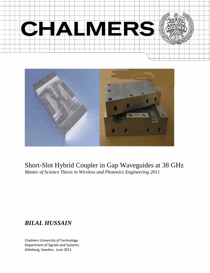
Cover: Picture shows manufactured Short-Slot hybrid coupler, it was taken at antenna department in
Chalmers University of Technology and is a property of the department.
Department of Signals and Systems Göteborg, Sweden June 2011

3
I would like to dedicate my work to my parents. Their support and guidance always
enlightened the path of success for me.

4
Acknowledgements
My heartiest gratitude to all those who supported me during this thesis work. I
am really grateful to
Prof, Per-Simon Kildal for his support and guidance throughout this thesis.
He has provided me with the opportunity to work with him in the first
place. Throughout this thesis work, he was always there whenever I
needed. The knowledge that I possess in the field of microwave and
antennas, has a huge contribution from him. Under his supervision I have
learnt a lot and this experience will cherish my memories for the rest of my
life.
Mr. Ashraf Uz Zaman for being so nice and helpful throughout this project.
He was always available to answer my questions. After discussing with him,
I always found the problems solved in a simple and understandable way. A
large portion of this thesis work is based on his ideas and research. I really
regard and thank his efforts for making this possible.
Mr. Tomas Ostling, without his support it was never possible. He always
shared his R & D experience and guided me on the right path. I really
appreciate his punctuality and humbleness. He was always an easy to talk
person. I am really thankful to him.
Dr, Jian Yang, for his support and theoretical knowledge he was delivered
during the antennas course.
Anders Edquist from ansoft support team, who has always provided me
help with HFSS. I really owe him for his availability during the crucial stages
of this thesis.
Syed Hassan Raza, for being a nice office mate and also for clarifying my
concepts.

5
Syed Kashan Ali, for his moral support during hard times. He was always
there to boast up my moral.
Ali Imran Sandhu, for the knowledge he has provided me for HFSS at the
very start of my thesis
Engr, Ashiq Hussain, who not only supported me as a father but also
inspired me to work harder. He was always there to guide me on the right
course of action.
The research group at antenna department and all the students of MPMPE.
You all have contributed directly or indirectly. I am really thankful to you all
for making my masters a life time experience.
6
Abstract
This thesis is an attempt to validate the recently developed gap waveguide
technology. Gap waveguides are modified form of conventional microstrip and
hollow waveguides. It provides two alternatives such as ridge gap waveguide and
groove gap waveguide. This thesis mainly encapsulates the groove gap
waveguides. Groove gap waveguides have similarities with hollow rectangular
waveguides. This fact is used in this thesis by designing a short-slot hybrid coupler
in groove gap waveguides, which is based on the techniques of rectangular
waveguides. The hybrid coupler is designed in Q band with a 7.7% bandwidth.
In chapter 1, the need for this new technology is motivated by explaining the
problems with traditional. Mechanical imperfections and strong electrical contact
problems pose serious challenges to component design at high frequencies.
Chapter 2 explains the comparison of different types of couplers with focus on
short-slot hybrid coupler in rectangular waveguides. Chapter 3 mainly concerns
the theoretical and analytical approach behind gap waveguides technology. It
shows the required designing techniques and similarities with conventional
technologies. Most of the text and figures are taken from the research papers
published by Prof,Per-Simon Kildal and his colleagues. References are provided to
the best of author’s knowledge.
Chapter 4 uses the knowledge of chapter 2 & 3, and explains a procedure to
design a 3dB coupler in groove gap waveguides at 38 GHz to meet those
specifications that are valid for 3dB couplers in normal rectangular waveguide.
The method for designing is explained in detail, also some other design variations
are discussed at the end of this chapter. Chapter 5 explains the flexibility of
groove gap waveguides by presenting a coupler of chapter 4 designed to interface
with standard rectangular waveguides. It also shed some light on mechanical
issues related to groove gap waveguide. Finally chapter 6 validates the results of
chapter 4 & 5 by presenting the actual measurements performed on the device. It
also establishes the fact that gap waveguide technology can be used for designing
high frequency components with accuracy and flexibility. It also depicts that the

7
proposed design of early chapters actually possess a 9.1% bandwidth, which can
be optimized to 10% easily.
Key Words: Short-slot Hybrid coupler, Gap waveguides, Groove Gap waveguides,
Riblet Coupler

8
Contents
1 Chapter 1 ....................................................................................................................................... 13
1.1 Introduction: .......................................................................................................................... 13
1.2 Conventional Waveguides ...................................................................................................... 14
1.3 Design Specifications: ............................................................................................................. 15
1.4 Advantages expected from this Design: .................................................................................. 15
2 Chapter 2 ....................................................................................................................................... 17
2.1 Couplers ................................................................................................................................. 17
2.2 Performance Parameters ....................................................................................................... 18
2.2.1 Insertion Loss ................................................................................................................. 18
2.2.2 Coupling Factor .............................................................................................................. 18
2.2.3 Isolation ......................................................................................................................... 18
2.3 Types of Couplers: .................................................................................................................. 19
2.3.1 Bethe-hole Coupler: ....................................................................................................... 19
2.4 Short-Slot Coupler .................................................................................................................. 21
2.4.1 Theory of Operation ....................................................................................................... 21
2.5 Branch Line Couplers .............................................................................................................. 22
3 Chapter 3 ....................................................................................................................................... 24
3.1 Gap Waveguides .................................................................................................................... 24
3.2 Soft and Hard surfaces ........................................................................................................... 25
3.3 PMC Realization using bed of nails ......................................................................................... 26
3.4 Waveguide Implementation using High Impedance surface .................................................... 28
3.4.1 Ridge Gap waveguide ..................................................................................................... 28
3.4.2 Groove Gap Waveguide .................................................................................................. 30
4 Chapter 4 ....................................................................................................................................... 34

9
4.1 Coupler Design and Simulation ............................................................................................... 34
4.2 Groove Gap waveguide Implementation ................................................................................ 35
4.3 Coupler Design ....................................................................................................................... 38
4.4 Matching ................................................................................................................................ 42
5 Chapter 5 ....................................................................................................................................... 45
5.1 Mechanical Considerations .................................................................................................... 45
5.2 Mechanical Problems ............................................................................................................. 46
5.3 Interface Problems ................................................................................................................. 46
5.3.1 Waveguide Bends ........................................................................................................... 47
5.4 Milling Problems .................................................................................................................... 50
6 Chapter 6 ....................................................................................................................................... 52
6.1 Measurements and Conclusions ............................................................................................. 52
6.2 Calibration of VNA.................................................................................................................. 52
6.3 Measurements ....................................................................................................................... 53
6.4 Analysis .................................................................................................................................. 54
6.4.1 Amplitude Analysis ......................................................................................................... 54
6.4.2 Phase Analysis ................................................................................................................ 55
6.4.3 Wide Band Analysis ........................................................................................................ 56
6.5 Conclusions ............................................................................................................................ 57
7 References ..................................................................................................................................... 59
8 Appendix ....................................................................................................................................... 61

10
Table of Figures
Figure 1-1 Rectangular and Circular Waveguide 14
Figure 2-1 Ideal Coupler 17
Figure 2-2 Bethe-Hole Coupler 19
Figure 2-3 Bethe-hole coupler at an angle θ 20
Figure 2-4 Shot Slot Hybrid (Riblet) Coupler 21
Figure 2-5 Branch Line Coupler 22
Figure 3-1 Transversely Corrugated Soft Surface 25
Figure 3-2 Manufactured metal lid with pins (left), 2-D color plots of vert. E field 27
Figure 3-3 Dispersion diagram for the gap waveguide [1] 30
Figure 3-4 Cross-sections of the groove gap waveguide for vertical and horizontal Polarizations for
vertical and horizontal polarizations. The grey areas are metal Pins (periodic along z-axis), and the black
areas solid metal[14] 31
Figure 3-5 Dispersion diagrams for three different structure Dashed lines in subfigures a and b are the
modes of an ordinary rectangular waveguide with same dimensions as the groove[13] 32
Figure 3-6 2D color plots of the transverse Electric field for frequency within the single mode band
(15GHz)[13] 33
Figure 4-1 Cross-section of Groove waveguide 35
Figure 4-2 S11 and S21 for Single Groove Gap waveguide 36
Figure 4-3 S-Cross-sectional View of two Groove Gap waveguides lying side by side 36
Figure 4-4 S-Parameters for two Groove Gap waveguides lying side by side 37
Figure 4-5 Optimized S-Parameters for two Groove Gap waveguides lying side by side 38
Figure 4-6 Layout of Groove Gap waveguide with port Description 39
Figure 4-7 Shot-Slot coupler in Groove Gap waveguide 41
Figure 4-8 S-Parameters for Shot-Slot coupler in Groove Gap waveguide 41
Figure 4-9 Groove Gap waveguide coupler with Matching Pucks 43

11
Figure 4-10 S-Parameters for Groove waveguide coupler with Matching Pucks 43
Figure 5-1 Cross H Plane bend for Rectangular waveguide 47
Figure 5-2 S11 and S21 for Cross Rectangular waveguide bend 48
Figure 5-3 H plane Cross bend in Groove Gap waveguide 49
Figure 5-4 Groove gap waveguide with Height adjustments Steps 49
Figure 5-5 S-Parameters for Four H-Plane bends in Groove Gap waveguides 50
Figure 5-6 a) Final Mechanical Layout of Coupler in Groove Gap waveguide b) S-Parameters for Finalized
Structure 51
Figure 6-1 Measured S-Parameters for Coupler in groove waveguide 53
Figure 6-2 Amplitude Difference between Measure and Simulated Results 55
Figure 6-3 Phase Difference between Coupled and through port 56
Figure 6-4 Wide-band S-Parameters for Hybrid Groove waveguide coupler 57

12
Preface
This report is presented as a partial fulfillment for the degree of Master of Science in Wireless
and Photonics engineering. The work was funded by Arkivator AB, which is a Swedish company
specialized in high frequency passive components and was performed at signal and systems
department, in Chalmers University of Technology. My examiner and main supervisor was
Prof,Per-Simon Kildal. My co-supervisor was Mr, Ashraf Uz Zaman, who is a PhD student at
Chalmers University of Technology. The industrial supervisor for this project was Mr, Tomas
Ostling, who is R&D manager at Arkivator AB, Goteborg Sweden.

13
1 Chapter 1
1.1 Introduction:
Telecommunication is one of the fastest growing industries in today’s global
economy. The reason behind this tremendous growth is the development of
cheap and reliable RF solutions. With the growth in RF applications, requirement
for high data rates and bandwidth is also increasing. Moreover, as the hand held
devices are common in use, requirement on size and battery usage is more
stringent. This causes the need for a frequency shift in RF spectrum to
manufacture devices in mm sizes. Another important application is emerging in
the field of Terahertz. As it uses the frequency spectrum above 100 GHz, device
fabrication goes below micrometer scales.
Traditionally, RF transmission is based on two major technologies
Waveguide Technology
Microstrip Technology
Components are manufactured using afore mentioned technologies so far. But
these technologies are difficult to implement and device fabrication is not an
14
economical option. Therefore a need for a transmission technique is felt that can
cope up with today’s challenges.
Several attempts are made to design new technologies for RF applications e.g.
SIW (Substrate Integrated Waveguide), Gap waveguide etc. This report is based
on gap waveguide technology. Gap waveguide is a new technology developed for
the transmission of radio waves at high frequencies. The heart of this technology
lies in designing a PMC surface such that it can allow the propagation in the
desired direction, while completely obstructing the propagation in any other
direction. A more detailed analysis of this technology will be presented in the
following chapters.
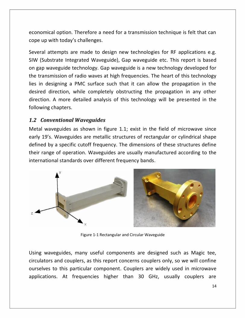
1.2 Conventional Waveguides
Metal waveguides as shown in figure 1.1; exist in the field of microwave since
early 19’s. Waveguides are metallic structures of rectangular or cylindrical shape
defined by a specific cutoff frequency. The dimensions of these structures define
their range of operation. Waveguides are usually manufactured according to the
international standards over different frequency bands.
Figure 1-1 Rectangular and Circular Waveguide
Using waveguides, many useful components are designed such as Magic tee,
circulators and couplers, as this report concerns couplers only, so we will confine
ourselves to this particular component. Couplers are widely used in microwave
applications. At frequencies higher than 30 GHz, usually couplers are

15
manufactured in two parts and later joined using screws. These couplers can work
up to 60GHz but to provide electrical contact and water proofing simultaneously
is not economical. Moreover, due to mechanical imperfections, electric field leaks
through them and thus degrades the performance. These problems are more
explained in the coming sections.
1.3 Design Specifications:
The purpose of this master thesis is to design a 3dB coupler using gap waveguide
technology around the center frequency of 38.5GHz for a bandwidth of 7%. The
proposed electrical specifications of the coupler are as follows:
Frequency Band 37-40 GHz
Coupling Required 3dB
Isolation -20dB
Input Matching -20dB
Waveguide Flange WR28
There were some proposed mechanical design requirements also, which will be
discussed in the last section of this thesis. Here we skip mechanical aspect of the
design for brevity.
1.4 Advantages expected from this Design:
The existing couplers are based on conventional waveguide technology. It’s a
hollow waveguide structure, which is broken into lid and ground plate such that
there is an electrical contact between these two components. Provision of a good
electrical contact between two side by side hollow waveguides is mechanically
difficult, due to the presence of thin wall between these two structures. On the

16
other hand, gap waveguides do not require any electrical contact between the
top lid and bottom plate. Therefore, a need was felt to utilize this unique feature
of gap waveguide technology.
Another difficulty with conventional technology was the requirement of
waterproofing of the structure. Water proofing is usually achieved by providing a
silicon layer at the edge of the waveguide. Electrical contact together with water
proofing poses some serious structural challenges. While gap waveguides provide
enough space for such water proofing requirements. One other advantage of gap
waveguides is that different transitions such as bends are easy to provide in gap
waveguides and still the structure can be planar.
This project is an attempt to encompass all these advantages and yet providing
promising performance.

17
2 Chapter 2
2.1 Couplers
Coupler is a four port passive device, which is used to couple the power from
input port to two out ports, while the fourth port is isolated. Figure 2-1 shows a
coupler with four ports, where port 1 is the input port, port 2 and 3 are the
output ports while port 4 is the isolated port. This device is completely symmetric,
therefore any port can be designated as input port and correspondingly the other
port combinations can be determined.
Figure 2-1 Ideal Coupler
18
These couplers are often called directional couplers due the fact that output ports
can only be assigned according to the input port. Power flows in a specific
direction, while no power is reflected back at any port. Therefore a directional
coupler is ideally matched at all ports. In RF literature, ports are normally named
for generalization. These port names are relative to the input port. For example,
in Figure one if we select port 1 as input port, then port 2 is through port, port 3 is
coupled port and port 4 is isolated port. Ideally all the power is divided between
through and coupled port while no power is available at isolated port. From here
onwards, ports will be referred by their names instead of numbers.
2.2 Performance Parameters
As performance measures, certain parameters are defined for couplers. These
parameters will be used during this report, so a brief definition is provided here.
For detailed definitions, reader can consult [19] .
2.2.1 Insertion Loss
Insertion loss is defined as the ratio between the power at input port and through
port. Insertion Loss is often expressed in dB.
2.2.2 Coupling Factor
Coupling factor is the amount of power coupled to the coupled port. It is often
defined as the ratio of incident power and coupled power. Coupling factor is also
expressed in dB.
2.2.3 Isolation
Isolation is defined as the ratio between the power at input and isolated ports. It
determines the power travelling in the backward direction. It is also expressed in
dB.
19
2.3 Types of Couplers:
Couplers can be divided mainly into two categories.
Forward Couplers
Backward Couplers
If the power is coupled at the coupled port then it is called a forward coupler,
similarly if the power is coupled to the isolated port then it is knows as backward
couplers. Of course the port names are interchanged in case of a backward
coupler. In this report we will focus on forward couplers. Backward couplers are
not much of interest for this report.
Couplers are implemented usually in waveguide or microstrip technologies.
Striplines are also used for couplers. Examples of microsrtip couplers are branch
line couplers, rate race etc. In waveguide technology, bethe-hole and short slot
couplers are widely used. This project is more concentrated on waveguide
technology, so we will not present microstrip couplers in detail.
2.3.1 Bethe-hole Coupler:
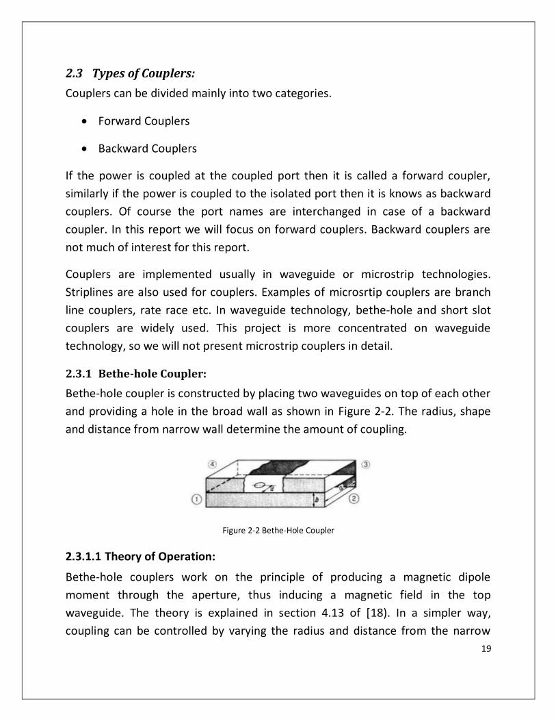
Bethe-hole coupler is constructed by placing two waveguides on top of each other
and providing a hole in the broad wall as shown in Figure 2-2. The radius, shape
and distance from narrow wall determine the amount of coupling.
Figure 2-2 Bethe-Hole Coupler
2.3.1.1 Theory of Operation:
Bethe-hole couplers work on the principle of producing a magnetic dipole
moment through the aperture, thus inducing a magnetic field in the top
waveguide. The theory is explained in section 4.13 of [18). In a simpler way,
coupling can be controlled by varying the radius and distance from the narrow

20
wall of the wave guide. It is assumed that the hole is located at centre of the
waveguide. Following formulas can be used to calculate the radius and location of
the hole.
In the above equations, ‘r’ is the radius of the hole, while ‘d’ is the distance from
the narrow wall. Also it is assumed that the guide walls are infinitely thin,
meaning that it’s having infinite conductivity.
The two wave guide not necessarily should be on top of each other, they can have
some angle θ as shown in Figure 3.
Figure 2-3 Bethe-hole coupler at an angle θ
Moreover, the hole needs not to be circular. The shape of the hole can be
rectangular or more commonly cross.
Another way for constructing the coupler is to add multiple holes, thus controlling
the amount of coupled power over a certain bandwidth is achieved. The holes are
quarter-wavelength apart and this produces zero transmission at port 4.
21
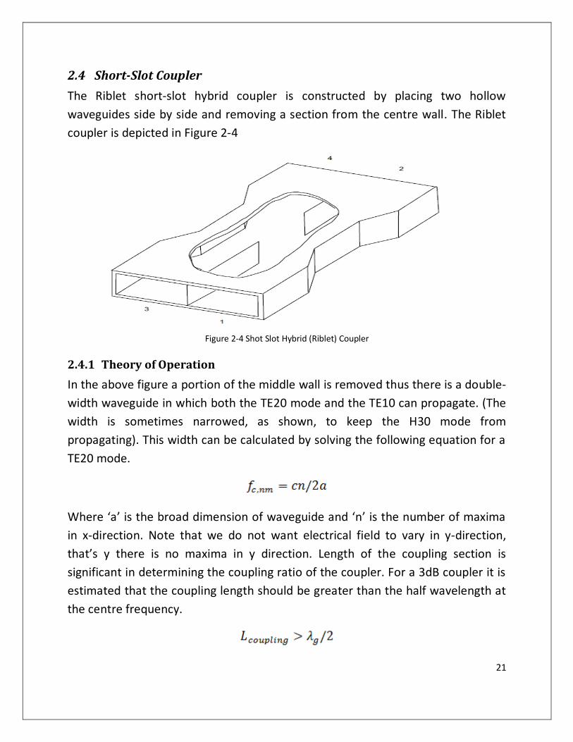
2.4 Short-Slot Coupler
The Riblet short-slot hybrid coupler is constructed by placing two hollow
waveguides side by side and removing a section from the centre wall. The Riblet
coupler is depicted in Figure 2-4
Figure 2-4 Shot Slot Hybrid (Riblet) Coupler
2.4.1 Theory of Operation
In the above figure a portion of the middle wall is removed thus there is a double-
width waveguide in which both the TE20 mode and the TE10 can propagate. (The
width is sometimes narrowed, as shown, to keep the H30 mode from
propagating). This width can be calculated by solving the following equation for a
TE20 mode.
Where ‘a’ is the broad dimension of waveguide and ‘n’ is the number of maxima
in x-direction. Note that we do not want electrical field to vary in y-direction,
that’s y there is no maxima in y direction. Length of the coupling section is
significant in determining the coupling ratio of the coupler. For a 3dB coupler it is
estimated that the coupling length should be greater than the half wavelength at
the centre frequency.
22
By choosing the length of the removed wall section properly, an equal division of
the power incident can be obtained with a good match at all ports. The forward-
going wave in the coupled guide has in addition a phase shift of 90 , whereas
there is no backward-going wave in the coupled guide. The theory of operation is
fully explained by Riblet [14] and [15]. In order to have a good match a capacitive
dome is provided in the middle of coupling section. The number of steps of
indentations determines the band width of the coupler. A wide band designed is
presented in [15 . his design u li es three indenta on sec ons with decreasing
lengths. iblet couplers usually provide a 9 phase shift that is the reason it is
known as hybrid coupler.
Another way of constructing the coupler is by providing the holes in the middle
wall. This type of arrangement resembles Bethe-hole. Such a design is difficult to
realize and cannot provide a good coupling for wider bandwidth [14].
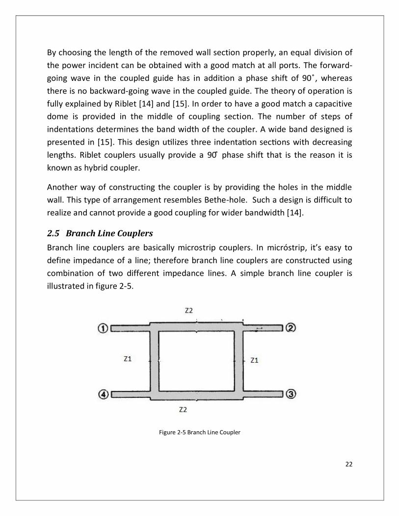
2.5 Branch Line Couplers
Branch line couplers are basically microstrip couplers. In micróstrip, it’s easy to
define impedance of a line; therefore branch line couplers are constructed using
combination of two different impedance lines. A simple branch line coupler is
illustrated in figure 2-5.
Figure 2-5 Branch Line Coupler

23
A branch line coupler uses quarter-wavelength lines with two different
impedances as shown in the above figure. The ratio between the impedance
depends on the amount of coupling required. A more detailed discussion can be
found in [18].
24
3 Chapter 3
3.1 Gap Waveguides
Hollow waveguides have been a medium for transmission of RF. Hollow
waveguides are metallic structures of any definite geometrical shape rectangle or
cylinder. The dimensions of these waveguides depend on the operation
frequency. These relations can be found in [18] and [19]. Hollow waveguides are
available from 3-80GHz, but more commonly they are used for 3-30GHz
transmission. They have the advantages of low loss and can withstand high
powers. On the other hand, when the frequency increases beyond 30GHz, the
dimensions become too small and difficult to realize in metal structures. Although
the microstrip structure is available for high frequencies, yet it has the additive
disadvantage of loss due to substrate. Therefore, a waveguide is more desirable
at high frequencies.

25
Many attempts have been made to overcome this problem of small dimensions in
waveguides. An example of which is SIW (substrate integrated waveguide). SIWs
are manufactured between two ground planes separated by a dielectric. Side
walls are provided using via-holes between two ground planes. This structure is
capable of supporting higher frequencies, yet the loss is high due to the
substrate involved.
3.2 Soft and Hard surfaces
The electromagnetic properties of a conducting surface can be altered by
incorporating a special texture on the surface which helps in describing the
surface with a single parameter termed as its surface impedance. Magnetic
conductivity does not exist naturally but can be realized in the form of high
surface impedance. The first conceptual attempt to realize high surface
impedance was the so called soft and hard surfaces [7], where they were defined
in terms of their anisotropic surface impedance.
Figure 3-1 Transversely Corrugated Soft Surface
Figure 3-1 describes a transversely corrugated soft surface with two principal
directions both being tangential to the surface: the longitudinal direction lˆ which
26
is in the direction of the pointing vector and the transverse direction tˆ
orthogonal to it. The longitudinal and transverse surface impedances are given by
From the knowledge of transversely corrugated surfaces we can uniquely define a
soft surface by
A grid of parallel PEC / PMC strips, where every second strip is PEC and PMC
respectively [3] is used now a day to describe the ideal soft and hard surfaces.
They are characterized by their anisotropic boundary conditions that allow an
arbitrary polarized wave to propagate along the strips (hard surface case)
whereas they stop wave propagation in directions orthogonal to the strips (soft
surface case). High impedance surfaces with a forbidden frequency band have
been discussed in detail in [8]. Due to the isotropic boundary conditions, the EBG
surface [8] stops wave propagation in all directions. Fakir's bed of nails refers to a
two dimensional array of metal pins [2] arranged on the conducting surface,
which mimic the ideal impedance surface boundary. It has been demonstrated in
[9], that by placing the structure in between two parallel plates and varying
different parameters typically the gap height, can produce extremely large band
gap (parallel plate stop band)(2.5:1) to prevent wave propagation. The surface
impedance is very high in the band gap, so the tangential magnetic field is small,
even with a large electric field along the surface. Such a structure is sometimes
described as a magnetic conductor.
3.3 PMC Realization using bed of nails
In fact there are many ways of realizing parallel plate stop band, which have been
compared in [10], but gap waveguides introduced in [1] and experimentally
verified by use of bed of nails [2], as a high impedance surface for parallel plate
27
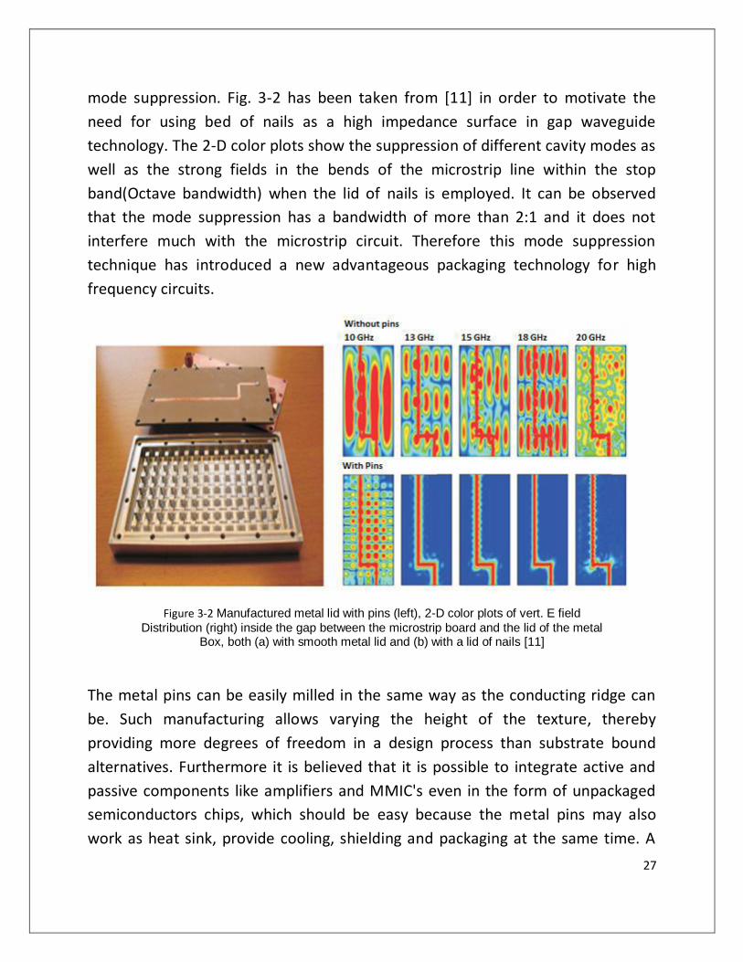
mode suppression. Fig. 3-2 has been taken from [11] in order to motivate the
need for using bed of nails as a high impedance surface in gap waveguide
technology. The 2-D color plots show the suppression of different cavity modes as
well as the strong fields in the bends of the microstrip line within the stop
band(Octave bandwidth) when the lid of nails is employed. It can be observed
that the mode suppression has a bandwidth of more than 2:1 and it does not
interfere much with the microstrip circuit. Therefore this mode suppression
technique has introduced a new advantageous packaging technology for high
frequency circuits.
Figure 3-2 Manufactured metal lid with pins (left), 2-D color plots of vert. E field Distribution (right) inside the gap between the microstrip board and the lid of the metal
Box, both (a) with smooth metal lid and (b) with a lid of nails [11]
The metal pins can be easily milled in the same way as the conducting ridge can
be. Such manufacturing allows varying the height of the texture, thereby
providing more degrees of freedom in a design process than substrate bound
alternatives. Furthermore it is believed that it is possible to integrate active and
passive components like amplifiers and MMIC's even in the form of unpackaged
semiconductors chips, which should be easy because the metal pins may also
work as heat sink, provide cooling, shielding and packaging at the same time. A
28
comparative study for investigating the PMC realizations[10], has motivated the
need to use bed of nails approach, providing band stop for more than an octave
band, furthermore this technology is having less loss, cheap and easy to mill.
3.4 Waveguide Implementation using High Impedance surface
In the above explained bed of nails, we can alter the structure in such a way that
only a desired frequency can propagate and rest of the frequencies is stopped.
Two types of approaches are implemented:
Ridge Gap waveguide
Groove Gap waveguide
Both of these techniques are explained in the sections below.
3.4.1 Ridge Gap waveguide
The propagation characteristics along soft and hard surfaces are very well known,
either when they are introduced in hollow waveguides or as open hard and soft
surfaces. [3]. The detection of local surface waves along each groove of a hard
surface, introduced in[12], has been followed by the detection of local modes
along the ridges of a longitudinal corrugated hard surface, when a smooth metal
plate, separated by a narrow gap was located over it[13]. This has resulted in a
new way of killing higher order modes [13], by introducing the hard surface in a
TEM parallel-plate waveguide. The geometry in [13] has been simplified and
improved in [1] to introduce a new basic waveguide confined in the gap between
parallel plates.
3.4.1.1 Principle of Operation
The principle of operation of the gap waveguide is based on the following
theoretical facts that are either well known or can readily be derived from
Maxwell's equations
If the gap height 'h' between a PEC and a PMC surface is less than a quarter
wavelength, the wave propagation becomes prohibited in any arbitrary
direction.
29
Wave propagation in any direction can be made prohibited, in between a
PEC and an EBG surface if the gap height is typically small. This gap height
depends upon the geometry of the EBG surface and it is found to be less
than a quarter wavelength as well. The PEC boundary conditions between
the parallel plates for horizontal polarization provides cut-off whenever h <
λ/2, which is a weaker cut-off condition than h < λ/4, which is valid for the
PMC boundary condition on the lower plate.
Waves in the gap between a PEC surface and a PEC/PMC strip grid can only
propagate along the direction of the PEC strips whereas they are in cut-off
for vertical(TM) and horizontal (TE) polarization when h < λ/4 and h < λ/2
respectively. Therefore an ideal gap waveguide works for all frequencies
up to a maximum defined by h = λ/4.
The bandwidth of the propagating wave along the ridge can be estimated from
the frequency band over which the propagation constant in directions away from
the ridge is imaginary, corresponding to an evanescent wave. For the special bed
of nails EBG surface used in [1], the PMC appears ideal for thin pins and small
periods when the pin length d = λ/4 and the band gap is at high frequency limited
by a TE wave starting to propagate when d+h = λ/2. From the comparative studies
of [10], it was possible to design gap waveguides with octave bandwidth (2:1).
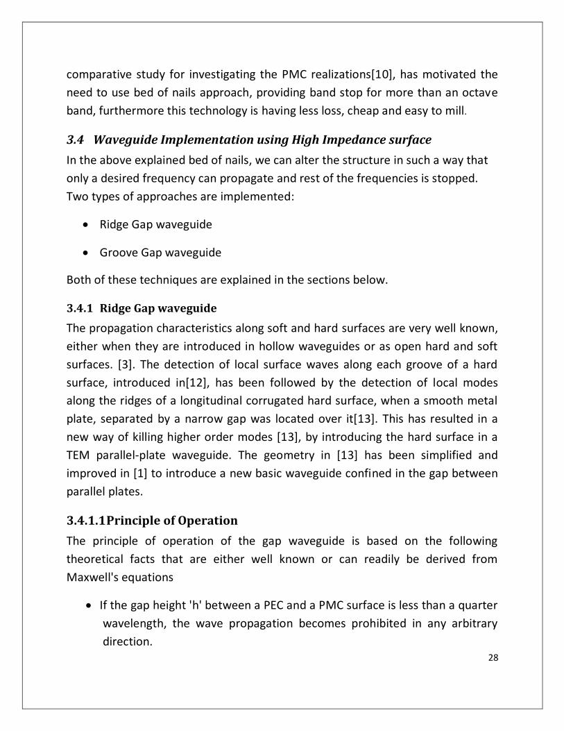
Figure 3-3 has been taken from [1] showing the dispersion diagrams for the gap
waveguide to justify the above discussion related to its band stop characteristics.
The dispersion diagrams in Figure 3-3(a) and Figure 3-3(b) were computed
without ridges for infinite periodic structure and finite dimensions in transverse
plane with PEC side walls respectively, showing a large stop band above 10 GHz
where no waves can propagate. The basic parallel plate mode that started at zero
frequency as a TEM mode is represented by the left curve in Figure 3-3 (a). This
mode is then deviated from the light line and went into cut-off just below 10 GHz.
It appeared again at 23 GHz together with another mode. Several rectangular
waveguide modes appeared below 10GHz, when metal walls were introduced,
limiting the transverse extent of the parallel plate geometry in Figure 3-3 (b).
These modes have a lower cut-off similar to normal rectangular waveguide modes
30
but went into a stop band just below 10 GHz and appeared again at the end of
this parallel plate stop band at 21 GHz. The dispersion diagram of Figure 3-3(c)
includes the ridge as well. The diagram which relates the introduction of the ridge
shows a new mode propagating closely to the light line, in fact following the ridge
within the whole parallel plate stop band. This is the desired quasi-TEM mode and
it is termed as quasi-TEM because it follows the light line very closely but not
exactly. Another higher order gap waveguide mode appeared at 19 GHz, having a
vertical E field distribution with asymmetrical sinusoidal dependence across the
ridge, being zero in the middle of the ridge.
(a) Infinite pin structure (b) Finite pin structure with PEC side walls
Figure 3-3 Dispersion diagram for the gap waveguide [1]
3.4.2 Groove Gap Waveguide
The groove gap waveguide is designed on the same principle as explained in the
above sections. Its uses the same high impedance surface (bed of nails) to
31
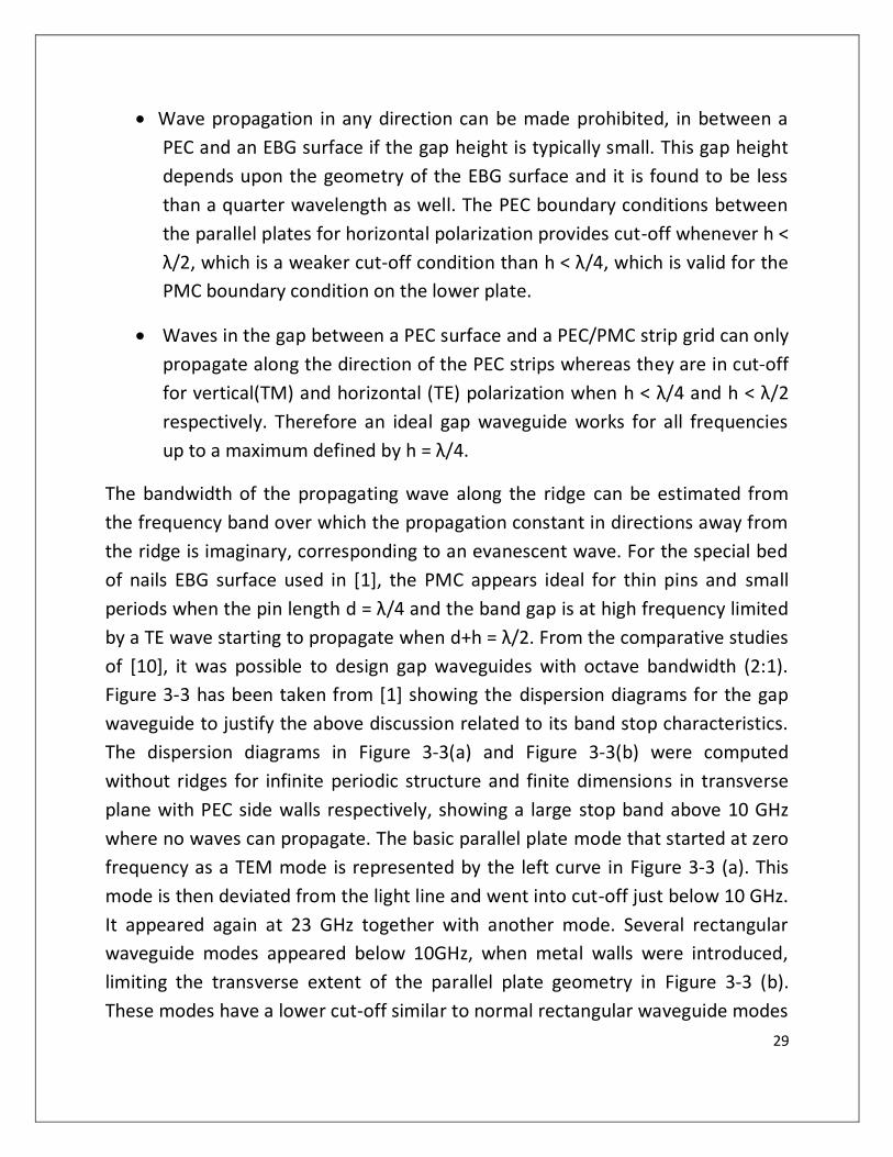
implement EBG concept. The difference between ridge and groove gap wave
guide is that in groove gap waveguide field propagates in the interior of a groove
created in the textured surface instead of along the top of a ridge [13]. The
boundary conditions for the field in the groove are the ones given by four metal
walls, but with the equivalent of a magnetic conducting strip in each of the
corners between the upper horizontal plate and the two vertical metal walls.
Consequently, the groove is expected to allow the propagation of modes in a
similar way as in hollow rectangular waveguides, i.e., with a cutoff frequency
given by the groove dimensions. Due to these similarities, this groove can also
potentially be used to design horn antennas radiating from apertures between
the two contactless parallel plates. It would be advantageous if such horns could
radiate two polarizations (perpendicular and parallel to the plates, referred to as
vertical and horizontal polarizations, respectively),
(a) Vertical Polarization
(b) Horizontal Polarization
Figure 3-4 Cross-sections of the groove gap waveguide for vertical and horizontal Polarizations for vertical and
horizontal polarizations. The grey areas are metal Pins (periodic along z-axis), and the black areas solid metal[14]
3.4.2.1 Principle of Operation
Groove gap waveguide is an alternate of rectangular hollow waveguide. It can
support TE and TM modes. The dimension of the groove determines the cutoff
frequency, guided wavelength and propagation constant. We can easily apply all
the formulas of rectangular hollow waveguides to groove gap waveguides.
32
(a) Horizontal groove (b) Vertical groove
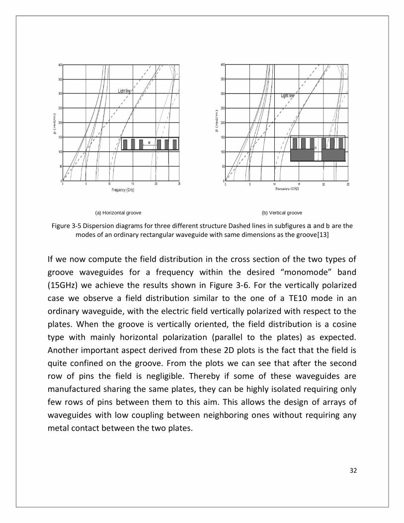
Figure 3-5 Dispersion diagrams for three different structure Dashed lines in subfigures a and b are the modes of an ordinary rectangular waveguide with same dimensions as the groove[13]
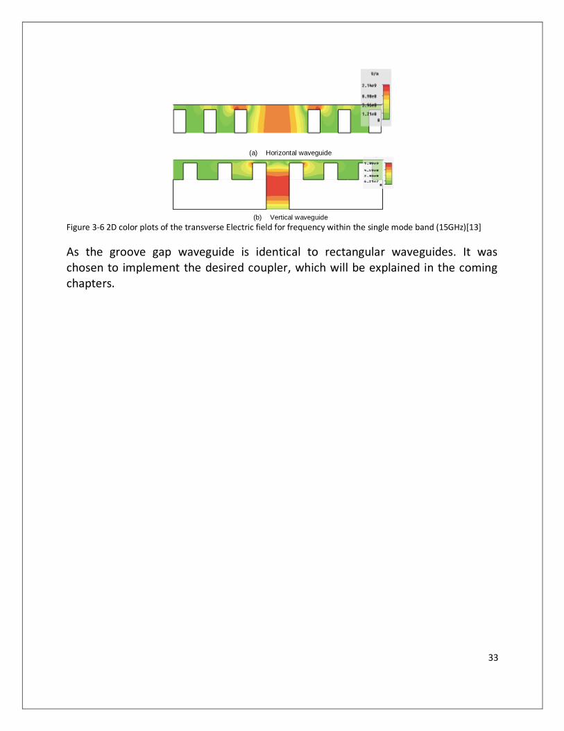
If we now compute the field distribution in the cross section of the two types of
groove waveguides for a frequency within the desired “monomode” band
(15GHz) we achieve the results shown in Figure 3-6. For the vertically polarized
case we observe a field distribution similar to the one of a TE10 mode in an
ordinary waveguide, with the electric field vertically polarized with respect to the
plates. When the groove is vertically oriented, the field distribution is a cosine
type with mainly horizontal polarization (parallel to the plates) as expected.
Another important aspect derived from these 2D plots is the fact that the field is
quite confined on the groove. From the plots we can see that after the second
row of pins the field is negligible. Thereby if some of these waveguides are
manufactured sharing the same plates, they can be highly isolated requiring only
few rows of pins between them to this aim. This allows the design of arrays of
waveguides with low coupling between neighboring ones without requiring any
metal contact between the two plates.
33
(a) Horizontal waveguide
(b) Vertical waveguide
Figure 3-6 2D color plots of the transverse Electric field for frequency within the single mode band (15GHz)[13]
As the groove gap waveguide is identical to rectangular waveguides. It was chosen to implement the desired coupler, which will be explained in the coming chapters.

34
4 Chapter 4
4.1 Coupler Design and Simulation
So far we have explained the technology and concept required to design the
coupler. In this chapter we will layout the actual design procedure and the
theoretical basis to proceed in future. All the simulations were performed in HFSS
v12.0. The initial design was implemented without taking into account the size
and measurements consideration. The final design of the coupler will be
explained in chapter 5.

35
4.2 Groove Gap waveguide Implementation
The first step is to implement the concepts explained in chapter 3 in HFSS. As we
know that gap waveguides can be implemented in two ways as explained earlier.
Therefore it was possible to proceed with any technology (i-e ridge or groove).
We have chosen groove gap waveguide due to the fact that Arkivator is having
the current design implemented in rectangular hollow waveguides. As groove
wave guides are identical to rectangular waveguides, it will be easy to compare
the results for both of the designs. Moreover, in groove gap waveguide, we need
not to design transitions (i-e from rectangular waveguide to Ridge waveguide and
vice versa). Therefore Groove waveguide was chosen due its simplicity and ease
of manufacturing.
The groove waveguide was implemented first by using the dimension given in
[reference]. Following are the dimensions used for initial Groove
waveguidedesign.
Pin Size(mm) Groove Width(mm) Air Gap(mm) Pin Period(mm)
WG Length (mm) Material
3×3×5 15.8 1 4 45 Copper Table 1
Figure 4-1 Cross-section of Groove waveguuide
Although it is established in chapter 3, that 2 rows of pins on both side of groove is enough but we have used 3 rows, in order to provide good isolation in case of an adjacent waveguide. The simulated results for this structure are presented in Figure 4-2.
Groove Width Air Gap
Pin Period
36
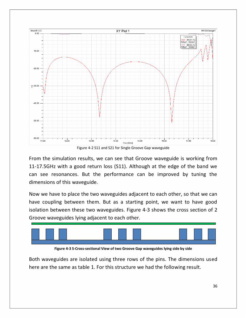
Figure 4-2 S11 and S21 for Single Groove Gap waveguide
From the simulation results, we can see that Groove waveguide is working from
11-17.5GHz with a good return loss (S11). Although at the edge of the band we
can see resonances. But the performance can be improved by tuning the
dimensions of this waveguide.
Now we have to place the two waveguides adjacent to each other, so that we can
have coupling between them. But as a starting point, we want to have good
isolation between these two waveguides. Figure 4-3 shows the cross section of 2
Groove waveguides lying adjacent to each other.
Figure 4-3 S-Cross-sectional View of two Groove Gap waveguides lying side by side
Both waveguides are isolated using three rows of the pins. The dimensions used
here are the same as table 1. For this structure we had the following result.

37
Figure 4-4 S-Parameters for two Groove Gap waveguides lying side by side
From Figure 4-4, it is evident that isolation between two waveguides is less than -
30dB over the entire band. Therefore, it is possible to place two waveguides side
by side and yet can have a good isolation.
The above mentioned simulation was meant only for 11-18GHz. In order to move
to our desired frequency band, we need to scale down the dimensions so that
waveguide can work in the band of 37-40 GHz. Following are the dimensions
chosen for our groove waveguide.
Pin Size(mm) Groove Width(mm) Air Gap(mm) Pin Period(mm)
WAVEGUIDE Length (mm) Material
0.62×0.62×2.06 6.539 0.413 1.03 45 Copper Table 2
Table 2 gives the values which will provide the best results in our desired band.
We can observe that all the values are not exact multiples of the values of table 1.
The reason is that we have tuned the dimensions in such a way that we can have
38
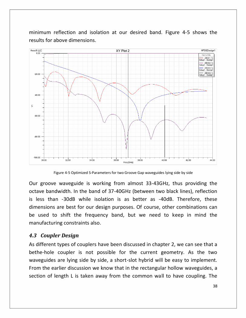
minimum reflection and isolation at our desired band. Figure 4-5 shows the
results for above dimensions.
Figure 4-5 Optimized S-Parameters for two Groove Gap waveguides lying side by side
Our groove waveguide is working from almost 33-43GHz, thus providing the
octave bandwidth. In the band of 37-40GHz (between two black lines), reflection
is less than -30dB while isolation is as better as -40dB. Therefore, these
dimensions are best for our design purposes. Of course, other combinations can
be used to shift the frequency band, but we need to keep in mind the
manufacturing constraints also.
4.3 Coupler Design
As different types of couplers have been discussed in chapter 2, we can see that a
bethe-hole coupler is not possible for the current geometry. As the two
waveguides are lying side by side, a short-slot hybrid will be easy to implement.
From the earlier discussion we know that in the rectangular hollow waveguides, a
section of length L is taken away from the common wall to have coupling. The
39
thickness of this wall is assumed to be zero for ideal case. In the case of gap
waveguide, common wall is the middle three rows Figure 4-3, and we cannot
assume it to be zero thickness. Another alternative can be removing one row of
the pins, as two rows can provide good isolation. Moreover, the two rows of the
dimensions of table 2, constitutes a quarter wavelength distance, which can
reduce the effect of reflection of the coupling section.
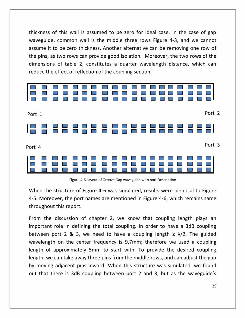
Figure 4-6 Layout of Groove Gap waveguide with port Description
When the structure of Figure 4-6 was simulated, results were identical to Figure
4-5. Moreover, the port names are mentioned in Figure 4-6, which remains same
throughout this report.
From the discussion of chapter 2, we know that coupling length plays an
important role in defining the total coupling. In order to have a 3dB coupling
between port 2 & 3, we need to have a coupling length ≥ λ/2. he guided
wavelength on the center frequency is 9.7mm; therefore we used a coupling
length of approximately 5mm to start with. To provide the desired coupling
length, we can take away three pins from the middle rows, and can adjust the gap
by moving adjacent pins inward. When this structure was simulated, we found
out that there is 3dB coupling between port 2 and 3, but as the waveguide’s
Port 1 Port 2
Port 4 Port 3

40
broad dimension is doubled at the coupling section, it causes a big mismatch at
port 1. Moreover, the 3dB coupling is not in our desired frequency range. This
frequency shift can be adjusted by the length of the coupling section. In order to
compensate the width, we know from chapter 2, that indentations are provided
in rectangular waveguides, to match the phase of higher order odd modes (TE20).
A similar indentation is provided for our structure and also the coupling length is
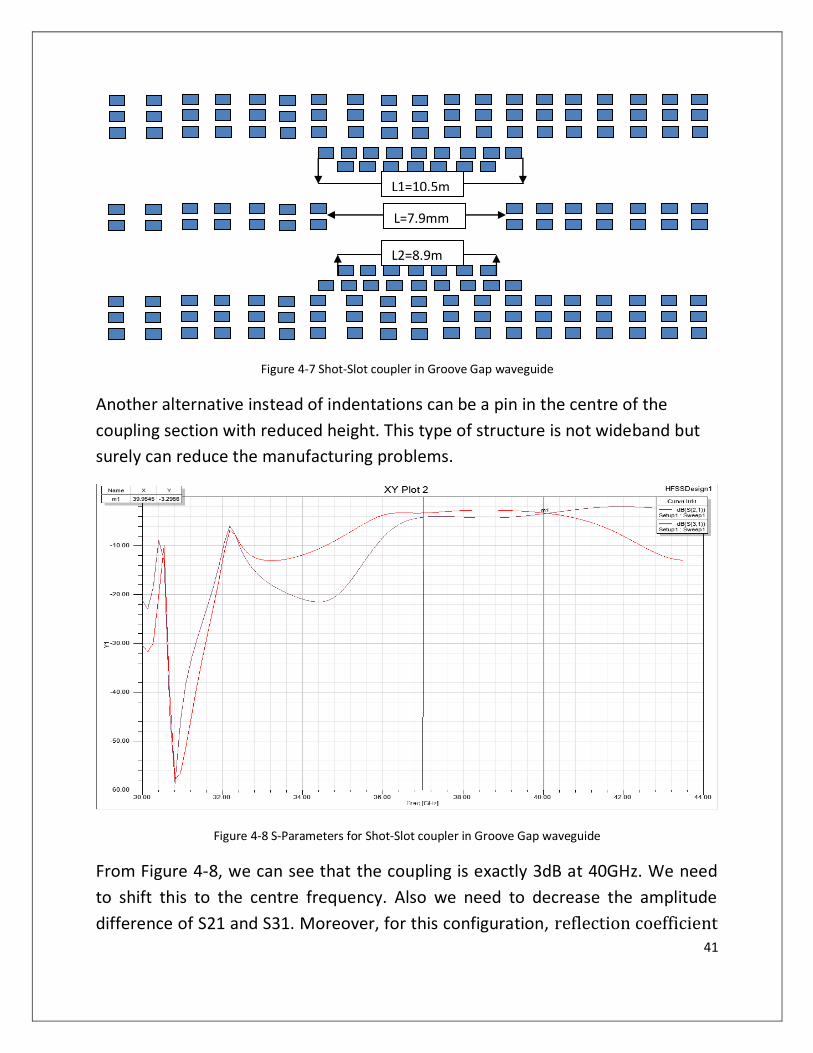
tuned in Figure 4-7. The indentations were provided by adding extra pins to the
side walls of coupling section as shown in figure 4-7. For a start, a single row of
pins slightly greater than the coupling length was introduced (L1 in Figure 4-7).
Then this row was displaced towards the coupling section, keeping in mind that it
should not reach the centre of the guide, as a pin in the center of the guide can
block the propagation. When the distance of this extra row from the side wall
exceeded the normal period of pins, an intermediate section was provided. This
intermediate section is denoted as L1 in Figure 4-7. Such indentation sections can
be added further to improve the bandwidth. But the distance between the pins
gets too small and difficult to realize. The displacement from the sidewall is found
analytically. Another alternative instead of indentations can be a pin in the centre
of the coupling section with reduced height. This type of structure is not
wideband but surely can reduce the manufacturing problems.
41
Figure 4-7 Shot-Slot coupler in Groove Gap waveguide
Another alternative instead of indentations can be a pin in the centre of the
coupling section with reduced height. This type of structure is not wideband but
surely can reduce the manufacturing problems.
Figure 4-8 S-Parameters for Shot-Slot coupler in Groove Gap waveguide
From Figure 4-8, we can see that the coupling is exactly 3dB at 40GHz. We need
to shift this to the centre frequency. Also we need to decrease the amplitude
difference of S21 and S31. Moreover, for this configuration, reflection coefficient
L=7.9mm
L1=10.5m
m
L2=8.9m
m
42
and return loss is -15dB. In order to improve all these factors, various techniques
can be applied. For example, we can have two extra pins, at the start and end of
the coupling sections for a good match, but it was noticed that it increases the
amplitude difference. Length of the indentations is also important and the width
of the waveguide in the coupling section determines the amplitude difference. To
control all these factors we have introduced pucks in the waveguide, which is
explained in the following section.
4.4 Matching
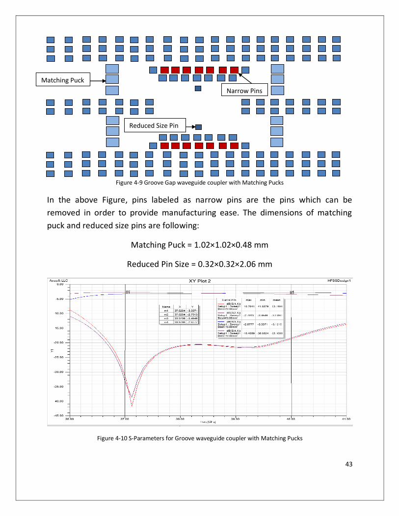
Introducing the puck in a rectangular WG means that floor of the WG is made
uneven on the selected place. These pucks can be viewed as matching stubs in
microstrip structures. The similar can be provided for groove WG. We have
introduced pins with reduced height and increased size before and after the
indentations. These pins act as a phase balancer for odd mode and also provide a
good match at all ports. Positions for these pins were determined by parametric
sweep along the length of the waveguide. It was noticed that the height of these
pins should be ≤ half of the height of the normal pin, because if we introduce a
pin of the same height in the waveguide, it ceases the transmission. Simulation
was tried with different number of pins. The best results were obtained by
introducing twelve such pins at the four ports. Also the coupling length was
optimized for our frequency band. To reduce the amplitude difference, a reduced
size pins were provided in the middle of indentation, thus it makes the phase of
even and odd mode equal and provides a good coupling. The final structure is
given in Figure 4-9
43
Figure 4-9 Groove Gap waveguide coupler with Matching Pucks
In the above Figure, pins labeled as narrow pins are the pins which can be
removed in order to provide manufacturing ease. The dimensions of matching
puck and reduced size pins are following:
Matching Puck = 1.02×1.02×0.48 mm
Reduced Pin Size = 0.32×0.32×2.06 mm
Figure 4-10 S-Parameters for Groove waveguide coupler with Matching Pucks
Matching Puck
Reduced Size Pin
Narrow Pins

44
Figure 4.11 shows the final results for the coupler design. We can see that the
reflection and isolation is ≤-20dB over the entire band. The amplitude maximum
difference is 0.5dB. Although the phase difference was not included in the
specifications, yet we can plot the phase difference of S21 and S31.
It was also observed that the phase difference is 9 over the en re band. o we
can safely say that the above designed coupler is a 9 hybrid coupler with a
bandwidth ≥7.5%-
45
5 Chapter 5
5.1 Mechanical Considerations
In this chapter, mechanical aspects of the design are considered. As the gap
waveguide is a new technology, and measurement techniques are not developed
for these waveguides. To be able to measure using conventional methods, we
need to have standard rectangular waveguide ports. For mounting these ports,
bends are also required. Finally the limitation of milling is also considered. In
short we need to transform our design, in such a way that it can interface with
existing Microwave Techniques.

46
5.2 Mechanical Problems
The design presented in chapter 4 is having few mechanical issues. These can be
divided into two categories.
Interface Problems
Milling Problems
In order to measure the performance of our coupler, we need to address both of
these issues separately.
5.3 Interface Problems
Gap waveguide is a newly developed technology. In order to be used with
conventional microwave equipment, we need to interface Gap waveguide with
rectangular standard ports. All the rectangular waveguides are manufactured
according to international standards. This implies that their dimensions must be
of a standard size. When we were designing the coupler, we have not taken in to
account the dimensions; rather we have just scaled down the dimensions to get
the desired result. If we recall the dimensions of our waveguide from chapter 4,
we can easily see that we are shorter than the WR28 dimensions, which is a
standard waveguide for this frequency band. Our current dimension is
6.539×2.468mm while the standard waveguide is having the dimension of
7.11×3.56mm.
Another important thing is that the distance between the two waveguides is too
small. Therefore, a waveguide ange cannot be mounted using this small
distance. We need to turn all the ports by 9 , in order to mount a standard
flange. Design for bends is discussed in the following sections.

47
5.3.1 Waveguide Bends
Waveguide bends are characterized as E plane and H plane bends. E plane bends
are used when we want to move from a horizontal waveguide to a vertical
waveguide such as bethe-hole. In H plane design, bend is introduced in the same
plane for both waveguides. As our waveguides are side by side, therefore we
need an H plane bend.
H plane bends can be implemented in different ways as discussed in [16 . We
have used the cross bend technique to implement 9 bend as shown in Figure 5.1
Figure 5-1 Cross H Plane bend for Rectangular waveguide
In the above Figure, two rectangular waveguides are connected using an H plane
cross bend. The dimension of the cross W and L determines the bandwidth of the
waveguide. The dimensions of waveguides were kept similar to Gap waveguide.
Simulated results are plotted in Figure 5.2
48
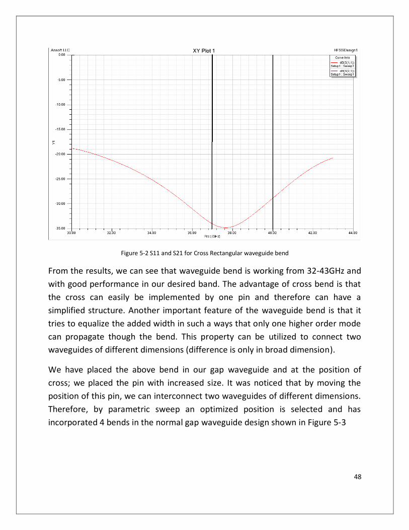
Figure 5-2 S11 and S21 for Cross Rectangular waveguide bend
From the results, we can see that waveguide bend is working from 32-43GHz and
with good performance in our desired band. The advantage of cross bend is that
the cross can easily be implemented by one pin and therefore can have a
simplified structure. Another important feature of the waveguide bend is that it
tries to equalize the added width in such a ways that only one higher order mode
can propagate though the bend. This property can be utilized to connect two
waveguides of different dimensions (difference is only in broad dimension).
We have placed the above bend in our gap waveguide and at the position of
cross; we placed the pin with increased size. It was noticed that by moving the
position of this pin, we can interconnect two waveguides of different dimensions.
Therefore, by parametric sweep an optimized position is selected and has
incorporated 4 bends in the normal gap waveguide design shown in Figure 5-3
49
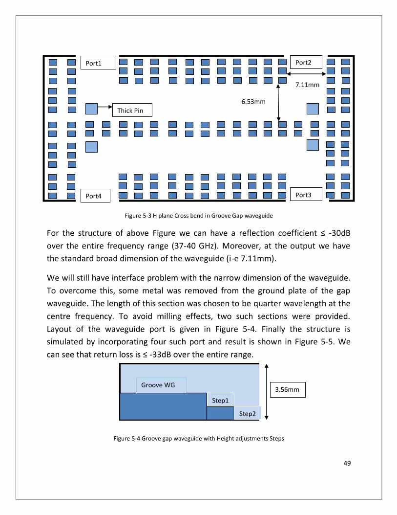
Figure 5-3 H plane Cross bend in Groove Gap waveguide
For the structure of above Figure we can have a reflection coefficient ≤ -30dB
over the entire frequency range (37-40 GHz). Moreover, at the output we have
the standard broad dimension of the waveguide (i-e 7.11mm).
We will still have interface problem with the narrow dimension of the waveguide.
To overcome this, some metal was removed from the ground plate of the gap
waveguide. The length of this section was chosen to be quarter wavelength at the
centre frequency. To avoid milling effects, two such sections were provided.
Layout of the waveguide port is given in Figure 5-4. Finally the structure is
simulated by incorporating four such port and result is shown in Figure 5-5. We
can see that return loss is ≤ -33dB over the entire range.
Figure 5-4 Groove gap waveguide with Height adjustments Steps
Thick Pin
7.11mm
6.53mm
Port1
Port2
Port4
44444
44
Port3
Groove WG
Step1
3.56mm
Step2
50
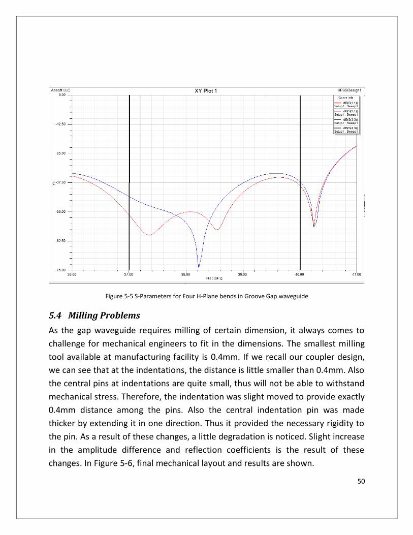
Figure 5-5 S-Parameters for Four H-Plane bends in Groove Gap waveguide
5.4 Milling Problems
As the gap waveguide requires milling of certain dimension, it always comes to
challenge for mechanical engineers to fit in the dimensions. The smallest milling
tool available at manufacturing facility is 0.4mm. If we recall our coupler design,
we can see that at the indentations, the distance is little smaller than 0.4mm. Also
the central pins at indentations are quite small, thus will not be able to withstand
mechanical stress. Therefore, the indentation was slight moved to provide exactly
0.4mm distance among the pins. Also the central indentation pin was made
thicker by extending it in one direction. Thus it provided the necessary rigidity to
the pin. As a result of these changes, a little degradation is noticed. Slight increase
in the amplitude difference and reflection coefficients is the result of these
changes. In Figure 5-6, final mechanical layout and results are shown.
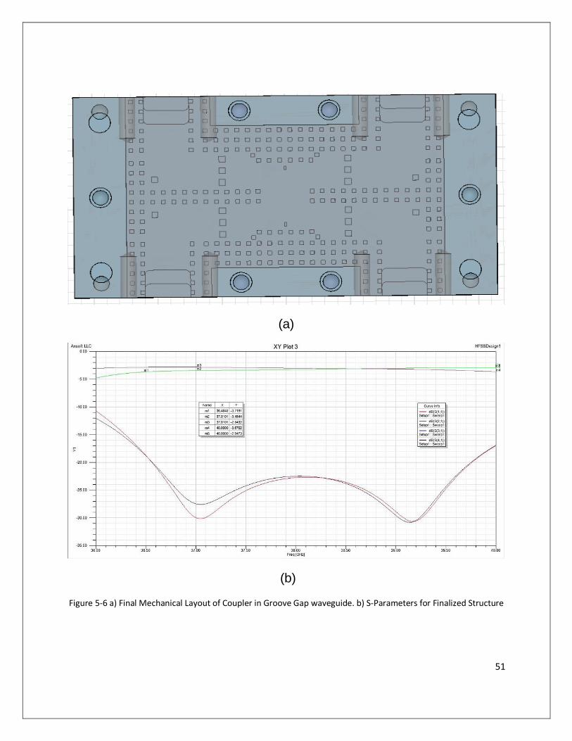
51
(a)
(b)
Figure 5-6 a) Final Mechanical Layout of Coupler in Groove Gap waveguide. b) S-Parameters for Finalized Structure

52
6 Chapter 6
6.1 Measurements and Conclusions
This chapter contains the measurement results and the conclusions drawn from
those measurements. All the measurements were performed at Antenna
department, Chalmers University of Technology. For measurements, we have
used standard WR 28 calibration kit with Vector Network Analyzer (). For plotting
and comparison, matlab was used as a plotting platform. Matlab codes can be
accessed in appendix.
6.2 Calibration of VNA
Before performing the measurements, VNA was calibrated using TRL calibration.
For this calibration, standard calibration kit for WR 28 rectangular waveguide was
used. After the calibration, it was noted that return loss was less than -40dB for
53
standard through transmission. Moreover, the frequency range selected for
measurement was 30-40GHz. As it is mentioned before that our designed gap
waveguide works in the range of 30-43 GHz.
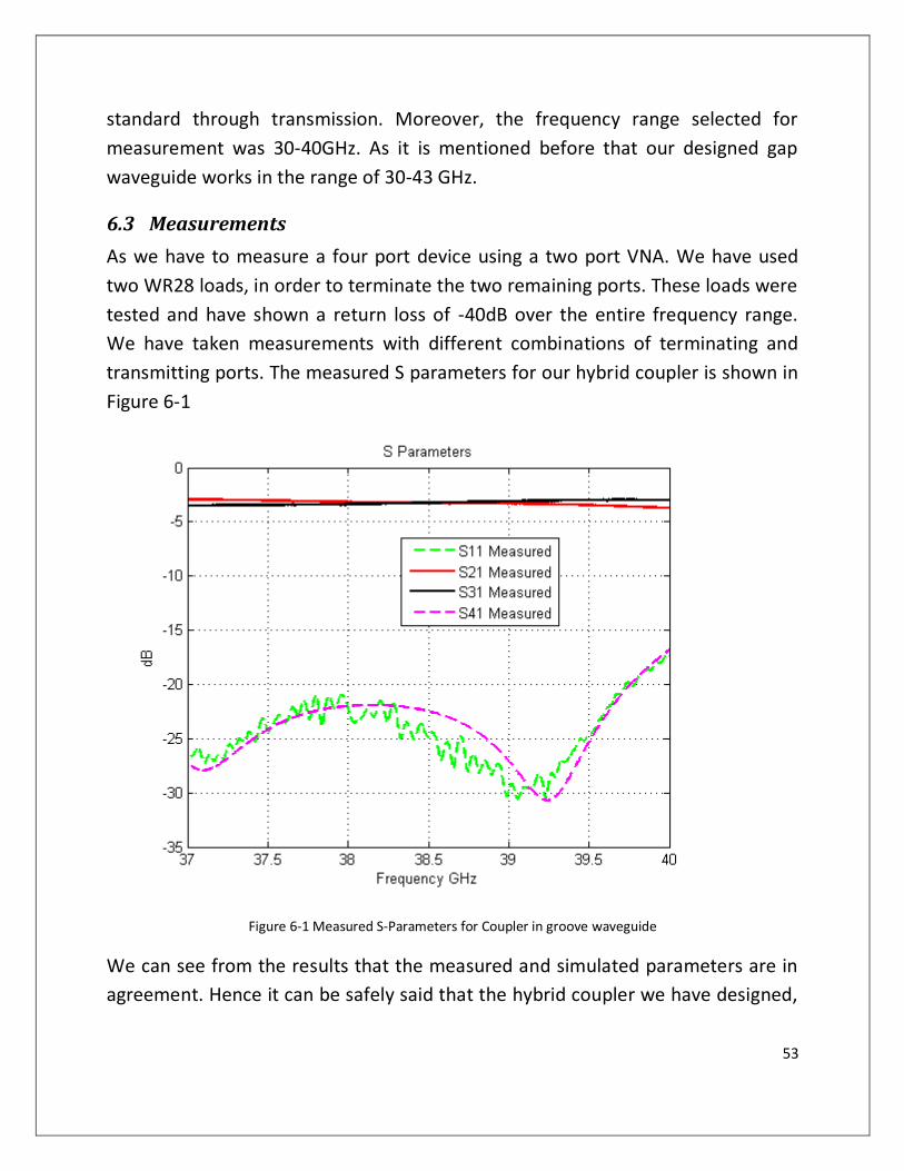
6.3 Measurements
As we have to measure a four port device using a two port VNA. We have used
two WR28 loads, in order to terminate the two remaining ports. These loads were
tested and have shown a return loss of -40dB over the entire frequency range.
We have taken measurements with different combinations of terminating and
transmitting ports. The measured S parameters for our hybrid coupler is shown in
Figure 6-1
Figure 6-1 Measured S-Parameters for Coupler in groove waveguide
We can see from the results that the measured and simulated parameters are in
agreement. Hence it can be safely said that the hybrid coupler we have designed,
54
can work in the range of 37-40 GHz. A more detailed analysis of these
measurements was made in the coming sections.
6.4 Analysis
Analysis of results can be divided into following categories.
Amplitude Analysis
Phase Analysis
Wide Band Analysis
The measurements are analyzed over the range of 37-40 GHz; it is our desired
frequency range as mentioned in chapter 1. Finally a wide band analysis is
performed in order to estimate the percentage bandwidth of the this hybrid
coupler.
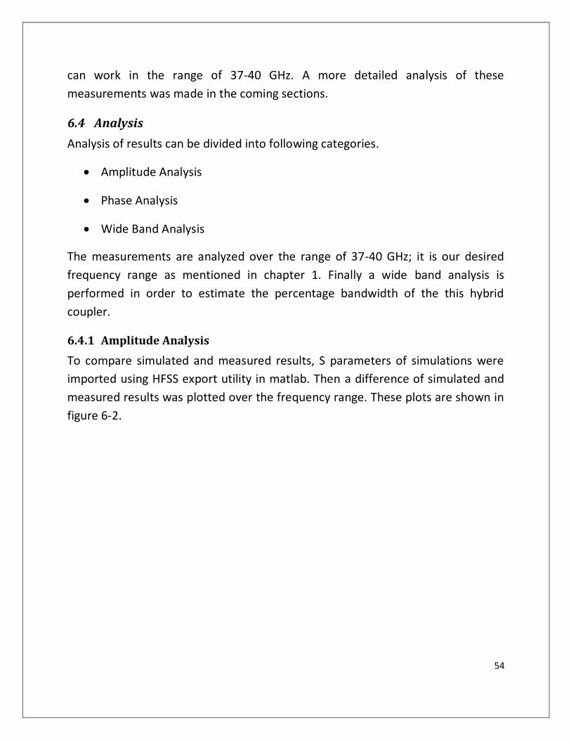
6.4.1 Amplitude Analysis
To compare simulated and measured results, S parameters of simulations were
imported using HFSS export utility in matlab. Then a difference of simulated and
measured results was plotted over the frequency range. These plots are shown in
figure 6-2.
55
Figure 6-2 Amplitude Difference between Measure and Simulated Results
From figure 6-2 as we can see that the amplitude difference between measured
and simulated values is in the range of ±0.04dB. Amplitude difference is
calculated by subtracting S21 and S31 (both in dB for measure and simulated
results). S11 shows a rippled plot. The reason is that calibration of short in TRL
was not performed accurately, therefore the response in not smooth for S11.
Therefore, we have plotted an absolute difference between measured and
simulated results. The absolute difference is calculated by subtracting the S-
parameters (measured and simulated) and then taking the absolute value for this
complex difference, finally the values are expressed in dB. We can see that for S11
and S41 the absolute difference is some what below -30dB. By this analysis, we
can safely say that the amplitude of all S parameters meet the design
requirements. Although the return loss for 40GHz is a little high, yet it was the
same in simulation results.
6.4.2 Phase Analysis
The exact phase of S21 and S31 is not easy to determine from Measured S
parameters, As it involves the complex phase unwrapping algorithms. But we can
find the phase difference of coupled and though port. As the measurements were
56
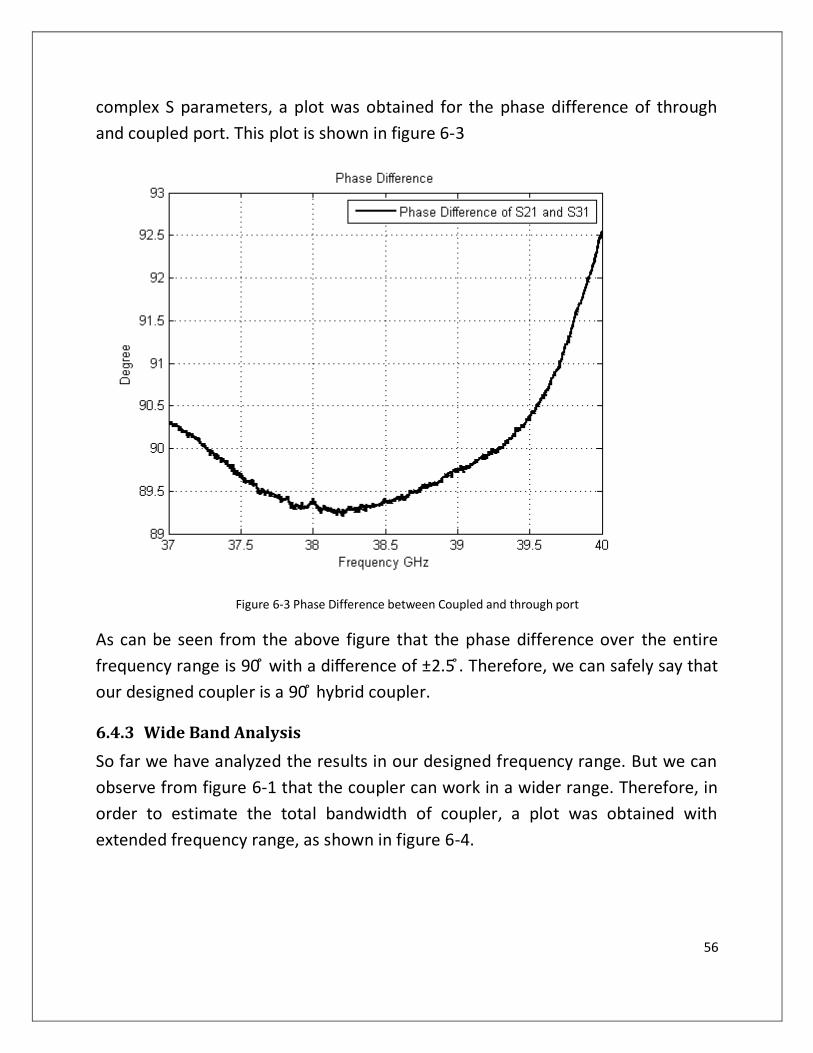
complex S parameters, a plot was obtained for the phase difference of through
and coupled port. This plot is shown in figure 6-3
Figure 6-3 Phase Difference between Coupled and through port
As can be seen from the above figure that the phase difference over the entire
frequency range is 9 with a di erence of 2.5 . herefore, we can safely say that
our designed coupler is a 9 hybrid coupler.
6.4.3 Wide Band Analysis
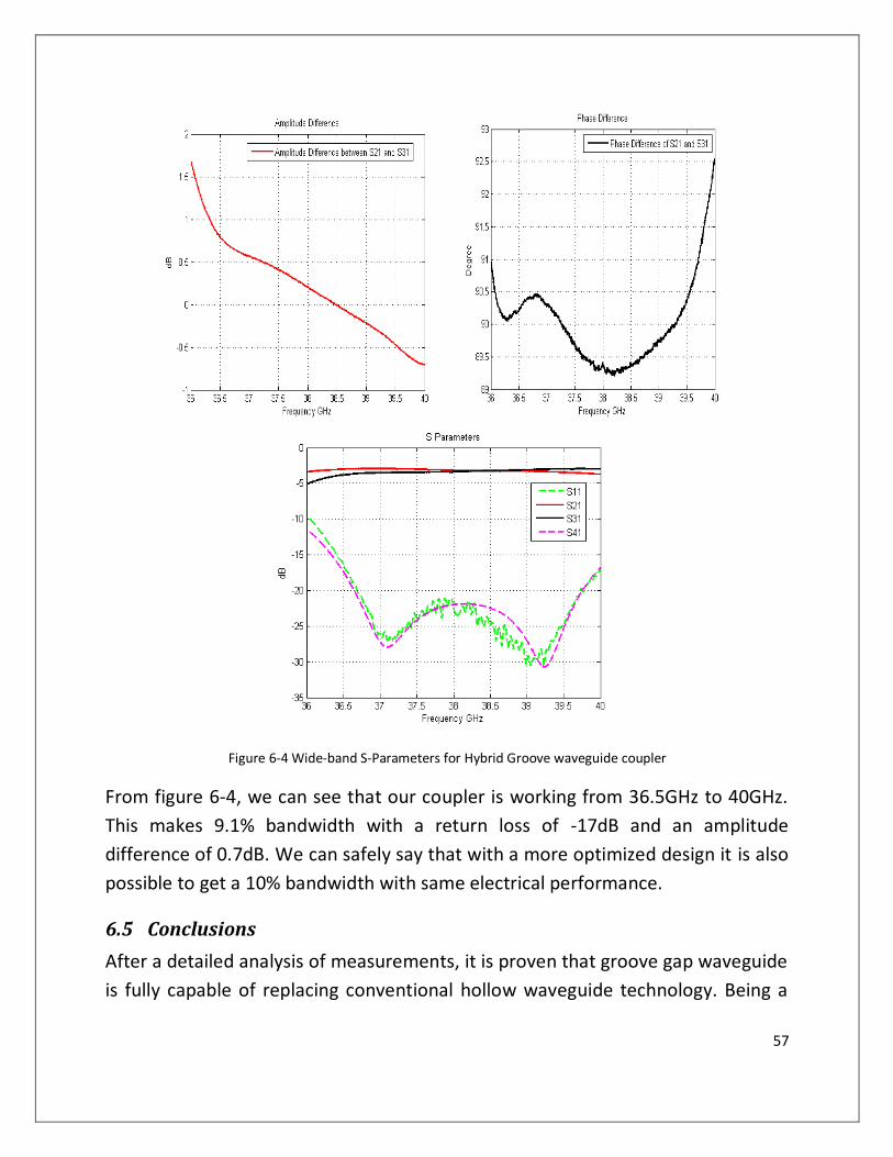
So far we have analyzed the results in our designed frequency range. But we can
observe from figure 6-1 that the coupler can work in a wider range. Therefore, in
order to estimate the total bandwidth of coupler, a plot was obtained with
extended frequency range, as shown in figure 6-4.
57
Figure 6-4 Wide-band S-Parameters for Hybrid Groove waveguide coupler
From figure 6-4, we can see that our coupler is working from 36.5GHz to 40GHz.
This makes 9.1% bandwidth with a return loss of -17dB and an amplitude
difference of 0.7dB. We can safely say that with a more optimized design it is also
possible to get a 10% bandwidth with same electrical performance.
6.5 Conclusions
After a detailed analysis of measurements, it is proven that groove gap waveguide
is fully capable of replacing conventional hollow waveguide technology. Being a

58
planar technology, it can easily be designed and optimized for different
components and frequency ranges. This report also establishes the fact that Gap
waveguides are fully compatible with conventional waveguides and same
measurement methods can be used. If we look at the design closely, we can easily
observe that it requires a large milling time and thus increases the manufacturing
costs. But on the other hand, it’s a planar technology; therefore it can be casted
using casting techniques for metal structures.
Finally we can conclude that Gap waveguide is a promising technology and a good
alternative for Terahertz applications. It has the potential to change today’s
microwave industry. Efforts are needed to integrate this technology with active
components. It requires new software techniques as well as new interface
challenges. It is anticipated that more research work will be put in this thrilling
novelistic approach and soon a terahertz device will be designed.
59
7 References
[1] A. Valero-Nogueira, E. Rajo-Iglesias, P.-S. Kildal, E. Alfonso, “Local metamaterial-based waveguides in gaps between parallel Metal Plates”, IEEE Antennas and Wire-less Propagation letters (AWPL), Vol. 19, pp. 84-7, 2009
[2] J. R. Costa, M. G. Silveirinha, C. A. Fernandes, “Electromagnetic characterization of textured surfaces formed by metallic pins”, IEEE Trans. Antennas Propag., Vol. 56, pp. 405-15, 2008.
[3] P.-S. Kildal and A. Kishk, “EM modelling of surfaces with stop or go characteristics-
artificial magnetic conductors and soft and hard surfaces”. App. Comput. Electro-magn. Soc. J., Vol.18, pp.32-34, March 2003.
[4] P.-S. Kildal, “Three metamaterial-based gap waveguides between parallel metal plates
for mm and submm waves”, in 2 9 3rd European Conference on Antennas and Propagation. EuCAP 2009, 23-27 March 2009, Piscataway, NJ, USA, 2009, pp. 28-32
[5] Per-Simon Kildal, “Foundation of antennas, a unified approach Compandium in Antenna
Engineering”, Chalmers University of Technology Sweden ,2009.
[6] Jens Bornemann Jarosla Uher, “Waveguide components for antenna feed systems” Theory and Cad, Addison Wesley, 1976.
[7] P.-S Kildal, “Definition of artificially soft and hard surfaces for electromagnetic waves”
Electron. Lett.,Vol.24, pp.168-170, 1998.
[8] Romulo F, Jimenez Broas Nicholas G, Alexopolous Dan Sievenpiper, Lijun Zhang and Eli Yablonovitch, “High-impedance electromagnetic surfaces with a forbidden frequency band”, IEEE transcations on Microwave Theory and Techniques, Vol. 47, pp.1-2, 1999.
[9] P.-S. Kildal, Eva, Rajo-Iglesias, “Cut-off bandwidth of metamaterial-based parallel-plate
gap waveguide with one textured metal pin surface”, 3rd European Conf, Antennas Propagat. (EuCAP 2009), Berlin, Germany, Vol.:23-27, March 2009.
[10] E. Rajo-Iglesias, M. Caiazzo, L.Inclan, P.S Kildal, “Comparison of bandgaps of mashroom-
type EBG surface, corrugated and strip-type soft surfaces”, IET Microw,Antenna Propag, Vol. 1, pp.1-2, Feb 2007.
[11] E. Rajo-Iglesias, Ashraf Uz Zaman, P.S Kildal, “Parallel plate cavity mode suppression in
microstrip circuit packages using a lid of nails”, IEEE Microwave and Wireless Components Letters, Vol. 20, pp.1-2, Jan 2010.

60
[12] Z.Sipus, H.Merkel, P.S Kildal, “Green's function for planar soft and hard surfaces derived
by asymptotic boundary conditions”. IEEE Proc. Part H, Vol. 47, pp.1-2, Oct. 1997.
[13] Rajo-Iglesias, P.- Kildal,”Groove gap waveguide: A rectangular waveguide between contactless metal plates enabled by parallel-plate cut-off” in 4th European Conference on Antennas and Propagation (EucCAP 2010), 12-16 April 2010, Piscataway, NJ, USA, 2010,
[14] H.J. iblet,” A mathematical theory of Directional Coupler”, I.R.E Proc, Vol.33, pp.1307-
1313), 1947
[15] H.J. iblet, “Short-Slot Hybrid Junction”, I.R.E Proc,Vol.34, pp.1307-1313, 1947
[16] Zhewang Ma, Taku Yamane, Eikichi Yamashita, “Analysis and design of H-Plane waveguide bends with compact size, wideband and low return loss characteristics”. University of Electro-Communication, Chofu-Shi Tokyo, Japan.
[17] David M.Pozar. Microwave Engineering 3rd edition. Wiley
[18] Robert E. Collins.Foundation of Microwave Engineering 3rd edition. Wiley
[19] http://www.wikipedia.com
61
8 Appendix s11=zeros(961,1); s21=zeros(961,1); s31=zeros(961,1); s41=zeros(961,1); freq=zeros(961,1); for i=1:961 freq(i,1)=S21(i,1)*10^-9; s11(i,1)=S21(i,2)+1i*(S21(i,3));
s21(i,1)=S21(i,4)+1i*S21(i,5);
s31(i,1)=S31(i,4)+1i*S31(i,5);
s41(i,1)=S41(i,4)+1i*S41(i,5);
end mag_s11=zeros(961,1); mag_s21=zeros(961,1); mag_s31=zeros(961,1); mag_s41=zeros(961,1); ang_s21=zeros(961,1); ang_s31=zeros(961,1); for i=1:961 mag_s11(i,1)=abs(s11(i,1)); mag_s21(i,1)=abs(s21(i,1)); mag_s31(i,1)=abs(s31(i,1)); mag_s41(i,1)=abs(s41(i,1)); ang_s21(i,1)=angle(s21(i,1)); ang_s31(i,1)=angle(s31(i,1)); end % for i=1:961 % mag_s11(i,1)=abs(s11(i,1)); % mag_s21(i,1)=abs(s21(i,1)); % mag_s31(i,1)=abs(s31(i,1)); % mag_s41(i,1)=abs(s41(i,1)); % end
sim_s11=zeros(961,1); sim_s21=zeros(961,1); sim_s31=zeros(961,1); sim_s41=zeros(961,1); sim_freq=zeros(961,1); for i=1:961 sim_freq(i,1)=(sim_s(i,1))*exp(9); sim_s11(i,1)=sim_s(i,4)+1i*(sim_s(i,3)); sim_s21(i,1)=sim_s(i,7)+1i*(sim_s(i,6)); sim_s31(i,1)=sim_s(i,10)+1i*(sim_s(i,9)); sim_s41(i,1)=sim_s(i,13)+1i*(sim_s(i,12));
end
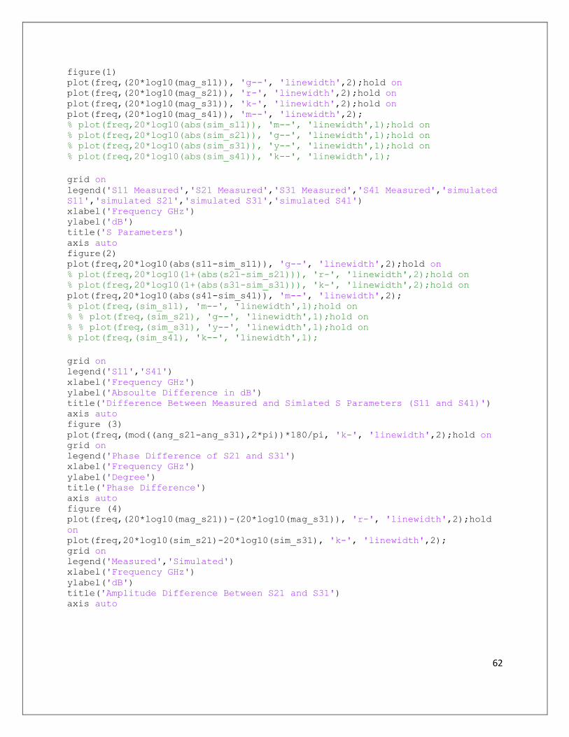
62
figure(1) plot(freq,(20*log10(mag_s11)), 'g--', 'linewidth',2);hold on plot(freq,(20*log10(mag_s21)), 'r-', 'linewidth',2);hold on plot(freq,(20*log10(mag_s31)), 'k-', 'linewidth',2);hold on plot(freq,(20*log10(mag_s41)), 'm--', 'linewidth',2); % plot(freq,20*log10(abs(sim_s11)), 'm--', 'linewidth',1);hold on % plot(freq,20*log10(abs(sim_s21)), 'g--', 'linewidth',1);hold on % plot(freq,20*log10(abs(sim_s31)), 'y--', 'linewidth',1);hold on % plot(freq,20*log10(abs(sim_s41)), 'k--', 'linewidth',1);
grid on legend('S11 Measured','S21 Measured','S31 Measured','S41 Measured','simulated
S11','simulated S21','simulated S31','simulated S41') xlabel('Frequency GHz') ylabel('dB') title('S Parameters') axis auto figure(2) plot(freq,20*log10(abs(s11-sim_s11)), 'g--', 'linewidth',2);hold on % plot(freq,20*log10(1+(abs(s21-sim_s21))), 'r-', 'linewidth',2);hold on % plot(freq,20*log10(1+(abs(s31-sim_s31))), 'k-', 'linewidth',2);hold on plot(freq,20*log10(abs(s41-sim_s41)), 'm--', 'linewidth',2); % plot(freq,(sim_s11), 'm--', 'linewidth',1);hold on % % plot(freq,(sim_s21), 'g--', 'linewidth',1);hold on % % plot(freq,(sim_s31), 'y--', 'linewidth',1);hold on % plot(freq,(sim_s41), 'k--', 'linewidth',1);
grid on legend('S11','S41') xlabel('Frequency GHz') ylabel('Absoulte Difference in dB') title('Difference Between Measured and Simlated S Parameters (S11 and S41)') axis auto figure (3) plot(freq,(mod((ang_s21-ang_s31),2*pi))*180/pi, 'k-', 'linewidth',2);hold on grid on legend('Phase Difference of S21 and S31') xlabel('Frequency GHz') ylabel('Degree') title('Phase Difference') axis auto figure (4) plot(freq,(20*log10(mag_s21))-(20*log10(mag_s31)), 'r-', 'linewidth',2);hold
on plot(freq,20*log10(sim_s21)-20*log10(sim_s31), 'k-', 'linewidth',2); grid on legend('Measured','Simulated') xlabel('Frequency GHz') ylabel('dB') title('Amplitude Difference Between S21 and S31') axis auto
![Improving the detection limit for on chip photonic sensors ...These include ring slot resonators [14, 15], slot waveguides [16], nano-holes [17], low index modes [8], slow light effect](https://img.pdfslide.us/doc/110x75/5ff1dd1ee9b110486d79561e/improving-the-detection-limit-for-on-chip-photonic-sensors-these-include-ring.jpg)


![Analysis of S-X Band Slot Coupled Wave Guide Junction · 900 and coupling is through inclined slot in the narrow wall of rectangular waveguides. Hsu et al. [11] obtained some admittance](https://img.pdfslide.us/doc/110x75/5ebe4e226dff7c0e0f2bada3/analysis-of-s-x-band-slot-coupled-wave-guide-junction-900-and-coupling-is-through.jpg)


![PROCEEDINGS OF SPIE · 9450 0V Bi-directional triplexer with butterfly MMI coupler using SU-8 polymer waveguides [9450-104] 9450 0W Micro-optical insertion system for WDM transceiver](https://img.pdfslide.us/doc/110x75/5f4b1c532266e369e97e6ef6/proceedings-of-spie-9450-0v-bi-directional-triplexer-with-butterfly-mmi-coupler.jpg)