Embed Size (px)
Citation preview
SSHHAAPPEE MMEEMMOORRYY AALLLLOOYY LLAATTCCHHIINNGG MMIICCRROOAACCTTUUAATTOORR
By Stacy Cabrera, Nicole Harrison, David Lunking, Rebecca Tang, Theresa Valentine,
and Christopher Ziegler
ENMA 490 Fall 2002 Professor Gary Rubloff
The goal of this project was to design a MEMS device that uses cutting edge materials. After researching different MEMS devices and smart materials, the group decided on a shape memory alloy microactuator. Shape memory alloys make use of a twinning property that allows them to change shape upon heating. The material changes from a mechanically formed shape in its cold martensite state to a “remembered” shape in its heated austenite state. When it cools, the material once again can be mechanically deformed. A literature search only turned up one result that detailed a valve using SMA arms to lift a Si island. The group decided to improve upon this design by changing the mechanical structure and turning the actuator into a latching device that reduces power usage. The design process evolved from a mechanical latch and two-way SMAs to one-way SMAs deposited on cantilevers with a magnetic latch. Calculations were done to figure out the possible cantilever deflection, which ranged from 1 micron to 0.1 millimeter depending on the size of the cantilever and the thickness of the SMA. The process flow developed for the actuator involved the mask design and the training and annealing of the SMAs. The SMA used is NiTi and the substrate is either Si or GaAs. The device constraints are evaluated and possible applications are mentioned within the report. The primary application of the actuator is for electrical contacts and secondary ones are optical mirrors, valves, and drug delivery systems. Future research can be done regarding optimization of the device properties and a model of the device can be built.
1. INTRODUCTION Problem Statement
The goal of the project was to develop a latching shape-memory alloy (SMA) microactuator. An existing design of a SMA microvalve that served as a microactuator and had new technology that could be improved upon was found in an article, The Characterization of TiNi Shape-Memory Actuated Microvalves (Lai, 2001). A newer design was needed that incorporated SMAs and latching technology. The article State-of-the-art Shape Memory Actuators (Johnson, Kramer 1998) describes the current state of SMA actuator development and mentions a movement to a latching design and manufacturing on the micron scale as the next step in processing. The existing design consumed power the entire time the valve was kept in its secondary state (open or closed depending on design) and was on the millimeter scale. A newer design was needed that used microelectromechanical systems (MEMS), used lower power consumption, and was smaller. The primary goal of reducing power consumption can be fixed by converting the actuator to a latching design and the system can be downsized to the micrometer scale (See Figure 1a).
Background
MEMS devices are microelectromechanical systems that can be used in many applications such as sensors and actuators. In general, MEMS involve both electric and non-electric parts and perform functions that include sensing, actuating, signal processing, displaying, and controlling (Senturia, 2001). They can be used in chemical, mechanical, and medical applications. In the case of this project, the group is working on actuators--devices that trigger an action response.
MEMS are made from a variety of processes, mostly involving some form of lithography-based microfabrication combined with micromachining. For three-dimensional devices, thin-film deposition, etching, and wafer-bonding techniques are used to make the creation of moving parts possible. Silicon is commonly used in these processes because the machines are already calibrated to match the properties of silicon wafers. Inorganic materials such as silicon, silicon dioxide, silicon nitride, aluminum, and tungsten as well as some polymers are often used in MEMS (Senturia, 2001).
This project will investigate wafer-bonding, optical lithography, masking, and etching as the processes used for manufacturing the actuator.
Initial Concept
The initial response to the problem was to develop a “latching” design for the already established SMA microvalve to save power. The group wanted some way to hold the secondary state of the valve (open or closed depending on design) without applying continuous power. Several design concepts were offered including: a technical latching model using ferromagnetics (see materials section) controlled by magnetic fields, a mechanical latching model using a pushing object and Velcro (Figure 1c), and a smart materials model using a two-way SMA. The group decided that a latching design was possible. The next step was to decide how and why a latching model worked better than a conventional actuator that required continuous power. The decision to pursue a latching
1

design was chosen after comparing the duty cycles of latching and non-latching designs as seen in Figures 1a and 1b. Previous Research An article on SMA microvalve actuators was published in 2001 that discussed a valve design that was normally closed (Lai, 2001). Power had to be applied continuously to heat the TiNi SMA wires to keep the valve open. The design included 8 SMA wires connected to a Si island in a square shaped valve on the millimeter scale. Figure 1d shows the microactuator developed at Case Western University. Dr. Manfred Wuttig in the Department of Materials Engineering at the University of Maryland has also done extensive research on SMAs, thin film SMAs. Shape memory alloys, especially nickel-titanium alloys, have been of interest lately because of their use as microactuators in microelectromechanical systems (MEMS). Manfred Wuttig and his colleagues at the University of Maryland, College Park have studied TiNi thin films in order to better understand the properties of shape memory alloys as thin films. Research shows that bimorphs of one-dimensional thin film strips patterned on to two-dimensional silicon substrates under uniaxial stresses have increased transformation-induced deflection (Mori et al., 2002). The bimorph cantilever systems also have decreased thermo-elastically induced deflection compared to the bimorphs of unpatterned, planar TiNi thin films on silicon substrates (Mori et al., 2002). When double layering the patterned strips onto silicon substrates at different deposition temperatures, it has been observed that depositing strips at decreasing temperatures produces high damping while depositing TiNi strips upon heating produces larger actuation and stress relief (Wuttig, 2002). The results of the studies help to determine the type of patterning that provides better actuation as well as whether microactuators should contain multiple layers of SMA thin films in order to increase the properties of the device. A literature search was performed in late October and early November to determine if there has been any previous research or designing of a latching SMA microactuator. Articles were found that described SMA microactuators but none with a latching component. Power had to be continuously supplied in all cases. One abstract was found that described thin film SMA latching microactuators. “In this paper, the development of TiNi thin film actuated, high current carrying, latching microrelays are described” (Galhotra et al., 2000). However, the full text of this paper could not be found. Both US patents and academic articles were searched. The group proceeded with the project under the assumption that its design of a latching SMA microactuator is unprecedented.
2

Definitions Shape Memory Alloys (SMAs): metal alloys that can recover apparent permanent strain when they are heated to their phase transition temperature. These materials switch from martensite phase to austenite phase upon heating and then back to martensite upon cooling. When heated, the SMA returns to the shape it was formed in, resulting in what is termed the shape memory effect. Latching: in reference to a SMA actuator the device catches between modes so that power does not have to be continuously applied. The device will heat to the transition temperature, change to austenite and then remain in that state after the power is removed. Then the device will “unlatch” when it needs to return to its original state. Duty Cycle: the ratio of the on-time to the period of the power transfer switch when it is taking energy from the source. It is (on-time)/(on-time + off-time), a dimensionless parameter falling within the values 0 and 1. Cantilever: a beam (much longer than it is wider) that is bendable and is attached on one end and free on the other.
3

Section 1 Figures
Cummulative Energy Comparison
0
5
10
15
20
0 5 10 15 20Time
Cum
mul
ativ
e En
ergy
Non-latching Latching
Power Comparison
0
0.4
0.8
1.2
0 5 10 15 20Time
Pow
er
Latching Non-latching
Figures 1a and 1b show power usage and cumulative energy comparisons between latching and non-latching actuators for several switching cycles.
Velcro loops
Velcro hooks
Velcro hooks
Another TWSMAunder “loops”
Actuates with more force than Velcro has, releases cantilever
Velcro loops
Velcro hooks
Returns to cold shape, ready for another cycle
Figure 1c shows one of the early designs using mechanical latching--Velcro that holds a two-way SMA.
Figure 1d is the valve from the Case Western University group that uses SMA arms to lift a Si island to open the valve.
4
2. PROJECT EVOLUTION The first step in the design process was finding something to design. Our initial constraints were that the device had to be MEMS, and that it should use a new material in a novel way. After brainstorming individually, we each came up with design proposals ranging from a telescope mirror arrays to implanted medical devices. For each proposal, we tried to look at what materials were to be used, what would the device do, and what its applications could be. This concept of a design triangle became the backbone of our project. After rethinking our ideas in terms of this triangle, we came to the conclusion that all of the ideas were too complex and we would not be able to decide on just one of them. We had to come up with something simple that all of our proposed devices could use. Going back to our new materials constraint, we thought about new materials and came upon shape memory alloys. This led to the idea for an actuating device. Some sort of actuator was a major component in all of our designs. But our device would have to be a new idea, and SMA actuators already exist at almost a MEMS scale. One thing that none of us had seen was a latching SMA actuator. Since MEMS latching SMA actuators could be used in all of our ideas, we already had a number of applications for it. Finally we had completed the basic design triangle. There were two different types of SMA considered, thermally actuated and magnetically actuated. The thermally actuated TiNi had already been used and tested giving us a basis to work on. Not enough is known about magnetic SMA properties, and it would have been too hard to control the magnetic field in the simple kind of device we wanted. Since we knew more about it, we agreed on using TiNi as our SMA material. The next step was determining out how to latch the actuator. The initial idea was a swinging door-like device that gets caught on “micro-Velcro”, a physical barrier, or a magnet (Figure 1c). Soon after this, the design became two blocks each suspended from NiTi wires over the contact area (Figure 2a). A magnet would be used to seal the contact. There were several different versions of each design to compensate for processing restrictions (Figure 2b). After weeks of trying to find a way to actually build one of these designs, another design that might be easier to make was introduced. It used two cantilevers coated with NiTi (Figure 2c) and a magnet to hold the latch. This became our final design. Although it is easier to fabricate, there are still barriers such as attaching the two cantilevers together and figuring out the specifics of the magnet. In terms of organization, we had to split up group members’ work and prioritize. We chose what each person in the group would work on according to interest and expertise. We had to make some aspects of the design secondary to others. Neither the glue needed for attaching the cantilevers together nor the magnet were specified, assuming instead they could be found later under less of a time constraint.
5

Section 2 Figures
Figure 2a is the initial "block and spring" design going from the closed position to the open position
and then back to closed.
Figure 2b shows different versions for an actuator to deal with production difficulties.
Contact
Direction of Flow Direction of Latch Movement
Substrate
a.) b.) c.)
Fig 2.2 First design’s different processing schemes versus flow in device
6
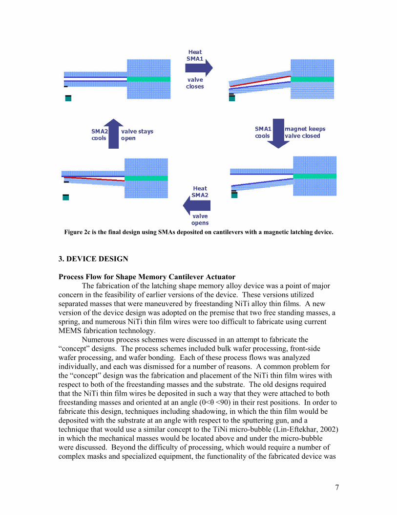
Figure 2c is the final design using SMAs deposited on cantilevers with a magnetic latching device.
3. DEVICE DESIGN Process Flow for Shape Memory Cantilever Actuator
The fabrication of the latching shape memory alloy device was a point of major concern in the feasibility of earlier versions of the device. These versions utilized separated masses that were maneuvered by freestanding NiTi alloy thin films. A new version of the device design was adopted on the premise that two free standing masses, a spring, and numerous NiTi thin film wires were too difficult to fabricate using current MEMS fabrication technology.
Numerous process schemes were discussed in an attempt to fabricate the “concept” designs. The process schemes included bulk wafer processing, front-side wafer processing, and wafer bonding. Each of these process flows was analyzed individually, and each was dismissed for a number of reasons. A common problem for the “concept” design was the fabrication and placement of the NiTi thin film wires with respect to both of the freestanding masses and the substrate. The old designs required that the NiTi thin film wires be deposited in such a way that they were attached to both freestanding masses and oriented at an angle (0<θ <90) in their rest positions. In order to fabricate this design, techniques including shadowing, in which the thin film would be deposited with the substrate at an angle with respect to the sputtering gun, and a technique that would use a similar concept to the TiNi micro-bubble (Lin-Eftekhar, 2002) in which the mechanical masses would be located above and under the micro-bubble were discussed. Beyond the difficulty of processing, which would require a number of complex masks and specialized equipment, the functionality of the fabricated device was
7

questioned in terms of whether or not the key component, the SMA thin film, would laminate upon cycling.
A problem for the front-side processing (micro-device fabrication using only one surface of the substrate) and bulk processing methods was the formation of two separated mechanical masses. In order to obtain the two separated masses using just one substrate required numerous steps as well as separation techniques that could not take advantage of photolithography due to each mass blocking the light’s path to the other. This problem led to a seemingly feasible “horizontal” design in which the mechanical masses moved in a plane parallel to the substrate material. Upon further consideration, this feasible horizontal design suffered from the same film deposition and placement issues as the vertical design, yet allowed for relatively easy freestanding mass formation.
Wafer bonding was also discussed to create the freestanding masses. This method, which would have used two separately patterned substrates and a specialized substrate bonding technique, was quickly dismissed due to the high temperature requirement for wafer bonding. With thin film already deposited on each individual wafer, high temperature bonding probably would have caused the TiNi thin film to degrade and lose functionality.
Keeping the requirement of freestanding masses controlled by shape memory thin film, the initial concept design was discarded in favor of a revolutionary cantilever design. This design incorporated the use of two bulk-processed cantilevers with thin films separately deposited on each. The design eliminates the need for additional process steps to include a spring, because the cantilever substrate material has an inherent spring constant (Young’s modulus). It allows for the non-complicated processing of numerous devices on each wafer, and significantly decreases the energy required for processing, when compared to the high-temperature deposition steps discussed in previous design process flows.
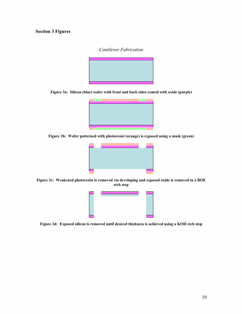
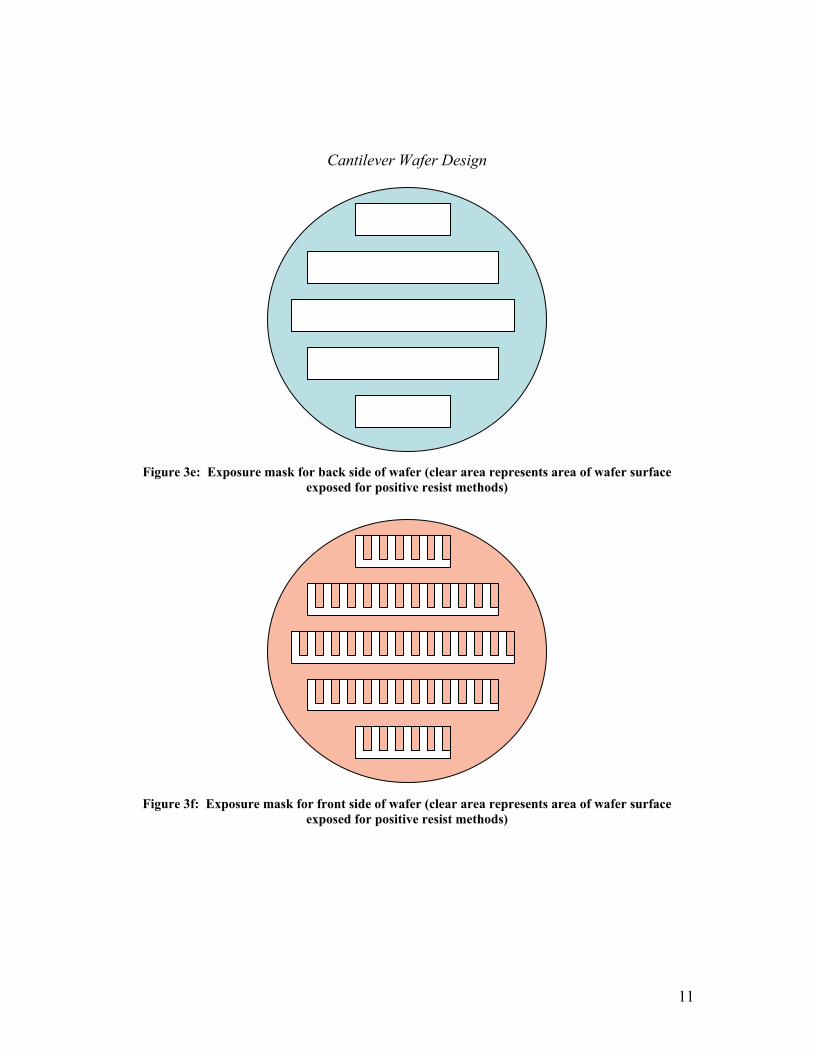
To fabricate each individual cantilever, a silicon substrate with a thin layer of oxide on both front- and backsides (Figure 3a) is processed using photolithography. The photolithography step requires each mask (Figure 3e and 3f) to be aligned exactly with one another (Figure 3b). After both back and front sides are patterned, exposed, and developed, exposed oxide is removed using HF solution (Figure 3c) leaving exposed silicon. The exposed silicon is then etched away using potassium hydroxide until the desired cantilever thickness is obtained (Figure 3d). The processed cantilever wafer can then have NiTi thin film deposited on its front-side by sputtering and can then be annealed at a temperature around 500oC. This process flow was adopted from University of Maryland materials professor Ichiro Takeuchi’s combinatorial experiments. Two cantilevers make up one device and are oriented parallel to each other in the final packaging process. Packaging
Device packaging is vital to the success of the final product, but has very little to do with the basic functionality of the SMA latching actuator. The packaging of the device requires that each cantilever be separately “glued” to the packaging material and spaced accordingly based on application parameters. A demand on the packaging not driven by application parameters is the placement of a magnet to hold the bottom cantilever down when actuation occurs. It is critical that the packaging comply with our
8

goal of creating a SMA latching actuator. This eliminates most mechanical means of holding the cantilever down (gears, wheels, and moving parts) as well as high power electromagnets, piezoelectrics, and other shape memory alloy cantilevers to name a few. A permanent magnet, chosen based on necessary cantilever deflection and accompanying forces for specific applications should provide enough attractive force to the magnetic material deposited on the cantilever to hold the cantilever down without expending continuous energy. Upon reheating of the cantilever and NiTi thin film, the magnetic force between the two magnets should be considered negligible compared to the force generated by the contraction of the thin film in the device’s progress to its relaxed state. Process Flow and Device Functionality
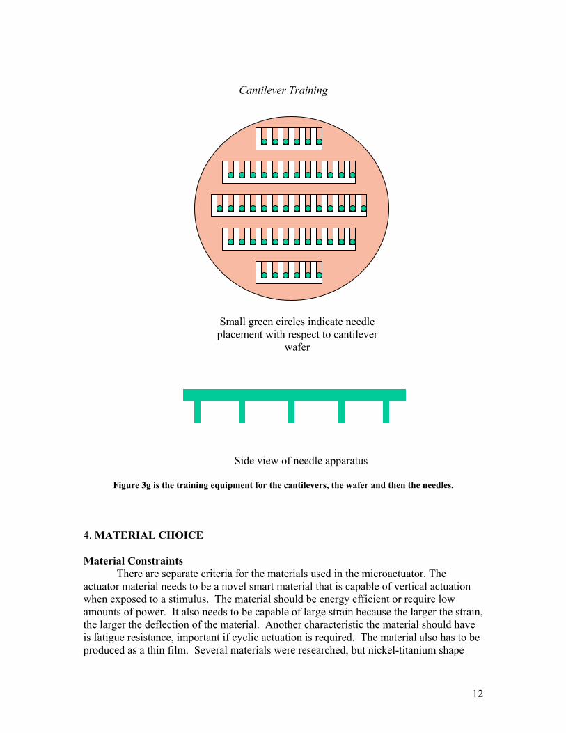
The shape memory alloy thin film must be trained during the annealing process in the high temperature parent phase (austenite) in order for the film to remember its shape and allow for SMA driven actuation. A simple structure that utilizes stiff needles (Figure 3g) would be used to push down the cantilevers to the application-specific degree of actuation during annealing. The stress induced by the stiff needles will trigger the martensite phase and allow the domains to orient themselves parallel with the applied stress. Maintaining this stress for a given amount of time will result in the thin film “remembering” its martensite orientation.
9
Section 3 Figures
Cantilever Fabrication
Figure 3a: Silicon (blue) wafer with front and back sides coated with oxide (purple)
Figure 3b: Wafer patterned with photoresist (orange) is exposed using a mask (green)
Figure 3c: Weakened photoresist is removed via developing and exposed oxide is removed in a BOE etch step
Figure 3d: Exposed silicon is removed until desired thickness is achieved using a KOH etch step
10
Cantilever Wafer Design
Figure 3e: Exposure mask for back side of wafer (clear area represents area of wafer surface exposed for positive resist methods)
Figure 3f: Exposure mask for front side of wafer (clear area represents area of wafer surface exposed for positive resist methods)
11
Cantilever Training
Small green circles indicate needle placement with respect to cantilever
wafer
Side view of needle apparatus
Figure 3g is the training equipment for the cantilevers, the wafer and then the needles. 4. MATERIAL CHOICE Material Constraints
There are separate criteria for the materials used in the microactuator. The actuator material needs to be a novel smart material that is capable of vertical actuation when exposed to a stimulus. The material should be energy efficient or require low amounts of power. It also needs to be capable of large strain because the larger the strain, the larger the deflection of the material. Another characteristic the material should have is fatigue resistance, important if cyclic actuation is required. The material also has to be produced as a thin film. Several materials were researched, but nickel-titanium shape
12
memory alloys were the best choice for this design. The substrate material should provide support for the SMA and be deformable when a stress is applied. Possible substrate materials are copper, silicon, and galium arsenide. Both materials have to be able to be fabricated using MEMS processing techniques. Shape Memory Alloys
Shape memory alloys (SMAs) have been of interest since their discovery in the 1930's by Olander, but more recently because of their potential applications in microelectromechanical systems (Gill et al., 2001). Shape memory alloys have desirable properties like high work output per unit volume, super-elasticity, and high damping capacity that make them suitable for use in actuators. The fact that they can be actuated by joule heating with an electric current or with heat transfer is also a plus. However, it is their shape memory effect that makes them unique compared to other actuator materials.
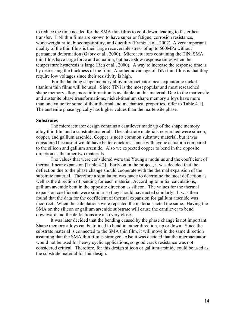
The shape memory effect is the thermally induced transformation between a martensite phase at low temperatures and an austenite phase at high temperatures (Gu et al., 1998). Figure 1 shows how SMAs start off in their parent phase, the ordered austenite phase and when the material is cooled below the martensitic temperature, the structure of the SMA becomes twinned. When in the martensite phase the material can be easily deformed into other shapes with relatively little force. Applying a stress to the shape memory alloy reorganizes the twin orientations along the direction of the stress (Surbled et al, 2001). Upon heating above the austenite temperature, the crystal structure converts back to its highly ordered parent phase and the original SMA structure is recovered.
In order to use shape memory alloys for specific applications the materials have to be set or trained to a specific shape. The SMAs are constrained to mandrels or fixtures with the desired shape and are then heat treated for specific amounts of time. The time and temperature needed to train the SMA depends on the type of SMA used. The heat treatment is applied so that at that temperature the material remembers to go to that particular shape. When heat treating, care must be taken to make sure the SMA reaches the required temperature and is held at that temperature for enough time. If heat treatments are to high then there can be an increase in the actuation temperature and the material can have a sharper thermal response.
When comparing bulk SMAs to SMA thin films, SMA thin films are preferred because of their large energy density, high frequency response, and long lifetime at smaller dimensions. SMA thin films can be fabricated in batch, patterned with standard lithographic techniques, and engineered into micron-size structures (Fu & Du, in press). According to Ren, Wang, Xu, and Cai (2000), the properties of SMA thin films strongly depend on the metallurgical factors as well as deposition conditions used to fabricate them. For nickel titanium thin films, their properties have been assumed to be the same as bulk nickel-titanium.
Nickel-Titanium
Nickel titanium is considered to be the best type of shape memory alloy compared to other popular polycrystalline SMAs like CuZnAl and CuAlNi (Huang, 2002). TiNi thin films have small thermal masses and large surface to volume ratios that enable them
13
to reduce the time needed for the SMA thin films to cool down, leading to faster heat transfer. TiNi thin films are known to have superior fatigue, corrosion resistance, work/weight ratio, biocompatibility, and ductility (Frantz et al., 2002). A very important quality of the thin films is their large recoverable stress of up to 500MPa without permanent deformation (Gabry et al., 2000). Microactuators containing the TiNi SMA thin films have large force and actuation, but have slow response times when the temperature hysteresis is large (Ren et al., 2000). A way to increase the response time is by decreasing the thickness of the film. Another advantage of TiNi thin films is that they require low voltages since their resistivity is high.
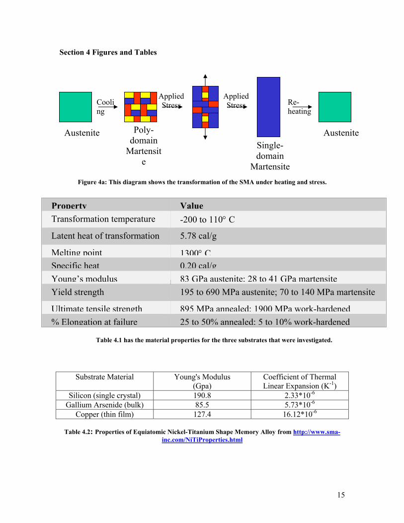
For the latching shape memory alloy microactuator, near-equiatomic nickel-titanium thin films will be used. Since TiNi is the most popular and most researched shape memory alloy, more information is available on this material. Due to the martensite and austenite phase transformations, nickel-titanium shape memory alloys have more than one value for some of their thermal and mechanical properties [refer to Table 4.1]. The austenite phase typically has higher values than the martensite phase. Substrates The microactuator design contains a cantilever made up of the shape memory alloy thin film and a substrate material. The substrate materials researched were silicon, copper, and gallium arsenide. Copper is not a common substrate material, but it was considered because it would have better crack resistance with cyclic actuation compared to the silicon and gallium arsenide. Also we expected copper to bend in the opposite direction as the other two materials.
The values that were considered were the Young's modulus and the coefficient of thermal linear expansion [Table 4.2]. Early on in the project, it was decided that the deflection due to the phase change should cooperate with the thermal expansion of the substrate material. Therefore a simulation was made to determine the most deflection as well as the direction of bending for each material. According to initial calculations, gallium arsenide bent in the opposite direction as silicon. The values for the thermal expansion coefficients were similar so they should have acted similarly. It was then found that the data for the coefficient of thermal expansion for gallium arsenide was incorrect. When the calculations were repeated the materials acted the same. Having the SMA on the silicon or gallium arsenide substrate will cause the cantilever to bend downward and the deflections are also very close.
It was later decided that the bending caused by the phase change is not important. Shape memory alloys can be trained to bend in either direction, up or down. Since the substrate material is connected to the SMA thin film, it will move in the same direction assuming that the SMA thin film is stronger. Also it was decided that the microactuator would not be used for heavy cyclic applications, so good crack resistance was not considered critical. Therefore, for this design silicon or gallium arsinide could be used as the substrate material for this design.
14
Section 4 Figures and Tables
Applied Stress
Austenite
Re- heating
Applied Stress
Poly-domain
Martensite
Cooling
Austenite Single-domain
Martensite
Figure 4a: This diagram shows the transformation of the SMA under heating and stress.
Table 4.2: This table shows properties of the materials looked at for substrate choices.
25 to 50% annealed; 5 to 10% work-hardened% Elongation at failure895 MPa annealed; 1900 MPa work-hardenedUltimate tensile strength
195 to 690 MPa austenite; 70 to 140 MPa martensiteYield strength 83 GPa austenite; 28 to 41 GPa martensiteYoung’s modulus0.20 cal/gSpecific heat1300° CMelting point
5.78 cal/g Latent heat of transformation
-200 to 110° C Transformation temperature ValueProperty
Table 4.1 has the material properties for the three substrates that were investigated.
Substrate Material Young's Modulus (Gpa)
Coefficient of Thermal Linear Expansion (K-1)
Silicon (single crystal) 190.8 2.33*10-6 Gallium Arsenide (bulk) 85.5 5.73*10-6
Copper (thin film) 127.4 16.12*10-6
Table 4.2: Properties of Equiatomic Nickel-Titanium Shape Memory Alloy from http://www.sma-inc.com/NiTiProperties.html
15
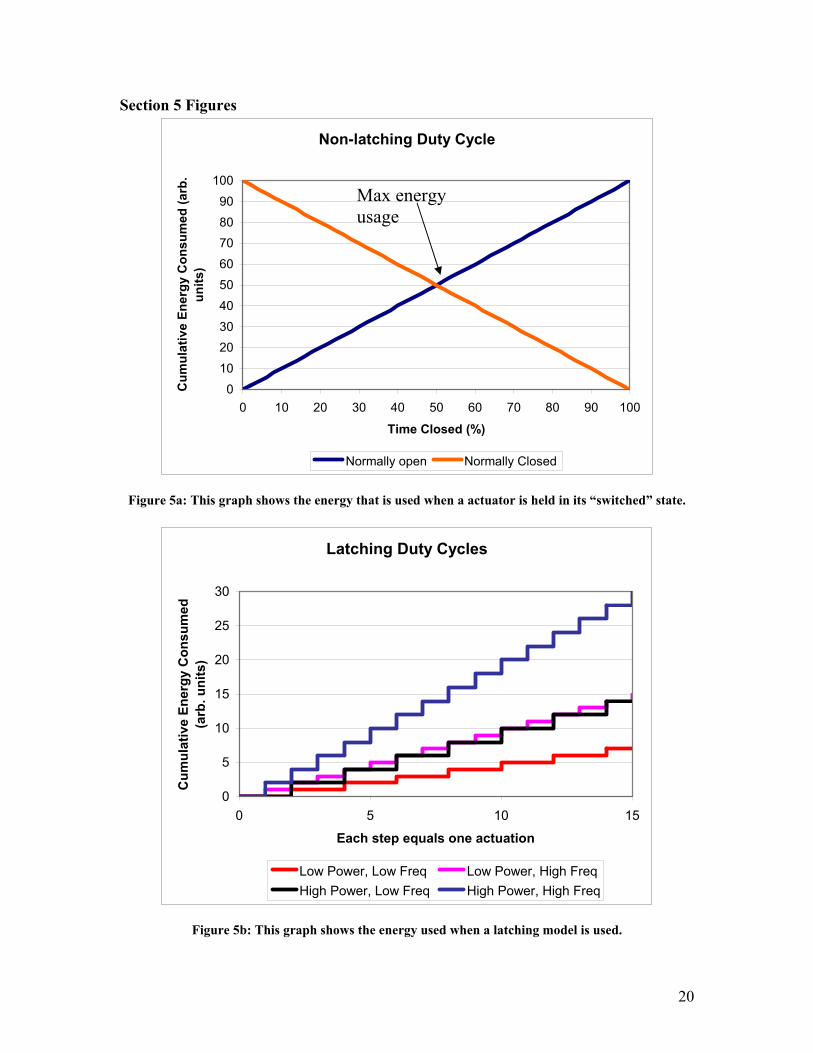
5. DESIGN EVALUATION Power Calculations and Tradeoff Duty Cycles
Non-Latching: Traditional non-latching actuator designs require the constant input of energy to remain in their secondary state. As a result, the amount of energy expended is a function of the time the actuator remains in the secondary state and the power needed to maintain the switched state. This translates to a linear energy consumed = power * time (See Figure 5a).
There are two types of non-latching actuators: normally open and normally closed. When power is shut off, each of these types will revert to its base state, (e.g., open for a normally open actuator). If the actuator application requires it to spend only a small percentage of its time in the secondary state, then the amount of energy expended will be very small. If the application requires that the majority of the time be spent in the secondary state, then using the other actuator type (such as normally closed instead of normally open) will result in lower power consumption. When 50% of the time is spent in the secondary state, then either type of actuator will consume the same amount of energy. This results in one actuator choice being better for large secondary state times, while both are equally suited for near half and half times.
Latching: The latching actuator however, requires energy only to shift states, e.g. from open to closed. Therefore, the energy used is merely a multiple of the number of times the actuator shifts state, i.e. opens or closes. Power is consumed at a rate that is independent of the total amount of time the actuator is in its secondary state. Instead, the cumulative energy consumed = energy per cycle * frequency of operation * amount of time used.
As a result, there are several different possible energy configurations for a latching actuator. These are the combinations of low power, high power, low frequency, and high frequency. From these possibilities there are four different duty cycles that become apparent (See Figure 5b). Power is dependent on the actual device itself and how much energy is needed to actuate the device. Frequency is an application parameter that depends on how the device is used.
As can be seen in Figure 5b, low power and low frequency offers the best options for energy savings. However, high power is merely a scalar multiple of low power, and is determined by the properties of the device.
The significant difference appears with high frequency applications. Rapidly switching the state of the latching actuator requires significantly more energy per time than low frequency shifting. This means that at some critical operational frequency, a non-latching actuator will in fact use the same amount of energy as the latching actuator. At any higher frequency, the non-latching actuator is in fact more energy efficient.
This cycle dependent energy efficiency yields interesting application possibilities. First, for applications where the state needs to be changed at a low frequency and held for a long time, the latching actuator is more energy efficient. Secondly, if the needs of the application are uncertain or varying but are require the actuator to be in the secondary
16

state approximately 50% of the, then the latching actuator can potentially offer significant energy savings for low frequency applications. Power for Heating SMAs To determine the power consumed by our latching microactuator, we created a simple simulation with VisSim 4.5 (Visual Solutions, Inc.). By equating the power equations for current flow (Equation 5.1) and thermal conductivity (Equation 5.2), the current necessary to heat the actuating cantilever to the austenite-finish temperature (Af) could be determined. Because of different thermal conductivity and resistivity of the martensite and austenite phases of the SMA film, the current required to heat the cantilever changes during the transformation. Taking the maximum current value (either austenite or martensite) and assuming that a power source would be programmed to deliver this current constantly, the power required throughout the SMA-heating process could be calculated from Equation 5.1. Figure 5c shows this relationship for a response time of 0.01 seconds and an Af of 140ºC; the power is turned off once the cantilever reaches this temperature. A total of 0.97mJ of energy is necessary per heating cycle for the chosen configuration; therefore, 0.97mJ is needed to change the state of the actuator (assuming both cantilevers are the same).
substrateSMA RR
IRIP11
122
+== (5.1)
responset
TmCP ∆= (5.2)
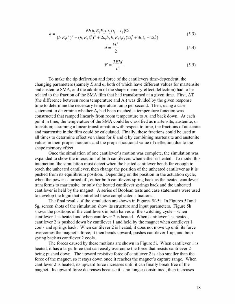
m - mass of cantilever, c - specific heat of cantilever, ∆T - difference between Af and room temperature, t - desired response time, I – current applied, R – resistance of the cantilever Cantilever Deflections and Forces Modeling the positions of the cantilevers with respect to time throughout the switching cycle of the actuator was extremely complicated. The basis for the entire simulation was the idea that non-uniform shape changes in the SMA film and substrate cause curvature in the cantilever (see Figure 5d for a graphical “rationale” of this idea). The non-uniform shape change could be produced either by thermal expansion on heating or by lattice-parameter change during the martensite-to-austenite transformation. For the case of thermal expansion, equations for tip deflection of a bimetallic cantilever had already been derived in the literature (Chu, 1993). Using beam theory, Equation 5.3 could be derived for the curvature of the beam*. Equations 5.4 and 5.5 relate the curvature to tip deflection and tip deflection to tip force, respectively.
* For this equation, Figure 5f shows the notation for the cantilever dimensions, E represents the Young’s modulus of the material, and Ω represents a strain term that equals ∆T(α2 – α1) for thermal expansion and |1 - (aaust/amart)| for shape memory effect. The parameters aaust and amart are the lattice constants of the austenite and martensite phases, selected in such a manner that the shape change is consistent with the shape change from thermal expansion (i.e., if thermal expansion makes the SMA film expand more than the substrate, we want the austenite SMA to get even bigger than the martensite to enhance the bending). These lattice constants were found in the literature (Huang, 1999).
17
)232(2)()()(6
2221
21212121
22222
22111
21212121
ttttttEEbbtEbtEbttttEEbbk
++++Ω+
= (5.3)
2
2kLd = (5.4)
3
3LEIdF = (5.5)
To make the tip deflection and force of the cantilevers time-dependent, the changing parameters (namely E and α, both of which have different values for martensite and austenite SMA, and the addition of the shape-memory-effect deflection) had to be related to the fraction of the SMA film that had transformed at a given time. First, ∆T (the difference between room temperature and Af) was divided by the given response time to determine the necessary temperature ramp per second. Then, using a case statement to determine whether Af had been reached, a temperature function was constructed that ramped linearly from room temperature to Af and back down. At each point in time, the temperature of the SMA could be classified as martensite, austenite, or transition; assuming a linear transformation with respect to time, the fractions of austenite and martensite in the film could be calculated. Finally, these fractions could be used at all times to determine effective values for E and α by combining martensite and austenite values in their proper fractions and the proper fractional value of deflection due to the shape memory effect. Once the simulation of one cantilever’s motion was complete, the simulation was expanded to show the interaction of both cantilevers when either is heated. To model this interaction, the simulation must detect when the heated cantilever bends far enough to reach the unheated cantilever, then change the position of the unheated cantilever as it is pushed from its equilibrium position. Depending on the position in the actuation cycle, when the power is turned off, either both cantilevers spring back as the heated cantilever transforms to martensite, or only the heated cantilever springs back and the unheated cantilever is held by the magnet. A series of Boolean tests and case statements were used to develop the logic that controlled these complicated situations. The final results of the simulation are shown in Figures 5f-5i. In Figures 5f and 5g, screen shots of the simulation show its structure and input parameters. Figure 5h shows the positions of the cantilevers in both halves of the switching cycle – when cantilever 1 is heated and when cantilever 2 is heated. When cantilever 1 is heated, cantilever 2 is pushed down by cantilever 1 and held by the magnet when cantilever 1 cools and springs back. When cantilever 2 is heated, it does not move up until its force overcomes the magnet’s force; it then bends upward, pushes cantilever 1 up, and both spring back as cantilever 2 cools.
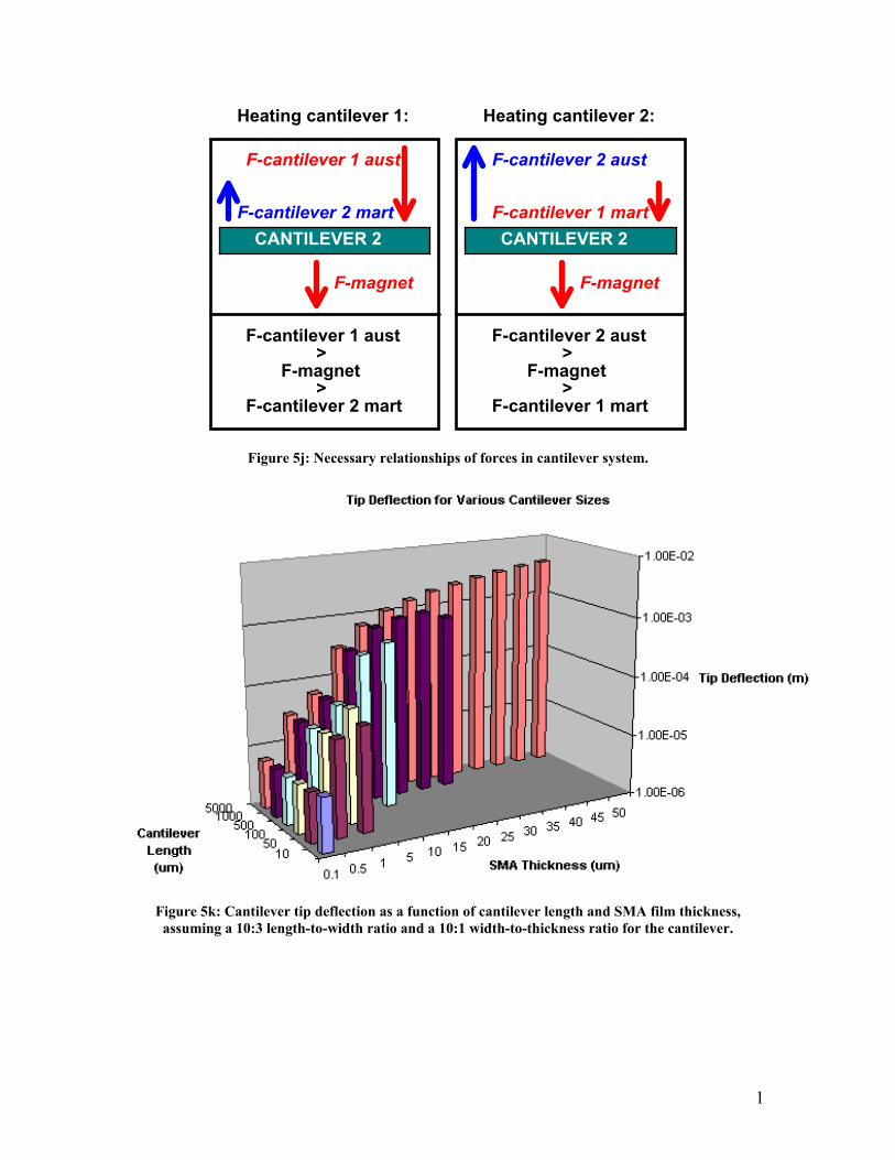
The forces caused by these motions are shown in Figure 5i. When cantilever 1 is heated, it has a large force that can easily overcome the force that resists cantilever 2 being pushed down. The upward resistive force of cantilever 2 is also smaller than the force of the magnet, so it stays down once it reaches the magnet’s capture range. When cantilever 2 is heated, its upward force increases until it can finally break free of the magnet. Its upward force decreases because it is no longer constrained, then increases
18
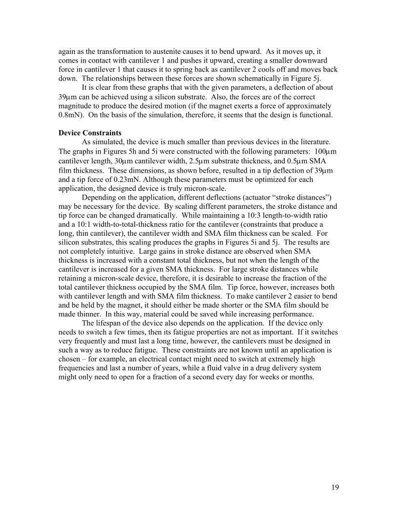
again as the transformation to austenite causes it to bend upward. As it moves up, it comes in contact with cantilever 1 and pushes it upward, creating a smaller downward force in cantilever 1 that causes it to spring back as cantilever 2 cools off and moves back down. The relationships between these forces are shown schematically in Figure 5j.
It is clear from these graphs that with the given parameters, a deflection of about 39µm can be achieved using a silicon substrate. Also, the forces are of the correct magnitude to produce the desired motion (if the magnet exerts a force of approximately 0.8mN). On the basis of the simulation, therefore, it seems that the design is functional.
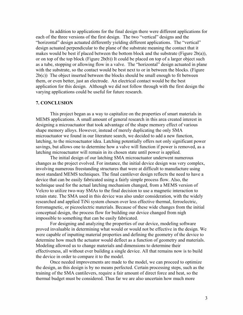
Device Constraints As simulated, the device is much smaller than previous devices in the literature. The graphs in Figures 5h and 5i were constructed with the following parameters: 100µm cantilever length, 30µm cantilever width, 2.5µm substrate thickness, and 0.5µm SMA film thickness. These dimensions, as shown before, resulted in a tip deflection of 39µm and a tip force of 0.23mN. Although these parameters must be optimized for each application, the designed device is truly micron-scale. Depending on the application, different deflections (actuator “stroke distances”) may be necessary for the device. By scaling different parameters, the stroke distance and tip force can be changed dramatically. While maintaining a 10:3 length-to-width ratio and a 10:1 width-to-total-thickness ratio for the cantilever (constraints that produce a long, thin cantilever), the cantilever width and SMA film thickness can be scaled. For silicon substrates, this scaling produces the graphs in Figures 5i and 5j. The results are not completely intuitive. Large gains in stroke distance are observed when SMA thickness is increased with a constant total thickness, but not when the length of the cantilever is increased for a given SMA thickness. For large stroke distances while retaining a micron-scale device, therefore, it is desirable to increase the fraction of the total cantilever thickness occupied by the SMA film. Tip force, however, increases both with cantilever length and with SMA film thickness. To make cantilever 2 easier to bend and be held by the magnet, it should either be made shorter or the SMA film should be made thinner. In this way, material could be saved while increasing performance. The lifespan of the device also depends on the application. If the device only needs to switch a few times, then its fatigue properties are not as important. If it switches very frequently and must last a long time, however, the cantilevers must be designed in such a way as to reduce fatigue. These constraints are not known until an application is chosen – for example, an electrical contact might need to switch at extremely high frequencies and last a number of years, while a fluid valve in a drug delivery system might only need to open for a fraction of a second every day for weeks or months.
19
Section 5 Figures
Non-latching Duty Cycle
0102030405060708090
100
0 10 20 30 40 50 60 70 80 90 100
Time Closed (%)
Cum
ulat
ive
Ener
gy C
onsu
med
(arb
. un
its)
Normally open Normally Closed
Max energy usage
Figure 5a: This graph shows the energy that is used when a actuator is held in its “switched” state.
Latching Duty Cycles
0
5
10
15
20
25
30
0 5 10 15
Each step equals one actuation
Cum
ulat
ive
Ener
gy C
onsu
med
(a
rb. u
nits
)
Low Power, Low Freq Low Power, High FreqHigh Power, Low Freq High Power, High Freq
Figure 5b: This graph shows the energy used when a latching model is used.
20
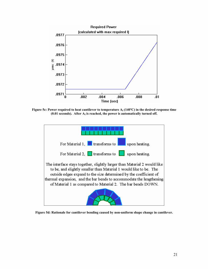
Figure 5c: Power required to heat cantilever to temperature Af (140ºC) in the desired response time (0.01 seconds). After Af is reached, the power is automatically turned off.
Figure 5d: Rationale for cantilever bending caused by non-uniform shape change in cantilever.
21

Figure 5e: Schematic drawing of bi-layered cantilever showing dimension notation (Chu, 1993). In the current project, material 2 is the SMA film and material 1 is the substrate.
22
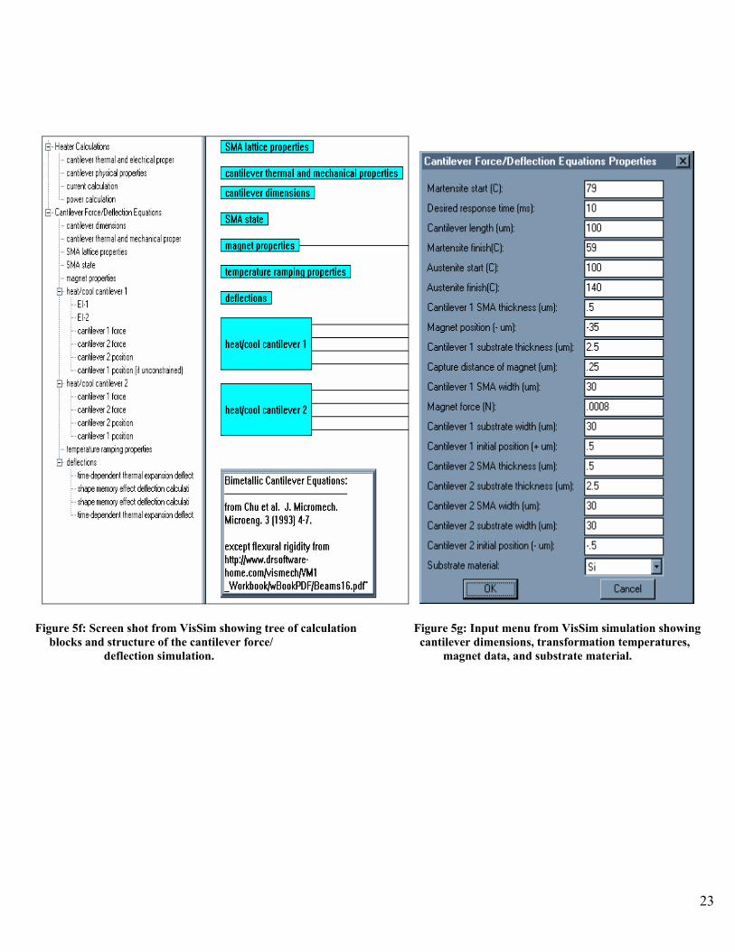
Figure 5f: Screen shot from VisSim showing tree of calculation Figure 5g: Input menu from VisSim simulation showing blocks and structure of the cantilever force/ cantilever dimensions, transformation temperatures,
deflection simulation. magnet data, and substrate material.
23
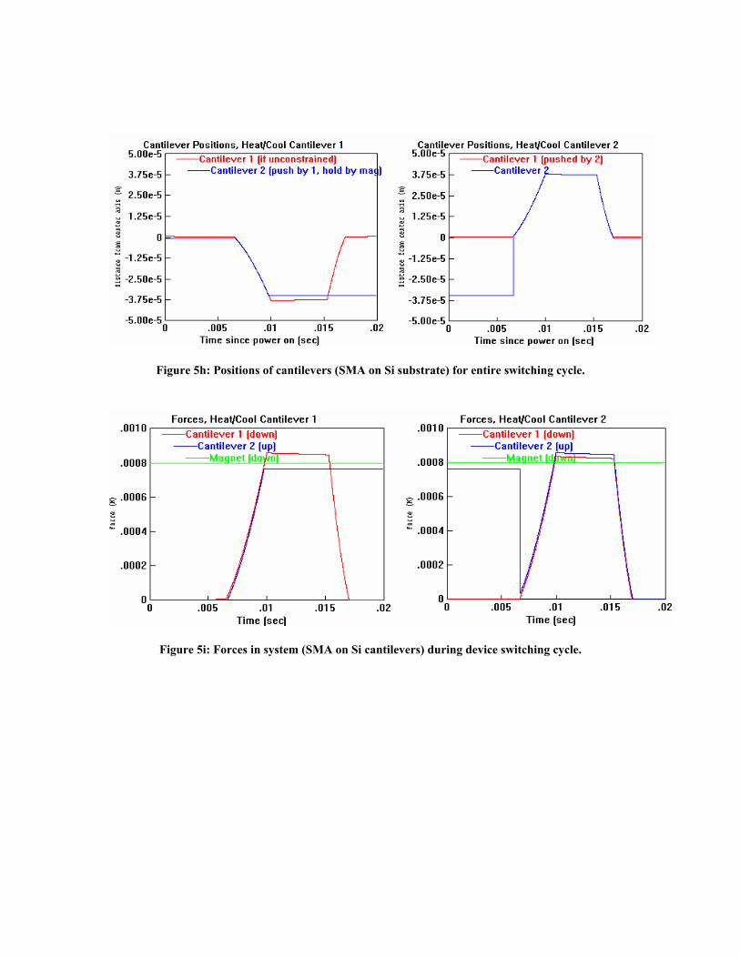
Figure 5h: Positions of cantilevers (SMA on Si substrate) for entire switching cycle.
Figure 5i: Forces in system (SMA on Si cantilevers) during device switching cycle.
Heating cantilever 1:
CANTILEVER 2F-cantilever 2 mart
F-cantilever 1 aust>
F-magnet
F-cantilever 2 mart>
CANTILEVER 2
F-cantilever 2 aust
F-cantilever 2 aust>
F-magnet
F-cantilever 1 mart>
Heating cantilever 2:
F-cantilever 1 aust
F-magnet
F-cantilever 1 mart
F-magnet
Figure 5j: Necessary relationships of forces in cantilever system.
Figure 5k: Cantilever tip deflection as a function of cantilever length and SMA film thickness, assuming a 10:3 length-to-width ratio and a 10:1 width-to-thickness ratio for the cantilever.
1
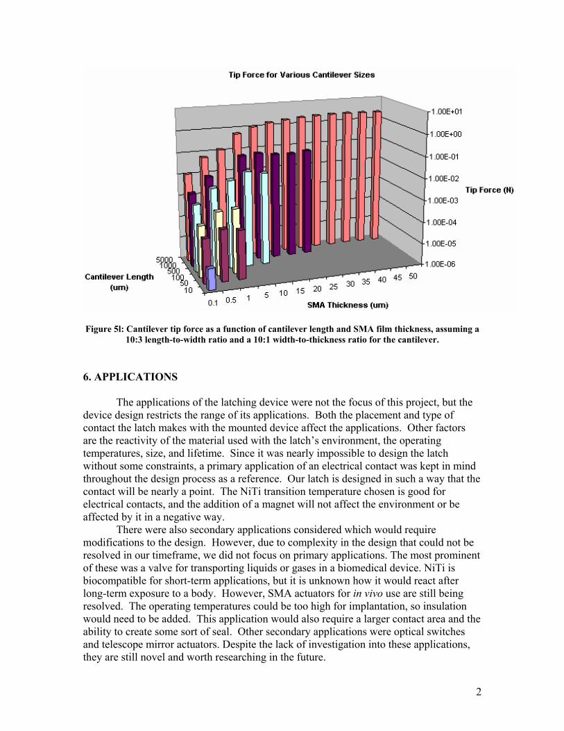
Figure 5l: Cantilever tip force as a function of cantilever length and SMA film thickness, assuming a 10:3 length-to-width ratio and a 10:1 width-to-thickness ratio for the cantilever.
6. APPLICATIONS
The applications of the latching device were not the focus of this project, but the device design restricts the range of its applications. Both the placement and type of contact the latch makes with the mounted device affect the applications. Other factors are the reactivity of the material used with the latch’s environment, the operating temperatures, size, and lifetime. Since it was nearly impossible to design the latch without some constraints, a primary application of an electrical contact was kept in mind throughout the design process as a reference. Our latch is designed in such a way that the contact will be nearly a point. The NiTi transition temperature chosen is good for electrical contacts, and the addition of a magnet will not affect the environment or be affected by it in a negative way. There were also secondary applications considered which would require modifications to the design. However, due to complexity in the design that could not be resolved in our timeframe, we did not focus on primary applications. The most prominent of these was a valve for transporting liquids or gases in a biomedical device. NiTi is biocompatible for short-term applications, but it is unknown how it would react after long-term exposure to a body. However, SMA actuators for in vivo use are still being resolved. The operating temperatures could be too high for implantation, so insulation would need to be added. This application would also require a larger contact area and the ability to create some sort of seal. Other secondary applications were optical switches and telescope mirror actuators. Despite the lack of investigation into these applications, they are still novel and worth researching in the future.
2
In addition to applications for the final design there were different applications for each of the three versions of the first design. The two “vertical” designs and the “horizontal” design actuated differently yielding different applications. The “vertical” design actuated perpendicular to the plane of the substrate meaning the contact that it makes would be best if placed between the bottom block and the substrate (Figure 2b(a)), or on top of the top block (Figure 2b(b)) It could be placed on top of a larger object such as a tube, stopping or allowing flow in a valve. The “horizontal” design actuated in plane with the substrate, so the contact would be best next to or in between the blocks. (Figure 2b(c)) The object inserted between the blocks should be small enough to fit between them, or even better, just an electrode. An electrical contact would be the best application for this design. Although we did not follow through with the first design the varying applications could be useful for future research. 7. CONCLUSION
This project began as a way to capitalize on the properties of smart materials in MEMS applications. A small amount of general research in this area created interest in designing a microactuator that took advantage of the shape memory effect of various shape memory alloys. However, instead of merely duplicating the only SMA microactuator we found in our literature search, we decided to add a new function, latching, to the microactuator idea. Latching potentially offers not only significant power savings, but allows one to determine how a valve will function if power is removed, as a latching microactuator will remain in its chosen state until power is applied.
The initial design of our latching SMA microactuator underwent numerous changes as the project evolved. For instance, the initial device design was very complex, involving numerous freestanding structures that were at difficult to manufacture using most standard MEMS techniques. The final cantilever design reflects the need to have a device that can be easily fabricated using a fairly simple process flow. Also, the technique used for the actual latching mechanism changed, from a MEMS version of Velcro to utilize two-way SMAs to the final decision to use a magnetic interaction to retain state. The SMA used in this device was also under consideration, with the widely researched and applied TiNi system chosen over less effective thermal, ferroelectric, ferromagnetic, or piezoelectric materials. Because of these wide changes from the initial conceptual design, the process flow for building our device changed from nigh impossible to something that can be easily fabricated.
For designing and analyzing the properties of our device, modeling software proved invaluable in determining what would or would not be effective in the design. We were capable of inputting material properties and defining the geometry of the device to determine how much the actuator would deflect as a function of geometry and materials. Modeling allowed us to change materials and dimensions to determine their effectiveness, all without ever building a single device. All that remains now is to build the device in order to compare it to the model.
Once needed improvements are made to the model, we can proceed to optimize the design, as this design is by no means perfected. Certain processing steps, such as the training of the SMA cantilevers, require a fair amount of direct force and heat, so the thermal budget must be considered. Thus far we are also uncertain how much more
3

energy efficient this design is compared to the current state of the art, and whether or not the actuator is capable of high operational frequency. These necessary improvements lead to the future work this project requires to bring this product to market. Once the device specifications have been set forward, the design and process flow can be completed and the device built. Experimental testing of the device will allow for several key aspects we were unable to complete during the design process. First, SMA thin film properties are not adequately described in the literature. Key materials aspects such as the Young’s modulus of thin films as well as fatigue measurements are sorely lacking. We used the bulk moduli in the simulation and experimental testing will demonstrate just how accurate these numbers are. Also, the key selling point of our design, low power consumption due to the latching function, is still in question. As described in the duty cycle section, our design offers the most power savings for low frequency switching with a low activation cost. So far, we are also uncertain how quickly the device will cool, which is the determining factor in the frequency of operation. These factors determine which applications the device is suitable for. As an example, a circuit breaker will be effective, but electrical switching may require higher frequencies than this device can handle. Essentially, we cannot evaluate out device fully until the device is actually built. We have designed a latching shape memory alloy microactuator that offers power savings and new functionality over the current state of the art MEMS microactuator. Using modeling software we were able to compare different design dimensions and materials choices without resorting to costly, time-consuming experimental testing. What remains is to build and optimize the design and account for any variables and considerations that escaped our modeling. We believe this design advances the state of the art in MEMS actuators and capitalizes on the properties of smart materials.
4
8. REFERENCES
Bhattacharyya, A., Faulkner, M.G., & Amalraj, J.J. (2000). Finite element modeling of cyclic thermal response of shape memory alloy wires with variable material properties. Computational Materials Science, 17(1), 93-104.
Chu, W.-H. et al. (1993). “Analysis of tip deflection and force of a bimetallic cantilever
microactuator.” J. Micromech. Microeng. 3, 4-7. “Definition of a Shape Memory Alloy.” Smart Lab Texas A&M.
http://smart.tamu.edu/overview/smaintro/simple/definition.html (Nov 10, 2002). “Definition of a Valve.” Plast-O-Matic Valves, Inc.
http://www.plastomatic.com/definition.html (Nov 10, 2002).
Foutz, Jerrold. “Switching Mode Power Supply Expert System.” SMPS Technology Knowledge Base. http://www.smpstech.com/exp/pwm022.htm (August 10, 001).
Frantz, N., Dufour-Gergam, E., Grandchamp, J.P., Bosseboeuf, A., Seiler, W., Nouet, G.,
et al. (2002). Shape memory thin films with transition above room temperature from Ni-rich NiTi films. Sensors and Actuators A: Physical, 99(1-2), 59-63.
Fu, Y., & Du, H. (in press). RF magnetron sputtered TiNiCu shape memory alloy thin
film. Materials Science and Engineering A. Galhotra, V. et al. “Shape Memory Alloy Based Micro Actuators.”
ACTUATOR 2000 TiNi Alloy Co., San Leandro, CA, 2000.
Huang, W. (1999). “‘Yield’ surfaces of shape memory alloys and their applications.” Acta Materialia. 47, 2769-2776.
Huang, W. (2002). On the selection of shape memory alloys for actuators. Materials & Design, 23(1), 11-19.
Gabry, B., Lexcellent, C., No, V.H., & Miyazaki, S. (2000). Thermodynamic modeling of
the recovery strains of sputter-deposited shape memory alloys Ti-Ni and Ti-Ni-Cu thin films. Thin Solid Films, 372(1-2), 118-133.
Gill, J., Chang, D., Momoda, L., & Carman, G. (2001). Manufacturing issues of thin film
NiTi microwrapper. Sensors and Actuators A: Physical, 93(2), 148-156. Gu, H.D., You, L., Leung, K.M., Chung, C.Y., Chan, K.S., & Lai, J.K.L. (1998). Growth
of TiNiHf shape memory alloy thin films by laser ablation of composite targets. Applied Surface Science, 127-129, 579-583.
5
6
Kakeshita, Tomoyuki and Otsuka, Kazuhiro. Science and
Technology of Shape-Memory Alloys: New Developments. MRS Bulletin, February 2002.
Kohl, M., Dittmann, D., Quandt, E., & Winzek, B. (2000). Thin film shape memory
microvalveswith adjustable operation temperature. Sensors and Actuators A: Physical, 83(1-3), 214-219.
Lin-Eftekhar, Judy. “Materials on the Move: Engineering Smart Materials.” UCLA
Engineer, http://www.seasalum.ucla.edu/smartmat.cfm, Spring 2002. Manfred Wuttig, University of Maryland Professor, private
discussion, November 2002. Mori, K., Li, J., Roytburd, A., Wuttig, M. (2002). Patterned Shape Memory Alloys.
Materials Transactions, JIM, 43(5), 951-955. Quanmin Su, S.Z. Hua and Manfred Wuttig, Proc. "Shape Memory Alloys", Trans. Mat.
Res. Soc. Jpn., 18B, 1057 (1994). Ren, M.H., Wang, L., Xu, D., and Cai, B.C. (2000). Sputter-deposited Ti-Ni-Cu shaped
memory alloy thin films. Materials & Design, 21(6), 583-586. Senturia, Steven D. Microsystem Design. Kluwer Academic
Publishers, Norwell, Massachusetts, 2001. Surbled, P., Clerc, C., Le Pioufle, B., Ataka, M., & Fujita, H. (2001). Effect of the
composition and thermal annealing on the transformation temperatures of sputtered TiNi shape memory alloy thin films. Thin Solid Films, 401(1-2), 52-59.


![arXiv:1111.2510v1 [cond-mat.soft] 10 Nov 2011 · combined with the temperature-dependent swelling properties of PNIPAM, allow us to use the polymer brush as a microactuator which](https://img.pdfslide.us/doc/110x75/5ec85ce651d9ea1b525a7b93/arxiv11112510v1-cond-matsoft-10-nov-2011-combined-with-the-temperature-dependent.jpg)