Embed Size (px)
Citation preview
SGM8631/2/3
6MHz, Rail-to-Rail I/O CMOS Operational Amplifiers
PRODUCT DESCRIPTION The SGM8631 (single), SGM8632 (dual) and SGM8633 (single with shutdown) are low noise, low voltage, and low power operational amplifiers that can be designed into a wide range of applications. The SGM8631/2/3 have a high gain-bandwidth product of 6MHz and a slew rate of 3.7V/μs. The SGM8633 has a power-down disable feature that reduces the supply current to less than 1μA. The SGM8631/2/3 are designed to provide optimal performance in low voltage and low noise systems. They provide rail-to-rail output swing into heavy loads. The input common mode voltage range includes ground, and the maximum input offset voltage is 3.5mV for SGM8631/2/3. They are specified over the extended industrial temperature range (-40℃ to +125℃). The
operating supply range is from 2V to 5.5V. The SGM8631 single is available in Green SC70-5, SOT-23-5 and SOIC-8 packages. The SGM8632 dual is available in Green SOIC-8 and MSOP-8 packages. The SGM8633 single with shutdown is available in Green SOT-23-6 and SOIC-8 packages.
FEATURES Rail-to-Rail Input and Output
3.5mV Maximum VOS High Gain-Bandwidth Product: 6MHz High Slew Rate: 3.7V/μs Settling Time to 0.1% with 2V Step: 0.5μs Overload Recovery Time: 0.9μs Low Noise: 13nV/ Hz at 1kHz
Supply Voltage Range: 2V to 5.5V Input Voltage Range: -0.1V to +5.6V with VS = 5.5V Low Supply Current
SGM8631/3: 570μA (TYP) SGM8632: 480μA/Amplifier (TYP) Less than 1μA Shutdown Current for SGM8633
Small Packaging SGM8631 Available in Green SC70-5, SOT-23-5 and SOIC-8 SGM8632 Available in Green MSOP-8 and SOIC-8 SGM8633 Available in Green SOT-23-6 and SOIC-8
APPLICATIONS Sensors Audio Active Filters A/D Converters Communications Test Equipment Cellular and Cordless Phones Laptops and PDAs Photodiode Amplification Battery-Powered Instrumentation
REV. C. 3 SG Micro Corp
www.sg-micro.com

6MHz, Rail-to-Rail I/O SGM8631/2/3 CMOS Operational Amplifiers
PACKAGE/ORDERING INFORMATION
MODEL PACKAGE DESCRIPTION
SPECIFIED TEMPERATURE
RANGE ORDERING NUMBER
PACKAGE MARKING
PACKING OPTION
SGM8631
SC70-5 -40℃ to +125℃ SGM8631XC5/TR 8631 Tape and Reel, 3000
SOT-23-5 -40℃ to +125℃ SGM8631XN5/TR 8631 Tape and Reel, 3000
SOIC-8 -40℃ to +125℃ SGM8631XS/TR SGM8631XS XXXXX Tape and Reel, 2500
SGM8632 MSOP-8 -40℃ to +125℃ SGM8632XMS/TR
SGM8632 XMS
XXXXX Tape and Reel, 3000
SOIC-8 -40℃ to +125℃ SGM8632XS/TR SGM8632XS XXXXX Tape and Reel, 2500
SGM8633 SOT-23-6 -40℃ to +125℃ SGM8633XN6/TR 8633 Tape and Reel, 3000
SOIC-8 -40℃ to +125℃ SGM8633XS/TR SGM8633XS XXXXX Tape and Reel, 2500
NOTE: XXXXX = Date Code and Vendor Code. Green (RoHS & HSF): SG Micro Corp defines "Green" to mean Pb-Free (RoHS compatible) and free of halogen substances. If you have additional comments or questions, please contact your SGMICRO representative directly. ABSOLUTE MAXIMUM RATINGS Supply Voltage, +VS to -VS ................................................ 6V Input Common Mode Voltage Range .................................................... (-VS) - 0.3V to (+VS) + 0.3V Storage Temperature Range ........................ -65℃ to +150℃ Junction Temperature ................................................. +150℃ Package Thermal Resistance @ TA = 25℃ SC70-5, θJA .............................................................. 333℃/W SOT-23-5, θJA .......................................................... 190℃/W SOT-23-6, θJA .......................................................... 190℃/W SOIC-8, θJA .............................................................. 125℃/W MSOP-8, θJA ............................................................ 216℃/W Lead Temperature (Soldering 10sec) .................................................................................... +260℃ ESD Susceptibility HBM (SGM8631/2) ...................................................... 8000V HBM (SGM8633) ......................................................... 4000V MM ................................................................................. 400V CDM ............................................................................ 1000V RECOMMENDED OPERATING CONDITIONS Operating Temperature Range ..................... -40℃ to +125℃
OVERSTRESS CAUTION Stresses beyond those listed may cause permanent damage to the device. Functional operation of the device at these or any other conditions beyond those indicated in the operational section of the specification is not implied. Exposure to absolute maximum rating conditions for extended periods may affect reliability. ESD SENSITIVITY CAUTION This integrated circuit can be damaged by ESD if you don’t pay attention to ESD protection. SGMICRO recommends that all integrated circuits be handled with appropriate precautions. Failure to observe proper handling and installation procedures can cause damage. ESD damage can range from subtle performance degradation to complete device failure. Precision integrated circuits may be more susceptible to damage because very small parametric changes could cause the device not to meet its published specifications. DISCLAIMER SG Micro Corp reserves the right to make any change in circuit design, specification or other related things if necessary without notice at any time.
SG Micro Corp
www.sg-micro.com 2

6MHz, Rail-to-Rail I/O SGM8631/2/3 CMOS Operational Amplifiers
PIN CONFIGURATIONS SGM8631 (TOP VIEW) SGM8631/8633 (TOP VIEW)
+VS
-IN3 4
51
2
OUT
-VS
+IN
(SGM8633 ONLY)
-IN
+IN
-VS
NC
5
6
7
81
2
3
4
+VS
NC
OUT
DISABLE
NC = NO CONNECT
SC70-5/SOT-23-5 SOIC-8
SGM8633 (TOP VIEW) SGM8632 (TOP VIEW)
OUT
3 4
5
61
2-VS
+IN
+VS
DISABLE
-IN
OUTA
+INA
OUTB
+VS
+INB5
6
7
81
2
3
4
-INA
-VS
-INB
SOT-23-6 SOIC-8/MSOP-8
SG Micro Corp
www.sg-micro.com 3

6MHz, Rail-to-Rail I/O SGM8631/2/3 CMOS Operational Amplifiers
ELECTRICAL CHARACTERISTICS (At TA = +25℃, VS = +5V, VCM = VS/2, RL = 600Ω, unless otherwise noted.)
PARAMETER CONDITIONS
SGM8631/2/3
TYP MIN/MAX OVER TEMPERATURE
+25℃ +25℃ -40℃ to
+85℃
-40℃ to
+125℃ UNITS MIN/
MAX
INPUT CHARACTERISTICS
Input Offset Voltage (VOS) 0.9 3.5 3.7 3.8 mV MAX
Input Bias Current (IB) 1 pA TYP
Input Offset Current (IOS) 1 pA TYP Input Common Mode Voltage Range (VCM) VS = 5.5V -0.1 to 5.6 V TYP
Common Mode Rejection Ratio (CMRR)
VS = 5.5V, VCM = -0.1V to 4V 84 68 67 66 dB MIN
VS = 5.5V, VCM = -0.1V to 5.6V 76 dB MIN
Open-Loop Voltage Gain (AOL) RL = 600Ω, VO = 0.15V to 4.85V 86 79 73 69 dB MIN
RL = 10kΩ , VO = 0.05V to 4.95V 103 dB MIN
Input Offset Voltage Drift (ΔVOS/ΔT) 2.4 μV/℃ TYP
OUTPUT CHARACTERISTICS
Output Voltage Swing from Rail RL = 600Ω 0.079 V TYP
RL = 10kΩ 0.007 V TYP
Output Current (IOUT) 58 40 30 26 mA MIN
Closed-Loop Output Impedance f = 200kHz, G = 1 5.4 Ω TYP
POWER-DOMN DISABLE (SGM8633 ONLY)
Turn-On Time 1.3 μs TYP
Turn-Off Time 0.4 μs TYP
DISABLE Voltage-Off 0.8 V MAX
DISABLE Voltage-On 2 V MIN
POWER SUPPLY
Operating Voltage Range 2 2 2 2 V MIN
5.5 5.5 5.5 5.5 V MAX
Power Supply Rejection Ratio (PSRR) VS = 2V to 5.5V, VCM = (-VS) + 0.5V 84 69 68 67 dB MIN
Quiescent Current/ Amplifier (IQ)
SGM8632 IOUT = 0 480 620 720 790 μA MAX
SGM8631/3 IOUT = 0 570 720 820 880 μA MAX Supply Current when Disabled (SGM8633 only) 0.5 8 9 10 μA MAX
DYNAMIC PERFORMANCE
Gain-Bandwidth Product (GBP) 6 MHz TYP
Phase Margin (φO) 63 ° TYP
Full Power Bandwidth (BWP) <1% distortion 250 kHz TYP
Slew Rate (SR) G=1, 2V output step 3.7 V/μs TYP
Settling Time to 0.1% (tS) G=1, 2V output step 0.5 μs TYP
Overload Recovery Time VIN × Gain = VS 0.9 μs TYP
NOISE PERFORMANCE
Voltage Noise Density (en) f = 1kHz 13 nV/ Hz TYP
SG Micro Corp
www.sg-micro.com 4
6MHz, Rail-to-Rail I/O SGM8631/2/3 CMOS Operational Amplifiers
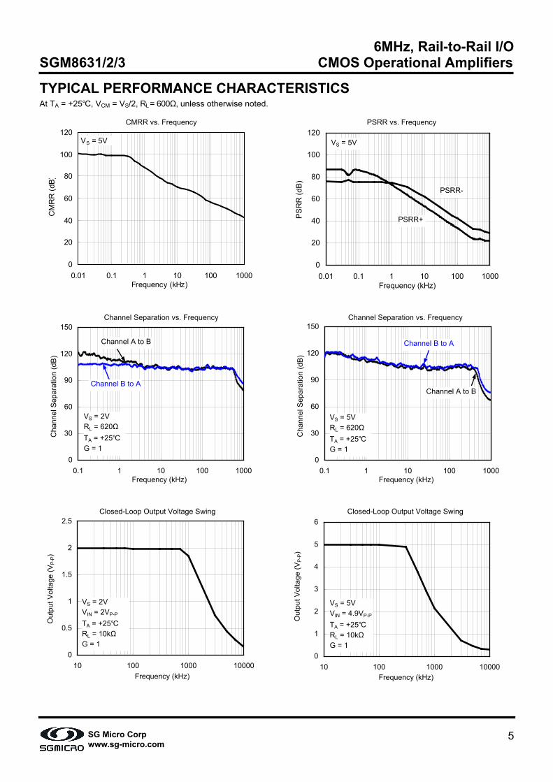
TYPICAL PERFORMANCE CHARACTERISTICS At TA = +25℃, VCM = VS/2, RL = 600Ω, unless otherwise noted.
CMRR vs. Frequency PSRR vs. Frequency
0
20
40
60
80
100
120
0.01 0.1 1 10 100 1000Frequency (kHz)
CM
RR
(dB)
VS = 5V
0
20
40
60
80
100
120
0.01 0.1 1 10 100 1000Frequency (kHz)
PS
RR
(dB
)
VS = 5V
PSRR+
PSRR-
Channel Separation vs. Frequency Channel Separation vs. Frequency
0
30
60
90
120
150
0.1 1 10 100 1000Frequency (kHz)
Cha
nnel
Sep
arat
ion
(dB
)
VS = 2VRL = 620ΩTA = +25℃G = 1
Channel B to A
Channel A to B
0
30
60
90
120
150
0.1 1 10 100 1000Frequency (kHz)
Cha
nnel
Sep
arat
ion
(dB
)
VS = 5VRL = 620ΩTA = +25℃G = 1
Channel A to B
Channel B to A
Closed-Loop Output Voltage Swing Closed-Loop Output Voltage Swing
0
0.5
1
1.5
2
2.5
10 100 1000 10000Frequency (kHz)
Out
put V
olta
ge (V
P-P)
VS = 2VVIN = 2VP-P
TA = +25℃RL = 10kΩG = 1
0
1
2
3
4
5
6
10 100 1000 10000Frequency (kHz)
Out
put V
olta
ge (V
P-P)
VS = 5VVIN = 4.9VP-P
TA = +25℃RL = 10kΩG = 1
SG Micro Corp
www.sg-micro.com 5

6MHz, Rail-to-Rail I/O SGM8631/2/3 CMOS Operational Amplifiers
TYPICAL PERFORMANCE CHARACTERISTICS At TA = +25℃, VCM = VS/2, RL = 600Ω, unless otherwise noted.
Small-Signal Overshoot vs. Load Capacitance Small-Signal Overshoot vs. Load Capacitance
0
10
20
30
40
50
10 100 1000Load Capacitance (pF)
Sm
all-S
igna
l Ove
rsho
ot (%
)
VS = 2VRL = 10kΩTA = +25℃G = 1
0
10
20
30
40
50
10 100 1000Load Capacitance (pF)
Sm
all-S
igna
l Ove
rsho
ot (%
)
VS = 5VRL = 10kΩTA = +25℃G = 1
Output Impedance vs. Frequency Output Impedance vs. Frequency
0
20
40
60
80
100
1 10 100 1000 10000Frequency (kHz)
Out
put I
mpe
danc
e (Ω
)
VS = 2V
G = 10 G = 1
G = 100
0
20
40
60
80
100
1 10 100 1000 10000Frequency (kHz)
Out
put I
mpe
danc
e (Ω
)
VS = 5V
G = 10G = 1
G = 100
Large-Signal Step Response Large-Signal Step Response
Time (400ns/div)
Vol
tage
(1V
/div
)
G = 1CL = 100pFRL = 10kΩVS = 2V
Time (400ns/div)
Vol
tage
(1V
/div
)
G = 1CL = 100pFRL = 10kΩVS = 5V
SG Micro Corp
www.sg-micro.com 6

6MHz, Rail-to-Rail I/O SGM8631/2/3 CMOS Operational Amplifiers
TYPICAL PERFORMANCE CHARACTERISTICS At TA = +25℃, VCM = VS/2, RL = 600Ω, unless otherwise noted.
Small-Signal Step Response Small-Signal Step Response
Time (1μs/div)
Vol
tage
(50m
V/d
iv) G = 1
CL = 100pFRL = 10kΩVS = 2V
Time ((1μs/div)
Vol
tage
(50m
V/d
iv) G = 1
CL = 100pFRL = 10kΩVS = 5V
Positive overload Recovery Negative Overload Recovery
Time (1µs/div)
0V
VIN
0V
VOUT
50mV
/div1V
/div
VS = 5VVIN = 50mVRL = 620ΩG = -100
Time (1µs/div)
0V
VIN
0V
VOUT
50mV
/div1V
/div
VS = 5VVIN = 50mVRL = 620ΩG = -100
Supply Current vs. Temperature Shutdown Current vs. Temperature
0.3
0.4
0.5
0.6
0.7
0.8
-50 -25 0 25 50 75 100 125
Temperature (℃)
Sup
ply
Cur
rent
(mA
)
VS = 3V
VS = 2V
VS = 5V
0
150
300
450
600
750
-50 -25 0 25 50 75 100 125
Temperature (℃)
Shu
tdow
n C
urre
nt (n
A)
VS = 5V
VS = 3VVS = 2V
SG Micro Corp
www.sg-micro.com 7

6MHz, Rail-to-Rail I/O SGM8631/2/3 CMOS Operational Amplifiers
TYPICAL PERFORMANCE CHARACTERISTICS At TA = +25℃, VCM = VS/2, RL = 600Ω, unless otherwise noted.
CMRR vs. Temperature PSRR vs. Temperature
50
60
70
80
90
100
110
-50 -25 0 25 50 75 100 125Temperature (℃)
CM
RR
(dB
)
VCM = -0.1V to 4V
VS = 5.5V
VCM = -0.1V to 5.6V
50
60
70
80
90
100
110
-50 -25 0 25 50 75 100 125Temperature (℃)
PS
RR
(dB
)
VS = 2V to 5.5V
Open-Loop Voltage Gain vs. Temperature Open-Loop Voltage Gain vs. Temperature
70
80
90
100
110
120
-50 -25 0 25 50 75 100 125Temperature (℃)
Ope
n–Lo
op V
olta
ge G
ain
(dB
)
VS = 5V
RL = 10kΩVS = 2V
60
70
80
90
100
110
-50 -25 0 25 50 75 100 125Temperature (℃)
Ope
n–Lo
op V
olta
ge G
ain
(dB
)
VS = 5V
RL = 600Ω
VS = 2V
Output Voltage Swing vs. Output Current Output Voltage Swing vs. Output Current
0
1
2
3
4
5
0 10 20 30 40 50 60 70 80Output Current (mA)
Out
put V
olta
ge (V
)
Sourcing Current
Sinking Current
-40℃
+25℃
+125℃
VS = 5V
0
0.5
1
1.5
2
0 5 10 15 20 25 30 35Output Current (mA)
Out
put V
olta
ge (V
)
Sourcing Current
Sinking Current
-40℃
+25℃+125℃
VS = 2V
SG Micro Corp
www.sg-micro.com 8

6MHz, Rail-to-Rail I/O SGM8631/2/3 CMOS Operational Amplifiers
TYPICAL PERFORMANCE CHARACTERISTICS At TA = +25℃, VCM = VS/2, RL = 600Ω, unless otherwise noted.
Input Voltage Noise Spectral Density vs. Frequency Offset Voltage Production Distribution
1
10
100
1000
10 100 1000 10000Frequency (Hz)
Vol
tage
Noi
se (n
V/√
Hz)
VS = 5V
0
5
10
15
20
25
30
35
-4 -3 -2 -1 0 1 2 3 4Offset Voltage (mV)
Per
cent
age
of A
mpl
ifier
s (%
)
20300 Samples1 Production Lot
VS = 5V
SG Micro Corp
www.sg-micro.com 9

6MHz, Rail-to-Rail I/O SGM8631/2/3 CMOS Operational Amplifiers
APPLICATION NOTES Driving Capacitive Loads The SGM8631/2/3 can directly drive 1000pF in unity-gain without oscillation. The unity-gain follower (buffer) is the most sensitive configuration to capacitive loading. Direct capacitive loading reduces the phase margin of amplifiers and this results in ringing or even oscillation. Applications that require greater capacitive driving capability should use an isolation resistor between the output and the capacitive load like the circuit in Figure 1. The isolation resistor RISO and the load capacitor CL form a zero to increase stability. The bigger the RISO resistor value, the more stable VOUT will be. Note that this method results in a loss of gain accuracy because RISO forms a voltage divider with the RLOAD.
VIN
VOUTSGM8631CL
RISO
Figure 1. Indirectly Driving Heavy Capacitive Load An improved circuit is shown in Figure 2. It provides DC accuracy as well as AC stability. RF provides the DC accuracy by connecting the inverting input with the output. CF and RISO serve to counteract the loss of phase margin by feeding the high frequency component of the output signal back to the amplifier’s inverting input, thereby preserving phase margin in the overall feedback loop.
VIN
VOUTSGM8631
CL
RISO
RL
RF
CF
Figure 2. Indirectly Driving Heavy Capacitive Load with DC Accuracy For non-buffer configuration, there are two other ways to increase the phase margin: (a) by increasing the amplifier’s closed-loop gain or (b) by placing a capacitor in parallel with the feedback resistor to counteract the parasitic capacitance associated with inverting node.
Power-Supply Bypassing and Layout The SGM8631/2/3 family operates from either a single +2V to +5.5V supply or dual ±1V to ±2.75V supplies. For single-supply operation, bypass the power supply +VS with a 0.1µF ceramic capacitor which should be placed close to the +VS pin. For dual-supply operation, both the +VS and the -VS supplies should be bypassed to ground with separate 0.1µF ceramic capacitors. 2.2µF tantalum capacitor can be added for better performance. Good PC board layout techniques optimize performance by decreasing the amount of stray capacitance at the op amp’s inputs and output. To decrease stray capacitance, minimize trace lengths and widths by placing external components as close to the device as possible. Use surface-mount components whenever possible. For the operational amplifier, soldering the part to the board directly is strongly recommended. Try to keep the high frequency current loop area small to minimize the EMI (electromagnetic interfacing).
SGM8631
+VS
Vn
Vp
-VS
VOUT
10µF
0.1µF
10µF
0.1µF
SGM8631
Vn
Vp
+VS
-VS (GND)
VOUT
10µF
0.1µF
Figure 3. Amplifier with Bypass Capacitors Grounding A ground plane layer is important for SGM8631/2/3 circuit design. The length of the current path in an inductive ground return will create an unwanted voltage noise. Broad ground plane areas will reduce the parasitic inductance. Input-to-Output Coupling To minimize capacitive coupling, the input and output signal traces should not be in parallel. This helps reduce unwanted positive feedback.
SG Micro Corp
www.sg-micro.com 10

6MHz, Rail-to-Rail I/O SGM8631/2/3 CMOS Operational Amplifiers
TYPICAL APPLICATION CIRCUITS Differential Amplifier The circuit shown in Figure 4 performs the difference function. If the resistor ratios are equal (R4/R3 = R2/R1), then VOUT = (Vp - Vn) × R2/R1 + VREF.
Vn
Vp
VOUTSGM8631
VREF
R1
R2
R3
R4
Figure 4. Differential Amplifier Instrumentation Amplifier The circuit in Figure 5 performs the same function as that in Figure 4 but with a high input impedance.
Vn
Vp
SGM8631
VREF
R1
R2
R3 R4
VOUT
SGM8631
SGM8631
Figure 5. Instrumentation Amplifier
Low-Pass Active Filter The low-pass filter shown in Figure 6 has a DC gain of (-R2/R1) and the -3dB corner frequency is 1/2πR2C. Make sure the filter bandwidth is within the bandwidth of the amplifier. The large values of feedback resistors can couple with parasitic capacitance and cause undesired effects such as ringing or oscillation in high-speed amplifiers. Keep resistor values as low as possible and consistent with output loading consideration.
VIN
VOUTSGM8631
R1R2
R3 = R1 // R2
C
Figure 6. Low-Pass Active Filter
SG Micro Corp
www.sg-micro.com 11

PACKAGE INFORMATION
SG Micro Corp www.sg-micro.com
TX00043.000
PACKAGE OUTLINE DIMENSIONS
SC70-5
e
e1
E1 E
D
b
A
A2
A1
L
cθ0.20
L1
RECOMMENDED LAND PATTERN (Unit: mm)
1.9
0.65
1.3
0.75
0.4
Dimensions In Millimeters
Dimensions In Inches Symbol
MIN MAX MIN MAX
A 0.900 1.100 0.035 0.043
A1 0.000 0.100 0.000 0.004
A2 0.900 1.000 0.035 0.039
b 0.150 0.350 0.006 0.014
c 0.080 0.150 0.003 0.006
D 2.000 2.200 0.079 0.087
E 1.150 1.350 0.045 0.053
E1 2.150 2.450 0.085 0.096
e 0.65 TYP 0.026 TYP
e1 1.300 BSC 0.051 BSC
L 0.525 REF 0.021 REF
L1 0.260 0.460 0.010 0.018
θ 0° 8° 0° 8°

PACKAGE INFORMATION
SG Micro Corp www.sg-micro.com
TX00033.000
PACKAGE OUTLINE DIMENSIONS
SOT-23-5
EE1
e
e1
b
D
A1
A2
A
c
L
θ0.2
RECOMMENDED LAND PATTERN (Unit: mm)
1.90
2.59
0.99
0.69 0.95
Dimensions In Millimeters
Dimensions In Inches Symbol
MIN MAX MIN MAX
A 1.050 1.250 0.041 0.049
A1 0.000 0.100 0.000 0.004
A2 1.050 1.150 0.041 0.045
b 0.300 0.500 0.012 0.020
c 0.100 0.200 0.004 0.008
D 2.820 3.020 0.111 0.119
E 1.500 1.700 0.059 0.067
E1 2.650 2.950 0.104 0.116
e 0.950 BSC 0.037 BSC
e1 1.900 BSC 0.075 BSC
L 0.300 0.600 0.012 0.024
θ 0° 8° 0° 8°

PACKAGE INFORMATION
SG Micro Corp www.sg-micro.com
TX00010.000
PACKAGE OUTLINE DIMENSIONS
SOIC-8
D
EE1
e
b
A
A2
A1 c
L
θ
1.27
0.6
2.2
5.2
RECOMMENDED LAND PATTERN (Unit: mm)
Dimensions In Millimeters
Dimensions In Inches Symbol
MIN MAX MIN MAX
A 1.350 1.750 0.053 0.069
A1 0.100 0.250 0.004 0.010
A2 1.350 1.550 0.053 0.061
b 0.330 0.510 0.013 0.020
c 0.170 0.250 0.006 0.010
D 4.700 5.100 0.185 0.200
E 3.800 4.000 0.150 0.157
E1 5.800 6.200 0.228 0.244
e 1.27 BSC 0.050 BSC
L 0.400 1.270 0.016 0.050
θ 0° 8° 0° 8°

PACKAGE INFORMATION
SG Micro Corp www.sg-micro.com
TX00014.000
PACKAGE OUTLINE DIMENSIONS
MSOP-8
E1 E
e
D
A1
L
c
A
A2θ
b
RECOMMENDED LAND PATTERN (Unit: mm)
1.02
0.41 0.65
4.8
Dimensions In Millimeters
Dimensions In Inches Symbol
MIN MAX MIN MAX
A 0.820 1.100 0.032 0.043
A1 0.020 0.150 0.001 0.006
A2 0.750 0.950 0.030 0.037
b 0.250 0.380 0.010 0.015
c 0.090 0.230 0.004 0.009
D 2.900 3.100 0.114 0.122
E 2.900 3.100 0.114 0.122
E1 4.750 5.050 0.187 0.199
e 0.650 BSC 0.026 BSC
L 0.400 0.800 0.016 0.031
θ 0° 6° 0° 6°

PACKAGE INFORMATION
SG Micro Corp www.sg-micro.com
TX00034.000
PACKAGE OUTLINE DIMENSIONS
SOT-23-6
EE1
e
e1
b
D
A1
A2
A
c
L
θ0.2
2.59
0.99
0.950.69
RECOMMENDED LAND PATTERN (Unit: mm)
Dimensions In Millimeters
Dimensions In Inches Symbol
MIN MAX MIN MAX
A 1.050 1.250 0.041 0.049
A1 0.000 0.100 0.000 0.004
A2 1.050 1.150 0.041 0.045
b 0.300 0.500 0.012 0.020
c 0.100 0.200 0.004 0.008
D 2.820 3.020 0.111 0.119
E 1.500 1.700 0.059 0.067
E1 2.650 2.950 0.104 0.116
e 0.950 BSC 0.037 BSC
e1 1.900 BSC 0.075 BSC
L 0.300 0.600 0.012 0.024
θ 0° 8° 0° 8°

PACKAGE INFORMATION
SG Micro Corp www.sg-micro.com
TX10000.000
TAPE AND REEL INFORMATION NOTE: The picture is only for reference. Please make the object as the standard.
KEY PARAMETER LIST OF TAPE AND REEL
Package Type Reel
Diameter
Reel Width W1
(mm)
A0 (mm)
B0 (mm)
K0 (mm)
P0 (mm)
P1 (mm)
P2 (mm)
W (mm)
Pin1 Quadrant
SC70-5 7″ 9.5 2.25 2.55 1.20 4.0 4.0 2.0 8.0 Q3
SOT-23-5 7″ 9.5 3.2 3.2 1.4 4.0 4.0 2.0 8.0 Q3
SOT-23-6 7″ 9.5 3.17 3.23 1.37 4.0 4.0 2.0 8.0 Q3
SOIC-8 13″ 12.4 6.4 5.4 2.1 4.0 8.0 2.0 12.0 Q1
MSOP-8 13″ 12.4 5.2 3.3 1.5 4.0 8.0 2.0 12.0 Q1
DD
0001
Reel Width (W1)
Reel Diameter
REEL DIMENSIONS
TAPE DIMENSIONS
DIRECTION OF FEED
P2 P0
W
P1 A0 K0
B0Q1 Q2
Q4Q3 Q3 Q4
Q2Q1
Q3 Q4
Q2Q1

PACKAGE INFORMATION
SG Micro Corp www.sg-micro.com
TX20000.000
CARTON BOX DIMENSIONS
NOTE: The picture is only for reference. Please make the object as the standard.
KEY PARAMETER LIST OF CARTON BOX
Reel Type Length (mm)
Width (mm)
Height (mm)
Pizza/Carton
7″ (Option) 368 227 224 8
7″ 442 410 224 18
13″ 386 280 370 5
DD
0002