Embed Size (px)
Citation preview
NANOSTRUCTURED MATERIALS-PROCESSING, STRUCTURES, PROPERTIES AND APPLI CATIONS
Severe plastic deformation (SPD) and nanostructured materialsby machining
Srinivasan Swaminathan Æ M. Ravi Shankar Æ Balkrishna C. Rao ÆW. Dale Compton Æ Srinivasan Chandrasekar Æ Alexander H. King ÆKevin P. Trumble
Received: 30 May 2006 / Accepted: 31 July 2006 / Published online: 4 January 2007� Springer Science+Business Media, LLC 2006
Abstract Large plastic strains between 1 and 15 can be
imposed in chips formed by plane-strain (2-D) machin-
ing of metals and alloys. This approach has been used to
examine microstructure changes induced by large strain
deformation in model systems—copper and its alloys,
precipitation-hardenable aluminum alloys, high-
strength materials such as titanium, Inconel 718 and
52100 steel, and an amorphous alloy. It is shown that
materials with average grain sizes in the range of
60 nm–1 lm can be created by varying the parameters
of machining, which in turn affects the deformation
processes. Furthermore, a switch-over from an elon-
gated subgrain microstructure to an equi-axed nano-
crystalline microstructure, with a preponderance of
large-angle grain boundaries, has been demonstrated at
the higher levels of strain in several of these materials.
This switch-over can be readily controlled by varying
the deformation conditions. Dynamic recrystallization
has been demonstrated in select material systems under
particular conditions of strain and temperature. This
study may be seen as providing an important bridge
between furthering the understanding of microstruc-
tural refinement by large strain deformation and the
practical utilization of nanostructured materials in
structural and mechanical applications. Conventional
plane-strain machining has been shown to be a viable
SPD method for examining the underlying processes of
very large strain deformation.
Introduction
Interest in ultra-fine grained (UFG) materials, which
exhibit significantly enhanced mechanical properties,
has focused renewed attention on the use of severe
plastic deformation (SPD) as a means for achieving
microstructure refinement in metals and alloys. The
role of deformation in microstructure refinement is
best highlighted in the pioneering studies of Embury
and Fisher [1] on deformation of pearlite, and Lang-
ford and Cohen [2] on iron. Langford and Cohen [2],
for example, imposed large plastic strains in iron by
repeated passes of wire drawing and found the micro-
structure of the deformed iron wire to be composed of
grains and dislocation substructures with sizes in the
sub-micrometer range. Furthermore, there was a
significant increase in the flow stress of the wire. The
use of similar SPD approaches to realize and study
microstructure refinement has received an impetus in
recent years from the work of Segal et al. [3] and
others [4–7]. In these SPD approaches, large shear
strains (c ‡ 4) were imposed, by the cumulative appli-
cation of plastic deformation, using multiple passes of
deformation processing such as equal channel angular
extrusion (ECAE), drawing, rolling, or high-pressure
torsional straining (HPT). While these SPD methods
S. Swaminathan � B. C. Rao � W. D. Compton �S. Chandrasekar (&)Center for Materials Processing and Tribology, School ofIndustrial Engineering, Purdue University, West Lafayette,IN 47907, USAe-mail: [email protected]
M. Ravi ShankarDepartment of Industrial Engineering, University ofPittsburgh, Pittsburgh, PA 15261, USA
A. H. King � K. P. TrumbleSchool of Materials Engineering, Purdue University, WestLafayette, IN 47907, USA
J Mater Sci (2007) 42:1529–1541
DOI 10.1007/s10853-006-0745-9
123
are capable of producing bulk nanostructured materi-
als and have provided insights into mechanisms of
microstructure refinement, they possess some limita-
tions. First, multiple passes of deformation are needed
to create the large plastic strains. Second, moderate
and high-strength alloys are difficult to deform in this
manner at ambient temperature due to constraints
imposed by the forming equipment, including durabil-
ity of the tools and dies. Lastly, there are uncertainties
pertaining to knowledge and control of deformation
parameters.
An attractive route for imposing very large plastic
strains in a single pass of deformation, while overcom-
ing the aforementioned limitations, is the process of
chip formation by machining. Large plastic strains
experienced by a chip during its creation by machining
result in significant microstructure refinement, includ-
ing the creation of nanostructured materials [8–10].
This suggests an alternative SPD approach for studying
microstructure changes at the micro- and nano-scales.
We describe below important aspects of the large
strain deformation field in machining. The features of
this SPD approach are then illustrated by its applica-
tion to the study of formation of UFG and nanocrys-
talline microstructures in various alloys.
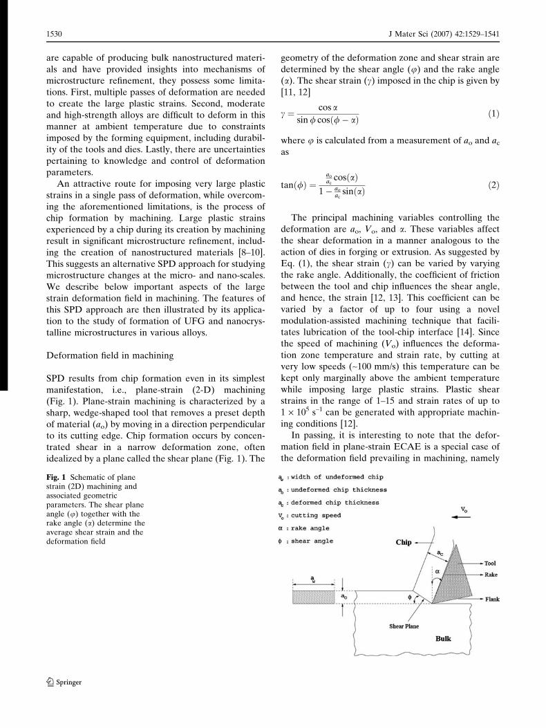
Deformation field in machining
SPD results from chip formation even in its simplest
manifestation, i.e., plane-strain (2-D) machining
(Fig. 1). Plane-strain machining is characterized by a
sharp, wedge-shaped tool that removes a preset depth
of material (ao) by moving in a direction perpendicular
to its cutting edge. Chip formation occurs by concen-
trated shear in a narrow deformation zone, often
idealized by a plane called the shear plane (Fig. 1). The
geometry of the deformation zone and shear strain are
determined by the shear angle (u) and the rake angle
(a). The shear strain (c) imposed in the chip is given by
[11, 12]
c ¼ cos asin / cosð/� aÞ ð1Þ
where u is calculated from a measurement of ao and ac
as
tanð/Þ ¼ao
accosðaÞ
1� ao
acsinðaÞ ð2Þ
The principal machining variables controlling the
deformation are ao, Vo, and a. These variables affect
the shear deformation in a manner analogous to the
action of dies in forging or extrusion. As suggested by
Eq. (1), the shear strain (c) can be varied by varying
the rake angle. Additionally, the coefficient of friction
between the tool and chip influences the shear angle,
and hence, the strain [12, 13]. This coefficient can be
varied by a factor of up to four using a novel
modulation-assisted machining technique that facili-
tates lubrication of the tool-chip interface [14]. Since
the speed of machining (Vo) influences the deforma-
tion zone temperature and strain rate, by cutting at
very low speeds (~100 mm/s) this temperature can be
kept only marginally above the ambient temperature
while imposing large plastic strains. Plastic shear
strains in the range of 1–15 and strain rates of up to
1 · 105 s–1 can be generated with appropriate machin-
ing conditions [12].
In passing, it is interesting to note that the defor-
mation field in plane-strain ECAE is a special case of
the deformation field prevailing in machining, namely
Fig. 1 Schematic of planestrain (2D) machining andassociated geometricparameters. The shear planeangle (u) together with therake angle (a) determine theaverage shear strain and thedeformation field
123
1530 J Mater Sci (2007) 42:1529–1541
it corresponds to ao = ac in Fig. 1. Thus, the strain
imposed in each deformation pass in plane-strain
ECAE may be obtained by setting ao = ac and a to
the appropriate value dictated by the die angle, in Eqs.
(1) and (2). This makes it possible to compare and
correlate results from the two techniques in a mean-
ingful manner.
Experimental procedures
Chips of a variety of commercially pure metals and
alloys were produced by plane-strain machining for the
purpose of examining the effects of large strain
deformation. Typical chip samples were 100–3000 lm
in width, 100–1000 lm in thickness and at least 5 mm
in length. High speed steel (HSS) tools of different
rake angles were used to impose varying levels of strain
in the chip in materials of low to moderate initial
strength. The harder metals and alloys, viz., titanium,
Inconel 718 and 52100 steel, were machined with
ceramic or cubic boron nitride tools. Table 1 gives the
experimental details such as machining parameters and
relevant properties of the initial bulk material. Except
in those instances where temperature was an experi-
mental variable, the speed of machining was kept
sufficiently low to minimize strain rate effects and any
temperature rise during chip formation. In situ mea-
surement of the deformation zone temperature made
using IR thermography confirmed that the temperature
rise in low-speed machining was less than 50 �C.
The shear strain (c) in the chip was calculated using
Eqs. (1) and (2). Inherent in this calculation is the
assumption that the deformation zone can be approx-
imated as a shear plane. The shear angle (u) was
obtained from Eq. (2) using ao, and an average value
for ac, the average value of ac being obtained from ten
thickness measurements made on the chips.
The microstructure of the chips and some of the bulk
specimens was characterized using a JEOL 2000FX
Transmission Electron Microscope (TEM) operating at
200 kV. For this purpose, chip samples and control
samples from the bulk material were prepared either by
an electrolytic jet thinning technique or by a wedge-
polishing technique. In the electrolytic jet thinning
technique, the samples were first ground to a thickness
of ~100 lm using an abrasive polishing wheel. Three-
millimeter diameter disks were then punched out of the
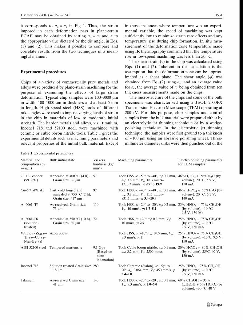
Table 1 Experimental parameters
Material andcomposition (byweight)
Bulk initial state Vickershardness (kg/mm2)
Machining parameters Electro-polishing parametersfor TEM samples
OFHC copper(99.98%)
Annealed at 400 �C (4 h),Grain size: 96 lm
57 Tool: HSS, a: +50� to –40�, ao: 0.1 mm,aw: 3.8 mm, Vo: 18.3 mm/s–1313.3 mm/s, c: 2.9 to 19.9
46%H3PO4 + 56%H2O (byvolume), 20 �C, 5.5 V,130 mA
Cu–6.7 at% Al Cast, cold forged andannealed at 750 �C (2 h),Grain size: 417 lm
97 Tool: HSS, a: +40� to –40�, ao: 0.1 mm,aw: 3.8 mm, Vo: 11.7 mm/s–831.7 mm/s, c: 3.4–10.9
46% H3PO4 + 56%H2O (byvolume), 20 �C, 6.1 V,140 mA
Al 6061–T6 As-received, Grain size:75 lm
110 Tool: HSS, a: +20� to –20�, ao: 0.2 mm,Vo: 10 mm/s, c: 1.7–5.2
25% HNO3 + 75% CH3OH(by volume), –10 �C,9.5 V, 150 Ma
Al 6061-T6(solution-treated)
Annealed at 550 �C (10 h),Grain size: 30 lm
72 Tool: HSS, a: +20� ao: 0.2 mm, Vo:10 mm/s, c: 2.7
25% HNO3 + 75% CH3OH(by volume), –10 �C,9.5 V, 150 mA
Vitreloy (Zr41.25–Ti13.75–Cu12.5–Ni10–Be22.5)
Amorphous Tool: HSS, a: +10�, ao: 0.05 mm, Vo:8.3 mm/s, c: 2
25% HNO3 + 75% CH3OH(by volume), –10�C, 9.5 V,150 mA
AISI 52100 steel Tempered martensite 9.1 Gpa(Based onnano-indenation)
Tool: Cubic boron nitride, ao: 0.1 mm,aw: 3.2 mm, Vo: 2500 mm/s
20% HClO4 + 80% CH3OH(by volume), 25�C, 40 V,130 mA
Inconel 718 Solution treated Grain size:18 lm
280 Tool: Ceramic (Sialon), a: +5(� to –20�, ao: 0.064 mm, Vo: 450 mm/s, c:2.4–7.8
25% HNO3 + 75% CH3OH(by volume), –10 �C,9.5 V, 150 mA
Titanium As-received Grain size:41 lm
143 Tool: HSS, a: +20� to –20�, ao: 0.1 mm,Vo: 8.3 mm/s, c: 2.0–6.0
60% CH3OH + 35%C4H9OH + 5% HClO4 (byvolume), –30 �C, 40 V
123
J Mater Sci (2007) 42:1529–1541 1531
ground samples and were made electron transparent by
electrolytic twin-jet thinning on a Struers Tenupol-5
polishing system. The electrolytes and conditions used
for preparing TEM specimens, from different materials,
by twin-jet thinning are given in Table 1. For the
wedge-polishing technique, the specimens were
mechanically thinned by abrasive polishing to form
shallow wedges. Each wedge was then mounted on a
copper slot grid and milled using Argon ions, at low
incident angles (<5�), for 5–10 min in a Gatan Model
600 dual ion mill to create an electron transparent
specimen. Care was taken to avoid any prolonged
heating of the specimens during the mechanical thin-
ning and ion milling in order to ensure the integrity of
the microstructure of the chip.
Bright- and dark-field images, along with selected
area diffraction patterns (SAD), were taken to analyze
grain size, defect structure and subgrain misorienta-
tion. The average grain size was determined by
sampling 50–100 grains using Heyn’s line intercept
method. If the aspect ratio, defined as the ratio of the
length to width of a grain, of the grains was greater
than 2, then the grain was considered as elongated;
otherwise the grain was taken to be equi-axed. For
those chips with elongated grain microstructures, the
mean width of a grain is reported as the grain size.
Some of the chip and bulk samples were polished for
microstructure analysis and hardness testing. Hardness
measurements were made using Vickers indentation
taking care to ensure that the size of an indentation, as
measured by its diagonal length, was kept about the
same in the bulk and chip samples so as to minimize
any uncertainties arising from an indentation ‘size
effect’. Furthermore, the size of a hardness indentation
was kept appropriately smaller than the specimen size
to eliminate edge effects. An average value for the
hardness was obtained by performing at least 15
indents in each sample.
Results
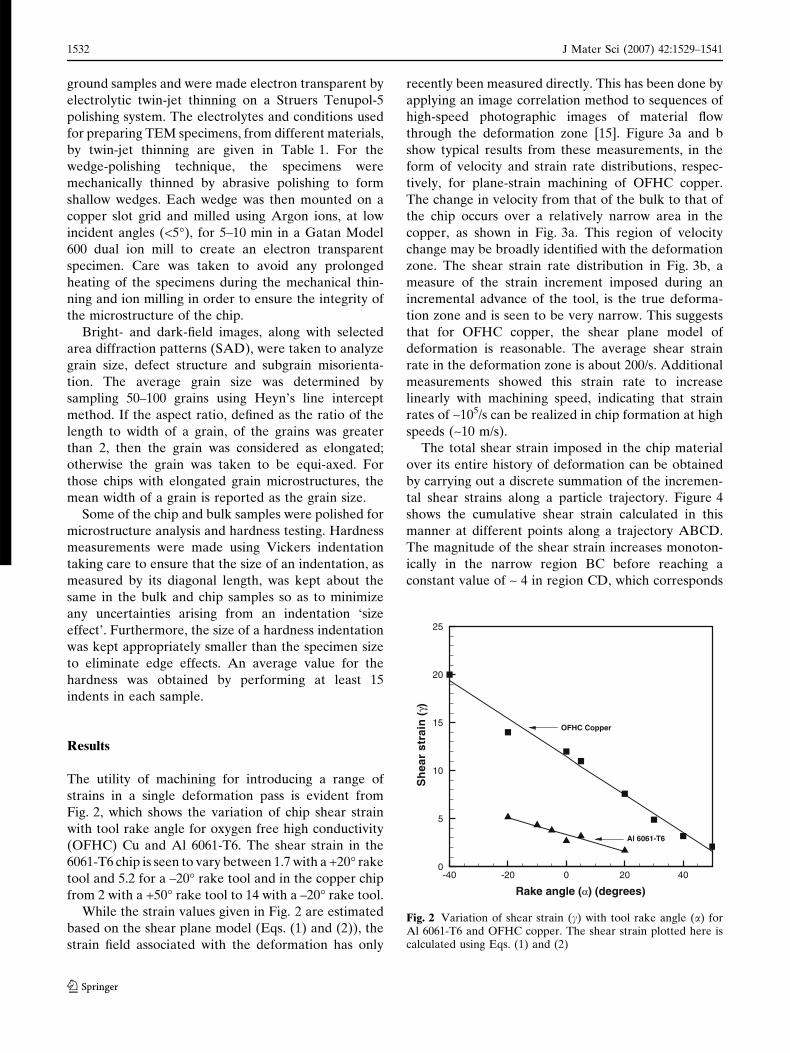
The utility of machining for introducing a range of
strains in a single deformation pass is evident from
Fig. 2, which shows the variation of chip shear strain
with tool rake angle for oxygen free high conductivity
(OFHC) Cu and Al 6061-T6. The shear strain in the
6061-T6 chip is seen to vary between 1.7 with a +20� rake
tool and 5.2 for a –20� rake tool and in the copper chip
from 2 with a +50� rake tool to 14 with a –20� rake tool.
While the strain values given in Fig. 2 are estimated
based on the shear plane model (Eqs. (1) and (2)), the
strain field associated with the deformation has only
recently been measured directly. This has been done by
applying an image correlation method to sequences of
high-speed photographic images of material flow
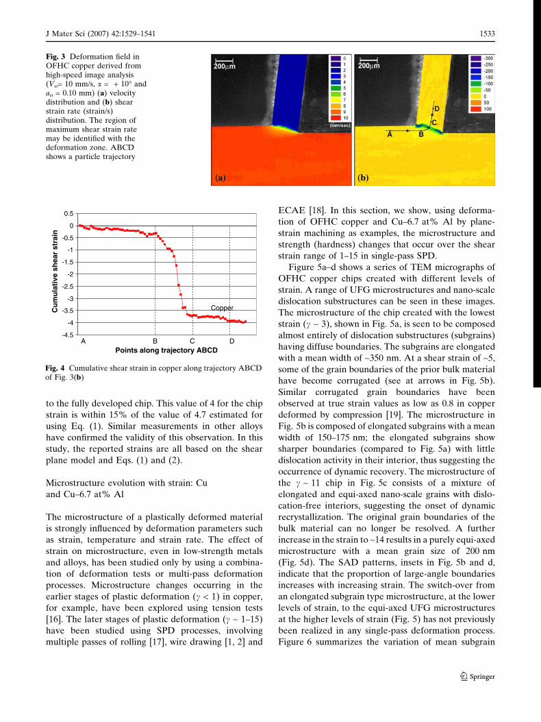
through the deformation zone [15]. Figure 3a and b
show typical results from these measurements, in the
form of velocity and strain rate distributions, respec-
tively, for plane-strain machining of OFHC copper.
The change in velocity from that of the bulk to that of
the chip occurs over a relatively narrow area in the
copper, as shown in Fig. 3a. This region of velocity
change may be broadly identified with the deformation
zone. The shear strain rate distribution in Fig. 3b, a
measure of the strain increment imposed during an
incremental advance of the tool, is the true deforma-
tion zone and is seen to be very narrow. This suggests
that for OFHC copper, the shear plane model of
deformation is reasonable. The average shear strain
rate in the deformation zone is about 200/s. Additional
measurements showed this strain rate to increase
linearly with machining speed, indicating that strain
rates of ~105/s can be realized in chip formation at high
speeds (~10 m/s).
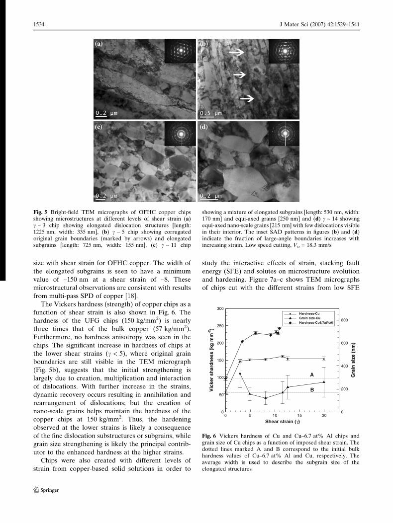
The total shear strain imposed in the chip material
over its entire history of deformation can be obtained
by carrying out a discrete summation of the incremen-
tal shear strains along a particle trajectory. Figure 4
shows the cumulative shear strain calculated in this
manner at different points along a trajectory ABCD.
The magnitude of the shear strain increases monoton-
ically in the narrow region BC before reaching a
constant value of ~ 4 in region CD, which corresponds
Rake angle (α) (degrees)
Sh
ear
stra
in (
γ)
-40 -20 0 20 400
5
10
15
20
25
OFHC Copper
Al 6061-T6
Fig. 2 Variation of shear strain (c) with tool rake angle (a) forAl 6061-T6 and OFHC copper. The shear strain plotted here iscalculated using Eqs. (1) and (2)
123
1532 J Mater Sci (2007) 42:1529–1541
to the fully developed chip. This value of 4 for the chip
strain is within 15% of the value of 4.7 estimated for
using Eq. (1). Similar measurements in other alloys
have confirmed the validity of this observation. In this
study, the reported strains are all based on the shear
plane model and Eqs. (1) and (2).
Microstructure evolution with strain: Cu
and Cu–6.7 at% Al
The microstructure of a plastically deformed material
is strongly influenced by deformation parameters such
as strain, temperature and strain rate. The effect of
strain on microstructure, even in low-strength metals
and alloys, has been studied only by using a combina-
tion of deformation tests or multi-pass deformation
processes. Microstructure changes occurring in the
earlier stages of plastic deformation (c < 1) in copper,
for example, have been explored using tension tests
[16]. The later stages of plastic deformation (c ~ 1–15)
have been studied using SPD processes, involving
multiple passes of rolling [17], wire drawing [1, 2] and
ECAE [18]. In this section, we show, using deforma-
tion of OFHC copper and Cu–6.7 at% Al by plane-
strain machining as examples, the microstructure and
strength (hardness) changes that occur over the shear
strain range of 1–15 in single-pass SPD.
Figure 5a–d shows a series of TEM micrographs of
OFHC copper chips created with different levels of
strain. A range of UFG microstructures and nano-scale
dislocation substructures can be seen in these images.
The microstructure of the chip created with the lowest
strain (c ~ 3), shown in Fig. 5a, is seen to be composed
almost entirely of dislocation substructures (subgrains)
having diffuse boundaries. The subgrains are elongated
with a mean width of ~350 nm. At a shear strain of ~5,
some of the grain boundaries of the prior bulk material
have become corrugated (see at arrows in Fig. 5b).
Similar corrugated grain boundaries have been
observed at true strain values as low as 0.8 in copper
deformed by compression [19]. The microstructure in
Fig. 5b is composed of elongated subgrains with a mean
width of 150–175 nm; the elongated subgrains show
sharper boundaries (compared to Fig. 5a) with little
dislocation activity in their interior, thus suggesting the
occurrence of dynamic recovery. The microstructure of
the c ~ 11 chip in Fig. 5c consists of a mixture of
elongated and equi-axed nano-scale grains with dislo-
cation-free interiors, suggesting the onset of dynamic
recrystallization. The original grain boundaries of the
bulk material can no longer be resolved. A further
increase in the strain to ~14 results in a purely equi-axed
microstructure with a mean grain size of 200 nm
(Fig. 5d). The SAD patterns, insets in Fig. 5b and d,
indicate that the proportion of large-angle boundaries
increases with increasing strain. The switch-over from
an elongated subgrain type microstructure, at the lower
levels of strain, to the equi-axed UFG microstructures
at the higher levels of strain (Fig. 5) has not previously
been realized in any single-pass deformation process.
Figure 6 summarizes the variation of mean subgrain
-4.5
-4
-3.5
-3
-2.5
-2
-1.5
-1
-0.5
0
0.5
Points along trajectory ABCD
Cu
mu
lati
ve s
hea
r st
rain
Copper
A B C D
Fig. 4 Cumulative shear strain in copper along trajectory ABCDof Fig. 3(b)
Fig. 3 Deformation field inOFHC copper derived fromhigh-speed image analysis(Vo= 10 mm/s, a = + 10� andao = 0.10 mm) (a) velocitydistribution and (b) shearstrain rate (strain/s)distribution. The region ofmaximum shear strain ratemay be identified with thedeformation zone. ABCDshows a particle trajectory
123
J Mater Sci (2007) 42:1529–1541 1533
size with shear strain for OFHC copper. The width of
the elongated subgrains is seen to have a minimum
value of ~150 nm at a shear strain of ~8. These
microstructural observations are consistent with results
from multi-pass SPD of copper [18].
The Vickers hardness (strength) of copper chips as a
function of shear strain is also shown in Fig. 6. The
hardness of the UFG chips (150 kg/mm2) is nearly
three times that of the bulk copper (57 kg/mm2).
Furthermore, no hardness anisotropy was seen in the
chips. The significant increase in hardness of chips at
the lower shear strains (c < 5), where original grain
boundaries are still visible in the TEM micrograph
(Fig. 5b), suggests that the initial strengthening is
largely due to creation, multiplication and interaction
of dislocations. With further increase in the strains,
dynamic recovery occurs resulting in annihilation and
rearrangement of dislocations; but the creation of
nano-scale grains helps maintain the hardness of the
copper chips at 150 kg/mm2. Thus, the hardening
observed at the lower strains is likely a consequence
of the fine dislocation substructures or subgrains, while
grain size strengthening is likely the principal contrib-
utor to the enhanced hardness at the higher strains.
Chips were also created with different levels of
strain from copper-based solid solutions in order to
study the interactive effects of strain, stacking fault
energy (SFE) and solutes on microstructure evolution
and hardening. Figure 7a–c shows TEM micrographs
of chips cut with the different strains from low SFE
Fig. 5 Bright-field TEM micrographs of OFHC copper chipsshowing microstructures at different levels of shear strain (a)c ~ 3 chip showing elongated dislocation structures [length:1225 nm, width: 335 nm], (b) c ~ 5 chip showing corrugatedoriginal grain boundaries (marked by arrows) and elongatedsubgrains [length: 725 nm, width: 155 nm], (c) c ~ 11 chip
showing a mixture of elongated subgrains [length: 530 nm, width:170 nm] and equi-axed grains [250 nm] and (d) c ~ 14 showingequi-axed nano-scale grains [215 nm] with few dislocations visiblein their interior. The inset SAD patterns in figures (b) and (d)indicate the fraction of large-angle boundaries increases withincreasing strain. Low speed cutting, Vo = 18.3 mm/s
Shear strain (γ)
Vic
ker
shar
dn
ess
(kg
mm
-2)
Gra
in s
ize
(nm
)
0 5 10 15 200
50
100
150
200
250
300
0
200
400
600
800
Hardness-CuGrain size-CuHardness-Cu6.7at%Al
A
B
Fig. 6 Vickers hardness of Cu and Cu–6.7 at% Al chips andgrain size of Cu chips as a function of imposed shear strain. Thedotted lines marked A and B correspond to the initial bulkhardness values of Cu–6.7 at% Al and Cu, respectively. Theaverage width is used to describe the subgrain size of theelongated structures
123
1534 J Mater Sci (2007) 42:1529–1541
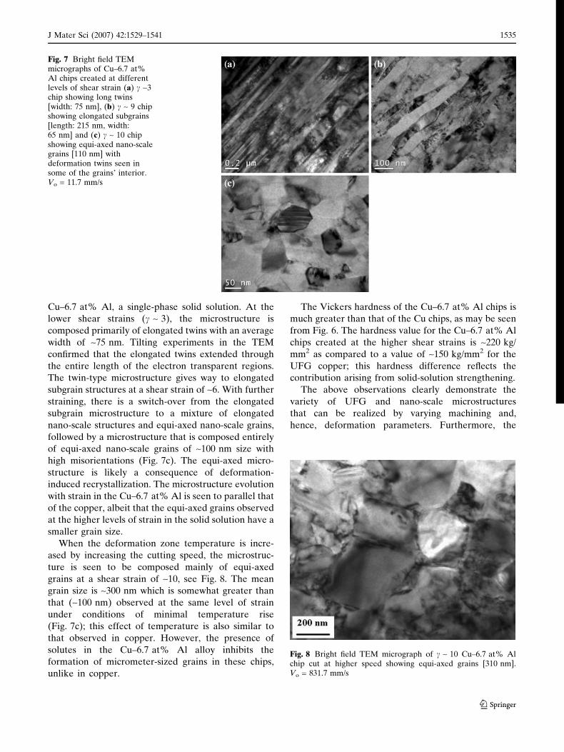
Cu–6.7 at% Al, a single-phase solid solution. At the
lower shear strains (c ~ 3), the microstructure is
composed primarily of elongated twins with an average
width of ~75 nm. Tilting experiments in the TEM
confirmed that the elongated twins extended through
the entire length of the electron transparent regions.
The twin-type microstructure gives way to elongated
subgrain structures at a shear strain of ~6. With further
straining, there is a switch-over from the elongated
subgrain microstructure to a mixture of elongated
nano-scale structures and equi-axed nano-scale grains,
followed by a microstructure that is composed entirely
of equi-axed nano-scale grains of ~100 nm size with
high misorientations (Fig. 7c). The equi-axed micro-
structure is likely a consequence of deformation-
induced recrystallization. The microstructure evolution
with strain in the Cu–6.7 at% Al is seen to parallel that
of the copper, albeit that the equi-axed grains observed
at the higher levels of strain in the solid solution have a
smaller grain size.
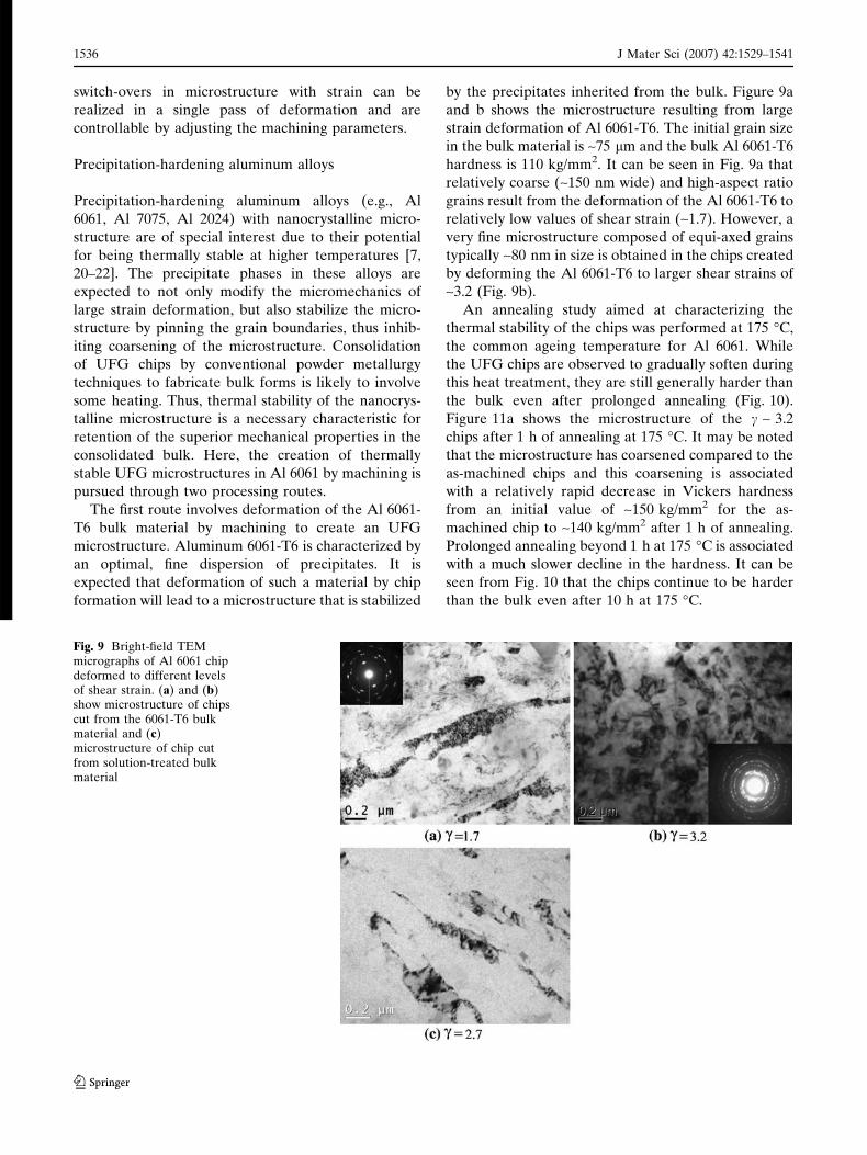
When the deformation zone temperature is incre-
ased by increasing the cutting speed, the microstruc-
ture is seen to be composed mainly of equi-axed
grains at a shear strain of ~10, see Fig. 8. The mean
grain size is ~300 nm which is somewhat greater than
that (~100 nm) observed at the same level of strain
under conditions of minimal temperature rise
(Fig. 7c); this effect of temperature is also similar to
that observed in copper. However, the presence of
solutes in the Cu–6.7 at% Al alloy inhibits the
formation of micrometer-sized grains in these chips,
unlike in copper.
The Vickers hardness of the Cu–6.7 at% Al chips is
much greater than that of the Cu chips, as may be seen
from Fig. 6. The hardness value for the Cu–6.7 at% Al
chips created at the higher shear strains is ~220 kg/
mm2 as compared to a value of ~150 kg/mm2 for the
UFG copper; this hardness difference reflects the
contribution arising from solid-solution strengthening.
The above observations clearly demonstrate the
variety of UFG and nano-scale microstructures
that can be realized by varying machining and,
hence, deformation parameters. Furthermore, the
Fig. 7 Bright field TEMmicrographs of Cu–6.7 at%Al chips created at differentlevels of shear strain (a) c ~3chip showing long twins[width: 75 nm], (b) c ~ 9 chipshowing elongated subgrains[length: 215 nm, width:65 nm] and (c) c ~ 10 chipshowing equi-axed nano-scalegrains [110 nm] withdeformation twins seen insome of the grains’ interior.Vo = 11.7 mm/s
Fig. 8 Bright field TEM micrograph of c ~ 10 Cu–6.7 at% Alchip cut at higher speed showing equi-axed grains [310 nm].Vo = 831.7 mm/s
123
J Mater Sci (2007) 42:1529–1541 1535
switch-overs in microstructure with strain can be
realized in a single pass of deformation and are
controllable by adjusting the machining parameters.
Precipitation-hardening aluminum alloys
Precipitation-hardening aluminum alloys (e.g., Al
6061, Al 7075, Al 2024) with nanocrystalline micro-
structure are of special interest due to their potential
for being thermally stable at higher temperatures [7,
20–22]. The precipitate phases in these alloys are
expected to not only modify the micromechanics of
large strain deformation, but also stabilize the micro-
structure by pinning the grain boundaries, thus inhib-
iting coarsening of the microstructure. Consolidation
of UFG chips by conventional powder metallurgy
techniques to fabricate bulk forms is likely to involve
some heating. Thus, thermal stability of the nanocrys-
talline microstructure is a necessary characteristic for
retention of the superior mechanical properties in the
consolidated bulk. Here, the creation of thermally
stable UFG microstructures in Al 6061 by machining is
pursued through two processing routes.
The first route involves deformation of the Al 6061-
T6 bulk material by machining to create an UFG
microstructure. Aluminum 6061-T6 is characterized by
an optimal, fine dispersion of precipitates. It is
expected that deformation of such a material by chip
formation will lead to a microstructure that is stabilized
by the precipitates inherited from the bulk. Figure 9a
and b shows the microstructure resulting from large
strain deformation of Al 6061-T6. The initial grain size
in the bulk material is ~75 lm and the bulk Al 6061-T6
hardness is 110 kg/mm2. It can be seen in Fig. 9a that
relatively coarse (~150 nm wide) and high-aspect ratio
grains result from the deformation of the Al 6061-T6 to
relatively low values of shear strain (~1.7). However, a
very fine microstructure composed of equi-axed grains
typically ~80 nm in size is obtained in the chips created
by deforming the Al 6061-T6 to larger shear strains of
~3.2 (Fig. 9b).
An annealing study aimed at characterizing the
thermal stability of the chips was performed at 175 �C,
the common ageing temperature for Al 6061. While
the UFG chips are observed to gradually soften during
this heat treatment, they are still generally harder than
the bulk even after prolonged annealing (Fig. 10).
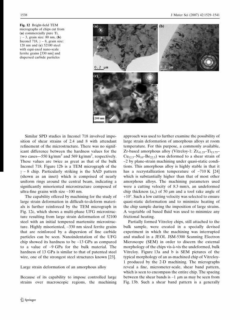
Figure 11a shows the microstructure of the c ~ 3.2
chips after 1 h of annealing at 175 �C. It may be noted
that the microstructure has coarsened compared to the
as-machined chips and this coarsening is associated
with a relatively rapid decrease in Vickers hardness
from an initial value of ~150 kg/mm2 for the as-
machined chip to ~140 kg/mm2 after 1 h of annealing.
Prolonged annealing beyond 1 h at 175 �C is associated
with a much slower decline in the hardness. It can be
seen from Fig. 10 that the chips continue to be harder
than the bulk even after 10 h at 175 �C.
Fig. 9 Bright-field TEMmicrographs of Al 6061 chipdeformed to different levelsof shear strain. (a) and (b)show microstructure of chipscut from the 6061-T6 bulkmaterial and (c)microstructure of chip cutfrom solution-treated bulkmaterial
123
1536 J Mater Sci (2007) 42:1529–1541
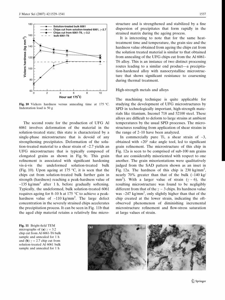
The second route for the production of UFG Al
6061 involves deformation of the material in the
solution-treated state; this state is characterized by a
single-phase microstructure that is devoid of any
strengthening precipitates. Deformation of the solu-
tion-treated material to a shear strain of ~2.7 yields an
UFG microstructure that is typically composed of
elongated grains as shown in Fig. 9c. This grain
refinement is associated with significant hardening
vis-a-vis the undeformed solution-treated bulk
(Fig. 10). Upon ageing at 175 �C, it is seen that the
chips cut from solution-treated bulk further gain in
strength (hardness) reaching a peak-hardness value of
~135 kg/mm2 after 1 h, before gradually softening.
Typically, the undeformed, bulk solution-treated 6061
requires ageing for 8–10 h at 175 �C to achieve a peak-
hardness value of ~110 kg/mm2. The large defect
concentration in the severely strained chips accelerates
the precipitation process. It can be seen in Fig. 11b that
the aged chip material retains a relatively fine micro-
structure and is strengthened and stabilized by a fine
dispersion of precipitates that form rapidly in the
strained matrix during the ageing process.
It is interesting to note that for the same heat-
treatment time and temperature, the grain size and the
hardness value obtained from ageing the chips cut from
the solution treated material is similar to that obtained
from annealing of the UFG chips cut from the Al 6061-
T6 alloy. This is an instance of two distinct processing
routes leading to a similar end product—a precipita-
tion-hardened alloy with nanocrystalline microstruc-
ture that shows significant resistance to coarsening
during thermal treatment.
High-strength metals and alloys
The machining technique is quite applicable for
studying the development of UFG microstructures by
SPD in technologically important, high-strength mate-
rials like titanium, Inconel 718 and 52100 steel. These
alloys are difficult to deform to large strains at ambient
temperatures by the usual SPD processes. The micro-
structures resulting from application of shear strains in
the range of 2–10 have been analyzed.
In commercially pure Ti, a shear strain of ~3,
obtained with +20� rake angle tool, led to significant
grain refinement. The microstructure of this chip in
Fig. 12a is seen to be comprised of sub-100 nm grains
that are considerably misoriented with respect to one
another. The grain misorientations were qualitatively
judged from the SAD pattern shown as an inset in
Fig. 12a. The hardness of this chip is 230 kg/mm2,
nearly 70% greater than that of the bulk (~140 kg/
mm2). With a larger value of strain (c ~ 6), the
resulting microstructure was found to be negligibly
different from that of the c ~ 3 chips. Its hardness value
was ~247 kg/mm2, only slightly higher than that of the
chip created at the lower strain, indicating the oft-
observed phenomenon of diminishing incremental
microstructure refinement and flow-stress saturation
at large values of strain.
Hour sat 175oC
Vic
kers
har
dn
ess
(kg
mm
-2)
0 8 1060
80
100
120
140
160
180Solution-treated bulk 6061Chips cut from solution-treated 6061, γ~2.7Chips cut from 6061-T6, γ~3.2bulk 6061-T6
2 4 6
Fig. 10 Vickers hardness versus annealing time at 175 �C.Indentation load is 50 g
Fig. 11 Bright-field TEMmicrographs of (a) c = 3.2chip cut from Al 6061-T6 bulksample and annealed for 1 hand (b) c = 2.7 chip cut fromsolution-treated Al 6061 bulksample and annealed for 1 h
123
J Mater Sci (2007) 42:1529–1541 1537
Similar SPD studies in Inconel 718 involved impo-
sition of shear strains of 2.4 and 8 with attendant
refinement of the microstructure. There was no signif-
icant difference between the hardness values for the
two cases—550 kg/mm2 and 569 kg/mm2, respectively.
These values are twice as great as that of the bulk
Inconel 718. Figure 12b is a TEM micrograph of the
c ~ 8 chip. Particularly striking is the SAD pattern
(shown as an inset) which is comprised of nearly
uniform rings around the central beam, indicating a
significantly misoriented microstructure composed of
ultra-fine grains with size ~100 nm.
The capability offered by machining for the study of
large strain deformation in difficult-to-deform materi-
als is further reinforced by the TEM micrograph in
Fig. 12c, which shows a multi-phase UFG microstruc-
ture resulting from large strain deformation of 52100
steel with an initial tempered martensite microstruc-
ture. Highly misoriented, ~330 nm sized ferrite grains
that are reinforced by a dispersion of fine carbide
particles can be seen. Nanoindentation of the UFG
chip showed its hardness to be ~13 GPa as compared
to a value of ~9 GPa for the bulk material. The
hardness of 13 GPa is similar to that of patented steel
wire, one of the strongest steel structures known [23].
Large strain deformation of an amorphous alloy
Because of its capability to impose controlled large
strains over macroscopic regions, the machining
approach was used to further examine the possibility of
large strain deformation of amorphous alloys at room
temperature. For this purpose, a commonly available,
Zr-based amorphous alloy (Vitreloy-1: Zr41.25–Ti13.75–
Cu12.5–Ni10–Be22.5) was deformed to a shear strain of
~2 by plane-strain machining under quasi-static condi-
tions. This amorphous alloy is highly stable in that it
has a recrystallization temperature of ~710 K [24]
which is substantially higher than that of most other
amorphous alloys. The machining parameters used
were a cutting velocity of 8.3 mm/s, an undeformed
chip thickness (ao) of 50 lm and a tool rake angle of
+10�. Such a low cutting velocity was selected to ensure
quasi-static deformation and to minimize heating of
the chip sample during the imposition of large strains.
A vegetable oil based fluid was used to minimize any
frictional heating.
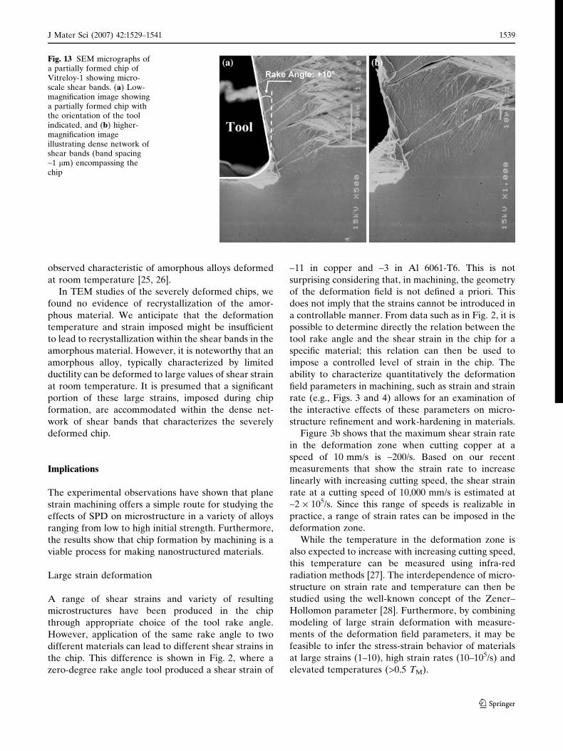
Partially formed Vitreloy chips, still attached to the
bulk sample, were created in a specially devised
experiment in which the machining was interrupted
and studied in a JEOL JSM-5300 Scanning Electron
Microscope (SEM) in order to discern the external
morphology of the chips vis-a-vis the undeformed, bulk
Vitreloy. Figure 13a and b is SEM pictures of the
typical morphology of an as-machined chip of Vitreloy-
1 produced by the 2-D machining. The micrographs
reveal a fine, micrometer-scale, shear band pattern,
which is seen to encompass the entire chip. The spacing
between the shear bands is ~1 lm as may be seen from
Fig. 13b. Such a shear band pattern is a generally
Fig. 12 Bright-field TEMmicrographs of chips cut from(a) commercially pure Ti,c ~ 3, grain size: 80 nm, (b)Inconel 718, c ~ 8, grain size:120 nm and (c) 52100 steelwith equi-axed nano-scaleferrite grains [330 nm] anddispersed carbide particles
123
1538 J Mater Sci (2007) 42:1529–1541
observed characteristic of amorphous alloys deformed
at room temperature [25, 26].
In TEM studies of the severely deformed chips, we
found no evidence of recrystallization of the amor-
phous material. We anticipate that the deformation
temperature and strain imposed might be insufficient
to lead to recrystallization within the shear bands in the
amorphous material. However, it is noteworthy that an
amorphous alloy, typically characterized by limited
ductility can be deformed to large values of shear strain
at room temperature. It is presumed that a significant
portion of these large strains, imposed during chip
formation, are accommodated within the dense net-
work of shear bands that characterizes the severely
deformed chip.
Implications
The experimental observations have shown that plane
strain machining offers a simple route for studying the
effects of SPD on microstructure in a variety of alloys
ranging from low to high initial strength. Furthermore,
the results show that chip formation by machining is a
viable process for making nanostructured materials.
Large strain deformation
A range of shear strains and variety of resulting
microstructures have been produced in the chip
through appropriate choice of the tool rake angle.
However, application of the same rake angle to two
different materials can lead to different shear strains in
the chip. This difference is shown in Fig. 2, where a
zero-degree rake angle tool produced a shear strain of
~11 in copper and ~3 in Al 6061-T6. This is not
surprising considering that, in machining, the geometry
of the deformation field is not defined a priori. This
does not imply that the strains cannot be introduced in
a controllable manner. From data such as in Fig. 2, it is
possible to determine directly the relation between the
tool rake angle and the shear strain in the chip for a
specific material; this relation can then be used to
impose a controlled level of strain in the chip. The
ability to characterize quantitatively the deformation
field parameters in machining, such as strain and strain
rate (e.g., Figs. 3 and 4) allows for an examination of
the interactive effects of these parameters on micro-
structure refinement and work-hardening in materials.
Figure 3b shows that the maximum shear strain rate
in the deformation zone when cutting copper at a
speed of 10 mm/s is ~200/s. Based on our recent
measurements that show the strain rate to increase
linearly with increasing cutting speed, the shear strain
rate at a cutting speed of 10,000 mm/s is estimated at
~2 · 105/s. Since this range of speeds is realizable in
practice, a range of strain rates can be imposed in the
deformation zone.
While the temperature in the deformation zone is
also expected to increase with increasing cutting speed,
this temperature can be measured using infra-red
radiation methods [27]. The interdependence of micro-
structure on strain rate and temperature can then be
studied using the well-known concept of the Zener–
Hollomon parameter [28]. Furthermore, by combining
modeling of large strain deformation with measure-
ments of the deformation field parameters, it may be
feasible to infer the stress-strain behavior of materials
at large strains (1–10), high strain rates (10–105/s) and
elevated temperatures (>0.5 TM).
Fig. 13 SEM micrographs ofa partially formed chip ofVitreloy-1 showing micro-scale shear bands. (a) Low-magnification image showinga partially formed chip withthe orientation of the toolindicated, and (b) higher-magnification imageillustrating dense network ofshear bands (band spacing~1 lm) encompassing thechip
123
J Mater Sci (2007) 42:1529–1541 1539
Microstructure development
The ability to control the microstructure by varying the
deformation conditions in machining has been demon-
strated. The minimum grain sizes that have been
realized to date in SPD by machining range from
~60 nm in precipitation hardening alloys such as Al
6061-T6 to ~160 nm in pure metals such as copper
(Fig. 5). This scale of the microstructure in Al 6061-T6
is somewhat finer than that observed in the same alloy
processed by warm ECAE [20]. The addition of small
amounts of solute to pure metals is seen to result in
smaller grain sizes; for example, the smallest grain size
created by the machining in Cu–6.7 at% Al is ~100 nm.
Similar observations have been made in other solid
solutions of copper. Additional evidence in support of
finer-scale microstructures in alloys can be found in
observations of ~100 nm sized grains in Inconel 718
created by machining (Fig. 12). This is likely a conse-
quence of the deformation-induced microstructure
being stabilized by the solutes and precipitates.
A switch-over has been observed from an elongated
UFG microstructure at lower strains to an equi-axed
nanocrystalline microstructure, with relatively low
density of dislocations, at the higher strains (Figs. 5
and 7). The equi-axed microstructure is likely a
consequence of dynamic recrystallization occurring
during machining.
The nanostructured chip materials are up to three
times harder than the corresponding bulk material in
the micro-crystalline form (e.g., Fig. 6). The hardness
values of the Cu and Cu–6.7 at% Al chips increase
quite steeply with imposed strain, initially, but change
negligibly at the higher strains. This is true also for the
Al 6061 alloys [29]. The hardness saturation at the
relatively low strains occurs even though the micro-
structure often evolves from an elongated subgrain
type structure at the lower strains to an equi-axed fine
grained microstructure, with high degree of misorien-
tations, at the higher strains. This suggests that the
microstructure contribution to the strengthening is
different at the lower (dislocation substructure
strengthening) and higher strains (grain size strength-
ening). While we have not yet measured the ductility
corresponding to these two types of microstructures, it
is likely that they are different. The equi-axed micro-
structures are likely to show a greater ductility than the
elongated subgrain type microstructures. Tensile tests
on the chip samples should provide the answer to this
question of microstructure dependence of ductility.
Chip samples several millimeters wide and up to
several hundred micrometers thick are easy to create by
machining. Miniature tensile specimens can be fash-
ioned out of these ‘‘bulk’’ chip samples and used to
directly assess intrinsic mechanical properties such as
yield stress, ductility, fatigue strength and fracture
toughness. Preliminary measurements of the yield
strength of an OFHC copper chip sample made in this
manner have shown that the enhancement in the
strength of the chip relative to the bulk sample is similar
to that of the measured increase in the Vickers hardness.
The chip samples can also be used to characterize
thermal stability of the nanocrystalline and UFG
microstructures, as has been done with Al 6061.
Production of nanostructured materials
The experiments have provided clear evidence that
nanocrystalline metals and alloys of high strength are
formed through a normal machining process. Perhaps
more important, this process provides an avenue for
the production of nanocrystalline structures in a far
wider range of materials and at far lower costs than has
been foreseen using other processes. An UFG struc-
ture of virtually any metal or alloy can be produced
through the same basic process.
Machining is not normally considered a bulk defor-
mation process but, in principle, the size of chips is
limited only by machine power. Indeed, chips several
millimeters in thickness can be produced from initially
low strength alloys using commonly available machine
tools. Hence, machining reasonably can be considered
among the other bulk SPD processes. The process can
be scaled down, as well, giving it wide flexibility, by
simply changing cutting parameters.
The availability of large volumes of metal chips,
either as byproducts from existing manufacturing oper-
ations or from specific chip making processes, offer
opportunities to create structural materials with
mechanical properties that are influenced by the UFG
microstructure of the chips. Various comminution and
consolidation processes for converting chips to bulk
monolithic and composite components are the subject of
on-going research. An important consideration, as in
consolidating any nanostructured material, is to limit
heating in order to suppress coarsening phenomena.
While none of these processes have been fully developed
with these starting materials, preliminary results suggest
that the opportunity exists to create advanced materials
with new and interesting combinations of properties.
Conclusions
The study has established that controlled shear strains
in the range of 1–15 can be imposed in the chip in a
123
1540 J Mater Sci (2007) 42:1529–1541
single pass of plane-strain machining and the micro-
structure of the chip is substantially finer than that of
the bulk material. Furthermore, the deformation
parameters associated with chip formation including
strain and strain rate can be related to the machining
parameters such as tool rake angle and undeformed
chip thickness by direct measurement. Thus, machining
provides an experimental framework for studying
microstructure refinement by SPD in metals and alloys.
A microstructure composed of equi-axed sub-
100 nm grains, with a high degree of grain misorien-
tation, has been demonstrated in various alloys ranging
from low to high strength by appropriate selection of
the machining parameters. UFG microstructures, both
equi-axed and of the elongated subgrain type, have
been shown to occur in pure metals and select alloy
systems. The hardness (strength) of the UFG and
nanocrystalline materials created by machining is
significantly greater than that of the corresponding
microcrystalline forms.
Chip formation by machining provides an avenue
for the production of UFG microstructures in a far
wider group of materials and, potentially, at far lower
costs than has been foreseen using other processes.
Acknowledgements We would like to thank the Department ofEnergy (grant 4000031768 via UT-Batelle), Oak Ridge NationalLaboratory (ORNL), Ford Motor Company, the State ofIndiana’s 21st Century Research and Technology Fund, theNSF (Grants DMI 0500216 and CMS 0200509) and the USAF–PEWG program (via Anteon Corporation) for supporting thiswork. Additional thanks are also due Drs. Andrew Sherman(Ford) and Ray Johnson (ORNL) for their encouragement of thestudies. SS would like to acknowledge support of a NationalResearch Council Fellowship.
References
1. Embury JD, Fisher RM (1966) Acta Metall 14:1472. Langford G, Cohen M (1969) Trans ASM 62:6233. Segal VM, Reznikov VI, Drobyshevskiy AE, Kopylov V
(1981) Russ Metall 1:99
4. Valiev RZ, Islamgaliev RK, Alexandrov IV (2000) ProgMater Sci 45:103
5. Humphreys FJ, Prangnell PB, Bowen JR, Gholinia A, HarrisC (1999) Phil Trans R Soc Lond A357:1663
6. Hughes DA, Hansen N (2000) Acta Mater 48(11):29857. Horita Z, Fujinami T, Nemoto M, Langdon TG (2000)
Metall Mater Trans A31:6918. Brown TL, Swaminathan S, Chandrasekar S, Compton WD,
King AH, Trumble KP (2002) J Mater Res 17(10):24849. Swaminathan S, Ravi Shankar M, Lee S, Hwang J, King AH,
Kezar RF, Rao BC, Brown TL, Chandrasekar S, ComptonWD, Trumble KP (2005) Mater Sci Eng A 410–411:358
10. Ravi Shankar M, Rao BC, Lee S, Chandrasekar S , King AH,Compton WD (2006) Acta Mater 54:3691
11. Merchant ME (1945) J Appl Phys 16:26712. Shaw MC (1984) Metal cutting principles. Oxford University
Press13. Madhavan V, Chandrasekar S, Farris TN (2000) J Appl
Mech 67(1):12814. Moscoso W, Olgun E, Compton WD, Chandrasekar S (2005)
J Trib 127:23815. Lee S, Hwang J, Ravi Shankar M, Chandrasekar S, Compton
WD (2006) Metall Mater Trans A37:163316. Steeds JW (1966) Proc Royal Soc London A292:34317. Hirsch J, Lucke K, Hatherly M (1988) Acta Metall 36:290518. Dalla Torre F, Lapovok R, Sandlin J, Thomson PF, Davies
CHJ, Pereloma EV (2004) Acta Mater 52:481919. Belyakov A, Sakai T, Miura H, Tsuzaki K (2001) Phil Mag
81:262920. Ferrasse S, Segal VM, Hartwig KT, Goforth RE (1997) J
Mater Res 12:125321. Zhao YH, Liao XZ, Jin Z, Valiev RZ, Zhu YT (2004) Acta
Mater 52:458922. Kim WJ, Chung CS, Ma DS, Hong SI, Kim HK (2003)
Scripta Mater 49:33323. Kelly A, MacMillan NH (1986) Strong solids. Clarendon,
Oxford, UK, 222 pp and 373 pp24. Lu J, Ravichandran G, Johnson WL (2003) Acta Mater
51:342925. Kim JJ, Choi Y, Suresh S, Argon AS (2002) Science 295:65426. Chen H, He Y, Shiflet GJ, Poon SJ (1994) Nature 367:54127. Hwang J, Kompella S, Chandrasekar S, Farris TN (2003)
ASME J Tribol 125(2):37728. Humphreys FJ, Hatherly M (1996) Recrystallization and
related annealing phenomena. Pergamon, 364 pp and 391 pp29. Ravi Shankar M, Chandrasekar S, King AH, Compton WD
(2005) Mater Sci Eng A 410–411:365
123
J Mater Sci (2007) 42:1529–1541 1541


![Author's personal copy · 2012. 10. 16. · Severe plastic deformation (SPD) is an ef cient method for producing ultra- ne grain (UFG) materials [1]. Various SPD tech-niques like](https://img.pdfslide.us/doc/110x75/60b16c4745e33909671bdb87/authors-personal-2012-10-16-severe-plastic-deformation-spd-is-an-ef-cient.jpg)

![DIRECT AND REVERSE MARTENSITIC TRANSFORMATION AND ... · deformation (SPD) of metastable austenitic steels we observe direct ( o) and ( ) martensitic transformations (MTs) [1-3]](https://img.pdfslide.us/doc/110x75/5fedd562ca3da635561e7efc/direct-and-reverse-martensitic-transformation-and-deformation-spd-of-metastable.jpg)