Embed Size (px)
Citation preview
IEEE TRANSACTIONS ON NUCLEAR SCIENCE, VOL. 56, NO. 4, AUGUST 2009 2021
SET Emulation Considering ElectricalMasking Effects
Luis Entrena, Mario García Valderas, Raúl Fernández Cardenal, Marta Portela García, and Celia López Ongil
Abstract—A new approach is proposed for evaluating circuit ro-bustness against Single Event Transients (SETs) through FPGAemulation. A voltage-time quantization model allows capturing cir-cuit delays in the FPGA, including electrical masking effects. Ex-perimental results demonstrate this approach improves SET faultinjection rate by three orders of magnitude with respect to logicsimulation and provides an accuracy close to analog simulation.
Index Terms—Electrical masking, fault injection, FPGA emula-tion, single event transient (SET).
I. INTRODUCTION
A Single Event Transient (SET) results when a particlestrikes a sensitive node within combinational logic. It
produces a current pulse which becomes a voltage disturbancethat may propagate through the logic and finally be latchedby a sequential element, resulting in a soft error [1], [2]. Inthe past, the study of SET effects has received less attention,as the contribution of SETs to the Soft Error Rate (SER) hasbeen considered minor compared to the contributions of SingleEvent Upsets (SEU) on memory elements. However, as thetransistor feature size scales down, SET effects are becomingmore relevant. It has been predicted that in the near future, theSER due to combinational logic may be comparable to that ofthe memory elements [3].
In order to evaluate soft error rates due to SETs, fast and accu-rate analysis techniques of transient pulse propagation in com-binational logic are needed. There are three masking effects thatcan prevent a transient pulse in combinational logic from propa-gating and being latched by a memory element: logic masking,latch window masking, and electrical masking [3], [4]. Logicmasking occurs when the SET is not located in a sensitized pathand thus cannot be propagated to a sequential element. Latchwindow masking occurs when the transient reaches the sequen-tial elements outside of their latching time window. Electricalmasking occurs when the transient is attenuated by subsequentlogic gates until it is eventually filtered. These three maskingeffects are relevant to estimate the Soft Error Rate (SER). For
Manuscript received September 05, 2008; revised December 31, 2008. Cur-rent version published August 12, 2009. This work was supported in part by theRENASER Project (Ref.: ESP2007-65914-C03-01) funded by the Ministry ofEducation and Science of Spain.
The authors are with the Electronic Technology Department, Uni-versity Carlos III of Madrid, 28911 Leganes, Madrid, Spain (e-mail:[email protected]; [email protected]; [email protected];[email protected]; [email protected]).
Color versions of one or more of the figures in this paper are available onlineat http://ieeexplore.ieee.org.
Digital Object Identifier 10.1109/TNS.2009.2013346
instance, ignoring electrical masking effect can overestimate theSER by 138% for a small circuit, according to [5].
The first two masking effects can be analyzed with alogic-level simulator. Moreover, the analysis can be acceleratedby emulating a time-domain model of the Circuit Under Test(CUT) in a FPGA [7], [8]. In [7], a delay quantization model isproposed that enables emulation accelerating SET analysis bythree orders of magnitude with respect to logic-level simulation.However, electrical masking effects are not covered by theseapproaches, since it requires an electrical model of the CUT.Analyzing transient pulse propagation in combinational logiccircuits considering electrical masking effects in an efficientand accurate manner remains a significant challenge [4], [5] .
Electrical masking effects are a consequence of delay degra-dation as a transient is propagated through combinational logicgates. If the duration of the transient does not allow for a fullswing on the gate’s output, then a shorter transient is propa-gated. The transient may not be propagated at all if its dura-tion is smaller than the gate delay. Thus, evaluation of elec-trical masking effects requires a dynamic delay model that de-pends on input transient durations. Analytical estimations basedon approximated models can lead to large errors in transienterror analysis [10]. Although the models are being refined [5],[6], the run-time for SER estimation on typical combinationalbenchmark circuits ranges from 10 minutes to several hours [6].On the other hand, accurate estimations using analog simulators(e.g., SPICE) are not affordable except for very small circuits.
In this paper, a new approach for emulation-based SET anal-ysis that includes electrical masking effects is proposed. As in[7], this approach is based on quantization in order to capturethe time-domain behaviour of the Circuit Under Test in a FPGA.However, voltage quantization is used instead of delay quantiza-tion. Thus, partial voltage swings that may occur for short tran-sients and produce delay degradation can be properly modelled.This model can be easily captured in a FPGA with acceptableresource overhead. The proposed approach can be automated toincrease dramatically the performance of the SET fault analysisprocess with electrical-level accuracy.
The paper is organized as follows. In Section II, thevoltage-time quantization delay model is described. InSection III, this model is validated against electrical levelsimulations. In Section IV, the model is applied to severalbenchmark circuits and results are presented. Finally, Section Vshows the conclusions of this work.
II. DELAY MODEL AND VOLTAGE-TIME QUANTIZATION
The main problem that prevents FPGA-based emulation ofSETs is the capture of CUT delays into the FPGA. Synthesizing
0018-9499/$26.00 © 2009 IEEE
2022 IEEE TRANSACTIONS ON NUCLEAR SCIENCE, VOL. 56, NO. 4, AUGUST 2009
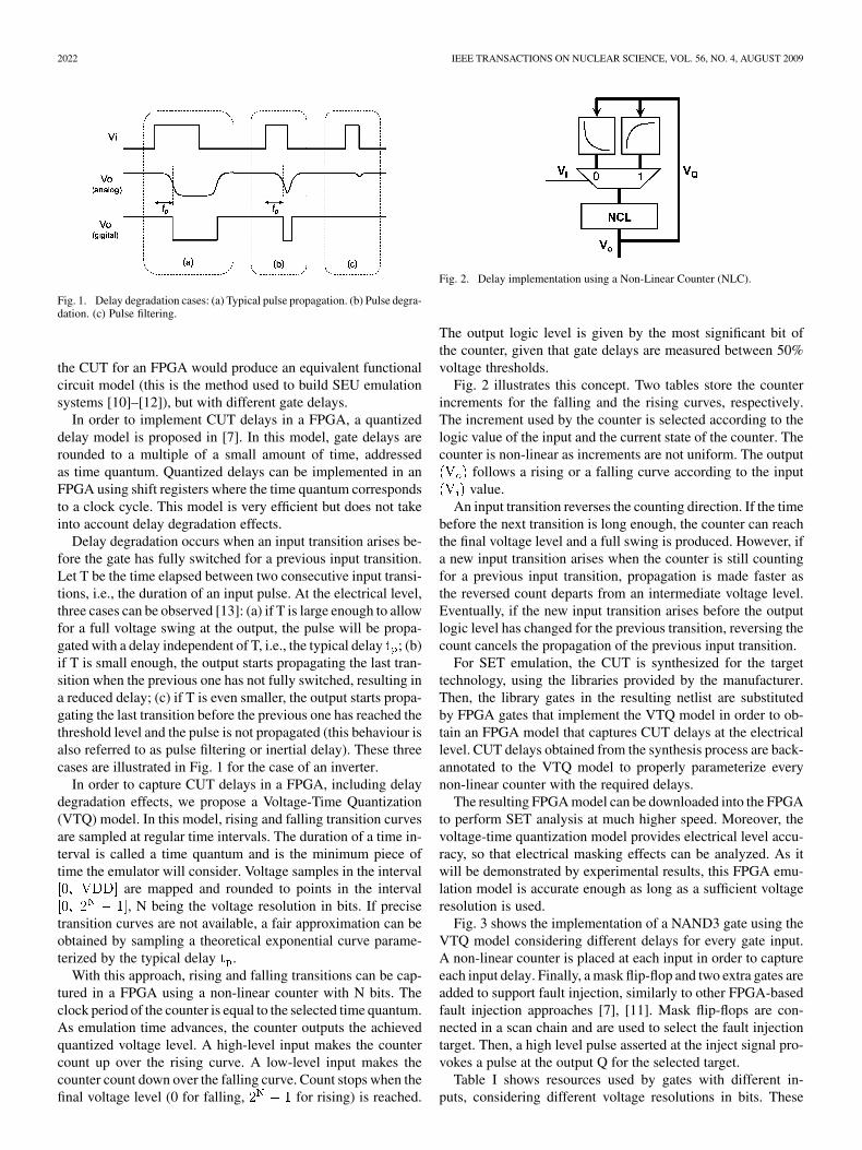
Fig. 1. Delay degradation cases: (a) Typical pulse propagation. (b) Pulse degra-dation. (c) Pulse filtering.
the CUT for an FPGA would produce an equivalent functionalcircuit model (this is the method used to build SEU emulationsystems [10]–[12]), but with different gate delays.
In order to implement CUT delays in a FPGA, a quantizeddelay model is proposed in [7]. In this model, gate delays arerounded to a multiple of a small amount of time, addressedas time quantum. Quantized delays can be implemented in anFPGA using shift registers where the time quantum correspondsto a clock cycle. This model is very efficient but does not takeinto account delay degradation effects.
Delay degradation occurs when an input transition arises be-fore the gate has fully switched for a previous input transition.Let T be the time elapsed between two consecutive input transi-tions, i.e., the duration of an input pulse. At the electrical level,three cases can be observed [13]: (a) if T is large enough to allowfor a full voltage swing at the output, the pulse will be propa-gated with a delay independent of T, i.e., the typical delay ; (b)if T is small enough, the output starts propagating the last tran-sition when the previous one has not fully switched, resulting ina reduced delay; (c) if T is even smaller, the output starts propa-gating the last transition before the previous one has reached thethreshold level and the pulse is not propagated (this behaviour isalso referred to as pulse filtering or inertial delay). These threecases are illustrated in Fig. 1 for the case of an inverter.
In order to capture CUT delays in a FPGA, including delaydegradation effects, we propose a Voltage-Time Quantization(VTQ) model. In this model, rising and falling transition curvesare sampled at regular time intervals. The duration of a time in-terval is called a time quantum and is the minimum piece oftime the emulator will consider. Voltage samples in the interval
are mapped and rounded to points in the interval, N being the voltage resolution in bits. If precise
transition curves are not available, a fair approximation can beobtained by sampling a theoretical exponential curve parame-terized by the typical delay .
With this approach, rising and falling transitions can be cap-tured in a FPGA using a non-linear counter with N bits. Theclock period of the counter is equal to the selected time quantum.As emulation time advances, the counter outputs the achievedquantized voltage level. A high-level input makes the countercount up over the rising curve. A low-level input makes thecounter count down over the falling curve. Count stops when thefinal voltage level (0 for falling, for rising) is reached.
Fig. 2. Delay implementation using a Non-Linear Counter (NLC).
The output logic level is given by the most significant bit ofthe counter, given that gate delays are measured between 50%voltage thresholds.
Fig. 2 illustrates this concept. Two tables store the counterincrements for the falling and the rising curves, respectively.The increment used by the counter is selected according to thelogic value of the input and the current state of the counter. Thecounter is non-linear as increments are not uniform. The output
follows a rising or a falling curve according to the inputvalue.
An input transition reverses the counting direction. If the timebefore the next transition is long enough, the counter can reachthe final voltage level and a full swing is produced. However, ifa new input transition arises when the counter is still countingfor a previous input transition, propagation is made faster asthe reversed count departs from an intermediate voltage level.Eventually, if the new input transition arises before the outputlogic level has changed for the previous transition, reversing thecount cancels the propagation of the previous input transition.
For SET emulation, the CUT is synthesized for the targettechnology, using the libraries provided by the manufacturer.Then, the library gates in the resulting netlist are substitutedby FPGA gates that implement the VTQ model in order to ob-tain an FPGA model that captures CUT delays at the electricallevel. CUT delays obtained from the synthesis process are back-annotated to the VTQ model to properly parameterize everynon-linear counter with the required delays.
The resulting FPGA model can be downloaded into the FPGAto perform SET analysis at much higher speed. Moreover, thevoltage-time quantization model provides electrical level accu-racy, so that electrical masking effects can be analyzed. As itwill be demonstrated by experimental results, this FPGA emu-lation model is accurate enough as long as a sufficient voltageresolution is used.
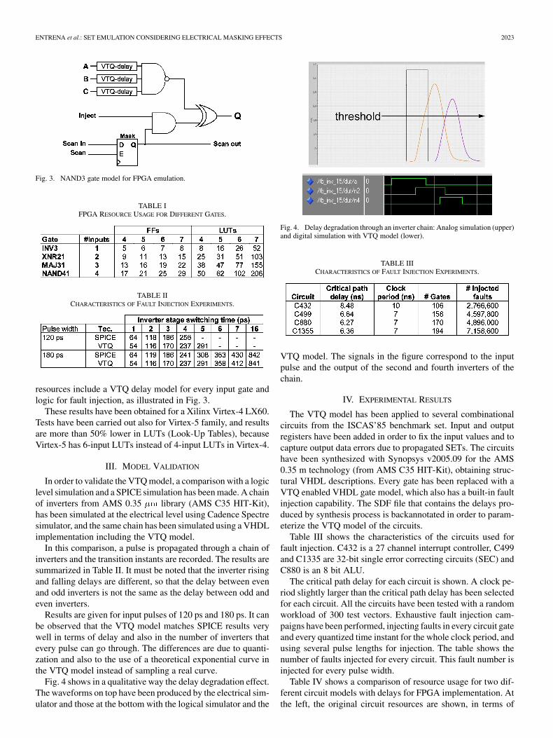
Fig. 3 shows the implementation of a NAND3 gate using theVTQ model considering different delays for every gate input.A non-linear counter is placed at each input in order to captureeach input delay. Finally, a mask flip-flop and two extra gates areadded to support fault injection, similarly to other FPGA-basedfault injection approaches [7], [11]. Mask flip-flops are con-nected in a scan chain and are used to select the fault injectiontarget. Then, a high level pulse asserted at the inject signal pro-vokes a pulse at the output Q for the selected target.
Table I shows resources used by gates with different in-puts, considering different voltage resolutions in bits. These
ENTRENA et al.: SET EMULATION CONSIDERING ELECTRICAL MASKING EFFECTS 2023
Fig. 3. NAND3 gate model for FPGA emulation.
TABLE IFPGA RESOURCE USAGE FOR DIFFERENT GATES.
TABLE IICHARACTERISTICS OF FAULT INJECTION EXPERIMENTS.
resources include a VTQ delay model for every input gate andlogic for fault injection, as illustrated in Fig. 3.
These results have been obtained for a Xilinx Virtex-4 LX60.Tests have been carried out also for Virtex-5 family, and resultsare more than 50% lower in LUTs (Look-Up Tables), becauseVirtex-5 has 6-input LUTs instead of 4-input LUTs in Virtex-4.
III. MODEL VALIDATION
In order to validate the VTQ model, a comparison with a logiclevel simulation and a SPICE simulation has been made. A chainof inverters from AMS 0.35 library (AMS C35 HIT-Kit),has been simulated at the electrical level using Cadence Spectresimulator, and the same chain has been simulated using a VHDLimplementation including the VTQ model.
In this comparison, a pulse is propagated through a chain ofinverters and the transition instants are recorded. The results aresummarized in Table II. It must be noted that the inverter risingand falling delays are different, so that the delay between evenand odd inverters is not the same as the delay between odd andeven inverters.
Results are given for input pulses of 120 ps and 180 ps. It canbe observed that the VTQ model matches SPICE results verywell in terms of delay and also in the number of inverters thatevery pulse can go through. The differences are due to quanti-zation and also to the use of a theoretical exponential curve inthe VTQ model instead of sampling a real curve.
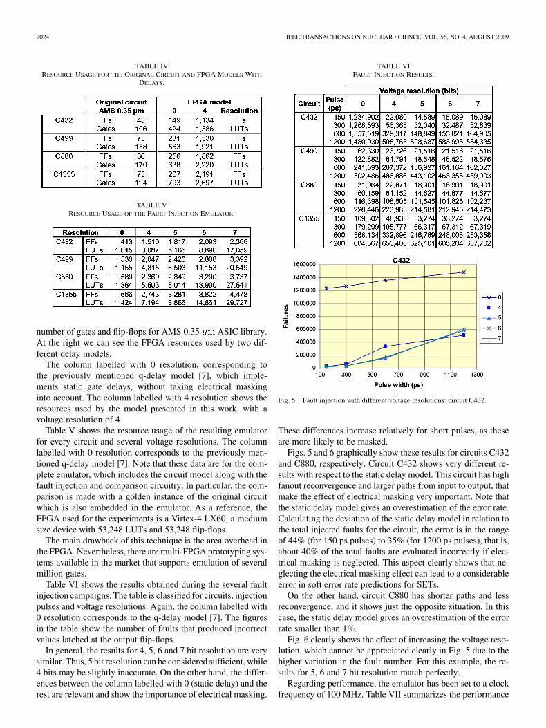
Fig. 4 shows in a qualitative way the delay degradation effect.The waveforms on top have been produced by the electrical sim-ulator and those at the bottom with the logical simulator and the
Fig. 4. Delay degradation through an inverter chain: Analog simulation (upper)and digital simulation with VTQ model (lower).
TABLE IIICHARACTERISTICS OF FAULT INJECTION EXPERIMENTS.
VTQ model. The signals in the figure correspond to the inputpulse and the output of the second and fourth inverters of thechain.
IV. EXPERIMENTAL RESULTS
The VTQ model has been applied to several combinationalcircuits from the ISCAS’85 benchmark set. Input and outputregisters have been added in order to fix the input values and tocapture output data errors due to propagated SETs. The circuitshave been synthesized with Synopsys v2005.09 for the AMS0.35 m technology (from AMS C35 HIT-Kit), obtaining struc-tural VHDL descriptions. Every gate has been replaced with aVTQ enabled VHDL gate model, which also has a built-in faultinjection capability. The SDF file that contains the delays pro-duced by synthesis process is backannotated in order to param-eterize the VTQ model of the circuits.
Table III shows the characteristics of the circuits used forfault injection. C432 is a 27 channel interrupt controller, C499and C1335 are 32-bit single error correcting circuits (SEC) andC880 is an 8 bit ALU.
The critical path delay for each circuit is shown. A clock pe-riod slightly larger than the critical path delay has been selectedfor each circuit. All the circuits have been tested with a randomworkload of 300 test vectors. Exhaustive fault injection cam-paigns have been performed, injecting faults in every circuit gateand every quantized time instant for the whole clock period, andusing several pulse lengths for injection. The table shows thenumber of faults injected for every circuit. This fault number isinjected for every pulse width.
Table IV shows a comparison of resource usage for two dif-ferent circuit models with delays for FPGA implementation. Atthe left, the original circuit resources are shown, in terms of
2024 IEEE TRANSACTIONS ON NUCLEAR SCIENCE, VOL. 56, NO. 4, AUGUST 2009
TABLE IVRESOURCE USAGE FOR THE ORIGINAL CIRCUIT AND FPGA MODELS WITH
DELAYS.
TABLE VRESOURCE USAGE OF THE FAULT INJECTION EMULATOR.
number of gates and flip-flops for AMS 0.35 ASIC library.At the right we can see the FPGA resources used by two dif-ferent delay models.
The column labelled with 0 resolution, corresponding tothe previously mentioned q-delay model [7], which imple-ments static gate delays, without taking electrical maskinginto account. The column labelled with 4 resolution shows theresources used by the model presented in this work, with avoltage resolution of 4.
Table V shows the resource usage of the resulting emulatorfor every circuit and several voltage resolutions. The columnlabelled with 0 resolution corresponds to the previously men-tioned q-delay model [7]. Note that these data are for the com-plete emulator, which includes the circuit model along with thefault injection and comparison circuitry. In particular, the com-parison is made with a golden instance of the original circuitwhich is also embedded in the emulator. As a reference, theFPGA used for the experiments is a Virtex-4 LX60, a mediumsize device with 53,248 LUTs and 53,248 flip-flops.
The main drawback of this technique is the area overhead inthe FPGA. Nevertheless, there are multi-FPGA prototyping sys-tems available in the market that supports emulation of severalmillion gates.
Table VI shows the results obtained during the several faultinjection campaigns. The table is classified for circuits, injectionpulses and voltage resolutions. Again, the column labelled with0 resolution corresponds to the q-delay model [7]. The figuresin the table show the number of faults that produced incorrectvalues latched at the output flip-flops.
In general, the results for 4, 5, 6 and 7 bit resolution are verysimilar. Thus, 5 bit resolution can be considered sufficient, while4 bits may be slightly inaccurate. On the other hand, the differ-ences between the column labelled with 0 (static delay) and therest are relevant and show the importance of electrical masking.
TABLE VIFAULT INJECTION RESULTS.
Fig. 5. Fault injection with different voltage resolutions: circuit C432.
These differences increase relatively for short pulses, as theseare more likely to be masked.
Figs. 5 and 6 graphically show these results for circuits C432and C880, respectively. Circuit C432 shows very different re-sults with respect to the static delay model. This circuit has highfanout reconvergence and larger paths from input to output, thatmake the effect of electrical masking very important. Note thatthe static delay model gives an overestimation of the error rate.Calculating the deviation of the static delay model in relation tothe total injected faults for the circuit, the error is in the rangeof 44% (for 150 ps pulses) to 35% (for 1200 ps pulses), that is,about 40% of the total faults are evaluated incorrectly if elec-trical masking is neglected. This aspect clearly shows that ne-glecting the electrical masking effect can lead to a considerableerror in soft error rate predictions for SETs.
On the other hand, circuit C880 has shorter paths and lessreconvergence, and it shows just the opposite situation. In thiscase, the static delay model gives an overestimation of the errorrate smaller than 1%.
Fig. 6 clearly shows the effect of increasing the voltage reso-lution, which cannot be appreciated clearly in Fig. 5 due to thehigher variation in the fault number. For this example, the re-sults for 5, 6 and 7 bit resolution match perfectly.
Regarding performance, the emulator has been set to a clockfrequency of 100 MHz. Table VII summarizes the performance
ENTRENA et al.: SET EMULATION CONSIDERING ELECTRICAL MASKING EFFECTS 2025
Fig. 6. Fault injection with different voltage resolutions: circuit C880.
TABLE VIIFAULT INJECTION PERFORMANCE.
results obtained for every circuit using this clock frequency.Higher frequencies may be possible as synthesis could be stillbe optimized for speed.
Performance is related with the critical path length of the orig-inal circuit which establishes the circuit clock period, and thetime quantum chosen for the emulation. These two aspects de-termine the number of clock cycles needed by the emulator toapply a single test vector to the combinational circuit in the em-ulation.
The fault injection rates of the SET emulation system rangefrom 571,000 faults/s for C432 to 1,042,000 faults/s for C880in a Virtex-4 LX60 FPGA running at 100 MHz. These ratesare three orders of magnitude faster than a logic simulationapproach [7] and cover electrical masking effects. The perfor-mance improvement is even much higher with respect to elec-trical level simulation.
V. CONCLUSIONS
Analyzing transient pulse propagation in combinational logiccircuits considering electrical masking effects in an efficient and
accurate manner is a difficult problem. The approach proposedin this work provides a solution based on FPGA emulation.A Voltage-Time Quantization model is used to capture delaydegradation effects.
The proposed approach can reach fault injection rates overone million SETs/s, with accuracy close to an analog simulator.
REFERENCES
[1] M. Baze and S. Buchner, “Attenuation of single event induced pulsesin CMOS combinational logic,” IEEE Trans. Nucl. Sci., vol. 44, Dec.1997.
[2] K. J. Hass and J. W. Gambles, “Single event transients in deep submi-cron CMOS,” in Proc. Midwest Symp. Circuits and Systems, 1999.
[3] P. Shivakumar, M. Kistler, S. W. Keckler, D. Burger, and L. Alvisi,“Modeling the effect of technology trends on the soft error rate of com-binational logic,” in Proc.Int. Conference on Dependable Systems andNetworks (DSN), Jun. 2002, pp. 389–398.
[4] F. Wang and Y. Xie, “An accurate and efficient model of electricalmasking effect for soft errors in combinational logic,” in 2nd Workshopof System Effects of Logic Soft Error (SELSE2), Illinois, Apr. 2006.
[5] B. Zhang, W. Wang, and M. Orshansky, “FASER: Fast analysis ofsoft error susceptibility for cell-based designs,” in Proc. 7th Int. Symp.Quality Electronic Design (ISQED), Mar. 2006, pp. 755–760.
[6] B. Zhang, W. Wang, and M. Orshansky, “FASER: Fast analysis ofsoft error susceptibility for cell-based designs,” in Proc. 7th Int. Symp.Quality Electronic Design (ISQED), Mar. 2006, pp. 755–760.
[7] M. G. Valderas, R. F. Cardenal, C. L. Ongil, M. P. García, and L. En-trena, “SET emulation under a quantized delay model,” in Proc. 22ndIEEE Int. Symp. Defect and Fault-Tolerance in VLSI Systems (DFTS),Sep. 2007, pp. 68–78.
[8] M. Violante, “Accurate single-event-transient analysis via zero-delaylogic simulation,” IEEE Trans. Nucl. Sci., vol. 50, Dec. 2003.
[9] Y. S. Dhillon, A. U. Diril, and A. Chatterjee, “Soft-error tolerance anal-ysis and optimization of nanometer circuits,” Proc. Design Automationand Test in Europe (DATE), pp. 288–293, Mar. 2005.
[10] L. Antoni, R. Leveugle, and B. Feher, “Using run-time reconfigurationfor fault injection in hw prototypes,” in Proc. IEEE Int. Symp. Defectand Fault Tolerance in VLSI Systems, 2002, pp. 245–253.
[11] P. Civera, L. Macchiarulo, M. Rebaudengo, M. S. Reorda, and M. Vi-olante, “FPGA-based fault injection techniques for fast evaluation offault tolerance in VLSI circuits,” in Forum on Programmable Logic(FPL), Belfast, Northern Ireland, United Kingdom, Aug. 2001.
[12] C. López-Ongil, M. García-Valderas, M. Portela-García, and L. En-trena, “Autonomous fault emulation: A new FPGA-based accelerationsystem for hardness evaluation,” IEEE Trans. Nucl. Sci., vol. 54, no. 1,Feb. 2007.
[13] M. J. Bellido-Diaz, J. Juan-Chico, A. J. Acosta, M. Valencia, and J.L. Huertas, “Logical modelling of delay degradation effect in staticCMOS gates,” IEEE Proc. Circuits, Devices & Systems, vol. 147, no.2, pp. 107–117, Apr. 2000.