Embed Size (px)
Citation preview

SERVO TESTER
MINI CIRCUITS
WEATHER SA FELLITE CHANNEL SWI7 tiIING UNIT
DIGITAL CAPACITANCE METER
1808 CPU CARD


OM1A1PLIN/PROIECTS
BOOK TWENTY
EDITORIAL
I'Maplin Projects Book Twenty Three' is a compilationof the projects from 'Electronics- The MaplinMagazine, Issue 23', which is now out of print. Otherissues of 'Electronics - The Maplin Magazine' will bereplaced by projects books as they go out of print. Forkit prices, please consult the latest Maplin catalogueand free price change leaflet, order as CA99H.
I Editor Robert Ball I Compiled by Mike HolmesI Technical Editors Dave Goodman. Chris Barlow. Gavin Cheeseman,
Tony Bricknell. Alan Williamson.
I Technical Author Martin PipeI Technical Artists John Dudley, Lesley Foster. Paul Evans.
Ross Nisbet Nicola Hull.
I Art Designers Peter Blackmore, Jim BowlerI Published by Maplin Electronics plc.
Printed by: Mayhew McCrimmon Printers LtdI Mail Order P 0 Box 3. Rayleigh. Essex SS6 8LR
I Telephone Retail Sales: (0702) 554161.I Retail Enquiries: (0702)552911.I Trade Sales: (0702) 554171
I Cashtel: (07021552941I General: (0702) 554155I Shops: See below.I Fax: (0702)553935 I Telex: 995695
Visit a Maplin Shop for Personal Service
You'll Find Maplin Service in:Birmingham, Sutton New Road. Erdington.Telephone: (021)384 8411.Brighton, 65 London Road.Telephone. (0273) 620930.Bristol, 302 Gloucester Road.Telephone. (0272) 232014.Cardiff, 29-31 City Road.Telephone: (0222)464554.Chatham, 2 Luton Road.Telephone: (0634) 818588.Glasgow, 264-266 Great Western Road.Telephone: (041)353 3323.Leeds, Carpel World Building, 3 Regent Street.Telephone: (0532)449200.Leicester, Office World Building, Burton Street,Telephone. (0533) 623288,London, 146-148 Burnt Oak Broadway. Edgware.Telephone: (081) 951 0969,London, 120-122 King Street, Hammersmith,Telephone: (081) 748 0926.Manchester, 8 Oxford Road.Telephone: (061)236 0281.Newcastle-upon-Tyne, Unit 4, Allison Court,The Metro Centre, Gateshead.Telephone: (091) 461 0022.Nottingham, 86-88 Lower Parliament Street.Telephone: (0602)410242.Reading, 129-131 Oxford Road.Telephone: (0734) 566638.Sheffield, 413 Langsett Road, Hillsborough.Telephone: (0742) 855492.Southampton, 46-48 Bevois Valley Road.Telephone: (0703)225831.Southend-on-Sea, 282-284 London Road, Westcliff -on-SeaTelephone: (0702) 554000.
All our shops are open from 9.00am to 5.30pm Monday toFriday (9.30am Friday). In addition Manchester is openSundays if local conditions permit. All shops are closed torPublic Holidays. Shops do not close for lunch.
PROJECTS
CAPACITANCE TESTER , SERVO TESTERI Shows capacitance values from 100pF
46/
I Measures the performance of RC servos2to 99 9µF on a 3 -digit LED display. as an aid to fault finding. Uses standard
20ms frame rate.
Fin,11AB basMEedcardTORE RCPU used as the1
ti Frame Store for the MAPSAT WEFAXWeather Satellite System.
Copyright All material is sublect to worldwide copyright protection and
reproductioi or imitation in whole or part is expressly forbidden
All reasonable care is taken to ensure accuracy in preparation of the
magazine. tut Maplin Electronics plc cannot be held legally responsible
for its contents Where errors occur corrections wit, be published as soon
as possible afterwards Permission to reproduce printed circuit boardlayouts commercially or marketing of kits must be sought from the
publisher
c Copyright 1992 Maplin Electronics plc.
9g DOWN CONVERTER
Lk/ PART 21 The Channel Switching Unit for the
MAPSAT VHF receiver and decoder, plus
installation and testing the complete system.
S7,wirpovRemEentMAlaIrNmIsCtepIRpeCryotIoTrriver,
Pink Noise Generator, Optical Port Data
Link, Metal Effects Unit.
FOR MAIL-ORDER ENQUIRIES, PLEASE DO NOTCALL OUR SHOPS AS THEY WILL BE UNABLETO HELP YOU.Send all mail to: P.O. Box 3, Rayleigh, Essex, SS6 8LR.
G TAL
CAPAC TANCE
METERby Robert Penfold
Practically every constructionalproject includes a number of capacitors,and the ability to test these componentsis a decided assett for any electronicsconstructor. Unfortunately, testingcapacitors properly is something that isbeyond the capability of mostmultimeters and other items of testequipment that are likely to be found inthe average amateur electronicsworkshop. It is possible to make a fewrough checks on capacitors using manyanalogue multimeters, and some modernoscilloscopes have a built-in componenttester function that can be used to givesome idea of a test capacitor's value, butfor accurate measurement of capacitancea proper capacitance meter is required.
This design has a three digit LEDdisplay, and it covers five ranges whichare as follows: -
Range 1 0 to 9.99nFRange 2 0 to 99.9nFRange 3 0 to 999nFRange 4 0 to 9.99µFRange 5 0 to 99.91.4.F
This coverage includes all thecommon values, but the unit cannotmeasure very low values of just a fewpicofarads, or high value electrolyticcomponents. In practice this is not likelyto matter too much as very low valuecomponents are little used in moderncircuits, and large values can bechecked by using two components wiredin series, as will be explained more fullylater in this article. An overflow indicatorLED is included so that misleadingresults are avoided if an unsuitable rangeis selected. The unit is powered from aninternal 9 volt battery, and is inconsequence fully portable.
Test °Cap 0 Monostable
Clock
L. F.
Osc.
Gate
ControlLogic
Decade
Counter
Latch
Decade
Counter
Latch
Decade
Counter
Latch
OverflowInd.
Figure 1. Block schematic.
2
R4470k
+5V
IC2b4001BE
IC2a4001BE
1 3
OV
1 C2470uF
IC34017BE
D. P. D.P.Display 1 Display 2 RV'
999 99uF
9.991FS1a
99 9uF
16
T
/ ITo IC4 pins
R5
12.13814 10M
F
C3100nF
IF-
11
8 3 15 2
Reset
1 47k
R1560R
10k
R333k
999nrR2
C1
1nF
2
R61M
IC1555
To 1C9
I, I
IC4a Sib4001BE
FT-. Latch.1".8
IR7 R8 R9100k 10k 1k
IC4c4001BE
5
6 )
1
C64n7FI
IC4b4001BE SKI SK2 SK3 SK4
To IC4 +
pin 7 Tes Dis. Cal.t Cap.
IC57805
pin 9
Out
iC4TicL
CornF
In
S2ON/OFF
-c5T100nF
B1
9V
Figure 2. Clock, control and monostable circuit.
3
IC2c4001BE
13
To IC2 pa, 14
10 1
9
IC2c1
ri R10470R
up,
16 F15
IC640138E
7 8 9 10
3 10
To IC2 pin 7
16
IC740110BE
6
11824111111
947
8
R11-17All 470R
MITT9T0
51
Sta
Display 1
106
IC8401108E
69
4
121
-171-6I-5TIT0
R18-24All 470R
5
Sta
Display 2
10
IC94 0110BE
6
11r1171121
e. Latch
e. Reset
5V
9 To ICI4 pin 31
R25 -31All 470R
TT61-41-2T-191-10
3 Display 3
OV
Figure 3. Counter and overflow indicator circuit.
System OperationIn common with most capacitance
measuring devices, this one operates byusing the test component as thecapacitive element in a C -R timingnetwork. In this case the timing networkforms part of a monostable multivibrator,and the higher the value of the testcomponent the longer the output pulse ofthis circuit. There is a linear relationshipbetween the value of the test componentand the output pulse duration, and thismakes it relatively easy to employ thepulse in controlling a display circuit thatgives a reading directly in nanofarads ormicrofarads (nF or /IF). The blockdiagram of Figure 1 helps to explain theway in which the unit functions.
A low frequency oscillator controlsthe rate at which readings are taken, andthis gives readings at just under onesecond intervals. The output of theoscillator drives a simple control logiccircuit, and this provides pulses thatsequence the rest of the circuit correctly.The first operation in the sequence is fora trigger pulse to be sent to themonostable multivibrator, and this thengenerates an output pulse that is used asthe gate pulse for a clock oscillator and athree digit counter circuit. The longer thegate pulse, the higher the count value thatthe display will reach at the end of thegate pulse, where the count is 'frozen'. Inpractice, the clock frequency is adjustedso that the display readings are accuratecapacitance values. With a three digitcounter only a rather restricted range ofvalues can be accommodated with goodaccuracy, and so the monostable isequipped with five switched timingresistors. These give the unit its fivemeasuring ranges, and enable a widerange of values to be catered for.
The counter circuit is ofconventional design, having latches andseven segment decoder/drivers. Thevalue held within the counters istherefore not displayed immediately, butis held in the counters until the controllogic circuit provides the latches with a
latching pulse. The new value is thendisplayed, and remains displayed evenwhen the control logic circuit sends areset pulse to the counter circuit. Thisreset pulse is essential as it is needed toensure that the counter starts at '000'when the next gate pulse commences.The point of including the latches insteadof driving the decoder/drivers directfrom the counters is that it permits acontinuous display to be provided.Without the latches the reset andcounting action would be displayed,which would give unacceptable results inpractice.
If the test capacitor has a valuewhich is beyond the full scale value of therange in use, the counter circuit will gothrough one or more complete cycles,and will display an erroneous result. Toprevent the user from being misled, anoverflow indicator circuit is included,and this simply switches on an LEDindicator if a complete output cycle isproduced by the final decade counterstage. A full output cycle is onlyproduced from this stage if it cyclesthrough a complete 0 to 9 count and thenback to zero again.
Circuit OperationFigure 2 shows the circuit diagram
for the clock oscillator, low frequencyoscillator, control logic, and monostablestages of the unit. The counter/driver andoverflow circuit is shown separately inFigure 3.
Starting with Figure 2, IC5 is a 5 voltmonolithic voltage regulator which givesa well stabilised 5 volt output from the 9volt battery supply. All circuitry ispowered from the stabilised 5 volt supplyrail. The battery needs to be a fairly highcapacity type (such as six HP7 size cellsin a plastic holder) as the currentconsumption of the circuit is quite high ataround 85 mA. The current consumptioncan exceed 100mA when most or all ofthe display segments are driven, and forthis reason a low power voltage regulatoris inadequate for the IC5 position.
The low frequency oscillator isbased on IC2a and IC2b which are CMOSNOR gates. However, in this circuit theyare wired as simple inverters and areused in a standard CMOS astableconfiguration. Note that the operatingfrequency of the oscillator is much higherthan the frequency at which readings aretaken, since ten output cycles areneeded from this oscillator in order tocomplete one reading cycle.
IC3 and IC4a form the control logicblock. IC3 is a CMOS 40178E one -of -tendecoder, and this has ten outputs ('O' to'9') which each go high, in sequence, fora single input cycle. In this circuit output'0' provides the reset pulse to thecounters. Output '1' then goes high andtriggers the monostable which generatesthe gate pulse for the clock/countercircuit. Outputs '2' to '8' are unused, andthe period during which these go highprovides time for the gate pulse to finishand the count to be completed. Output '9'provides the pulse that latches the newreading onto the display, but a negativelatching pulse is required. IC4a istherefore used to invert the signal so as togive a suitable pulse. The timingdiagram, Figure 4, shows the sequence ofevents and may help to clarify operationof the unit.
The monostable multivibrator is aconventional CMOS type which is formedfrom two 2 input NOR gates (IC4b andIC4c). Although a very simple form ofmonostable, it has characteristics whichmake it well suited to the presentapplication. It is a non-retriggerabletype, and consequently it can provide anoutput pulse that is shorter than thetrigger pulse from IC3. This is important,as with a retriggerable type the minimumdisplay reading would be quite high. Theself capacitance of the circuit is quitelow, and this is important as a high levelof local capacitance would upset thelinearity of the circuit, and would give alarge minimum display reading. On theprototype the display reads '000' on allfive ranges with no test capacitor connected.
4
LF. OSC,
RESET
TRIGGER
LATCH
GATE PULSE
CLOCK
Figure 4. Timing diagram.
R5 to R9 are the range resistors, andby reducing the timing resistance indecade steps the timing capacitanceneeded for a given reading is boosted indecade increments. Provided the rangeresistors have a tolerance of 1% orbetter, this arrangement seems to giveconsistent results, and there is no need tohave each range individually calibrated.RI and S la are used to drive the decimalpoint segment of the appropriate display,except on Range 3 (999nF) where nodecimal point indication is needed.
The clock oscillator is a standard 555astable circuit. RV1 controls the clockfrequency, and this is used to calibratethe unit. The output of the monostabledrives pin 4 of IC 1, and the clockoscillator is only operative during thegate period. This avoids the need for aseparate signal gate.
Turning our attention to Figure 3now, the counter circuit is based on threeCMOS 40110BE devices. These areperhaps not the best known of the CMOSlogic family, but they are very versatilecomponents which deserve greaterusage. They are actually up/downcounters with separate clock inputs andcarry/borrow outputs. As it happens theability to operate in a down counter modeis of no value here, and the down clockinput is simply tied to the negative supplyrail. The three counters are wired inseries to give a standard three digitdisplay, with IC9 providing the leastsignificant digit and IC7 furnishing themost significant digit. The 40110BEcontains a decade counter, a sevensegment decoder, and a latch/displaydriver circuit. Each chip can thereforereplace a standard three chip TTL stylecounter/driver/latch arrangement. Theoutputs can directly drive a commoncathode seven segment LED display and,unusually for a CMOS logic device, ahigh drive current is available from each
output. Even with a supply potential ofjust 5 volts it is essential to drive eachdisplay segment via a current limitingresistor in order to keep the currentconsumption of the unit down to areasonable level.
The 'carry' output of IC7 is fed to theclock input of IC6, which is a dual D typedivide by two flip/flop, but in this circuitonly one section of the device is utilised.The output of IC6 changes state in theevent of an overload, but with a severeoverload there could be several outputcycles from IC7. Directly driving the LEDindicator LED1 from IC6 would not betotally satisfactory, since this output istransitory and the LED might only giveone or two brief flashes which couldeasily be missed. To avoid this the outputof IC7 is used to drive a simple set/resetbistable circuit formed from twootherwise unused gates of IC2, and thelatch drives LED indicator LED1. Both IC6and the latch are reset from IC3 so thatthe overflow circuit starts afresh when anew reading is taken.
Safety FirstSimple but important additions to the
circuit (in Figure 2) are the two extrasockets at the input (SK3 and SK4) andcapacitor C6. The purpose of SK3 is toenable test components to be dischargedbetween SK1 and SK3 prior to connectingthem across SKI and SK2 and making ameasurement. This applies only tocomponents which have been in use in acircuit and might contain a residualcharge prior to testing. Higher valuetypes which have been used in fairly highvoltage circuits are the ones which aremost likely to cause problems. Of course,in extreme cases capacitors must beslowly discharged through a bleed'resistor before removing them from thecircuit. This is as much for your ownprotection as for that of the capacitance
meter, and great care must be exercisedwhen dealing with charged, high voltagecomponents of other than very lowvalues. Building a protection system intothe meter input circuit was considered,but it is difficult to produce a reallyeffective circuit that does not impair theperformance of the unit. This simplealternative was therefore considered tobe the more practical solution to theproblem.
C6 is a built-in calibration capacitor.This is not an essential part of the unit,but it is handy when initially calibratingthe unit, and therafter it is very useful tohave a calibration component that isalways immediately available for testingpurposes. If a test component gives asLghtly erroneous reading it is then just amatter of switching to range 1,connecting SK2 to SK4 to connect C6 intocircuit, and then checking that a validreading is obtained (4.70nF). A word ofwarning is due here though, and this issimply to point out that the meter itself isonly likely to be accurate to within acouple of percent or so, except at valuesequal to or close to the calibration value.Another point to bear in mind is that thevalues of capacitors are dependent ontemperature and other factors. If a testcomponent should happen to give areading that is in error by slightly morethan its tolerance, this probably meansthat it is perfectly satisfactory rather thanfaulty.
ConstructionVirtually all the components fit onto
the printed circuit board, and details ofthe board are provided in Figure 5.Construction of the board is notparticularly difficult, but there are a fewpoints which should be borne in mindwhen assembling it. The main point tonote is that, apart from IC1 and IC5, theintegrated circuits are CMOS types, and
5
00IC4
IC3
a
cc
IC2
R10
CD CO rs 4.0CC CC CC CC CC
11111
IC6
0 0 0 0 0 0
DISPLAY 1 DISPLAY 2
R3
DISPLAY 3
CO
1E1 11111Fil?,CO Cc
NInNNN C9
cc+ccmcc
0c21,7c -ccc
0
0
IC5OOOO
I I I
:
a'aec7-50 Djar-/431-ill 171-0- ° \sD ro r: (r-7:
0_
(131 I 142Q)-10JR-Vaaes0
_00000 101'10'1° 117'011° ITI0I01100
1_20 1 I II ' I I
Leri
I/-91 r1 t
all wai---4T--alli FD-i-401,e.j
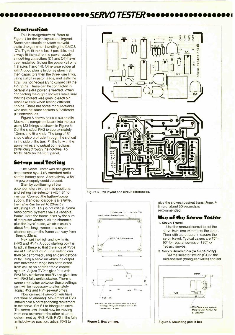
Figure 5. PCBlayout and component references.
are therefore vulnerable to damage bystatic charges. To avoid this they shouldbe fitted in integrated circuit holders, butnot be plugged into circuit until the boardhas been completed and wired to theoff -board components (see Figure 6).Until then they should be left in theanti -static packaging. Handle the devicesas little as possible when fitting them intothe holders, and be particularly carefulwith the three counter ICs, which are notthe cheapest of CMOS devices. If in anydoubt, or you are not an experiencedconstructor, then read the Constructor'sGuide leaflet supplied with this kit.
IC5 is mounted horizontally on theboard and it is a good idea to use a short6BA or M3 screw and matching nut to fixit securely to the board.
The three seven segment LEDdisplays are mounted in holders whichhelp to raise them to a suitable heightabove the surface of the board as well asreducing the risk of heat damage whenconnecting them. Suitable ten pin holdersseem to be unavailable, but it is notdifficult to improvise suitable holdersfrom three ordinary 14 -pin DIL integratedcircuit holders. First the holders are cutin half lengthwise using a hacksaw to
give six seven pin SIL types. The pins ateach end of the holders are then pushedout using pliers or simply trimmed offusing wire clippers. This leaves six 5 -pinSIL holders which can be used for thedisplays. The spacing between thedisplays is sufficient to make itunnecessary to trim off the excess piecesat each end of the holders.
Pins are fitted to the board at thepositions where connections to off -boardcomponents will be made. There are anumber of link wires (sixteen in fact) andthese are made from about 22 s.w.g.enamelled copper wire, or trimmings
6
C6
eSK4 SK 2 + SK3 - SK1
Link
8 9 1011
S1LED1
Shortlead
S2
0
0 0 10 0 0 0 0
Display 1 Display 2 Display 3
O
O
O
0
0
0
131
Clip
Red Black
Figure 6. Wiring.
from resistor lead -out wires can be used.A Verocase having approximate
outside dimensions of 205 by 140 by 40millimetres makes a good housing forthis project. It is used vertically with adisplay window cut in the front panel(which would normally be the top panel),while the controls and sockets aremounted on the top panel (which wouldusually be the front of the case). Theprinted circuit board is mounted on therear panel using one inch long 6BAscrews and half inch spacers, which areneeded to bring the fronts of the displaysclose to the display window. The board ispositioned well towards the bottom lefthand corner of the unit so as to bring thedisplay close to the middle of the front
I
panel. The display window mustobviously be positioned accurately infront of the display, and it can be cutusing a fretsaw, coping saw, or aminiature round file. A piece of reddisplay filter is glued in place over orbehind the cutout, and any generalpurpose material is suitable for this. Notethat the Maplin display filter material hasan anti -glare finish on one surface, andthis less reflective surface should be theone that faces forward or outwards.
On the prototype SKI to SK4 are 1millimetre sockets mounted with about9.5 millimetres spacing. C6 is mounteddirect across SK3 and SK4 so as tominimise stray capacitance, andpreserve good accuracy at low readings.
7
140
34
172162
152142
17
3065
89.598.5
197
FRONT
33
1
90
17
Top view
-0
0L
E
61
F
52
29144
205
45 j70 67
REF. SIZE
A 05.2B 05C 03D o9.5E 03.2
All sizes in millimetersScale = 1:2
1
38
37
36
Drilling details.
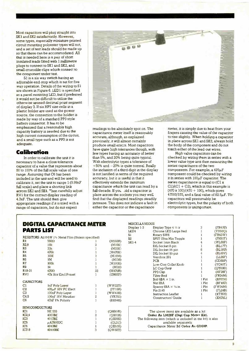
Most capacitors will plug straight intoSKI and SK2 satisfactorily. However,some types, especially miniature printedcircuit mounting polyester types will not,and a set of test leads should be made upso that these can be accommodated. Allthat is needed here is a pair of shortinsulated leads fitted with 1 millimetreplugs to connect to SKI and SK2, andsmall crocodile clips which connect tothe component under test.
Si is a six way switch having anadjustable end -stop which is set for fiveway operation. Details of the wiring to Siare shown in Figure 6. LED I is specifiedas a panel mounting LED, but if preferredit would not be difficult to utilise theotherwise unused decimal point segmentof display 3. If six HP7 size cells in aplastic holder are used as the powersource, the connection to the holder ismade by way of a standard PP3 stylebattery connector. It has to beemphasised that a reasonably highcapacity battery is needed due to thehigh current consumption of the circuit,and a small type such as a PP3 is notadequate.
CalibrationIn order to calibrate the unit it is
necessary to have a close tolerancecapacitor of a value that represents about50 to 100% of the full scale value of onerange. Assuming that C6 has beenincluded in the unit and will be used tocalibrate it, set the unit to range 1 (9.99nFfull scale) and place a shorting linkacross SK2 and SK4. "len carefully adjustRV1 for the correct display reading of4.7nF. The unit should then giveappropriate readings if it is tried with arange of capacitors, but do not expect
readings to be absolutely spot on. Thecapacitance meter itself is reasonablyaccurate, although, as explainedpreviously, it will almost certainlyproduce small errc:s. Most capacitorshave quite high tolerances though, withfew types having an accuracy of betterthan 5%, and 20% being quite typical.With electrolytic types a tolerance of+50% and -20% is quite normal. Reallythe inclusion of a third digit in the displayis not justified in terms of the requiredaccuracy, but it is useful in that iteffectively extends the minimumcapacitance which the unit can read by afull decade. If yot. old a capacitor inplace across the sockets you may wellfind that the displayed readings steadilyincrease. This does not indicate a fault ineither the capacitor or the capacitance
meter, it is simply due to heat from yourfingers causing the value of the capacitorto rise slightly. When holding a capacitorin place across SKI and SK2, always holdthe body of the component and do nottouch either of the lead -out wires.
High value capacitors can bechecked by wiring them in series with alower value type ana then measuring theseries capacitance of the twocomponents. For example, a 470/.11component could be checked by wiringit in series with 100m.F capacitor. Theseries capacitance is equal to (C1 xC2)/(C1 + C2), which in this example is(470 x 100)/(470 + 100), which gives47000/570, and a final value of 82.5µ.F. Thrcapacitors will presumably beelectrolytic types, but the polarity of bothccmponents is unimportant.
DIGITAL CAPACITANCE METER MISCELLANEOUS
PARTS LISTDisplay 1-3 Display Type 4'ii 3 (FR41U)LED1 Chrome LED Large Red 1 (YY60Q)Si Rotary SW6 1 (FH43W)
RESISTORS: All 0.6W 1% Metal Film (Unless specified) S2 SPST Ultra MM Toggle 1 (FH97F)R1
R2,8R3
560f110k33k
1
21
(M560R)(M1OK)(M33K)
SKI -4 Socket lmm Black 4 (WL59P)DIL Socket 8 -pin 1 (BL17T)DIL Socket 14 -pin 6 (BL18U)
R4 470k 1 ;M470K) DIL Socket 15 -pin 4 (BL19V)R5 IOM 1 (M1OM) Verobox 201 1 (LLO5F)R6 1M 1 (M1M) PCB 1 (GD59P)R7 100k 1 :M100K) Low -Cost Collet Knob 1 (YG40T)R9 lk 1 (M 1K) LC Cap Grey 1 (QYO3D)R10-31 47011 22 (M470R) PP3 Clip 1 (HF28F)RV1 47k Hor Encl Preset 1 (UHO5F) Filter Red 1 (FR34M)
Bolt 6BA x 1 in. 1 Pict (BFO7H)CAPACITORS Nut 6BA 1 Pict (BF18U)CIC2C3C4,5
lnF Poly Layer470µF 16V PC Elect100nF Poly Layer100riF 16V Minidisc
1
1
1
2
(WW22Y)(FF15R)
(WW41U)(YR75S)
Spacer 6BA x 1/4 in. 1 Pkt (FW34M)Pin 2145 1 Pkt (FL24B)Instruction Leaflet 1 (XT76H)Constructors' Guide 1 (XH79L)
C6 47nF 1% Polysty 1 (BX64U)
SEMICONDUCTORSICI NE 555 1 (QH66W) The above items are available as a kit:IC2,4 4001BE 2 (QX01B) Order As LNI28F (Digi Cap Mete Kit).IC3 4017BE 1 (QX09K) The following item (which is included in the kit) is alsoIC5 kiA7805UC 1 (QL31J) available separately.IC6 4013BE 1 (QX07H) Capacitance Meter Bd Order As GD59P.IC7-9 40110BE 3 (QW68Y)
9
PART 1
* Fast 6 MHz CPU* 64K/256K RAM* 7 Decoded I/O
Select Lines
by Mark Brighton
Z8OB CPU CARDThis article describes the first part of
a modular Z80 based micro -controllersystem, designed to meet the needs of awide range of control monitor and displayapplications, where it is often notdesirable to dedicate a home micro to asingle task. Some applications for thesystem will be presented in future issuesof "Electronics", the first being as part ofa video display for WEFAX weather sat-ellite pictures, received by the "Mapsat"Receiver/Decoder System, described inprevious issues.
Two expansion modules are underdevelopment at the time of writing, aparallel/serial I/O card using the Z80 SIOand DART peripheral chips, and a highresolution graphics card using theYamaha/Microsoft V9938 MSX graphicsprocessor. These modules will beconnected to the Z8OB CPU card bymeans of a common motherboard, thewhole system being in eurocard format.
The modules themselves will beequipped for expansion, being suppliedas a basic kit, with optional extra parts tobring them up to full capability. In thisway it is hoped that the system may betailored by the user to suit his/herparticular application (and finances!),without the built in redundancy that oftenresults from using 'off-the-peg' com-puters (high resolution colour graphicsand six octave polyphonic sound are alittle excessive for a central heatingcontroller or a home security system!).
The CPU card described here is noexception to the expandable concept justout -lined, being supplied in basic form asa 'bare bones' minimum computer circuitwhich forms the foundation module of
10
'6888'8.'288
I -
. . .
warms.:
II!
1-1-1611.-Tzlz;
arrararrasZ
21111111111
.. 17'vvvW228R8519
a,j1W41111711111 111111I mut
V.V. V "0611 2a222P. 31M
II1 IP 2,
e.;
31
.1=
EE
7D,
7. 2
--0
/ I
ofvT
al
2 ;la
4-11imIg,w11111111111111111,
7_16'
a
gi araarsarisif
a
.0
Figure 1. Circuit Diagram.
11
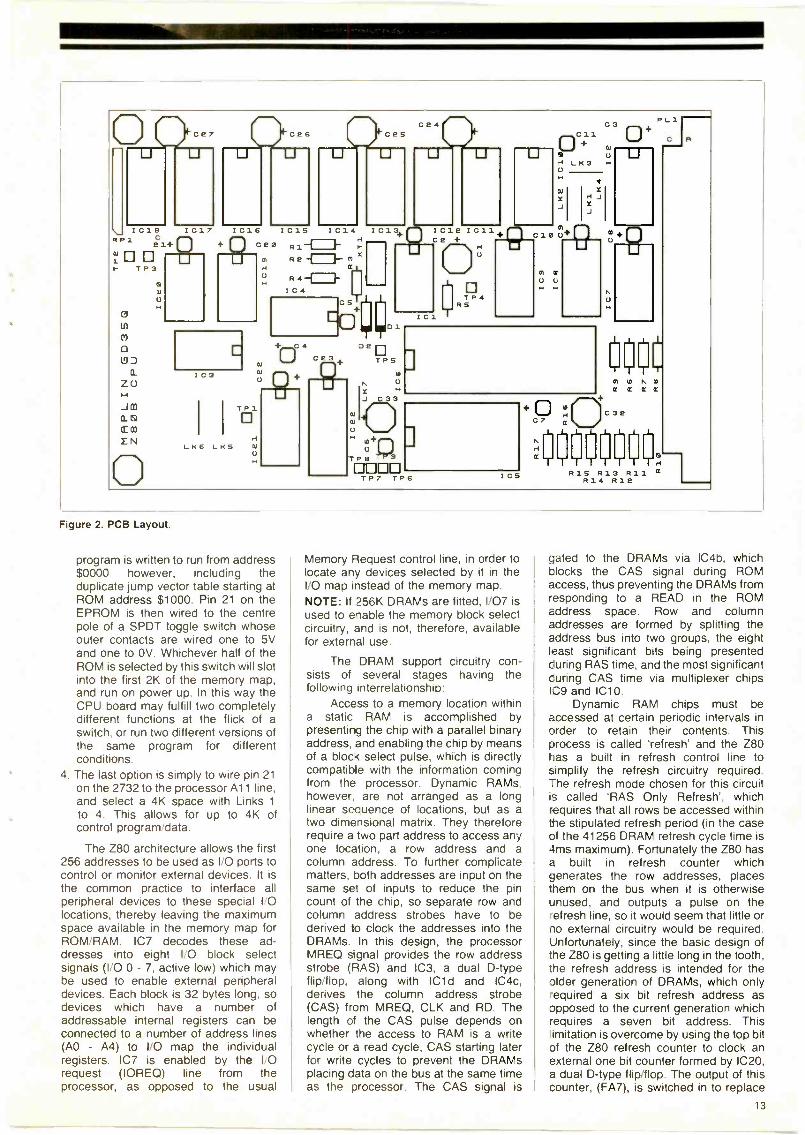
any dedicated system built up by theaddition of a combination of expansionmodules. Optional parts for this boardconsist of a number of logic chips whichprovide all the multiplexed address andrefresh circuitry for dynamic RAMs, withlinking options to enable the use of 64Kor 256K DRAMs. The operation of thesecircuits will be covered at the end of thefollowing basic circuit description.NOTE: Only the basic kit is required forthe WEFAX Frame Store.
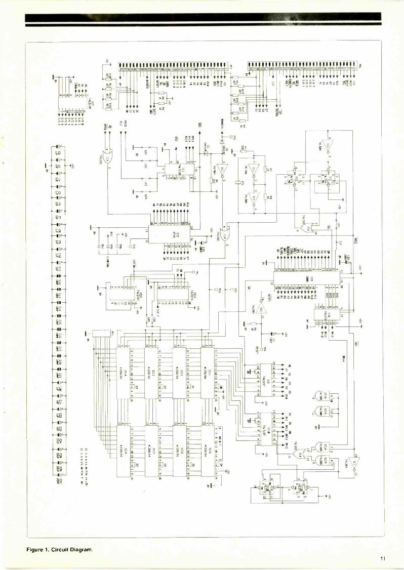
Circuit DescriptionThe heart of the circuit, shown in
Figure 1, is a Z8OB CPU chip (IC6)running at 6.144MHz, which makes it halfas fast again as its older brother theZ80A, still to be found in many popularpersonal computers. The clock circuit isformed by inverters IC1a and IC1b, R1,R2, R3 and XT1, and provides a systemclock on the edge connector, as well asclocking the column address strobe(CAS) generator IC3 (if fitted). If anexternal system clock signal is available,Link 7 may be omitted and the externalclock connected to the system clock pinon the edge connector (PA1.25). Thisshould be a single phase square waveclock with a 50/50 mark/space ratio.RESET for the processor (and any otherboards connected to the system) isprovided via inverter IC1e by RC networkR5/C1. An active high reset signal maybe input on reset pin TP4 to Cold Startthe system.
The four most significant addresslines out of the processor (Al2-A15) arebuffered by IC8, a dual two bittransparent latch clocked by the MemoryRequest (MREO) line from the CPU. Thebuffered products BA12-BA15 are takento an address decoder chip IC2, whichprovides two memory mapped ROMselect lines BS1, starting at $0000 andBS2 starting at $2000. These blocks maybe 2K, 4K or 8K long, depending on thepositions of links 1 to 4 (see Table 1).NOTE: If an external ROM RAM is to beenabled by BS2, the RAM disable line(RAMDIS) should be connected to BS2to avoid contention on the data bus(BS1 is already so connected, beingused to enable the internal ROM).
The internal ROM position IC5 is a24 -pin standard 'byte -wide' pin -out andwill accept single rail 2716 or 2732EPROMs. When buying ROMs for thisboard, bear in mind that they will have tohave an access time less than or equal
1
2K4KBK
j = Fit Link
LINK2 3 4
x
x x
x = No Link
x
Table 1.
LINK0 1. TP6 - TP8PT 2. TP6 - TP7O 3. TP6 - SWITCH*S 4. TP6 - TP9`See Text
Table 2.
to 250ns when running the system at themaximum clock speed of 6.144MHz. Inpractical terms this may mean that it isnot possible to use a 2716 at full clockspeed, since it is usually only availableup to about 350ns access time, but asthe board will function quite normally atany clock speed less than maximum,some lower speed applications will suitthe 2716 ROM's less frantic way of lifeadmirably.
The function of IC5, pin 21, variesdepending on the type of ROM fitted, andseveral strapping options have thereforebeen provided (see Table 2). For thesake of clarity I will summarise theoptions provided as follows:
1. When using a 2716 EPROM pin 21(Vpp) should be connected to +5Vduring normal use.
2. If using a 2732 for reasons of speedalone, where less than 2K of space isneeded for the control program, pin21 (A11) may be linked to OV andLinks 1 to 4 wired to select a 2KROM. Only the low half of the ROM isthen used, which results in an extra8K of RAM being available if 256KDRAMs are fitted, since the ROMoverlays the first 2, 4 or 8K of each64K block of RAM. This isunavoidable, due to the 64K addressrange of the Z80, and the need tohave the control program accessableto the processor at any time,regardless of which block of RAM isselected.
3. When using a 2732 for programs lessthan 2K in length, it is possible to treatthe two halves of the ROM asseparate "SUBROMs", as follows.Two separate programs aredeveloped and burnt into the EPROMalong with their jump vector tables ifrequired. The first, in the lower half ofthe ROM, is jumped to by means ofthe cold start vector, at address$0000, in the normal way. Thesecond program is burnt into theupper half of the EPROM, from ROMaddress $1000 onwards. The
12
RP1I C18
C21+
0 0TP3
Ln
00
0_
Z 0
JMCL G
CO0
EN
0
C27
I C17 I C16
ces
I C15 1014 I
coo Ri
Is RE
I 03
TP1
rl
LKS
R4I 04
CS
FrnC4
U Ce3 +
01
DeoTPS
tO
C33
C11
0 +LK3
LIJ
C18 ri+
01 CO
U
S
" 094nT1667:09
TP7 TP6 ICS
C3
U
c3e
R14 Rie
PL1
Figure 2. PCB Layout.
program is written to run from address$0000 however, including theduplicate jump vector table starting atROM address $1000. Pin 21 on theEPROM is then wired to the centrepole of a SPDT toggle switch whoseouter contacts are wired one to 5Vand one to OV. Whichever half of theROM is selected by this switch will slotinto the first 2K of the memory map,and run on power up. In this way theCPU board may fulfill two completelydifferent functions at the flick of aswitch, or run two different versions ofthe same program for differentconditions.
4. The last option is simply to wire pin 21on the 2732 to the processor Al 1 line,and select a 4K space with Links 1to 4. This allows for up to 4K ofcontrol programidata.
The Z80 architecture allows the first256 addresses to be used as I/O ports tocontrol or monitor external devices. It isthe common practice to interface allperipheral devices to these special t 0locations, thereby leaving the maximumspace available in the memory map forROM/RAM. IC7 decodes these ad-dresses into eight 1,0 block selectsignals (I/O 0 - 7, active low) which maybe used to enable external peripheraldevices. Each block is 32 bytes long, sodevices which have a number ofaddressable internal registers can beconnected to a number of address lines(AO - A4) to I/O map the individualregisters. IC7 is enabled by the I 0request (IOREQ) line from theprocessor, as opposed to the usual
Memory Request control line, in order tolocate any devices selected by it in the110 map instead of the memory map.NOTE: If 256K DRAMs are fitted, 1/07 isused to enable the memory block selectcircuitry, and is not, therefore, availablefor external use.
The DRAM support circuitry con-sists of several stages having thefollowing interrelationship:
Access to a memory location withina static RAM is accomplished bypresenting the chip with a parallel binaryaddress, and enabling the chip by meansof a bloc< select pulse, which is directlycompatible with the information comingfrom the processor. Dynamic RAMs.however, are not arranged as a longlinear sequence of locations, but as atwo dimensional matrix. They thereforerequire a two part address to access anyone location, a row address and acolumn address. To further complicatematters, both addresses are input on thesame set of inputs to reduce the pincount of the chip, so separate row andcolumn address strobes have to bederived to clock the addresses into theDRAMs. In this design, the processorMREQ signal provides the row addressstrobe (RAS) and IC3, a dual D -typeflip/flop, along with IC1d and IC4c,derives the column address strobe(CAS) from MREQ, CLK and RD. Thelength of the CAS pulse depends onwhether the access to RAM is a writecycle or a read cycle, CAS starting laterfor write cycles to prevent the DRAMsplacing data on the bus at the same timeas the processor. The CAS signal is
gated to the DRAMs via IC4b, whichblocks the CAS signal during ROMaccess, thus preventing the DRAMs fromresponding to a READ in the ROMaddress space. Row and columnaddresses are formed by splitting theaddress bus into two groups, the eightleast significant bits being presentedduring RAS time, and the most significantcuring CAS time via multiplexer chipsIC9 and IC10.
Dynamic RAM chips must beaccessed at certain periodic intervals inorder to retain their contents. Thisprocess is called 'refresh' and the Z80has a built in refresh control line tosimplify the refresh circuitry required.The refresh mode chosen for this circuitis called 'RAS Only Refresh', whichrequires that all rows be accessed withinthe stipulated refresh period (in the caseof the 41256 DRAM refresh cycle time isdms maximum). Fortunately the Z80 hasa built in refresh counter whichgenerates the row addresses, placesthem on the bus when it is otherwiseunused, and outputs a pulse on therefresh line, so it would seem that little orno external circuitry would be required.Unfortunately, since the basic design ofthe Z80 is getting a little long in the tooth,the refresh address is intended for theolder generation of DRAMs, which only-equired a six bit refresh address asopposed to the current generation which-equires a seven bit address. Thislimitation is overcome by using the top bitof the Z80 refresh counter to clock anexternal one bit counter formed by IC20,a dual D -type flip/flop. The output of thiscounter, (FA7), is switched in to replace
13

a
BA14 during refresh time by IC1f, IC19a,IC19b and IC4d.NOTE: If using the WAIT input tointerface slow peripherals etc. it shouldbe noted that refresh of DRAMs willcease for as long as WAIT states exist inthe processor. Use of BUSRQ will have asimilar effect.
If 64K DRAMs are fitted, no blockswitching of RAM is necessary, so IC21and IC22 may be omitted, and Link 6wired in to select 64K RAM. Where 256KDRAMs are used, Link 5 should befitted. Fit only Link 5 or Link 6, not both!IC22 is an eight bit latch, I/0 mappedbetween $E0 and $FF. The two leastsignificant bits of data written to this portdetermine which RAM block is slottedinto the memory map (%XXXXXX00to %XXXXXX11). This Block SelectAddress is then multiplexed onto theDRAMs' MA8 line by IC21.
If DRAMS are used and an externalclock is required, you must not omit Link7. Instead omit R3 and XT1. and bend uppin 4 of 101 so that it does not makecontact with its socket. This ensures thatIC3 and IC4 are still able to provide RAMrefresh.
ConstructionBefore commencing construction of
this unit, read the Constructors' Guidewhich accompanies the kit. Referring tothe pcb legend and Parts List, insert andsolder all resistors, capacitors and ICsockets. Special care should be taken toensure that no short-circuits are createdwhilst soldering, especially around the ICsockets. Links should now be fitted asrequired; these are described in Tables 1and 2. Link 7 should also be fitted if usingthe 6.144 MHz internal clock.
Bolt the 64 -way edge connector intoposition on the pcb, and solder the pinsonto the board. Fit all ICs carefully intotheir sockets noting correct orientation.This completes assembly of the unit.
For reference purposes, Figure 3shows the functions of the 64 pins on theedge connector.
Testing and UseThose of you who are building this
project as part of the WEFAX SatelliteDisplay System need not worryovermuch about this section, unless youhave access to a Z80 assembler andEPROM programmer, and are particu-larly interested in getting to grips withthe working of the system. The FrameStore Project will include a ROM whichwill contain a program to input anddisplay picture information from theMAPSAT decoder. This may be used totest the complete system.
It is not practical to test all facilitieson a CPU system such as this withoutspecialised test equipment, and/or ahuge set of machine code test routines.Therefore the test routine included herein Listing 1 is a simple 'go no-go' testwhich, when run, will take the RAM blockselect line at TP1 alternately high andlow, each cycle occurring at (approx.)
C R
-I- 5V -6 I 9- -f- 5VBR13 -0 2 0- BA12BA15 -6 3 0- BI:114B52 - 4 0- 851NC -0 5 0-- NCRIO -- 6 0- All118 -0 7 R9
A6 - 8 0- 117114 --- 9 0-- 115142 -6 10 6- A3AO -0 110--- R1NC -6 12*- NCI/O 6 -0 130- I/07I/O 4 -6 140-- I/0 5I/O 2 -0 150- I/O 3I/O 0 -6 160-- I/0 1
NC -6 170- NCIORO -6 180- MREG1TR 190- RDW1 -- 200- RAMDI5RESET -0 21 HALT
WRIT -0 220- NCNMI - 23 0- INTBUSFICK --ID 24 0-- BUSRONC -- 250- CLKNC --9 260- NCD6 - 270- 0704 -6 28 5- 0502 - 290- 0300 -6 30 0-- 01NC - 310- NCOV - 320- 0V
PIN CONNECTIONS PL1
Figure 3. Edge connector pin -outs.
one second intervals. This may bemonitored with a multimeter, oscillo-scope, logic probe or a light emittingdiode in series with a 47051 resistor.NOTE: This test requires that a 74LS374is fitted at IC22.
Listing 1 was produced using theAmstrad CPC128 and Hisoft assembler,but it should not prove too difficult toenter the program on any other Z80assembler system providing thefollowing stipulations can be met.
1. The assembler should be capable ofassembling programs to run in thefirst 2K, 4K, or 8K of memory (the hostmachine will probably have a ROM inthis area and it will not therefore bepossible to assemble a program toactually reside in it), either to disk ortape or some other area of memory. Ifthis is not possible, the program willhave to be manually re -coded tocorrect jump instructions, etc.
2. Those of you who are not using a fullblown development system, with on-board EPROM programming orROMulation facilities, will know that itcan be very tedious entering ahexadecimal version of your programmanually on EPROM programmerssuch as the Softy. This can beovercome on EPROM programmershaving an RS232 interface (Softy,Gang -of -eight plus, etc.), by down-loading the assembled programdirectly into the programmer havingfirst converted the object code fileinformation into a format which theprogrammer can accept. Thisobviates the need for much laborioustyping, and makes the process oftesting and subsequent evolution ofprograms far easier. Informationabout the data formats required bythe programmers is usually includedin the handbooks accompanyingthem.
0100 1C, OR(, #01000100 20 ENT $
OF'D 30 PO Rol' : EQU #00FD0100 3EFF' 40 START: LD A, *FT0102 D3FD 50 OUT (PORT) ,A0104 01FF'F'F 60 LD BC, #FFFF'0107 OB 70 LOOP1: DEC BC0108 78 80 LD A, B0109 B1 90 OR C
C 1 OA 20FB 100 JR NZ ,LOOP1010C 3E00 110 LD A , # 00010E D3FD 120 OUT ( PORT) ,A0110 O1FFFF' 130 LD BC , # FFFF0113 OB 140 LOOP2: DEC EC0114 78 150 LD A, B0115 B1 160 OR C0116 20FB 170 JR N Z ,LOOP20118 C30001 180 JP START
Listing 1.
14
NOTE: It is not possible to use theROMulation facilities of some systemson this Z8OB card since their slowerclock speeds can cause timing problemsupon access.
While it is not possible to presentany further information about the use ofsuch an open ended system here,application information will be included inthis magazine as it becomes available. Inthe meantime, I would be glad to receiveany comments concerning applicationdetails or criticism (preferably construct-ive) developed by readers or users of thesystem. Application information receivedmay, if of sufficient interest, be con-sidered for inclusion in future issues ofthis magazine, and should be addressedto myself at the Magazine address.
Z8OB FRAME STORE CARDPARTS LISTRESISTORS: All 0.6W 1% Metal Film (Unless specified)
Steel Nut M2.5mm 1 Pkt (JD62S)Shake Washer M2-5mm 1 Pict (BF45Y)Instruction Leaflet 1 (XT77J)Constructors' Guide 1 (XH79L)
RI 33k 1 (M33K) OPTIONAL (Not in Kit)R2,3,5-9 lk 7 (M1K) IC5 2716 for 450ns 1 (QQO7H)R4 2k2 1 (M2K2) or 2732 for 350ns 1 (QQO8J)R10-17 4k7 8 (M4K7) or 2732 for 200ns 1 (UH88V)RP1 SIL Resistor 2k2 1 (RA28F)
In addition to the basic CPU the followingCAPACITORS RAM extensions are shown below:Cl 470nF 35V Tant 1 (WW58N)C2-11,20-23 1p.F 35V 'Pant 14 (WW60Q) Decoupled DIL Socket 16 -pin 8 (FP79L)
100µF 10V PC Elect 2 (FF1OL) C24-27 47pr 16V Tantalum 4 (WW76H)IC9,10 74LS157 2 (YF61R)
SEMICONDUCTORS IC19 74LS08 1 (YFO6G)
D1,2 1N4148 2 (QL80B) IC20 74LS74 1 (YF31J)
XT1 6.144MHz MP Crystal 1 (FY83E)IC I 74LSO4 1 (YFO4E) OPTIONAL: 64K RAM versionIC2,7 74LS138 2 (YF53H) IC11-18 4164 8 (QQO6G)
IC3 74LS74 1 (YF31J)IC4 74LS32 1 (YF21X) OPTIONAL: 256K RAM versionIC6 Z8OB CPU 1 (UF74R) IC11-18 41256 8 (QY74R)
IC8 74LS75 1 (YF32K) IC21 74LS157 1 (YF61R)IC22 74LS374 1 (YH16S)
MISCELLANEOUSPL 1 RAPL64AC Connector 1 (FJ51F)
DIL Socket 14 -pin 5 (BL18U)DIL Socket 16 -pin 6 (BL19V) The above items (excluding optional) are available as a kit:DIL Socket 20 -pin (HQ77J) Order As LM29G (Z8OB CPU (Basic) Kit).DIL Socket 24 -pin 1 (BL2OW) The following item (which is included in the kit) is alsoDIL Socket 40 -pin 1 (HQ38R) available separately.280B CPU Card 1 (GD35Q) Z80B CPU Card Order As GD35Q.Steel Screw M2-5mm 1 Pkt (rf 31J)
15
TE5T4( 'two Autotooitic
CtieclAtModes.
114torkuotSvittclit
Ilttcorporoteci.
-0( &eatsServo
irovet,
100,0Voles
almaOversttoot
Si"Ite Coostructitoo.
by Dr. Mike Roberts
This tester has been designed tomeasure the performance ofservos and aid fault finding. It
allows manual adjustment of the servooutput and has two automatic modes. Inthe first automatic mode the outputsignal is slowly changed from one end ofthe range to the other and back again.This tests the slow response of the servo
+ve
R347k
R156k
RV1
(regulator response). The speed ofchange is adjustable from about 0.2seconds to 50 seconds for full travel. The 1C2
1 81 R43 5
-6 12
b5 N I.
R6 222kis 13
-r
second automatic mode switches the R511_110k CA3080
IC3
output signal from one end of the range D C2 Er68nF0 - 1
94.0V 22k IC69UBEto the other. This tests the fast response
.j._
OVof the servo (servo response). The time 1\0 00/P1between switching is adjustable over thesame range as in the first automaticmode.
00/P2
The signal that has to be generatedis a train of positive pulses each of length
0 0/P3
between 1 ms and 2ms at a repetitionrate (frame) of 20ms. A 1 ms pulserepresents one end of the servo travel,and a 2ms pulse the other. Pulses
0 0/P4
+ye°IC6a
in between these values drive the servo RV222k
40668E 1 2
IC 4c8 4
R7proportionally between the twoextremes.
C6100
130
22knF 10
Circuit Description C5 En1000uF
oa R8
The circuit is shown in Figure 1. It isbuilt up from three sections. These are: C3 12
IC2a40136E
22k
the frame generator, a voltage controlledpulse width generator, and a waveform
33uF RV410k
10
IC6bOV 0
generator.The frame generator centres around
Figure 1. Circuit diagram.IC1b and c. This is a standard CMOS
14
IC4d
RV3b5k
R1022k
IIR9_2.10k?,
C5CA3080
RV51k
IC4a3
+LM324
+L4 21
n3F-ov
16
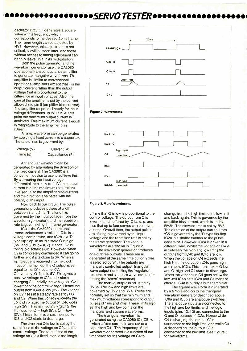
)sERVO TESTER1oscillator circuit. It generates a squarewave with a frequency whichcorresponds to the desired 20ms frame.The frame length can be adjusted byRV1. However, this adjustment is notcritical, as will be seen later, and thosewithout access to timing equipment canhappily leave RV1 in its mid -position.
Both the pulse generator and thewaveform generator use the CA3080operational transconductance amplifierto generate triangular waveforms. Thisamplifier is similar to conventionaloperational amplifiers except that it is theoutput current rather than the outputvoltage that is proportional to thedifference in input voltages. Also, thegain of the amplifier is set by the currentallowed into pin 5 (amplifier bias current).The amplifier responds linearly for inputvoltage differences up to 0.1V. At thispoint the maximum output current isachieved. This maximum current is equalin magnitude to the amplifier biascurrent.
A ramp waveform can be generatedby applying a fixed current to a capacitor.The rate of rise is governed by:
Voltage (V) Current (A)
Time (s) - Capacitance (F)
A triangular waveform can begenerated by alternating the direction ofthe fixed current. The CA3080 is aconvenient device to use to achieve this.By alternating the input voltagedifferential from +1V to =1V, the outputcurrent is at the maximum (saturation)level (equal to the amplifier bias current)and the direction alternates with thepolarity of the input.
Now back to our circuit. The pulsegenerator produces pulses of widthbetween 1 and 2ms. The length isgoverned by the input voltage (from thewaveform generator), and the repetitionrate is governed by the frame generator.
IC3 is the CA3080 operationaltransconductance amplifier. IC4d is avoltage comparator, and IC2b is a 'D'type flip -Bpi). In its idle state Q is high(5V) and Q is low (OV). Hence IC3 istrying to discharge C2. However, whenC2 is completely discharged it can go nofurther and it sits close to OV. When arising edge is received into the clockinput of the flip-flop, the Q output is setequal to the input, i.e. OV.Conversely, Q flips to 5V. This gives apositive voltage to IC3 and it startscharging C2. Initially the voltage on C2 islower than the control voltage. Hence theoutput from IC4d is low (OV). The voltageon C2 rises at a steady rate set by R3and C2. When this voltage exceeds thecontrol voltage, the output of IC4d goeshigh (5V). This immediately SETS' theflip-flop, i.e. Q = high (5V), Q = low(OV). This in turn reverses the input toIC3 and C2 starts to discharge.
The time that Q is low is set by therate of rise of the voltage on C2 and thecontrol voltage. The rate of rise of thevoltage on C2 is fixed. Hence the length
h--FRAMEIIC1c1_1
IC2b 0
IC2b
VCONTROL
C2
IC4d
toms
Figure 2. Waveforms.
IC2a
IC2a
C4
IC4c
IC4b
high limit
low limit
high limit
IC6a,b low limit
I I I
Figure 3. More Waveforms.
of time that Q is low is proportional to thecontrol voltage. The output from Q isinverted and buffered by IC1a, d, e, andf, so that up to four servos can be drivenat once. Overall then, the output pulsesare of length governed by the inputvoltage and the repetition rate is set bythe frame generator. The variouswaveforms are shown in Figure 2.
The waveform generator producesone of three outputs. These are allgenerated at the same time but only oneis selected by S1. The outputs are:manually controlled output, triangularwave output (for testing the 'regulator'response) and a square wave output (fortesting the 'servo' response).
The manual output is adjusted byRV3a. The low and high limits aregoverned by RV2 and RV4. These arenormally set so that the minimum andmaximum voltages correspond to outputpulses of 1 ms and 2ms. These limits alsoset the high and low points on thetriangular and square waveforms.
The triangular waveform isgenerated using the CA3080 IC (IC5) toswitch a fixed current in and out of acapacitor (C4). The frequency of thewaveform generated is a function of thetime taken for the voltage on C4 to
change from the high limit to the low limitanc back again. This is governed by theamplifier bias current, which is set byRV3b. The slowest time is set by RV5.The direction of the output current fromIC5 is governed by the 'D' type flip-flopIC2a in a similar manner to the pulsegenerator. However, IC2a is driven in adifferent way. Whilst the voltage on C4 isin between the high and low limits theoutputs from IC4b and IC4c are low.When the voltage on C4 exceeds thehigh limit the output on IC4c goes highanc resets IC2a. This then makes Q lowanc Q high and C4 starts to discharge.When the voltage on C4 goes below thelow limit IC4b sets IC2a and C4 starts tocharge. IC4a is purely a buffer amplifier.
The square waveform is generatedby a simple add-on to the triangularwaveform generator described above.IC6a and IC6b are analogue switches.The analogue inputs are connected tothe high and low limits, and the logicinputs (pns 12, 13) are connected to theQ and Q outputs of IC2a. Hence whileC4 s charging, the output 'C' isconnected to the high limit, and while C4is discharging, the output C' isconnected to the low limit. See Figure 3for waveforms.
17
4.mosERVO TESTER..........4Construction
This is straightforward. Refer toFigure 4 for the pcb layout and legend.Some care should be taken to avoidstatic charges when handling the CMOSIC's. Try to fit these last if possible, andalways fit them after the power supplysmoothing capacitors (C5 and C6) havebeen installed. Solder the power rail pinsfirst (pins 7 and 14). Otherwise solder atwill! A good plan is to do resistors first,then capacitors then the three wire links,using cut off resistor leads, and lastly theIC's. It is not necessary to connect all the4 outputs. These can be connected inparallel if extra power is needed. Whenconnecting the output sockets make surethat the correct wire goes to each pin.Also take care when testing differentservos. There are some manufacturerswho use the same sockets but differentpin conventions.
Figure 5 shows box cut-out details.Mount the completed board into the boxusing M3 fixings as shown in Figure 6.Cut the shaft of RV3 to approximately12mm, and fit a knob. The tang of S1should also protrude through the slot cutin the side of the box. Fit the lid with thepower wires and output connectionsprotruding through the notches. Tofinish, stick on the front panel.
Set-up and TestingThe Servo Tester was designed to
be powered by a 4.8V standard radiocontrol battery pack. Alternatively, a 5V1 A power supply could be used.
Start by positioning all thepotentiometers in their mid -positions,and setting the selector switch S1 tomanual. Connect the battery powersupply. If an oscilloscope is available,the frame can be set to 20ms byadjusting RV1. This is not critical. Someradio control systems have a variableframe. Here the frame is set by the sumof the pulse widths of all the channelsplus the 'sync' pulse, which is usuallyabout 8ms long. Hence on a sevenchannel system the frame can vary from15ms to 22ms.
Next set the high and low limits(RV2 and RV4). A good starting point isto adjust these so that the ends of RV3aare at 1.8V and 2.8V. Final setting canthen be performed using an oscilloscopeor by using a servo on which the outputarm movement range has been notedfrom its use on another radio controlsystem. Adjust RV2 to give 2ms withRV3 fully clockwise and RV4 to give 1 mswith RV3 fully anticlockwise. There issome interaction between these settingsso it will be necessary to alternatelyadjust RV2 and RV4 several times.
Now connect a servo (if you havenot done so already). Movement of RV3should give a corresponding movementin the servo. Set S1 to triangular wave.The servo arm should now be movingfrom one extreme to the other at a ratedetermined by RV3. With RV3 in the fullyanticlockwise position, adjust RV5 to
E ICh
-1-
tt
IC2
-1-IC5
11
+veov
RV1
1C3
R1
(+)3Liir::4
Figure 4. Pcb layout and circuit references.
3 pitches 014.12Notch 2 wide x 2deep,4posns
905
Hole 010 -
41.
45
Slot 140 6
29
Note Lid lip to be notched 2 wide x 2 deepcorresponding with notches in box. Alldimensions in mm.
Figure 5. Box drilling.
0
0.0
0.
LK +v
-1-
5
give the slowest desired transit time. Atime of about 50 seconds isrecommended.
Use of the Servo Tester1. Servo Travel
Use the manual control to set theservo from one extreme to the other.Then with a protractor measure theservo travel. Typical values are 70° -90° for regular servos or 180° for'retract' servos.
2. Servo Resolution (or Sensitivity)Set the selector switch (S1) to the
mid -position (triangular wave) and set
12mm
/M3 Clearance spacerM3 x10 Csk screw, nut& washer
Figure 6. Mounting pcb in box.
18
SERVO TESTER.RV3 fully anticlockwise. As the pulseslowly changes the servo will respondin small jumps. The servo traveldivided by the number of jumps willgive the resolution (typically 0.5°). Ifthe slowest transit time has been setto 50 seconds it will only benecessary to count the jumps over 10seconds and multiply by 5. This test isalso useful for showing up anyproblems with the servo feedbackpotentiometer.
3. Servo Transit TimeStart with S1 in the squarewave
position and RV3 fully anticlockwise.The servo will now switch from oneextreme to the other every 50seconds. Slowly turn RV3 clockwisewhile listening carefully for the gaps inthe servo movements. When thesedisappear the servo is moving at itsmaximum speed. Measure the timefor 20 swings and divide by 20 to getthe transit time, (typically 0.3 to 0.5seconds). This can be divided by theservo travel to give the servo speed interms of seconds per degree.
4. OvershootWith S1 in the squarewave position
and RV3 set to get the servo to movefull travel about once per second, usea protractor above the servo arm tomeasure the overshoot, (typicalvalues 0 - 5°).
5. Compare Two ServosPlug both servos into the tester and
run through all the tests. Theadvantage of doing two at once is thatone can get a feel for theirdifferences.
One last thought. Before desc-ending on your local model shop to testhis servos, make absolutely certain thatyour tester is working correctly on eachof the outputs, and, of course, that thepin conventions that you have used onyour sockets correspond to the pinconventions of the servos being tested.
SERVO TESTERPARTS LIST
IC4 LM324 1 (UF26D)IC6 4066BE 1 (QX23A)
MISCELLANEOUSRESISTORS: All 0.6W 1% Metal Film (Unless specified) SI R/A DT3T Slide 1 (FVO2C)R1 56k 1 (M56K) PCB 1 (GD41U)R2 220k 1 (M220K) Knob K14 A 1 (FK38R)R3 47k 1 (M47K) ABS Box MB2 1 (LH21X)R4,5,7,8,10 22k 5 (M22K) Spacer M3 x L'e in. 1 Pkt (FG32K)R6,9 10k 2 (M1OK) Pozi Screw M3 x 10m 1 Pkt (LR57M)RV1 47k Hor End Preset 1 (UHO5F) Isowasher M3 1 Pkt (BF62S)RV2 22k Hor End Preset 1 (UH04E) Isonut M3 1 Pkt (BF58N)RV3 4k7 Dual Pot Lin 1 (FW84F) Wire 7/0.2 lOrn Black 1 Pkt (BLOOA)RV4 10k Hor End Preset 1 (1.11:03D) Wire 7/0.2 10m Red 1 Pkt (BLO7H)RV5 lk Hor End Preset 1 (UHOOA) Wire 7/0.2 10m White 1 Pkt (BLO9K)
Front Panel 1 (FP75S)CAPACITORS Instruction Leaflet 1 (XT78K)C1 100nF Poly Layer 1 (WW41U) Constructors' Guide 1 (XH79L)C2 68nF Poly Layer 1 (WW39N)C3,4 33p.F 101/ Tant 2 (WW74R)C5 1000pF 10V Axial 1 (FB81C) The above items are available as a kit:C6 100nF Mylar 1 (WW21X) Order As LM23A (Servo Tester Kit).
SEMICONDUCTORSThe following items (which are included in the kit) are also
available separately.IC1 4069UBE 1 (QX25C) PCB Order As GD41U.IC2 4013BE 1 (QX07H) Front Panel Order As FP75S.IC3,5 CA3080E 2 (YH58N)
19

Weather SatelliteDown Converter
by Robert Kirsch Part 2
This is the second article describinga Down Converter for use with theMAPSAT VHF Receiver and Decoder.The previous article covered theMeteosat System with a technical desc-ription of the Down Converter and Pre-amplifier, as well as the requirementsnecessary for the sighting of the aerialsystem. This article describes the instal-lation and testing of the complete systemand also the circuit description andconstruction details for the ChannelSwitching Unit.
Aerial andPre -amplifier
The aerial kit (LM22Y) is suppliedwith all metalwork pre -drilled and cut tolength, all necessary screws, nuts andwashers are also included together withfull assembly instructions. The ready -built and pre -aligned Pre -amplifier isalso included with this kit. Note: This kitdoes not include a mast or lashings, andsomething suitable should be chosen foryour particular installation, bearing inmind the sighting requirements des-cribed in the previous article. The systemshould, if possible, be tested at groundlevel before the aerial is installed in itsfinal position, see 'Pre -Installation Tests'below.
Down ConverterThis unit is ready -built and aligned
and requires no action at this stage otherthan roughly determining its final positionin order to find the approximate length offeeder that will be used, as this isrequired during testing.
Channel Switching UnitThis unit is required in order to
change the channel being received bythe Down Converter. The unit is con-nected in series with the aerial cable thatexits from the Down Converter, and thenconnects to the aerial socket of theMapsat Receiver.
When the Receiver and DownConverter are first powered up, channel1 is automatically selected. Channel 2 isselected by operating the toggle switch
Channel Switching Unit.
located on the front panel of the controlunit in the appropriate direction. Thiscauses a short break in the power supplywhich is detected by the channelswitching logic in the Down Converter,and switches the channel 2 crystal intocircuit. The toggle switch, when movedto the channel 1 position, causes a longerbreak in the supply to the DownConverter and the switching logic willnow select the channel 1 crystal.
Circuit DescriptionFigure 1 shows the circuit of the
Channel Switching Unit. Figure 5 of theDown Converter article includes thechannel switching logic and crystaloscillator circuits.
The radio frequency signals fromthe Down Converter enter the unit viaSK1 and are directly coupled to theReceiver via C6 and SK2. The supplyfrom the Receiver (positive on the coaxcentre conductor and negative on thescreen) is separated from the RF signalsby L2 which provides a high impedanceto the signals at 137.5MHz, but has a lowresistance to DC. This supply is con-nected via the contacts of RL1, LI and SK1to the Down Converter.
When the toggle switch is moved tochannel 2 position, the input of theinverter ICle is pulled high, the outputgoes low and the pulse caused by C8charging is inverted by ICU, turns on TR3and operates RL1 for a short period. Thecontacts of RL 1 are normally made andthus this pulse causes a short break in thesupply to the Down Converter. When theswitch is moved to the channel 1 positionthe same sequence of events occur but inthis case the pulse length is determinedby C7, this being a higher capacity, thepulse is longer and the supply isinterrupted for a greater period of time.
The circuit formed by IC la, b and cis used to mimic the channel switchinglogic in the Down Converter in order todrive the LEDs that show which channelhas been selected. The input to thiscircuit is via DI and C3, which areconnected to the switched side of theunit. When a short duration interruptionoccurs C3 produces a short positivegoing pulse at the point when the poweris restored, this causes the latch formedby IC la and c to change state. During thisprocess, Cl has remained charged andthe output of the inverter IC lb remainslow and has no effect on the latch. When
20
OUT TO
DOWN CONVERTER
5KI
BV
L.
1UH
C61ONF
DC IN FROM
MAP5AT RECEIVER
5K2
CLOSED WITH POWER OFF
RLI
C2
2N2FT
05
SZ 1N4
I148
RI
IM
C3ISONF
ICI
A
40106
02 7[164148
u m CI
1806F
I
51
R3108Kr--1
R4100K
R2 R52M IOW
0
-V
BV
L2 !!
IUH
II(
T81.4
101.2
0
9
II
40186
ICI
10
D31.3
6
ICI
40106
03164148
ICI
11B
40106
4C4 min
100NFoi
R6 R7 -
10K 10K__
40106
BC327
R810K
R910K
T 1
C5100NF
TRI
14f48
05164148
C7560NF
U
C8 07< 1N4148
BC327
RIO1KTR2 TB 1.6
0
LI
ICI PIN14 + VOLTS
ICI PIN7 OV
RED-
LO1
All RED
T81.I
L32
C9 c22UF.16V
OV
CIO -
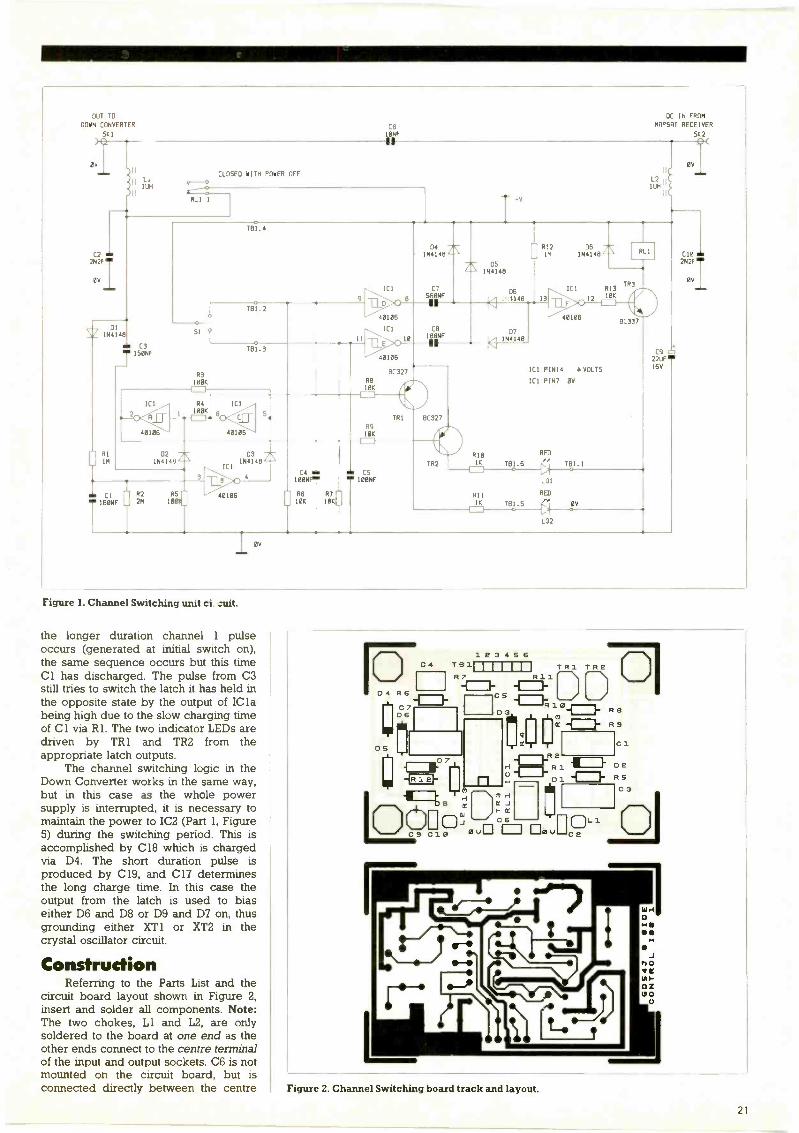
Figure 1. Channel Switching unit
the longer duration channel 1 pulseoccurs (generated at initial switch on),the same sequence occurs but this timeCl has discharged. The pulse from C3still tries to switch the latch it has held inthe opposite state by the output of IClabeing high due to the slow charging timeof Cl via R 1. The two indicator LEDs aredriven by TR1 and TR2 from theappropriate latch outputs.
The channel switching logic in theDown Converter works in the same way,but in this case as the whole powersupply is interrupted, it is necessary tomaintain the power to IC2 (Part 1, Figure5) during the switching period. This isaccomplished by C18 which is chargedvia D4. The short duration pulse isproduced by C19, and C17 determinesthe long charge time. In this case theoutput from the latch is used to biaseither D6 and D8 or D9 and D7 on, thusgrounding either XT1 or XT2 in thecrystal oscillator circuit.
ConstructionReferring to the Parts List and the
circuit board layout shown in Figure 2,insert and solder all components. Note:The two chokes, LI and L2, are onlysoldered to the board at one end as theother ends connect to the centre terminalof the input and output sockets. C6 is notmounted on the circuit board, but isconnected directly between the centre
123456T e 1 MM. TR1 TReR7 R11
C
R
[117 R EC
T
n15,4
CC _I
I- e
C 6 n o-= . vu
-11=a D e
o 1 -E73- RSC3
O
R1
P,o
r-4 0 0
Figure 2. Channel Switching board track and layout.
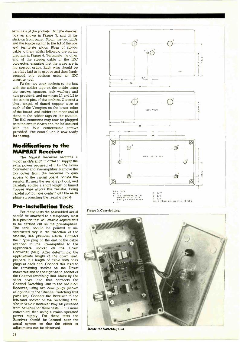
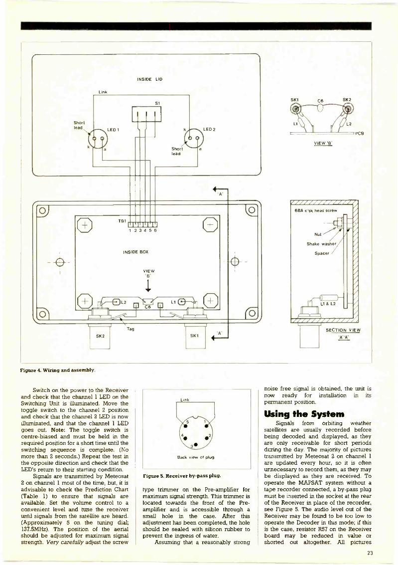
terminals of the sockets. Drill the die-castbox as shown in Figure 3, and fit thestick -on front panel. Mount the two LEDsand the toggle switch to the lid of the boxand terminate about 10cm of ribboncable to them whilst following the wiringdiagram in Figure 4. Terminate the otherend of the ribbon cable in the IDCconnector, ensuring that the wires are inthe correct order. Each wire should becarefully laid in its groove and then firmlypressed into position using an IDCinsertion tool.
Fit the two coax sockets to the boxwith the solder tags on the inside usingthe screws, spacers, lock washers andnuts provided, and terminate LI and L2 tothe centre pins of the sockets. Connect ashort length of tinned copper wire toeach of the Veropins on the lower edgeof the board, and solder the other end ofthese to the solder tags on the sockets.The IDC connector may now be pluggedonto the circuit board and the lid securedwith the four countersunk screwsprovided. The control unit is now readyfor testing.
Modifications to theMAPSAT Receiver
The Mapsat Receiver requires aminor modification in order to supply theextra power required of it by the DownConverter and Pre -amplifier. Remove thetop cover from the Receiver to gainaccess to the circuit board. Locate theresistor RI near the aerial input coil, andcarefully solder a short length of tinnedcopper wire across this resistor, beingcareful not to make contact with the earthplane surrounding the resistor pads!
Pre -Installation TestsFor these tests the assembled aerial
should be attached to a temporary mastin a position that will enable adjustmentsto be carried out on the pre -amplifier.The aerial should be pointed at un-obstructed sky in the direction of thesatellite, see previous article. Connectthe F type plug on the end of the cableattached to the Pre -amplifier to theappropriate socket on the DownConverter (SKI). After determining theapproximate length of the down lead,prepare this length of cable with coaxplugs at each end. Connect this lead tothe remaining socket on the Downconverter and to the right-hand socket ofthe Channel Switching Unit. Make up theshort coax lead that connects theChannel Switching Unit to the MAPSATReceiver, using two coax plugs (shownas optional in the Channel Switching Unitparts list). Connect the Receiver to theleft-hand socket of the Switching Unit.The MAPSAT Receiver may be poweredfrom batteries for these tests, if it is moreconvenient than using a mains operatedpower supply. For these tests theReceiver should be located near theaerial system so that the effect ofadjustments can be observed.
6.435 H
- 70 --
- 65-
SITE VIEW
35
I- -T- 85-
66 -
92 -
VIEW INSIDE BOX
(9) (Q)
(6
HOLE ORTRA 2.4B 3.2 COUNTERSINK ON
UNDERSIDE TO SUIT6BA C.SK HEAD SCREW
C 4
D 6.75
E 9.5F 6.2ALL DIMENSIONS IN MILLIMETRES
A
,;
N
RU
0
-A
Figure 3. Case drilling.
Inside the Switching Unit.
22
Shortlead
INSIDE LID
Link
LED 1
Si
Shortlead
TB1 II III1 2 3 4 5 6
INSIDE BOX
VIEW
C6 0
Tag
SK2
Figure 4. Wiring and assembly.
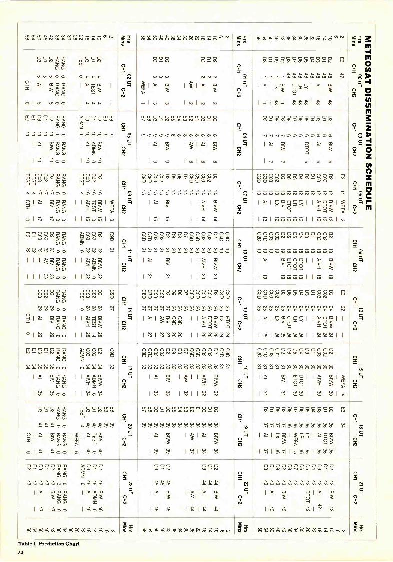
Switch on the power to the Receiverand check that the channel 1 LED on theSwitching Unit is illuminated. Move thetoggle switch to the channel 2 positionand check that the channel 2 LED is nowilluminated, and that the channel 1 LEDgoes out. Note: The toggle switch iscentre -biased and must be held in therequired position for a short time until theswitching sequence is complete. (Nomore than 2 seconds.) Repeat the test inthe opposite direction and check that theLED's return to their starting condition.
Signals are transmitted by Meteosat2 on channel 1 most of the time, but, it isadvisable to check the Prediction Chart(Table 1) to ensure that signals areavailable. Set the volume control to aconvenient level and tune the receiveruntil signals from the satellite are heard.(Approximately 5 on the tuning dial;137.5MHz). The position of the aerialshould be adjusted for maximum signalstrength. Very carefully adjust the screw
SK1
Link
Back view of plug
Figure 5. Receiver by-pass plug.
type trimmer on the Pre -amplifier formaximum signal strength. This trimmer islocated towards the front of the Pre-amplifier and is accessible through asmall hole in the case. After thisadjustment has been completed, the holeshould be sealed with silicon rubber toprevent the ingress of water.
Assuming that a reasonably strong
SK1 C6
VIEW 'B'
SK2
PCB
(//////////////6BA c'sk head screw //
Nut /.../ %
Shake washer /
Spacer ////
- /---(/Fri2L1 d
/:,7.7/7)///7///,
SECTION VIEW
noise free signal is obtained, the unit isnow ready for installation in itspermanent position.
Using the SystemSignals from orbiting weather
satellites are usually recorded beforebeing decoded and displayed, as theyare only receivable for short periodsduring the day. The majority of picturestransmitted by Meteosat 2 on channel 1are updated every hour, so it is oftenurnecessary to record them, as they maybe displayed as they are received. Tooperate the MAPSAT system without atape recorder connected, a by-pass plugmast be inserted in the socket at the rearof the Receiver in place of the recorder,see Figure 5. The audio level out of theReceiver may be found to be too low tooperate the Decoder in this mode; if thisis the case, resistor R57 on the Receiverboard may be reduced in value orshorted out altogether. All pictures
23
ME
TE
OS
AT
DIS
SE
MIN
AT
ION
SC
HE
DU
LEH
rsM
insC
H1
00 UT
CH
2C
H1
03 UT
CH
2C
H1
06 UT
CH
2C
H1
09 UT
CH
2C
H1
12 UT
CH
2C
H1
15 UT
CH
2C
H1
1U ui
CH
2C
H1
z1 u IC
H2
rueM
ins
2E
347
E3
11W
EF
A2
E3
22 -W
EF
A4
E3
342
6-
--
--
-6
10D
248
BIW
48D
26
BIW
6D
212
BIV
W12
B2
18B
IVW
18D
224
BIV
W24
D2
30B
IVW
30D
236
BIV
W36
D2
42B
IW42
10
14D
148
D1
6C
O2
12D
TO
T12
CO
218
CO
224
DT
OT
24C
O2
30D
136
DT
OT
36D
142
14
18D
348
Al
48D
36
Al
6C
O3
12A
IVH
12C
O3
18A
IVH
18C
O3
24A
IVH
24C
O3
30A
IVH
30D
336
AI
36D
342
Al
4218
22D
448 -
-D
46 -
-D
112
--
D1
18-
-D
124 -
-D
130
--
D4
36 --
D4
42 --
22
26D
548
LY48
D5
6D
TO
T6
D3
12-
-D
318
--
D3
24 --
D3
30-
-D
536
LY36
D5
42D
TO
T 42
26
30D
648
LR48
D6
6D
412
LY12
D4
18D
TO
T18
D4
24LY
24D
430
DT
OT
30D
636
LR36
D6
4230
34D
748
DT
OT
48D
76
D5
12LR
12D
518
CT
OT
18D
524
LR24
D5
30E
TO
T 30
D7
36W
EF
A5
D7
4234
38D
848
D8
6D
612
ET
OT
12D
618
ET
OT
18D
624
CT
OT
24D
630
D8
36 --
D8
4238
42D
21
BIW
1D
27
BIW
7D
213
BIV
13D
219
BIV
19D
225
BIV
25D
231
BIV
31D
237
BIV
W37
D2
43B
IW43
42
46D
91
LX48
D9
7C
O2
13LX
12C
O2
19C
O2
25LX
24C
O2
31D
937
LX36
D9
4346
50D
11 -
-D
17
Al
7C
O3
13-
-C
O3
19C
O3
25 --
CO
331
D1
37 --
D1
43A
l43
50
54D
31
Al
1D
37 -
C3D
13A
l13
C1D
19A
l19
C1D
25A
l25
C1D
31A
l31
D3
37A
l37
D3
43-
-54
58-
C2D
13-
-C
2D19
--
C2D
25 --
C2D
31-
--
-58
Hrs
01 UT
04 UT
07 UT
10 UT
13 UT
16 UT
19 UT
22 UT
Hrs
Mins
CH
1C
H2
CH
1C
H2
CH
1C
H2
CH
1C
H2
CH
1C
H2
CH
1C
H2
CH
1C
H2
CH
1C
H2
Mins
2C
3D19
C3D
25E
TO
T24
C3D
312
6C
4D19
C4D
25L2
24C
4D31
6
10D
22
BIW
2D
28
BIW
8D
214
BIV
W14
D2
20B
IVW
20D
226
BIV
W26
D2
32B
IVW
32D
238
BIV
W38
D2
44B
IW44
10
14D
12
D1
8C
O2
14C
O2
20C
O2
26D
TO
T 26
CO
232
D1
38D
144
14
18D
32
Al
2D
38
Al
8C
O3
14A
IVH
14C
O3
20A
IVH
20C
O3
26A
IVH
26C
O3
32A
IVH
32D
338
Al
38D
344
Al
4418
22-
-E
l8 -
-C
5D14 -
-C
5D20
--
C5D
26 --
C5D
32-
-E
l38 -
--
-22
26A
W2
E2
8A
W8
C6D
14-
-C
6D20
-C
6D26 -
C6D
32 --
E2
38A
W37
AW
4426
30-
E3
8 -D
714
D7
20D
726
D7
32A
W32
E3
38 --
--
30
34E
48
0814
D8
20D
826
C8D
26D
832 -
-E
438
34
38E
58
D9
14D
920
D9
26C
9D26
D9
32E
538
38
42D
23
81W3
D2
9B
IW9
D2
15B
IV15
D2
21B
IV21
D2
27B
IV27
D2
33B
IV33
D2
39B
IVW
39D
245
BIW
4542
46D
13
D1
9C
O2
15C
O2
21C
O2
27 AW
27C
O2
33D
139
D1
4546
50D
33
Al
3D
39
Al
9C
O3
15A
l15
CO
321
CO
327 -
-C
O3
33A
l33
D3
39A
l39
D3
45A
l45
50
54-
-E
69 -
C8D
15-
-C
7D21
Al
21C
7D27
Al
27C
7D33
--
E6
39 --
--
54
58W
EF
A1
E7
9C
9D15
C8D
21-
-C
8D27 -
-C
8D33
E7
3958
Hrs
02 UT
05 UT
08 UT
11 UT
14 UT
17 UT
20 UT
23 UT
Hrs
Mins
CH
1C
H2
CH
1C
H2
CH
1C
H2
CH
1C
H2
CH
1C
H2
CH
1C
H2
CH
1C
H2
CH
1C
H2
Mins
2-
E8
9W
EF
A3
C9D
21C
9D27
C9D
33E
839
2
6E
99
--
E9
396
10D
24
BIW
4D
210
BIW
10D
216
BIV
W16
D2
22B
IVW
22D
228
BIV
W28
D2
34B
IVW
34D
240
BlV
d40
D2
46B
IW46
10
14D
14
TE
ST
4D
110
AD
MN
0C
O2
16T
ES
T0
CO
222
AD
MN
0C
O2
28T
ES
T4
CO
234
AD
MN
CD
140
TE
oT0
D1
46A
DM
N0
14
18D
34
Al
4D
310
Al
10C
O3
16A
IVH
16C
O3
22A
IVH
22C
O3
28A
IVH
28C
O3
34A
IVH
3403
40A
l40
D3
46A
l46
18
22T
ES
T0 -
AD
MN
0 --
TE
ST
4-
-A
DM
N0 -
-T
ES
T0 -
-A
DM
N0 -
-T
ES
T4 -
-A
DM
N0
--
22
26-
--
--
-W
EF
A6
26
30-
-30
34R
AN
G0
RA
NG
0R
AN
G0
RA
NG
0R
AN
G0
RA
NG
0R
AN
G0
RA
NG
0R
AN
G0
RA
NG
0R
AN
G0
RA
NG
0R
AN
G0
RA
NG
0R
AN
G0
RA
NG
034
38R
AN
G0
RA
NG
0R
AN
G0
RA
NG
0R
AN
G0
RA
NG
0R
AN
G0
RA
NG
0R
AN
G0
RA
NG
0R
AN
G0
RA
NG
0R
AN
G0
RA
NG
0R
AN
G0
RA
NG
038
42D
25
BIW
5D
211
BIW
11D
217
BIV
17D
223
BIV
23D
229
BIV
29D
235
BIV
35D
241
BIW
41D
247
BIW
4742
46D
15
DI
11C
O2
17C
O2
23A
V23
CO
229
D1
35D
141
D1
4746
50D
35
Al
5D
311
Al
11C
O3
17A
l17
CO
323 -
-C
O3
29A
l29
D3
35A
l35
D3
41A
l41
D3
47A
l47
50
54-
-E
l11 -
-T
ES
T4 -
-E
l22 -
--
El
34 --
--
El
47 --
54
58C
TH
0E
211
TE
ST
4C
TH
0E
222 -
CT
H0
E2
34C
TH
0E
247
58

C5 C6 C7 C8 N9 ';
C10 C11 C12 C13 C14
C C16 C17 18
0tT9
20 C21 C22 23 C2
Figure 6. WEFAX visible formats.
transmitted by Meteosat are precededby a 5 second burst of peak white signal,the Input Level control on the Decodershould be adjusted to give a full scalereading on the level meter during thistone.
Types of PicturesMeteosat transmits the following
three types of picture:
1. Visible (C format).2. Infra -red (D format).3. Water vapour (E format).
All pictures include date, time andformat information and by using the mapsshown in Figures 6 and 7, as well asTable 1, it is possible to identify the areaof the Earth covered by the picture beingreceived. Thus the visible image thatcovers the largest area of the British Islesis labelled CO2. (An infra -red picture ofthe same area would be labelled C2D).
Channel 1 also transmits test pic-tures and administrative (ADMN) inform -
D1
El13
.1. ..11---
D2
E2
D4
E4
05
E5
Dtl
E6
D7 D8
E8
D9
Figure 7. WEFAX IR (formats D) and WV (formats E).
ation. Channel 2 transmits pictures of thewhole of Earth's disk (TOT) and alsometeorological charts (WEFA).
Information about Meteosat andNOAA satellites may be obtained bycalling UK Weatherwatch on 0256 83448,between 1715 and 0845, Monday toFriday or all day Saturday and Sunday.
Final InstallationThe aerial may be attached per-
manently to a standard television aeriallashing kit in a convenient position thatenables the sighting requirements to bemet, but bear in mind that for the finalpositioning it is best to adjust the aerialdirection and angle whilst monitoring thesignal strength on the Receiver.
The Down Converter may be mount-ed up to 4 metres from the aerial; thiscould enable it to be located inside abuilding but if this is not possible the unitshould be installed in a weather-proofbox (YM92A). Cable entry should be atthe bottom of the box and any gaps
around the cables sealed with siliconrubber (YJ91Y). Avoid locations wherethe Down Converter may get too hot andmount it in a shady position if possible.
The down lead from the DownConverter to the Receiver should be keptas short as possible to minimise signallosses, although the system has beenfound to work well with feeders of 15metres and over. Avoid running thedown lead close to sources of electricalinterference such as computers, printers,disk drives or video monitors. Longerdown leads may be used by inserting aninline 137.5MHz amplifier close to theDown Converter. This extra unit will alsohelp where high levels of interference (atVHF) cannot be avoided. (Details nextissue.)
As a matter of routine, a regularcheck should be made on all externalunits and the aerial elements should becleaned from time to time, taking carenot to damage the protective varnishapplied during construction.
Aerial Pre -amplifier. Down Converter mounted on a wall.
25

CHANNEL SWITCHING UNITPARTS LISTRESISTORS: All 0.6W 1% Metal Film
SI Sub -Min Toggle D 1 (FHO3D)TB1 PCB Latch P16 -way 1 (YW12N)
PCB Latch Hsng 6 -way 1 (BH65V)PCB Terminal 1 Pkt (YW25C)LED Clip 5mm 2 (YY40T)
R1,12 1M 2 (M1M) Box DCM5004 1 (LH71N)R2 2M2 1 (M2M2) PCB 1 (GD54J)R3,4,5 100k 3 (M100K) Front Panel 1 (FP76H)R6-9,13 10k 5 (M1OK) C/S Screw 6BA x 1/2 in. 1 Pkt (BF12N)R10,11 lk 2 (M1K) Shakeproof 6BA 1 Pict (BF26D)
Nut 6BA 1 Pkt (BF18U)CAPACITORS Spacer 6BA x Ve in. 1 Pkt (FW33L)C1,8 180nF Poly Layer 2 (WW44X) Ribbon Cable 10 -way lm (XR06G)C2,10 2n2F Monores Cap 2 (RA40T) Pin 2145 1 Pkt (FL24B)C3 150nF Poly Layer 1 (WW43W) Instruction Leaflet 1 (XT79L)C4,5 10011F 16V Minidisc 2 (YR75S) Constructors' Guide 1 (XH79L)C6 lOnF 50V Disc 1 (BX00A)C7 560nF Poly Layer 1 (WW50E) OPTIONAL (Not in Kit)C9 22pr 25V PC Elect 1 (FF06G) HQ Coax Plug 2 (FD85G)
Low -Loss Coax White As Reg (XR87U)SEMICONDUCTORSICI 40106BE 1 (QW64U)TR1,2 BC327 2 (QB66W)TR3 BC337 1 (QB68Y)D1-8 1N4148 8 (QL80B) The above items (excluding Optional) are available as a kit:
Order As LM26D (Channel Switch Unit).MISCELLANEOUS The following item (which is included in the kit) is alsoL1,2 Choke 1mH 2 (WH47B) available separately.LED1,2 LED Red 2 (WL27E) PCB Order As GD54J.SKI HQ Co -ax Socket 2 (FEIOL)RL I Micro -Min Relay 12V 1 (BK47B)
26
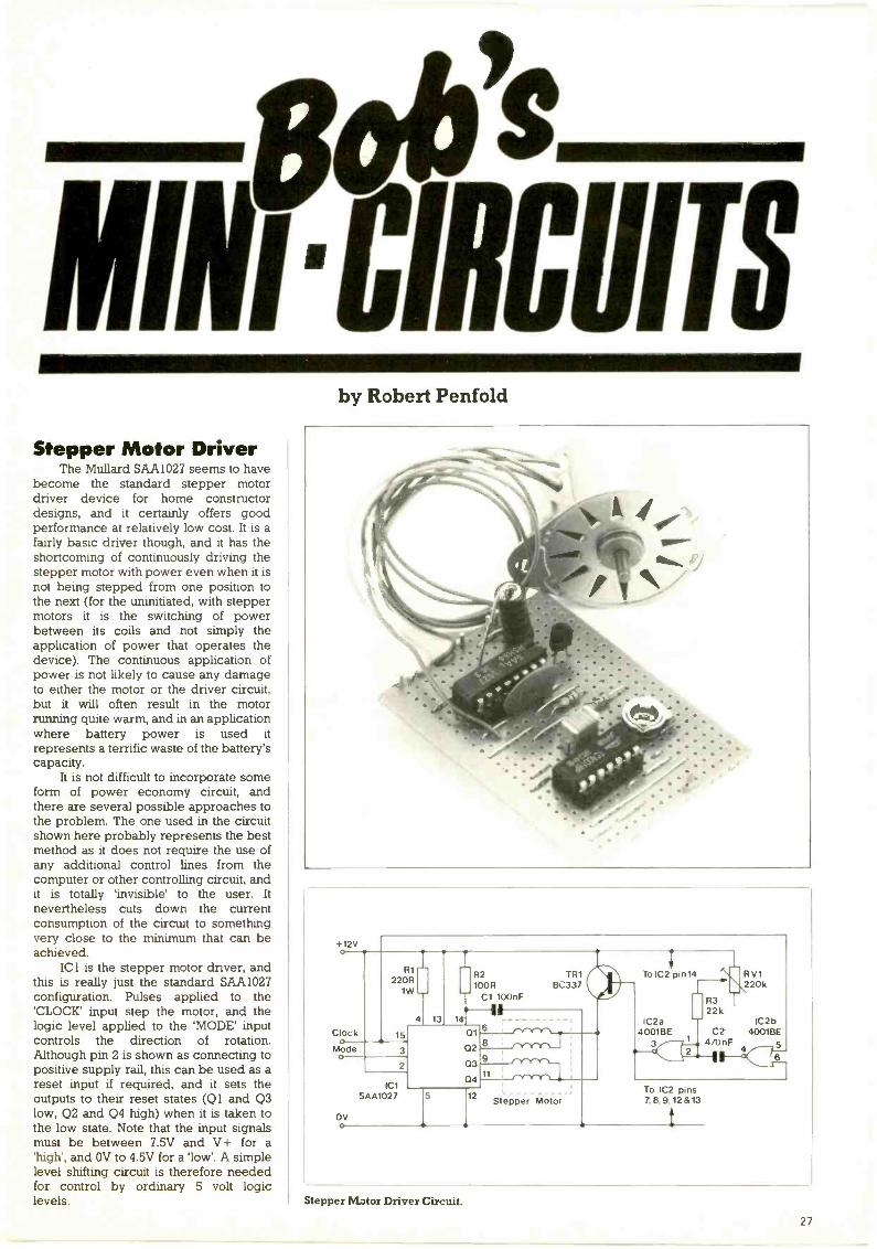
sob'sCIRCUITS
Stepper Motor DriverThe Mullard SAA1027 seems to have
become the standard stepper motordriver device for home constructordesigns, and it certainly offers goodperformance at relatively low cost. It is afairly basic driver though, and it has theshortcoming of continuously driving thestepper motor with power even when it isnot being stepped from one position tothe next (for the uninitiated, with steppermotors it is the switching of powerbetween its coils and not simply theapplication of power that operates thedevice). The continuous application ofpower is not likely to cause any damageto either the motor or the driver circuit,but it will often result in the motorrunning quite warm, and in an applicationwhere battery power is used it
represents a terrific waste of the battery'scapacity.
It is not difficult to incorporate someform of power economy circuit, andthere are several possible approaches tothe problem. The one used in the circuitshown here probably represents the bestmethod as it does not require the use ofany additional control lines from thecomputer or other controlling circuit, andit is totally 'invisible' to the user. It
nevertheless cuts down the currentconsumption of the circuit to somethingvery close to the minimum that can beachieved.
IC1 is the stepper motor driver, andthis is really just the standard SAA1027configuration. Pulses applied to the'CLOCK' input step the motor, and thelogic level applied to the 'MODE' inputcontrols the direction of rotation.Although pin 2 is shown as connecting topositive supply rail, this can be used as areset input if required, and it sets theoutputs to their reset states (Q1 and Q3low, 02 and Q4 high) when it is taken tothe low state. Note that the input signalsmust be between 7.5V and V+ for a'high', and OV to 4.5V for a 'low'. A simplelevel shifting circuit is therefore neededfor control by ordinary 5 volt logiclevels.
by Robert Penfold
+12V0
Clock0
Mode0
0 V0
RI220R
1W
15
3
2
'ClSAA1027
41 13 14
R2100R
Cl 10Onf
01
02
03
4
12 Stepper Motor
Stepper Mator Driver Circuit.
;To IC2 pin 14 i\R V1
220k
R3 T22k
IC2a40016E
3 1-2
IC2bBC2
1111-< 5_1-6-
To IC2 pins7.8,9,12813
27
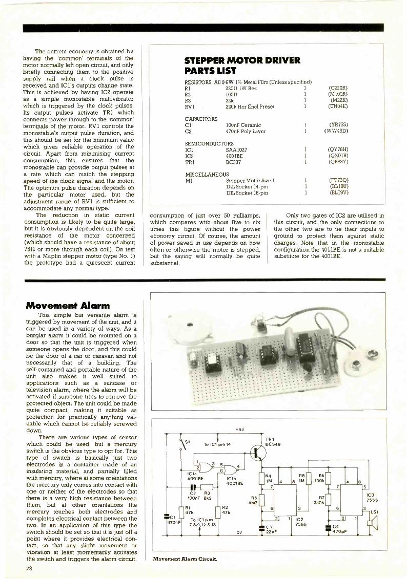
The current economy is obtained byhaving the 'common' terminals of themotor normally left open circuit, and onlybriefly connecting them to the positivesupply rail when a clock pulse isreceived and ICI's outputs change state.This is achieved by having IC2 operateas a simple monostable multivibratorwhich is triggered by the clock pulses.Its output pulses activate TR1 whichconnects power through to the 'common'terminals of the motor. RV1 controls themonostable's output pulse duration, andthis should be set for the minimum valuewhich gives reliable operation of thecircuit. Apart from minimising currentconsumption, this ensures that themonostable can provide output pulses ata rate which can match the steppingspeed of the clock signal and the motor.The optimum pulse duration depends onthe particular motor used, but theadjustment range of RV1 is sufficient toaccommodate any normal type.
The reduction in static currentconsumption is likely to be quite large,but it is obviously dependent on the coilresistance of the motor concerned(which should have a resistance of about7511 or more through each coil). On testwith a Maplin stepper motor (type No. 1)the prototype had a quiescent current
STEPPER MOTOR DRIVERPARTS LISTRESISTORS: All 0.6W 1% Metal Film (Unless specified)RI 22052 1W ResR2R3RV1
CAPACITORSClC2
10011
22k220k Hor End Preset
100nF Ceramic47011F Poly Layer
SEMICONDUCTORSICI SAA1027IC2 4001BETR1 BC337
MISCELLANEOUSM1 Stepper Motor Size 1
DIL Socket 14 -pinDIL Socket 16 -pin
consumption of just over 50 milliamps,which compares with about five to sixtimes this figure without the powereconomy circuit. Of course, the amountof power saved in use depends on howoften or otherwise the motor is stepped,but the saving will normally be quitesubstantial.
(C220R)(M100R)
(M22K)(UH04E)
1 (YR75S)1 (WW49D)
1 (QY76H)1 (QX018)1 (0868Y)
(FT73Q)(BL18U)(BL19V)
Only two gates of IC2 are utilised inthis circuit, and the only connections tothe other two are to tie their inputs toground to protect them against staticcharges. Note that in the monostableconfiguration the 4011BE is not a suitablesubstitute for the 4001BE.
Movement AlarmThis simple but versatile alarm is
triggered by movement of the unit, and itcan be used in a variety of ways. As aburglar alarm it could be mounted on adoor so that the unit is triggered whensomeone opens the door, and this couldbe the door of a car or caravan and notnecessarily that of a building. Theself-contained and portable nature of theunit also makes it well suited toapplications such as a suitcase ortelevision alarm, where the alarm will beactivated if someone tries to remove theprotected object. The unit could be madequite compact, making it suitable asprotection for practically anything val-uable which cannot be reliably screweddown.
There are various types of sensorwhich could be used, but a mercuryswitch is the obvious type to opt for. Thistype of switch is basically just twoelectrodes in a container made of aninsulating material, and partially filledwith mercury, where at some orientationsthe mercury only comes into contact withone or neither of the electrodes so thatthere is a very high resistance betweenthem, but at other orientations themercury touches both electrodes andcompletes electrical contact between thetwo. In an application of this type theswitch should be set so that it is just off apoint where it provides electrical con-tact, so that any slight movement orvibration at least momentarily activatesthe switch and triggers the alarm circuit.
+9V
S1 To IC1 pin 14TR1BC549
2 4
IC1b4001BE
R41M 4
R8
8 1MR6
100k
IC a4001BE
7 5
C2 R3100nF 8k2 R5
4M7R7
330k
IC37555
- R1 R2 347k 47k - LS1
noC1470nF To IC1 pins
7,8,9.12 1113
Movement Alarm Circuit.
OV
2I 1
C3T 22nF
IC27555 C4
T470pF
28
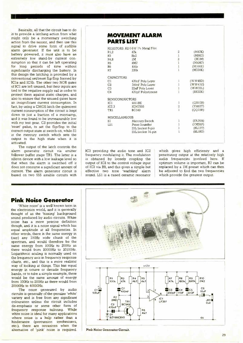
Basically, all that the circuit has to dois to provide a latching action from whatmight only be a momentary switchingaction from the sensor, and then use thissignal to drive some form of audiblealarm generator. If the unit is to bebattery powered, it must also have anextremely low stand-by current con-sumption so that it can be left operatingfor long periods of time withoutsignificantly discharging the battery. Inthis design the latching is provided by aconventional set/reset flip/flop formed byIC la and IC lb. The other two NOR gatesof IC1 are left unused, but their inputs aretied to the negative supply rail in order toprotect them against static charges, andalso to ensure that the unused gates havean insignificant current consumption. Infact, by using a CMOS latch the quiescentcurrent consumption of the circuit is keptdown to just a fraction of a microamp,and it was found to be immeasurably lowwith my test gear. C2 provides the initial'reset' pulse, to set the flip/flop to thecorrect output state at switch -on, while Siis the mercury switch which sets theoutput to the high state when it isactivated.
The output of the latch controls thealarm generator circuit via emitterfollower buffer stage TR1. The latter is asilicon device with a low leakage level sothat when the alarm is switched off it
does not consume a significant amount ofcurrent. The alarm generator circuit isbased on two 555 astable circuits with
MOVEMENT ALARMPARTS LISTRESISTORS: All 0-6W 1% Metal FilmR1,2 47k 2 (M47K)R3 8k2 1 (M8K2)R4,8 1M 2 (M1M)R5 4M7 1 (M4M7)R6 100k 1 (M100K)R7 330k 1 (M330K)
CAPACITORSCl 470rF Poly Layer 1 (WW49D)C2 100nF Poly Layer 1 (WW41U)C3 22nF Poly Layer 1 (WW33L)C4 470pF Polystyrene 1 (BX32K)
SEMICONDUCTORSIC1 400 IBE 1 (QX01B)IC2,3 ICM7555 2 (YH63T)TR1 BC549 1 (QQ15R)
MISCELLANEOUSSi Mercury Switch 1 (FA76H)LS1 Piezo Sounder 1 (FM59P)
DIL Socket 8 -pin 1 (BL17T)DIL Socket 14 -pin 1 (BL18U)
IC3 providing the audio tone and IC2frequency modulating it. The modulationis obtained by loosely coupling theoutput of IC2 to the control voltage inputof IC3 via R8, and this gives a simple buteffective two tone 'warbling' alarmsound. LS1 is a cased ceramic resonator
which gives high efficiency and apenetrating output at the relatively highaudio frequencies involved here. Ifoptimum volume is important, R7 can bereplaced by a 1M preset which can thenbe adjusted to find the two frequencieswhich provide the greatest output.
Pink Noise Generator'White noise' is a well known term in
the electronics world, and it is generallythought of as the 'hissing' backgroundsound produced by audio circuits. Whitenoise has a more precise definitionthough, and it is a noise signal which hasequal amplitude at all frequencies. Inother words, there is the same energy in(say) any 100Hz wide chunk of thespectrum, and would therefore be thesame energy from 100Hz to 200Hz asthere would from 20000Hz to 20100Hz.Logarithmic scaling is normally used onthe frequency axis in frequency responsecharts, etc., and this is a more realisticway of looking at things. This has equalenergy in octave or decade frequencybands, or to take a simple example, therewould be the same amount of energyfrom 100Hz to 200Hz as there would from20000Hz to 40000Hz.
The noise generated by audiocircuits is generally of the genuine 'white'variety and is free from any significantcolouration unless the circuit includesde -emphasis or some other form offrequency response tailoring. Whilewhite noise is ideal for many applicationswhere noise is a help rather than ahinderance (percussion synthesisers,etc.), there are occasions when thealternative of 'pink' noise is required.
+12V
Cl Ns100uF
R1100k
R22M2
C2470nF
*AIM 01
BZY88C6V2
R347k
C7470nF
TR1BC549
R44k7
R54k7
R64 k 7
R747k
R8180k
R9820k
7C3 C4 C5390pF 1n5F 3n3F
LF351
R102 M2
C610uF
OV
JK1Out
Pink Noise Generator Circuit.
29
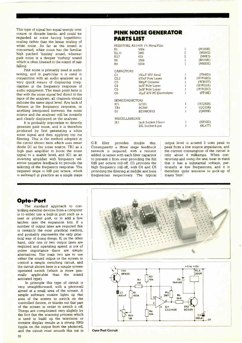
This type of signal has equal energy overoctave or decade bands, and could beregarded as noise having logarithmicscaling rather than the linear scaling ofwhite noise. As far as the sound isconcerned, white noise has the familiarhigh pitched 'hissing' sound, whereaspink noise is a deeper 'rushing' soundwhich is often likened to the sound of rainfalling.
Pink noise is primarily used in audiotesting, and in particular it is used inconjunction with an audio analyser as avery quick means of displaying irreg-ularities in the frequency response ofaudio equipment. The main point here isthat with the noise signal fed direct to theinput of the analyser, all channels shouldindicate the same input level. Any lack offlatness in the frequency response, oranything interposed between the noisesource and the analyser will be instantlyand clearly displayed on the analyser.
It is probably impossible to directlygenerate pink noise, and it is thereforeproduced by first generating a whitenoise signal and then applying top cutfiltering. This is the method adopted inthe circuit shown here which uses zenerdiode D1 as the noise source, TR1 as ahigh gain amplifier to boost the noisesignal to a usable level, and IC1 as aninverting amplifier with frequency sel-ective negative feedback to provide thetailoring of the frequency response. Therequired slope is 3dB per octave, whichis awkward in practice as a single stage
PINK NOISE GENERATORPARTS LISTRESISTORS: All 0.6W 1% Metal FilmRI 100k 1 (M100K)R2,10 2M2 2 (M2M2)R3,7 47k 2 (M4K7)R8 180k 1 (M180K)R9 820k 1 (M820K)
CAPACITORSC1 100µF 35V Axial 1 (FB49D)
C2,7 470nF Poly Layer 2 (WW49D)C3 390pF Ceramic 1 (WX63T)C4 1n5F Poly Layer 1 (WW23A)C5 3n3F Poly Layer 1 (WW25C)C6 10µF 50V PC Electrolytic 1 (FF04E)
SEMICONDUCTORSICI LF351 1 (WQ30H)TR1 BC549 1 (QQ15R)DI BZY88C6V2 1 (QH09K)
MISCELLANEOUSJK1 Jack Socket 3.5mm 1 (HF82D)
DIL Socket 8 -pin 1 (BL17T)
C -R filter provides double this.Consequently a three stage feedbacknetwork is required, with a resistoradded in series with each filter capacitorto prevent it from ever providing the full6dB per octave roll -off. C3 provides thehigh frequency roll -off, with C4 and C5providing the filtering at middle and bassfrequencies respectively. The typical
output level is around 2 volts peak topeak from a low source impedance, andthe current consumption of the circuit isonly about 4 milliamps. When con-structing and using the unit, bear in mindthat it has a substantial voltage, par-ticularly at low frequencies, and it istherefore quite sensitive to pick-up ofmains 'hum'.
Opto-PortThe standard approach to con-
trolling external devices from a computeris to either use a built-in port such as auser or printer port, or to add a fewlatches onto the expansion bus. If anumber of output lines are required thisis certainly the most practical method,and probably represents the only prac-tical way of doing things. If, on the otherhand, only one or two output lines arerequired and operating speed is not ofprime importance there are simplealternatives. The main two are to useeither the sound output or the screen tocontrol a simple switching circuit, andthe circuit shown here is a simple screenoperated switch (which is more gen-erally applicable than the soundactivated type).
In principle this type of circuit isvery straightforward, with a photocellaimed at a small area of the screen. Asimple software routine lights up thatarea of the screen to switch on thecontrolled device, or blanks out that partof the screen in order to switch it off.Things are complicated very slightly bythe fact that the scanning process whichis used to build up the television ormonitor display results in a strong 50Hzripple on the output from the photocell,and the circuit must smooth this out in
A
+5 to +12V
TR1BPX25
No Cl100nF
Tim
R21M
I 1
R310k D1
1N41487
RI R5100k 2M7 R6
7 -r 3k9
4 i
4 ICI TR2
R4CA3140E BC549
10k
T
Opto-Port Circuit.
RLA300R
C2100u71=1 ov
30
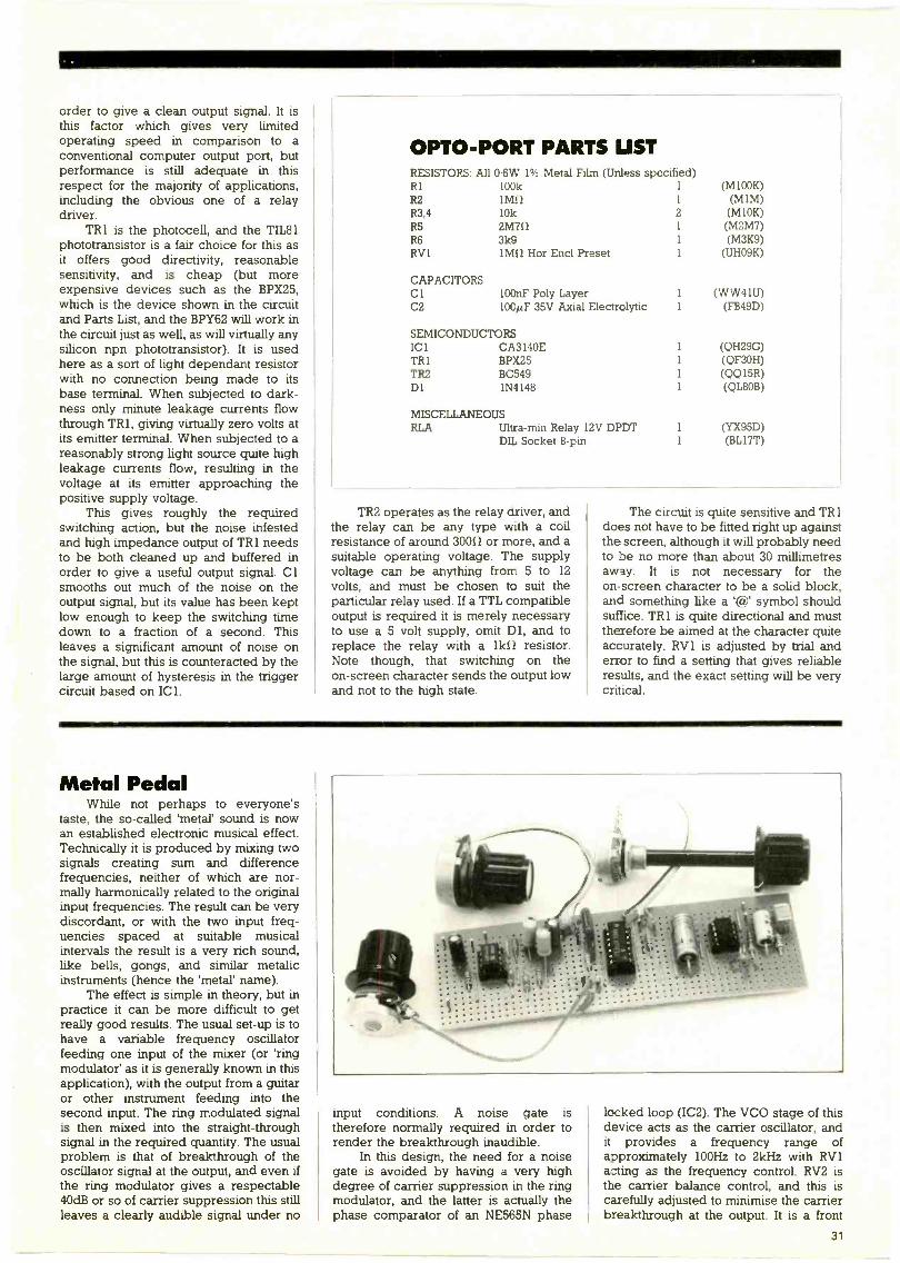
order to give a clean output signal. It isthis factor which gives very limitedoperating speed in comparison to aconventional computer output port, butperformance is still adequate in thisrespect for the majority of applications,including the obvious one of a relaydriver.
TR1 is the photocell, and the TIL81phototransistor is a fair choice for this asit offers good directivity, reasonablesensitivity, and is cheap (but moreexpensive devices such as the BPX25,which is the device shown in the circuitand Parts List, and the BPY62 will work inthe circuit just as well, as will virtually anysilicon npn phototransistor). It is usedhere as a sort of light dependant resistorwith no connection being made to itsbase terminal. When subjected to dark-ness only minute leakage currents flowthrough TR1, giving virtually zero volts atits emitter terminal. When subjected to areasonably strong light source quite highleakage currents flow, resulting in thevoltage at its emitter approaching thepositive supply voltage.
This gives roughly the requiredswitching action, but the noise infestedand high impedance output of TR 1 needsto be both cleaned up and buffered inorder to give a useful output signal. CIsmooths out much of the noise on theoutput signal, but its value has been keptlow enough to keep the switching timedown to a fraction of a second. Thisleaves a significant amount of noise onthe signal, but this is counteracted by thelarge amount of hysteresis in the triggercircuit based on IC 1.
OPTO-PORT PARTS USTRESISTORS: All 0.6W 1% Metal Film (Unless specified)RI 100k 1 (M 100K)R2 1 (M1M)R3,4 10k 2 (MIOK)RS 2M71) 1 (M2M7)R6 3k9 1 (M3K9)RV1 1MU Hor End Preset 1 (UHO9K)
CAPACITORSCl 100nF Poly Layer 1 (WW41U)C2 100µF 35V Axial Electrclytic 1 (FB49D)
SEMICONDUCTORSIC1 CA3140E 1 (QH29G)TR1 BPX25 1 (QF30H)TR2 BC549 1 (QQ15R)D1 1N4148 1 (QL80B)
MISCELLANEOUSRLA Ultra -min Relay 12V DPDT 1 (YX95D)
DIL Socket 8 -pin 1 (BL17T)
TR2 operates as the relay driver, andthe relay can be any type with a coilresistance of around 30012 or more, and asuitable operating voltage. The supplyvoltage can be anything from 5 to 12
volts, and must be chosen to suit theparticular relay used. If a TTL compatibleoutput is required it is merely necessaryto use a 5 volt supply, omit DI, and toreplace the relay with a lki/ resistor.Note though, that switching on theon -screen character sends the output lowand not to the high state.
The circuit is quite sensitive and TR1does not have to be fitted right up againstthe screen, although it will probably needto be no more than about 30 millimetresaway. It is not necessary for theon -screen character to be a solid block,and something like a '(a' symbol shouldsuffice. TR1 is quite directional and musttherefore be aimed at the character quiteaccurately. RV1 is adjusted by trial anderror to find a setting that gives reliableresults, and the exact setting will be verycritical.
Metal PedalWhile not perhaps to everyone's
taste, the so-called 'metal' sound is nowan established electronic musical effect.Technically it is produced by mixing twosignals creating sum and differencefrequencies, neither of which are nor-mally harmonically related to the originalinput frequencies. The result can be verydiscordant, or with the two input freq-uencies spaced at suitable musicalintervals the result is a very rich sound,like bells, gongs, and similar metalicinstruments (hence the 'metal' name).
The effect is simple in theory, but inpractice it can be more difficult to getreally good results. The usual set-up is tohave a variable frequency oscillatorfeeding one input of the mixer (or 'ringmodulator as it is generally known in thisapplication), with the output from a guitaror other instrument feeding into thesecond input. The ring modulated signalis then mixed into the straight -throughsignal in the required quantity. The usualproblem is that of breakthrough of theoscillator signal at the output, and even ifthe ring modulator gives a respectable40dB or so of carrier suppression this stillleaves a clearly audible signal under no
input conditions. A noise gate istherefore normally required in order torender the breakthrough inaudible.
In this design, the need for a noisegate is avoided by having a very highdegree of carrier suppression in the ringmodulator, and the latter is actually thephase comparator of an NE565N phase
locked loop (IC2). The VCO stage of thisdevice acts as the carrier oscillator, andit provides a frequency range ofapproximately 100Hz to 2kHz with RV1acting as the frequency control. RV2 isthe carrier balance control, and this iscarefully adjusted to minimise the carrierbreakthrough at the output. It is a front
31

+12V
Wet100uF
141
10k
R44 k 7
100kLin
R6100k
R3100k
I C3vill470nF
13
C2 R210uF 10k JK1
TIn
IC1741C
7
0
2
R55k6
1
IC2NE565N
C4T22nF
RV2 -47kLin
1=1051uF
RV3Log100k
R7100k
C6Tlu F
Re10k
-C710U F
Ft910k
Metal Pedal Circuit.
panel control rather than a preset, as theoptimum setting varies very slightly withchanges in the carrier frequency, andalthough a good compromise setting canbe found it was felt to be better to havethe ability to null out the carrier as muchas possible. The maximum degree ofcarrier suppression seems to be quitehigh, with around 80dB being achievable
with the prototype.ICI simply acts as an input buffer
stage which provides the unit with aninput impedance of about 100ki1. Itsoutput is direct coupled to the input ofIC2, for which it provides with thenecessary input bias voltage. IC3 acts asa conventional summing mode mixercircuit which combines the modulated
IC3
R10100k
+1:11-N,C8
10u FJK 2
741C Out
OV
and straight -through signals. RV3 con-trols the amount or ring modulated signalthat is mixed into the unprocessed signal.Signal levels of up to about 8 volts peak topeak can be handled using a 12 voltsupply (the use of a 9 volt battery supplyis not recommended). The current con-sumption is about 10 milliamps.
METAL PEDAL PARTS LIST C2,7,8 10µF 50V PC Electrolytic 3 (FF04E)C3 470nF Poly Layer 1 (WW49D)
RESISTORS: All 0-6W 1% Metal Film (Unless specified) C4 22nF Poly Layer 1 (WW33L)R1,2,8,9 10k 4 (MIOK) C5,6 1µF 100V PC Electrolytic 2 (FFO IB)R3,6,7,10 100k 4 (M100K)R4 4k7 1 (M4K7) SEMICONDUCTORSR5 5k6 1 (M5K6) IC1,3 µA741C (8 -pin DIL) 2 (QL22Y)RV1 100k LIN Pot 1 (FWO5F) IC2 NE565 1 (WQ56L)RV2 47k LIN Pot 1 (FW04E)RV3 100k LOG Pot 1 (FW25C) MISCELLANEOUS
JK1,2 Standard Jack Socket 2 (HF91Y)CAPACITORS DIL Socket 8 -pin 2 (BL17T)C1 100µF 35V Axial Electrolytic 1 (FB49D) DIL Socket 14 -pin 1 (BL 18U)
32


1
MEiMEN