Embed Size (px)
Citation preview

SERVICE MANUALMULTIFUNCTIONAL DIGITAL SYSTEMS
e-STUDIO163/203
File No. SME050024B0R05092196100-TTECVer02_2006-10
© July 2006 TOSHIBA TEC e-STUDIO163/203 CONTENTS
1
CONTENTS
1. SPECIFICATIONS / ACCESSORIES / OPTIONS / SUPPLIES ................................... 1-11.1 Specifications....................................................................................................................... 1-11.2 Accessories ......................................................................................................................... 1-41.3 Options ................................................................................................................................ 1-51.4 Supplies ............................................................................................................................... 1-61.5 System List .......................................................................................................................... 1-7
2. OUTLINE OF THE MACHINE ....................................................................................... 2-12.1 Sectional View ..................................................................................................................... 2-12.2 Electric Parts Layout............................................................................................................ 2-42.3 Symbols and Functions of Various Components............................................................... 2-112.4 General Description........................................................................................................... 2-15
2.4.1 System block diagram ............................................................................................ 2-152.4.2 Construction of boards ........................................................................................... 2-16
2.5 Disassembly and Replacement of Covers......................................................................... 2-182.6 Disassembly and Replacement of PC boards ................................................................... 2-232.7 Removal and Installation of Options.................................................................................. 2-28
3. COPY PROCESS .......................................................................................................... 3-13.1 General Description of Copying Process............................................................................. 3-13.2 Details of Copying Process.................................................................................................. 3-23.3 Comparison with e-STUDIO230/280 ................................................................................. 3-13
4. GENERAL OPERATION............................................................................................... 4-14.1 Overview of Operation ......................................................................................................... 4-14.2 Description of Operation...................................................................................................... 4-2
4.2.1 Warming-up.............................................................................................................. 4-24.2.2 Ready state (ready for copying) ............................................................................... 4-24.2.3 Drawer feed copying ................................................................................................ 4-34.2.4 Bypass feed copying ................................................................................................ 4-44.2.5 Interruption copying.................................................................................................. 4-4
4.3 Detection of Abnormality...................................................................................................... 4-54.3.1 Types of abnormality ................................................................................................ 4-54.3.2 Description of abnormality ........................................................................................ 4-6
4.4 Flow Chart ........................................................................................................................... 4-94.4.1 Immediately after the power is turned ON................................................................ 4-94.4.2 Automatic paper feed copying................................................................................ 4-11
5. CONTROL PANEL........................................................................................................ 5-15.1 Control Panel and LED Display .......................................................................................... 5-15.2 Items Displayed on Control Panel ....................................................................................... 5-25.3 Relation between Equipment State and Operation.............................................................. 5-45.4 Operation............................................................................................................................. 5-5
5.4.1 Block diagram........................................................................................................... 5-55.4.2 LED display circuit .................................................................................................... 5-5
5.5 Disassembly and Replacement ........................................................................................... 5-6
6. SCANNER ..................................................................................................................... 6-16.1 General Description............................................................................................................. 6-16.2 Construction......................................................................................................................... 6-26.3 Functions ............................................................................................................................. 6-36.4 Description of Operation...................................................................................................... 6-5
6.4.1 Scanning operation .................................................................................................. 6-56.4.2 Scan motor drive circuit ............................................................................................ 6-6
e-STUDIO163/203 CONTENTS © July 2006 TOSHIBA TEC
2
6.5 Contact Image Sensor Unit Control Circuit.......................................................................... 6-86.5.1 Exposure LED control circuit .................................................................................... 6-86.5.2 CCD control circuit ................................................................................................... 6-9
6.6 Disassembly and Replacement ......................................................................................... 6-12
7. IMAGE PROCESSING .................................................................................................. 7-17.1 General Description............................................................................................................. 7-17.2 Configuration ....................................................................................................................... 7-27.3 MAIN Board ......................................................................................................................... 7-3
7.3.1 Features ................................................................................................................... 7-37.3.2 Functions of image processing circuit ...................................................................... 7-4
8. LASER OPTICAL UNIT ................................................................................................ 8-18.1 General Description............................................................................................................. 8-18.2 Structure .............................................................................................................................. 8-28.3 Laser Diode Control Circuit.................................................................................................. 8-58.4 Polygonal Motor Control Circuit ........................................................................................... 8-68.5 Disassembly and Replacement ........................................................................................... 8-7
9. DRIVE UNIT .................................................................................................................. 9-19.1 General Description............................................................................................................. 9-19.2 Configuration ....................................................................................................................... 9-29.3 Functions ............................................................................................................................ 9-39.4 Main Motor Control Circuit ................................................................................................... 9-49.5 Disassembly and Replacement ........................................................................................... 9-6
10. PAPER FEEDING SYSTEM........................................................................................ 10-110.1 General Description........................................................................................................... 10-110.2 Configuration ..................................................................................................................... 10-210.3 Functions ........................................................................................................................... 10-310.4 Operation........................................................................................................................... 10-5
10.4.1 Drawer.................................................................................................................... 10-510.4.2 Bypass tray............................................................................................................. 10-710.4.3 General operation................................................................................................... 10-9
10.5 Disassembly and Replacement ....................................................................................... 10-10
11. DRUM RELATED SECTION ....................................................................................... 11-111.1 General Description........................................................................................................... 11-111.2 Configuration ..................................................................................................................... 11-211.3 Functions ........................................................................................................................... 11-311.4 High-Voltage Output Control Circuit .................................................................................. 11-5
11.4.1 General description ................................................................................................ 11-511.4.2 Description of Operation......................................................................................... 11-6
11.5 Drum Temperature Detection Circuit ................................................................................. 11-711.5.1 General description ................................................................................................ 11-711.5.2 Circuit configuration................................................................................................ 11-7
11.6 Temperature/Humidity Detection Circuit............................................................................ 11-811.6.1 General Description................................................................................................ 11-811.6.2 Circuit configuration................................................................................................ 11-8
11.7 Disassembly and Replacement ......................................................................................... 11-9
12. DEVELOPMENT SYSTEM.......................................................................................... 12-112.1 General Description........................................................................................................... 12-112.2 Construction....................................................................................................................... 12-212.3 Functions ........................................................................................................................... 12-3
12.3.1 Function of each unit .............................................................................................. 12-312.3.2 Functions of the toner cartridge PC board (CTRG)................................................ 12-412.3.3 Recovered toner supply mechanism ...................................................................... 12-6
© July 2006 TOSHIBA TEC e-STUDIO163/203 CONTENTS
12.4 Toner Motor Control Circuit ............................................................................................... 12-712.5 Auto-Toner Circuit.............................................................................................................. 12-8
12.5.1 General description ................................................................................................ 12-812.5.2 Function of auto-toner sensor ................................................................................ 12-9
12.6 Disassembly and Replacement ....................................................................................... 12-11
13. FUSER / EXIT UNIT .................................................................................................... 13-113.1 General Description........................................................................................................... 13-113.2 Configurations.................................................................................................................... 13-213.3 Functions ........................................................................................................................... 13-313.4 Operation........................................................................................................................... 13-413.5 Fuser Unit Control Circuit .................................................................................................. 13-5
13.5.1 Configuration .......................................................................................................... 13-513.5.2 Temperature detection section............................................................................... 13-6
13.6 Disassembly and Replacement ....................................................................................... 13-11
14. POWER SUPPLY UNIT .............................................................................................. 14-114.1 Construction....................................................................................................................... 14-114.2 Operation of DC Output Circuit.......................................................................................... 14-214.3 Output Channel ................................................................................................................. 14-314.4 Fuse................................................................................................................................... 14-414.5 Configuration of Power Supply Unit................................................................................... 14-514.6 Power Supply Sequence ................................................................................................... 14-614.7 AC Wire Harness............................................................................................................... 14-7
15. PC BOARDS ............................................................................................................... 15-1
SERVICE HANDBOOKMULTIFUNCTIONAL DIGITAL SYSTEMS
e-STUDIO163/166/203/206
File No. SHE050005J0R05092196301-TTECVer10_2007-11
© 2005 - 2007 TOSHIBA TEC CORPORATION All rights reserved e-STUDIO163/166/203/206CONTENTS
1
CONTENTS
1. SPECIFICATIONS / ACCESSORIES / OPTIONS / SUPPLIES ................................... 1-11.1 Specifications....................................................................................................................... 1-11.2 Accessories ......................................................................................................................... 1-4
1.2.1 e-STUDIO163/203.................................................................................................... 1-41.2.2 e-STUDIO166/206.................................................................................................... 1-5
1.3 Options ................................................................................................................................ 1-61.4 Supplies ............................................................................................................................... 1-71.5 System List .......................................................................................................................... 1-8
2. ERROR CODE AND SELF-DIAGNOSTIC MODE........................................................ 2-12.1 Error Code List..................................................................................................................... 2-1
2.1.1 Jam........................................................................................................................... 2-12.1.2 Service call ............................................................................................................... 2-2
2.2 Self-diagnosis Modes .......................................................................................................... 2-32.2.1 Input check (Test mode 03)...................................................................................... 2-52.2.2 Output check (Test mode 04) ................................................................................... 2-82.2.3 Test print mode (Test mode 07) ............................................................................. 2-102.2.4 List Print Mode (9S)................................................................................................ 2-112.2.5 Access code mode (8S) ......................................................................................... 2-132.2.6 Function Setting Mode (1*)..................................................................................... 2-152.2.7 Adjustment mode (05) ............................................................................................ 2-162.2.8 Setting mode (08)................................................................................................... 2-322.2.9 Test Mode (13) ....................................................................................................... 2-602.2.10 Country/Region code (02) ...................................................................................... 2-62
3. ADJUSTMENT .............................................................................................................. 3-13.1 Adjustment of Auto-Toner Sensor ....................................................................................... 3-13.2 Image Dimensional Adjustment ........................................................................................... 3-3
3.2.1 General description .................................................................................................. 3-33.2.2 Paper alignment at the registration roller ................................................................. 3-53.2.3 Printer related adjustment ........................................................................................ 3-73.2.4 Scanner related adjustment ................................................................................... 3-11
3.3 Image Quality Adjustment (Copying Function) .................................................................. 3-193.3.1 Density adjustment ................................................................................................. 3-193.3.2 Gamma slope adjustment ...................................................................................... 3-203.3.3 Sharpness adjustment............................................................................................ 3-213.3.4 Setting range correction ......................................................................................... 3-223.3.5 Setting range correction (Adjustment of background peak) ................................... 3-223.3.6 Setting range correction (Adjustment of text peak) ................................................ 3-233.3.7 Adjustment of smudged/faint text ........................................................................... 3-233.3.8 Adjustment of image density .................................................................................. 3-24
3.4 Image Quality Adjustment (Printing Function) ................................................................... 3-253.4.1 Adjustment of smudged/faint text ........................................................................... 3-253.4.2 Adjustment of image density .................................................................................. 3-26
3.5 Image Quality Adjustment (Scanning Function) ................................................................ 3-273.5.1 Density adjustment ................................................................................................. 3-273.5.2 Sharpness adjustment............................................................................................ 3-283.5.3 Setting range correction ......................................................................................... 3-293.5.4 Setting range correction (Adjustment of background peak) ................................... 3-293.5.5 Setting range correction (Adjustment of text peak) ................................................ 3-30
3.6 Adjustment of High-Voltage Transformer .......................................................................... 3-313.6.1 Adjustment ............................................................................................................. 3-313.6.2 Precautions ............................................................................................................ 3-37
e-STUDIO163/166/203/206 © 2005 - 2007 TOSHIBA TEC CORPORATION All rights reservedCONTENTS
2
3.7 Adjustment of the Scanner Section ................................................................................... 3-393.7.1 CIS unit................................................................................................................... 3-393.7.2 CIS unit drive belt-1................................................................................................ 3-393.7.3 Scan motor (CIS unit drive belt-2) .......................................................................... 3-40
3.8 Adjustment of the Paper Feeding System ......................................................................... 3-413.8.1 Sheet sideways deviation caused by paper feeding .............................................. 3-41
3.9 Adjustment of Developer Unit ............................................................................................ 3-423.9.1 Doctor-to-sleeve gap .............................................................................................. 3-42
3.10 Adjustment of the ADF (MR-2017) .................................................................................... 3-453.10.1 Adjustment of ADF Position ................................................................................... 3-453.10.2 Adjustment of ADF Height...................................................................................... 3-503.10.3 Adjustment of Skew................................................................................................ 3-523.10.4 Adjustment of the Leading Edge Position .............................................................. 3-543.10.5 Adjustment of Horizontal Position .......................................................................... 3-553.10.6 Adjustment of Copy Ratio....................................................................................... 3-563.10.7 Adjustment of ADF Opening/Closing Sensor ......................................................... 3-57
4. PREVENTIVE MAINTENANCE (PM)............................................................................ 4-14.1 General Descriptions for PM Procedure .............................................................................. 4-14.2 Operational Items in Overhauling ........................................................................................ 4-24.3 Preventive Maintenance Checklist....................................................................................... 4-34.4 PM KIT............................................................................................................................... 4-124.5 Jig List ............................................................................................................................... 4-134.6 Grease List ........................................................................................................................ 4-144.7 Precautions for Storing and Handling Supplies ................................................................. 4-15
4.7.1 Precautions for storing TOSHIBA supplies ............................................................ 4-154.7.2 Checking and cleaning of photoconductive drum................................................... 4-164.7.3 Checking and cleaning of drum cleaning blade...................................................... 4-174.7.4 Checking and cleaning of fuser roller and pressure roller ...................................... 4-17
5. TROUBLESHOOTING .................................................................................................. 5-15.1 Diagnosis and Prescription for Each Error Code................................................................. 5-1
5.1.1 Paper transport jam.................................................................................................. 5-15.1.2 Paper misfeeding ..................................................................................................... 5-45.1.3 Cover open jam ........................................................................................................ 5-75.1.4 Transport jam (ADF)............................................................................................... 5-105.1.5 Drive system related service call ............................................................................ 5-135.1.6 Scanning system related service call ..................................................................... 5-145.1.7 Fuser unit related service call................................................................................. 5-155.1.8 ADF related service call ......................................................................................... 5-185.1.9 Laser optical unit related service call ..................................................................... 5-185.1.10 Service call for others............................................................................................. 5-195.1.11 Optional communication related service call .......................................................... 5-20
5.2 Troubleshooting for the Image........................................................................................... 5-215.3 Replacement of PC Boards ............................................................................................... 5-43
5.3.1 Replacing MAIN board ........................................................................................... 5-435.3.2 Replacing SRAM board.......................................................................................... 5-43
6. FIRMWARE UPDATING ............................................................................................... 6-16.1 Firmware Updating with Download Jig ................................................................................ 6-1
6.1.1 PWA-DWNLD-350-JIG............................................................................................. 6-36.1.2 Writing the data to the download jig (PWA-DWNLD-350-JIG) ................................. 6-66.1.3 K-PWA-DLM-320...................................................................................................... 6-7
6.2 Firmware Updating with TOSHIBA Viewer (e-STUDIO163/203 only) ................................. 6-86.3 Firmware Updating with Software Update Tool ................................................................. 6-12
6.3.1 General Description................................................................................................ 6-126.3.2 System Requirements ............................................................................................ 6-12
07/05
© 2005 - 2007 TOSHIBA TEC CORPORATION All rights reserved e-STUDIO163/166/203/206CONTENTS
3
6.3.3 Preparation and Precaution.................................................................................... 6-126.3.4 Update Procedure .................................................................................................. 6-12
7. POWER SUPPLY UNIT ................................................................................................ 7-17.1 Output Channel ................................................................................................................... 7-17.2 Fuse..................................................................................................................................... 7-27.3 Configuration of Power Supply Unit..................................................................................... 7-3
8. WIRE HARNESS CONNECTION.................................................................................. 8-18.1 AC Wire Harness ................................................................................................................. 8-18.2 DC Wire Harness....................................................................................................... Appendix
8.2.1 e-STUDIO163/203............................................................................................ Appendix8.2.2 e-STUDIO166/206............................................................................................ Appendix
8.3 Electric Parts Layout.................................................................................................. Appendix
MULTIFUNCTIONAL DIGITAL SYSTEMS
File No. PLE050045000
���������� ��
CONTENTS
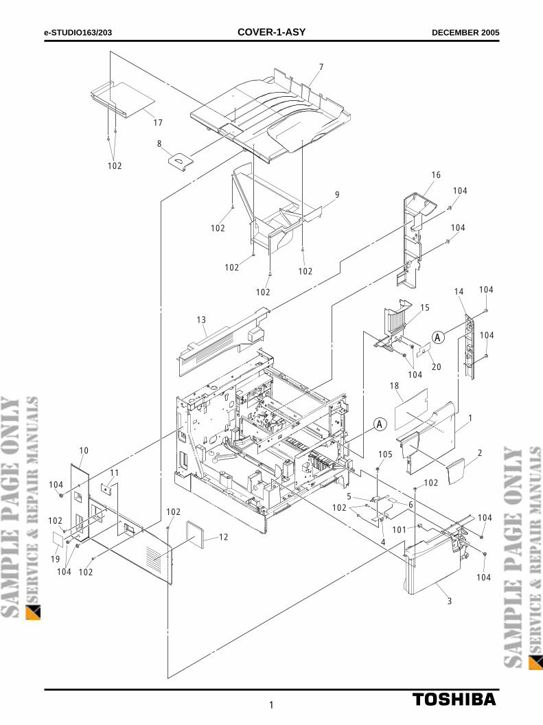
COVER-1-ASY ............................................ 1
COVER-2-ASY ............................................ 2
COVER-3-ASY ............................................ 3
CONTROL-PANEL-ASY .............................. 4
BASE-FRAME-ASY..................................... 5
FRONT-FRAME-ASY .................................. 6
REAR-FRAME-ASY .................................... 7
STAY-ASY ................................................... 8
OPTICAL-FRAME-ASY ............................... 9
OPTICAL-DRIVE-ASY .............................. 10
COVER-GUIDE-ASY................................. 11
MAIN-DRIVE-ASY ..................................... 12
BYPASS-ASY ............................................ 13
BYPASS-FEEDER-ASY ............................ 14
GUIDE-ALIGNING-ASY ............................ 15
ALIGNING-ASY ......................................... 16
PLATEN-ASY ............................................ 17
MAIN-CHARGER-ASY .............................. 18
TRANSPORT-CHARGER-ASY ................. 19
CLEANER-ASY ......................................... 20
DEVELOPER-ASY .................................... 21
RECYCLE-ASY ......................................... 22
FUSER-1-ASY........................................... 23
FUSER-2-ASY........................................... 24
DRAWER-ASY .......................................... 25
JIGS & GREASE ..................................... 101
DOWNLOAD JIGS .................................. 102
SUPPLIES ............................................... 103
REPLACE UNIT ...................................... 104
PM-KIT .................................................... 105
1
e-STUDIO163/203 DECEMBER 2005
8
7
102
102
102
102
102
102
101
102
105
102
104
104
104104
19
102
104
104
104
104
104
102
17
16
14
15
20
13
10
11
12
1
2
3
6 5
4
9
18
A
A
COVER-1-ASY
PC BOARD REPAIR MANUALMULTIFUNCTIONAL DIGITAL SYSTEMS
e-STUDIO163/165/203/205e-STUDIO166/167/206/207/237
File No. RME050003A0R05092196500-TTECVer01_2007-03
© June 2006 TOSHIBA TEC CORPORATION All rights reserved e-STUDIO163/165/166/167/203/205/206/207/237CONTENTS
1
CONTENTS
1. SYSTEM BLOCK DIAGRAM ........................................................................................ 1-11.1 e-STUDIO163/166/203/206................................................................................................. 1-11.2 e-STUDIO165/205............................................................................................................... 1-21.3 e-STUDIO167/207/237........................................................................................................ 1-3
2. GENERAL DESCRIPTION OF MAIN IC....................................................................... 2-12.1 ASIC (EC/N106) .................................................................................................................. 2-1
2.1.1 Functions.................................................................................................................. 2-12.1.2 Pin assignment......................................................................................................... 2-12.1.3 Signals...................................................................................................................... 2-2
3. ELECTRIC CIRCUIT DIAGRAMS................................................................................. 3-13.1 Main circuit (MAIN board: e-STUDIO163/165/203/205) ...................................................... 3-23.2 SRAM circuit (SRAM board: e-STUDIO163/165/203/205) ................................................ 3-363.3 Laser drive circuit (LDR board).......................................................................................... 3-373.4 H-sync signal detection circuit (SNS board) ...................................................................... 3-393.5 Fuse circuit (FUS board).................................................................................................... 3-403.6 Control panel circuit (LPNL board: e-STUDIO163/166/203/206)....................................... 3-413.7 Control panel circuit (HPNL board: e-STUDIO165/205) .................................................... 3-453.8 Paper feed control circuit (PFC board: GH-1050).............................................................. 3-493.9 Facsimile circuit (FAX board: GD-1220) ............................................................................ 3-533.10 Telephone line network control circuit (NCU board: GD-1220NA/TW).............................. 3-583.11 Telephone line network control circuit (NCU board: GD-1220EU/AU) .............................. 3-603.12 TELBOOK circuit (TELBOOK board: GJ-1040) ................................................................. 3-623.13 External keyboard circuit (OTK board: GJ-1040)............................................................... 3-633.14 Memory circuit (MEM board: GC-1240)............................................................................. 3-643.15 Main circuit (MAIN board: e-STUDIO166/206) .................................................................. 3-653.16 Main circuit (MAIN board: e-STUDIO167/207/237) ........................................................... 3-993.17 SRAM circuit (SRAM board: e-STUDIO166/167/206/207/237) ....................................... 3-1343.18 Control panel circuit (HPNL board: e-STUDIO167/207/237) ........................................... 3-1353.19 Paper feed control circuit (PFC board: GH-1060)............................................................ 3-139
07/03